EP2284995A1 - A linear transconductance cell with wide tuning range - Google Patents
A linear transconductance cell with wide tuning range Download PDFInfo
- Publication number
- EP2284995A1 EP2284995A1 EP10180436A EP10180436A EP2284995A1 EP 2284995 A1 EP2284995 A1 EP 2284995A1 EP 10180436 A EP10180436 A EP 10180436A EP 10180436 A EP10180436 A EP 10180436A EP 2284995 A1 EP2284995 A1 EP 2284995A1
- Authority
- EP
- European Patent Office
- Prior art keywords
- field effect
- effect transistors
- voltage
- series
- cell
- Prior art date
- Legal status (The legal status is an assumption and is not a legal conclusion. Google has not performed a legal analysis and makes no representation as to the accuracy of the status listed.)
- Withdrawn
Links
Images


Classifications
-
- H—ELECTRICITY
- H03—ELECTRONIC CIRCUITRY
- H03F—AMPLIFIERS
- H03F3/00—Amplifiers with only discharge tubes or only semiconductor devices as amplifying elements
- H03F3/45—Differential amplifiers
- H03F3/45071—Differential amplifiers with semiconductor devices only
- H03F3/45076—Differential amplifiers with semiconductor devices only characterised by the way of implementation of the active amplifying circuit in the differential amplifier
- H03F3/4508—Differential amplifiers with semiconductor devices only characterised by the way of implementation of the active amplifying circuit in the differential amplifier using bipolar transistors as the active amplifying circuit
- H03F3/45085—Long tailed pairs
-
- H—ELECTRICITY
- H03—ELECTRONIC CIRCUITRY
- H03F—AMPLIFIERS
- H03F1/00—Details of amplifiers with only discharge tubes, only semiconductor devices or only unspecified devices as amplifying elements
- H03F1/32—Modifications of amplifiers to reduce non-linear distortion
- H03F1/3211—Modifications of amplifiers to reduce non-linear distortion in differential amplifiers
-
- H—ELECTRICITY
- H03—ELECTRONIC CIRCUITRY
- H03F—AMPLIFIERS
- H03F3/00—Amplifiers with only discharge tubes or only semiconductor devices as amplifying elements
- H03F3/45—Differential amplifiers
- H03F3/45071—Differential amplifiers with semiconductor devices only
- H03F3/45076—Differential amplifiers with semiconductor devices only characterised by the way of implementation of the active amplifying circuit in the differential amplifier
- H03F3/45179—Differential amplifiers with semiconductor devices only characterised by the way of implementation of the active amplifying circuit in the differential amplifier using MOSFET transistors as the active amplifying circuit
-
- H—ELECTRICITY
- H03—ELECTRONIC CIRCUITRY
- H03F—AMPLIFIERS
- H03F2203/00—Indexing scheme relating to amplifiers with only discharge tubes or only semiconductor devices as amplifying elements covered by H03F3/00
- H03F2203/45—Indexing scheme relating to differential amplifiers
- H03F2203/45352—Indexing scheme relating to differential amplifiers the AAC comprising a combination of a plurality of transistors, e.g. Darlington coupled transistors
-
- H—ELECTRICITY
- H03—ELECTRONIC CIRCUITRY
- H03F—AMPLIFIERS
- H03F2203/00—Indexing scheme relating to amplifiers with only discharge tubes or only semiconductor devices as amplifying elements covered by H03F3/00
- H03F2203/45—Indexing scheme relating to differential amplifiers
- H03F2203/45384—Indexing scheme relating to differential amplifiers the AAC comprising common gate stages in the source circuit of the AAC before the common source coupling in which the common gate stage being controlled
-
- H—ELECTRICITY
- H03—ELECTRONIC CIRCUITRY
- H03F—AMPLIFIERS
- H03F2203/00—Indexing scheme relating to amplifiers with only discharge tubes or only semiconductor devices as amplifying elements covered by H03F3/00
- H03F2203/45—Indexing scheme relating to differential amplifiers
- H03F2203/45392—Indexing scheme relating to differential amplifiers the AAC comprising resistors in the source circuit of the AAC before the common source coupling
Definitions
- the present disclosure relates generally to electronics, and more specifically, to a transconductance cell with good tuning range.
- Filters are used extensively today in almost every electronic application.
- a filter is an electrical network that alters the amplitude and/or phase characteristics of a signal with respect to frequency.
- a filter may be used in an electronic circuit to emphasize signals in certain frequency ranges and reject signals in other frequency ranges.
- the behavior of a filter may be described mathematically in the frequency-domain in terms of its transfer function.
- the transfer function describes the effect of the filter on the amplitude of the input signal at various frequencies.
- a transconductance cell is often used as a basic building block in filter design, such as low-pass filters.
- a low-pass filter passes low frequency signals, and rejects signals at frequencies above the filter's pole frequency.
- the filter's pole frequency is equal to the frequency at which the signal output drops 3 dB below the center frequency.
- the range of frequencies below the pole frequency is known as the filter's passband.
- An ideal low-pass filter has a transfer function with a flat response over its passband.
- the low-pass filter may experience signal distortions in its passband due to the nonlinearity of the Gm-cell. Accordingly, there is a continuing need in the art for Gm-cells with improved linearity for low-pass filter design.
- a transconductance cell includes a tunable degeneration circuit having a plurality of field effect transistors connected in series, each of the field effect transistors having a gate configured to receive a tuning voltage.
- a transconductance cell in another aspect of the present invention, includes a tunable degeneration circuit having a tapped voltage divider network configured to receive a tuning voltage.
- the tunable degeneration circuit also includes a plurality of field effect transistors connected in series, each of the field effect transistors having a gate coupled to a different one of the taps.
- a differential transconductance cell in yet another aspect of the present invention, includes a pair of input transistors, and a tunable degeneration circuit having a first leg comprising a plurality of field effect transistors connected in series and a second leg comprising a plurality of field effect transistors connected in series, one end of the first leg being coupled to a first one of the input transistors and one end of the second leg being coupled to a second one of the input transistors, each of the field effect transistors having a gate configured to receive a tuning voltage.
- a differential transconductance cell in still another aspect of the present invention, includes a pair of input devices, and a tunable degeneration circuit having a first leg comprising a plurality of field effect transistors connected in series and a second leg comprising a plurality of field effect transistors connected in series, one end of the first leg being coupled to a first one of the input transistors and one end of the second leg being coupled to a second one of the input transistors.
- the tunable degeneration circuit further includes a tapped voltage divider network configured to receive a tuning voltage with each pair of field effect transistors having gates coupled to a different one of a plurality of the taps, each of the field effect transistor pairs comprising one of the field effect transistors from the first leg and one of the field effect transistors from the second leg.
- a filter in a further aspect of the present invention, includes a transconductance cell having a tunable degeneration circuit, the tunable degeneration circuit having a plurality of field effect transistors connected in series, each of the field effect transistors having a gate configured to receive a tuning voltage.
- the filter also includes a shunt capacitor coupled to the output of the transconductance cell.
- FIG. 1 is a functional block diagram of a filter using a Gm-cell
- FIG. 2 is a schematic diagram of a Gm-cell employing a symmetrical source-coupled differential amplifier
- FIG. 3 is a schematic diagram of a tunable Gm-cell employing field effect transistors (FETs) as variable resistors in a degeneration circuit;
- FETs field effect transistors
- FIG. 4 is a schematic diagram of a tunable Gm-cell employing field effect transistors (FETs) in combination with fixed resistors in the degeneration circuit;
- FETs field effect transistors
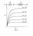
- FIG. 5 is a graphical illustration showing the drain characteristic curves of a FET.
- FIG. 6 is a schematic diagram of a tunable Gm-cell employing degeneration FETs operating in the linear portion of the triode region.
- FIG. 1 is a functional block diagram of a filter.
- the filter 102 may employ a Gm-cell 104, with a shunt capacitor C in the output circuit, to generate the desired filter response.
- the filter's pole frequency is equal to the frequency at which the signal output V out drops 3 dB below the center frequency.
- FIG. 2 is a schematic diagram of a Gm-cell comprising a symmetrical source-coupled differential amplifier.
- the Gm-cell 104 is shown with a pair of input n-channel field effect transistors (FET) 202a and 202b, but could alternatively be implemented with a pair of p-channel FETs.
- Each input FET 202a and 202b includes an active load 204a and 204b, respectively, in its drain circuit.
- the active loads are shown as p-channel FETs, but could alternatively be n-channel FETs.
- the Gm-cell 104 may also include a degeneration circuit 206 implemented with a feedback resistor R in the source circuit of each input FET 202a and 202b.
- a constant current source 208 may be coupled to the degeneration circuit 206.
- the feedback resistors R may be used to improve the linearity of the Gm-cell 104, resulting in a transfer function with a relatively flat response over its passband.
- the feedback resistors R result in a Gm-cell 104 with a fixed transconductance, and therefore, it may be difficult to adjust the filter's passband to compensate for process, voltage and temperature variations.
- the transconductance of the Gm-cell should be tunable. This may be accomplished by replacing the fixed feedback resistor R with a variable one.
- FIG. 3 is a schematic diagram of a tunable Gm-cell which uses field effect transistors (FET) as variable feedback resistors in the degeneration circuit.
- the Gm-cell 104 may include a pair of input bipolar transistors 302a and 302b, each having an active load 304a and 304b, respectively, in its collector circuit.
- the Gm-cell 104 may also include a tunable degeneration circuit 306 implemented with a FET 308a and 308b in the emitter circuit of each input transistor 302a and 302b.
- a constant source 310 may be coupled to the tunable degeneration circuit 306.
- the FETs 308a and 308b provide a means for varying the transconductance of the Gm-cell 104 by applying a tuning voltage to the gates.
- the drawback of this approach is that the linearity of the filter may suffer due to the nonlinearity of the FETs 308a and 308b.
- a pair of fixed resistors R may be used in the tunable degeneration circuit 306 with one inserted in the emitter circuit of each input transistor 302a and 302b as shown in FIG. 4 .
- a degeneration circuit implemented with fixed resistors in combination with FETs as shown in FIG. 4 may result in some improvement in linearity while reducing the tuning range.
- Each drain characteristic curve plots the drain-to-source current (I DS ) as a function of the drain-to-source voltage (V DS ) for a given gate-to-source voltage (V GS ).
- the drain characteristic curves may be divided into two regions: a triode region 502 and a saturation region 504.
- the resistance r DS of the FET is equal to the drain-to-source voltage divided by the drain-to-source current (V DS /I DS ), and can be derived from equation (2) as follows: r ds ⁇ 1 ⁇ Co ⁇ W L ⁇ V GS - V T - V DS 2
- Equation (3) may be rewritten as follows: r ds ⁇ 1 ⁇ Co ⁇ W L ⁇ V GS - V T ⁇ 1 - V DS 2 ⁇ V GS - V T
- the resistance r DS of the FET is independent of the drain-to-source voltage V DS when the last term in the denominator becomes zero.
- Equation (5) shows that the linearity of the FET may be increased by decreasing the quiescent drain-to-source voltage V DS and increasing the tuning or gate-to-source voltage V GS . This is consistent with FIG. 5 which shows that each drain characteristic curve is more linear at lower drain-to-source voltages V DS . FIG. 5 also shows that for any given drain-to-source voltage V DS in the triode region 502, the drain characteristic curves become progressively more linear as the gate-to-source voltage V GS is increased.
- FIG. 6 is a schematic diagram of a tunable Gm-cell which uses degeneration FETs operating in the linear portion of the triode region. This approach results in a wide tuning range without compromising the linearity of the cell.
- the Gm-cell 104 may include a pair of input devices. These input devices are shown in FIG. 6 as bipolar transistors 602a and 602b, but alternatively, may be any input device. In this example, the bipolar transistors 602a and 602b may each have an active load 604a and 604b in their respective collector circuits.
- the Gm-cell 104 may also include a tunable degeneration circuit 606 coupled to the input devices, and in the example shown in FIG. 6 , coupled to the emitters of the bipolar transistors 602a and 602b.
- a constant source 608 may be coupled to the tunable degeneration circuit 606.
- the tunable degeneration circuit 606 may include a first leg 610a coupled to the emitter of one bipolar transistor 602a and a second leg 610b coupled to the emitter of the other bipolar transistor 602b.
- the first leg 610a may include a feedback resistor R connected in series with a first set of FETs (Q 11 - Q 1n ), and the second leg 610b may also include a feedback resistor R connected in series with a second set of FETs (Q 21 - Q 2n ).
- a "series" connection means that the same currents flow through the components.
- the feedback resistor and FETs in the first (or second leg) of the tunable generation circuit 606 are said to be in series because the same drain-to-source current I DS flows through each of them-
- the series "connection" can either be direct as shown or, where appropriate in the context, can be indirect, e.g., through intervening or intermediary devices or other means.
- the tunable degeneration circuit 606 may also include a tapped voltage divider network 612.
- the tapped voltage divider network 612 is shown with a number of resistors R b connected in series, although other voltage divider networks may be used.
- the tapped voltage divider network 612 includes a positive input for receiving a tuning voltage and a negative input connected to ground through a resistor R gnd .
- the tapped voltage divider network also includes n taps.
- the first tap T 1 is connected to the gates of the FETs Q 11 and Q 21 in the first and second legs 610a and 610b, respectively.
- the second tap T 2 is shown connected to the gates of the FETs Q 12 and Q 22
- in the n th tap T n is shown connected to the gates of the FETs Q 1n and Q 2n .
- the component values may be selected to yield a linear Gm-cell with good tuning range. This may be achieved in a variety of ways.
- a good starting point for selecting component values is the zero-excitation operating point of the bipolar transistors 602a and 602b.
- the zero-excitation operating point typically referred to as the "quiescent" point, may be selected to bias the transistors in the active region, and preferably, in the center of each transistor's output characteristic curve. With the transistors operating at their respective quiescent points, time-varying excursions of the input signal below the pole frequency should be faithfully reproduced at the output.
- the drain-to-source voltage V DS for each FET in the degeneration circuit 606 may be computed using equation (2).
- the Gm-cell may operate with reasonable linearity with a single FET in each leg 610a and 610b of the degeneration circuit 606 if the computed drain-to-source voltage V DS is relatively small. However, as the computed drain-to-source voltage V DS increases, a single FET may begin to operate in a non-linear manner as seen by inspection from the drain characteristic curves of FIG. 5 .
- the drain-to-source voltage V DS of each FET can be reduced. Referring to FIG. 5 , this moves the operating point of each FET down the drain characteristic curve towards the linear portion of the triode region resulting in a more linear Gm-cell.
- V GS gate-to-source voltage
- the gate-to-source voltage V GS for the lower FETs Q 11 and Q 21 may be set by the resistor R gnd , at the negative input to the voltage divider network 612.
- the gate-to-source voltages V GS applied to the FETs may be progressively increased from the bottom of the voltage divider network to the top with a series of resistors R b between each tap.
- the gate-to-source voltage V GS applied to each FET should be increased to compensate for the drain-to-source V DS voltage drop of the FET immediately below it.
- the gate-to-source V GS of the FETs Q 12 and Q 22 should be V GS1 + ⁇ V
- the gate-to-source V GS of the FETs Q 1n and Q 2n should be V GS1 + n ⁇ V, where ⁇ V can be represented by the following equation: ⁇ ⁇ V ⁇ I DC 2 . r ds
- a transconductance cell comprising: a tunable degeneration circuit having a plurality of field effect transistors connected in series, each of the field effect transistors having a gate configured to receive a tuning voltage.
- the tunable degeneration circuit further may comprise a feedback resistor connected in series with the field effect transistors.
- the tunable degeneration circuit may further comprise a tapped voltage divider network configured to apply the tuning voltage to each of the field effect transistors through a different one of the taps.
- the tapped voltage divider network may be configured to generate a differential voltage between each adjacent pair of the taps when the tuning voltage is applied to the tapped voltage divider network, the differential voltage being equal to the quiescent drain-to-source voltage of one of the field effect transistors.
- the tapped voltage divider network may comprise one or more resistors connected in series, each of said one or more resistors being positioned between a different adjacent pair of the taps.
- Each of said one or more resistors may have a value that results in a differential voltage between each adjacent pair of the taps when the tuning voltage is applied to the tapped voltage divider network, the differential voltage being equal to the quiescent drain-to-source voltage of one of the field effect transistors.
- a transconductance cell comprising: a tunable degeneration circuit having a tapped voltage divider network configured to receive a tuning voltage, and a plurality of field effect transistors connected in series, each of the field effect transistors having a gate coupled to a different one of the taps.
- the tunable degeneration circuit may further comprise a feedback resistor connected in series with the field effect transistors.
- the tapped voltage divider network may comprise one or more resistors connected in series, each of said one or more resistors being positioned between a different adjacent pair of the taps.
- Each of said one or more resistors may have a value that results in a differential voltage between each different adjacent pair of the taps when the tuning voltage is applied to the tapped voltage divider network, the differential voltage being equal to the quiescent drain-to-source voltage of one of the field effect transistors.
- a differential transconductance cell comprising: a pair of input transistors; and a tunable degeneration circuit having a first leg comprising a plurality of field effect transistors connected in series and a second leg comprising a plurality of field effect transistors connected in series, one end of the first leg being coupled to a first one of the input transistors and one end of the second leg being coupled to a second one of the input transistors, each of the field effect transistors having a gate configured to receive a tuning voltage.
- the tunable degeneration circuit may further comprise a first feedback resistor connected in series with the field effect transistors in the first leg and a second feedback resistor connected in series with the field effect transistors in the second leg.
- the tunable degeneration circuit may further comprise a tapped voltage divider network, each of a plurality of the taps being configured to apply the tuning voltage to a different pair of the field effect transistors, each of field effect transistor pairs comprising one of the field effect transistors from the first leg and one of the field effect transistors from the second leg.
- the tapped voltage divider network may be configured to generate a differential voltage between each of adjacent pair of the taps when the tuning voltage is applied to the tapped voltage divider network, the differential voltage being equal to the quiescent drain-to-source voltage of one of the field effect transistors.
- the tapped voltage divider network may comprise one or more resistors connected in series, each of said one or more resistors being positioned between a different adjacent pair of the taps.
- Each of said one or more resistors may have a value that results in a differential voltage between each of the different adjacent pairs of the taps when the tuning voltage is applied to the tapped voltage divider network, the differential voltage being equal to the quiescent drain-to-source voltage of one of the field effect transistors.
- a differential transconductance cell comprising: a pair of input devices; and a tunable degeneration circuit having a first leg comprising a plurality of field effect transistors connected in series and a second leg comprising a plurality of field effect transistors connected in series, one end of the first leg being coupled to a first one of the input transistors and one end of the second leg being coupled to a second one of the input transistors, the tunable degeneration circuit further having a tapped voltage divider network configured to receive a tuning voltage, each pair of field effect transistors having gates coupled to a different one of a plurality of the taps, each of the field effect transistor pairs comprising one of the field effect transistors from the first leg and one of the field effect transistors from the second leg.
- the tunable degeneration circuit may further comprise a first feedback resistor connected in series with the field effect transistors in the first leg, and a second feedback resistor connected in series with the field effect transistors in the second leg.
- the tapped voltage divider network may further comprise one or more resistors connected in series, each of said one or more resistors being positioned between a different adjacent pair of the taps.
- Each of said one or more resistors may have a value that results in a differential voltage between each of the different adjacent pairs of the taps when the tuning voltage is applied to the tapped voltage divider network, the differential voltage being equal to the quiescent drain-to-source voltage of the field effect transistors.
- a filter comprising: a transconductance cell having a tunable degeneration circuit, the tunable degeneration circuit having a plurality of field effect transistors connected in series, each of the field effect transistors having a gate configured to receive a tuning voltage; and a shunt capacitor coupled to the output of the transconductance cell.
Abstract
Description
- The present disclosure relates generally to electronics, and more specifically, to a transconductance cell with good tuning range.
- Filters are used extensively today in almost every electronic application. A filter is an electrical network that alters the amplitude and/or phase characteristics of a signal with respect to frequency. Thus, a filter may be used in an electronic circuit to emphasize signals in certain frequency ranges and reject signals in other frequency ranges. The behavior of a filter may be described mathematically in the frequency-domain in terms of its transfer function. The transfer function describes the effect of the filter on the amplitude of the input signal at various frequencies.
- A transconductance cell (Gm-cell) is often used as a basic building block in filter design, such as low-pass filters. A low-pass filter passes low frequency signals, and rejects signals at frequencies above the filter's pole frequency. The filter's pole frequency is equal to the frequency at which the signal output drops 3 dB below the center frequency. The range of frequencies below the pole frequency is known as the filter's passband. An ideal low-pass filter has a transfer function with a flat response over its passband. However, in actual implementation, the low-pass filter may experience signal distortions in its passband due to the nonlinearity of the Gm-cell. Accordingly, there is a continuing need in the art for Gm-cells with improved linearity for low-pass filter design.
- In one aspect of the present invention, a transconductance cell includes a tunable degeneration circuit having a plurality of field effect transistors connected in series, each of the field effect transistors having a gate configured to receive a tuning voltage.
- In another aspect of the present invention, a transconductance cell includes a tunable degeneration circuit having a tapped voltage divider network configured to receive a tuning voltage. The tunable degeneration circuit also includes a plurality of field effect transistors connected in series, each of the field effect transistors having a gate coupled to a different one of the taps.
- In yet another aspect of the present invention, a differential transconductance cell includes a pair of input transistors, and a tunable degeneration circuit having a first leg comprising a plurality of field effect transistors connected in series and a second leg comprising a plurality of field effect transistors connected in series, one end of the first leg being coupled to a first one of the input transistors and one end of the second leg being coupled to a second one of the input transistors, each of the field effect transistors having a gate configured to receive a tuning voltage.
- In still another aspect of the present invention, a differential transconductance cell includes a pair of input devices, and a tunable degeneration circuit having a first leg comprising a plurality of field effect transistors connected in series and a second leg comprising a plurality of field effect transistors connected in series, one end of the first leg being coupled to a first one of the input transistors and one end of the second leg being coupled to a second one of the input transistors. The tunable degeneration circuit further includes a tapped voltage divider network configured to receive a tuning voltage with each pair of field effect transistors having gates coupled to a different one of a plurality of the taps, each of the field effect transistor pairs comprising one of the field effect transistors from the first leg and one of the field effect transistors from the second leg.
- In a further aspect of the present invention, a filter includes a transconductance cell having a tunable degeneration circuit, the tunable degeneration circuit having a plurality of field effect transistors connected in series, each of the field effect transistors having a gate configured to receive a tuning voltage. The filter also includes a shunt capacitor coupled to the output of the transconductance cell.
- It is understood that other embodiments of the present invention will become readily apparent to those skilled in the art from the following detailed description, wherein various embodiments of the invention are shown and described by way of illustration. As will be realized, the invention is capable of other and different embodiments and its several details are capable of modification in various other respects, all without departing from the spirit and scope of the present invention. Accordingly, the drawings and detailed description are to be regarded as illustrative in nature and not as restrictive.
- Aspects of the present invention are illustrated by way of example, and not by way of limitation, in the accompanying drawings wherein:
-
FIG. 1 is a functional block diagram of a filter using a Gm-cell; -
FIG. 2 is a schematic diagram of a Gm-cell employing a symmetrical source-coupled differential amplifier; -
FIG. 3 is a schematic diagram of a tunable Gm-cell employing field effect transistors (FETs) as variable resistors in a degeneration circuit; -
FIG. 4 is a schematic diagram of a tunable Gm-cell employing field effect transistors (FETs) in combination with fixed resistors in the degeneration circuit; -
FIG. 5 is a graphical illustration showing the drain characteristic curves of a FET; and -
FIG. 6 is a schematic diagram of a tunable Gm-cell employing degeneration FETs operating in the linear portion of the triode region. - The detailed description set forth below in connection with the appended drawings is intended as a description of various embodiments of the present invention and is not intended to represent the only embodiments in which the present invention may be practiced. Each embodiment described in this disclosure is provided merely as an example or illustration of the present invention, and should not necessarily be construed as preferred or advantageous over other embodiments. The detailed description includes specific details for the purpose of providing a thorough understanding of the present invention. However, it will be apparent to those skilled in the art that the present invention may be practiced without these specific details. In some instances, well-known structures and devices are shown in block diagram form in order to avoid obscuring the concepts of the present invention.
-
FIG. 1 is a functional block diagram of a filter. Thefilter 102 may employ a Gm-cell 104, with a shunt capacitor C in the output circuit, to generate the desired filter response. The transfer function of thefilter 102 may be represented in the frequency domain by the following equation:
where Gm is the transconductance of the Gm-cell. - As explained earlier, the filter's pole frequency is equal to the frequency at which the signal output Vout drops 3 dB below the center frequency. With this definition in mind, one can readily see by inspection that the pole frequency varies with transconductance, and therefore, the bandpass of the filter may be controlled by adjusting the transconductance of the Gm-
cell 104. -
FIG. 2 is a schematic diagram of a Gm-cell comprising a symmetrical source-coupled differential amplifier. The Gm-cell 104 is shown with a pair of input n-channel field effect transistors (FET) 202a and 202b, but could alternatively be implemented with a pair of p-channel FETs. Each input FET 202a and 202b includes an active load 204a and 204b, respectively, in its drain circuit. The active loads are shown as p-channel FETs, but could alternatively be n-channel FETs. The Gm-cell 104 may also include adegeneration circuit 206 implemented with a feedback resistor R in the source circuit of each input FET 202a and 202b. A constantcurrent source 208 may be coupled to thedegeneration circuit 206. - The feedback resistors R may be used to improve the linearity of the Gm-
cell 104, resulting in a transfer function with a relatively flat response over its passband. Unfortunately, the feedback resistors R result in a Gm-cell 104 with a fixed transconductance, and therefore, it may be difficult to adjust the filter's passband to compensate for process, voltage and temperature variations. To ensure the passband of the filter remains constant across process, voltage and temperature variations, the transconductance of the Gm-cell should be tunable. This may be accomplished by replacing the fixed feedback resistor R with a variable one. -
FIG. 3 is a schematic diagram of a tunable Gm-cell which uses field effect transistors (FET) as variable feedback resistors in the degeneration circuit. The Gm-cell 104 may include a pair of input bipolar transistors 302a and 302b, each having an active load 304a and 304b, respectively, in its collector circuit. The Gm-cell 104 may also include atunable degeneration circuit 306 implemented with a FET 308a and 308b in the emitter circuit of each input transistor 302a and 302b. Aconstant source 310 may be coupled to thetunable degeneration circuit 306. - The FETs 308a and 308b provide a means for varying the transconductance of the Gm-
cell 104 by applying a tuning voltage to the gates. The drawback of this approach is that the linearity of the filter may suffer due to the nonlinearity of the FETs 308a and 308b. To improve this situation, a pair of fixed resistors R may be used in thetunable degeneration circuit 306 with one inserted in the emitter circuit of each input transistor 302a and 302b as shown inFIG. 4 . A degeneration circuit implemented with fixed resistors in combination with FETs as shown inFIG. 4 may result in some improvement in linearity while reducing the tuning range. - The nonlinearity of the FET will be discussed with reference to the set of drain characteristic curves shown in
FIG. 5 . Each drain characteristic curve plots the drain-to-source current (IDS) as a function of the drain-to-source voltage (VDS) for a given gate-to-source voltage (VGS). - The drain characteristic curves may be divided into two regions: a
triode region 502 and a saturation region 504. In thetriode region 502, the drain characteristics are given by:
where: - µ is the mobility of the majority carrier;
- Co is the gate capacitance per unit area;
- L is the channel length;
- W is the channel width; and
- VT is the threshold gate-to-source voltage VGS for the FET to begin conducting.
- The resistance rDS of the FET is equal to the drain-to-source voltage divided by the drain-to-source current (VDS/IDS), and can be derived from equation (2) as follows:

- Equation (3) may be rewritten as follows:

- One can readily see by inspection from equation (4) that the resistance rDS of the FET is independent of the drain-to-source voltage VDS when the last term in the denominator becomes zero. In other words, once the gate-to-source voltage VGS is tuned to a fixed value to compensate for process, voltage and temperature variations, the feedback resistance rDS is constant when the last term in the denominator becomes zero, regardless of changes in the drain-to-source voltage VDS when a signal is applied to the base of the input transistors 302a and 302b (see
FIG. 3 ). Accordingly, this term may provide a good indication of the linearity of the FET, and is represented below as a linearity factor fLIN :
- Equation (5) shows that the linearity of the FET may be increased by decreasing the quiescent drain-to-source voltage VDS and increasing the tuning or gate-to-source voltage VGS. This is consistent with
FIG. 5 which shows that each drain characteristic curve is more linear at lower drain-to-source voltages VDS.FIG. 5 also shows that for any given drain-to-source voltage VDS in thetriode region 502, the drain characteristic curves become progressively more linear as the gate-to-source voltage VGS is increased. -
FIG. 6 is a schematic diagram of a tunable Gm-cell which uses degeneration FETs operating in the linear portion of the triode region. This approach results in a wide tuning range without compromising the linearity of the cell. The Gm-cell 104 may include a pair of input devices. These input devices are shown inFIG. 6 as bipolar transistors 602a and 602b, but alternatively, may be any input device. In this example, the bipolar transistors 602a and 602b may each have an active load 604a and 604b in their respective collector circuits. The Gm-cell 104 may also include atunable degeneration circuit 606 coupled to the input devices, and in the example shown inFIG. 6 , coupled to the emitters of the bipolar transistors 602a and 602b. Aconstant source 608 may be coupled to thetunable degeneration circuit 606. - As shown in
FIG. 6 , thetunable degeneration circuit 606 may include a first leg 610a coupled to the emitter of one bipolar transistor 602a and a second leg 610b coupled to the emitter of the other bipolar transistor 602b. The first leg 610a may include a feedback resistor R connected in series with a first set of FETs (Q11 - Q1n), and the second leg 610b may also include a feedback resistor R connected in series with a second set of FETs (Q21 - Q2n). A "series" connection means that the same currents flow through the components. InFIG. 6 , the feedback resistor and FETs in the first (or second leg) of thetunable generation circuit 606 are said to be in series because the same drain-to-source current IDS flows through each of them- The series "connection" can either be direct as shown or, where appropriate in the context, can be indirect, e.g., through intervening or intermediary devices or other means. - The
tunable degeneration circuit 606 may also include a tappedvoltage divider network 612. In the example shown inFIG. 6 , the tappedvoltage divider network 612 is shown with a number of resistors Rb connected in series, although other voltage divider networks may be used. The tappedvoltage divider network 612 includes a positive input for receiving a tuning voltage and a negative input connected to ground through a resistor Rgnd. The tapped voltage divider network also includes n taps. As shown inFIG. 6 , the first tap T1 is connected to the gates of the FETs Q11 and Q21 in the first and second legs 610a and 610b, respectively. Similarly, the second tap T2 is shown connected to the gates of the FETs Q12 and Q22, and in the n th tap Tn is shown connected to the gates of the FETs Q1n and Q2n. - The component values may be selected to yield a linear Gm-cell with good tuning range. This may be achieved in a variety of ways. A good starting point for selecting component values is the zero-excitation operating point of the bipolar transistors 602a and 602b. The zero-excitation operating point, typically referred to as the "quiescent" point, may be selected to bias the transistors in the active region, and preferably, in the center of each transistor's output characteristic curve. With the transistors operating at their respective quiescent points, time-varying excursions of the input signal below the pole frequency should be faithfully reproduced at the output.
- Once the quiescent current through each bipolar transistor 602a and 602b is determined, the drain-to-source voltage VDS for each FET in the
degeneration circuit 606 may be computed using equation (2). The Gm-cell may operate with reasonable linearity with a single FET in each leg 610a and 610b of thedegeneration circuit 606 if the computed drain-to-source voltage VDS is relatively small. However, as the computed drain-to-source voltage VDS increases, a single FET may begin to operate in a non-linear manner as seen by inspection from the drain characteristic curves ofFIG. 5 . By using multiple FETs in each leg 610a and 610b of thedegeneration circuit 606, the drain-to-source voltage VDS of each FET can be reduced. Referring toFIG. 5 , this moves the operating point of each FET down the drain characteristic curve towards the linear portion of the triode region resulting in a more linear Gm-cell. - Once the appropriate number of FETs are determined, further improvements in linearity may be achieved by increasing the gate-to-source voltage VGS. This may be achieved with the
voltage divider network 612 in thedegeneration circuit 606. The gate-to-source voltage VGS for the lower FETs Q11 and Q21 (VGS1) may be set by the resistor Rgnd, at the negative input to thevoltage divider network 612. The gate-to-source voltages VGS applied to the FETs may be progressively increased from the bottom of the voltage divider network to the top with a series of resistors Rb between each tap. The gate-to-source voltage VGS applied to each FET should be increased to compensate for the drain-to-source VDS voltage drop of the FET immediately below it. Thus, the gate-to-source VGS of the FETs Q12 and Q22 should be VGS1 + ΔV, and the gate-to-source VGS of the FETs Q1n and Q2n should be VGS1 + nΔV, where ΔV can be represented by the following equation:
- The previous description of the disclosed embodiments is provided to enable any person skilled in the art to make or use the present invention. Various modifications to these embodiments will be readily apparent to those skilled in the art, and the generic principles defined herein may be applied to other embodiments without departing from the spirit or scope of the invention. Thus, the present invention is not intended to be limited to the embodiments shown herein but is to be accorded the widest scope consistent with the principles and novel features disclosed herein.
- According to an aspect of the present invention there is provided a transconductance cell, comprising: a tunable degeneration circuit having a plurality of field effect transistors connected in series, each of the field effect transistors having a gate configured to receive a tuning voltage.
- The tunable degeneration circuit further may comprise a feedback resistor connected in series with the field effect transistors.
- The tunable degeneration circuit may further comprise a tapped voltage divider network configured to apply the tuning voltage to each of the field effect transistors through a different one of the taps.
- The tapped voltage divider network may be configured to generate a differential voltage between each adjacent pair of the taps when the tuning voltage is applied to the tapped voltage divider network, the differential voltage being equal to the quiescent drain-to-source voltage of one of the field effect transistors.
- The tapped voltage divider network may comprise one or more resistors connected in series, each of said one or more resistors being positioned between a different adjacent pair of the taps.
- Each of said one or more resistors may have a value that results in a differential voltage between each adjacent pair of the taps when the tuning voltage is applied to the tapped voltage divider network, the differential voltage being equal to the quiescent drain-to-source voltage of one of the field effect transistors.
- According to an aspect of the present invention there is provided a transconductance cell, comprising: a tunable degeneration circuit having a tapped voltage divider network configured to receive a tuning voltage, and a plurality of field effect transistors connected in series, each of the field effect transistors having a gate coupled to a different one of the taps.
- The tunable degeneration circuit may further comprise a feedback resistor connected in series with the field effect transistors.
- The tapped voltage divider network may comprise one or more resistors connected in series, each of said one or more resistors being positioned between a different adjacent pair of the taps.
- Each of said one or more resistors may have a value that results in a differential voltage between each different adjacent pair of the taps when the tuning voltage is applied to the tapped voltage divider network, the differential voltage being equal to the quiescent drain-to-source voltage of one of the field effect transistors.
- According to an aspect of the present invention there is provided a differential transconductance cell, comprising: a pair of input transistors; and a tunable degeneration circuit having a first leg comprising a plurality of field effect transistors connected in series and a second leg comprising a plurality of field effect transistors connected in series, one end of the first leg being coupled to a first one of the input transistors and one end of the second leg being coupled to a second one of the input transistors, each of the field effect transistors having a gate configured to receive a tuning voltage.
- The tunable degeneration circuit may further comprise a first feedback resistor connected in series with the field effect transistors in the first leg and a second feedback resistor connected in series with the field effect transistors in the second leg.
- The tunable degeneration circuit may further comprise a tapped voltage divider network, each of a plurality of the taps being configured to apply the tuning voltage to a different pair of the field effect transistors, each of field effect transistor pairs comprising one of the field effect transistors from the first leg and one of the field effect transistors from the second leg.
- The tapped voltage divider network may be configured to generate a differential voltage between each of adjacent pair of the taps when the tuning voltage is applied to the tapped voltage divider network, the differential voltage being equal to the quiescent drain-to-source voltage of one of the field effect transistors.
- The tapped voltage divider network may comprise one or more resistors connected in series, each of said one or more resistors being positioned between a different adjacent pair of the taps.
- Each of said one or more resistors may have a value that results in a differential voltage between each of the different adjacent pairs of the taps when the tuning voltage is applied to the tapped voltage divider network, the differential voltage being equal to the quiescent drain-to-source voltage of one of the field effect transistors.
- According to an aspect of the present invention there is provided a differential transconductance cell, comprising: a pair of input devices; and a tunable degeneration circuit having a first leg comprising a plurality of field effect transistors connected in series and a second leg comprising a plurality of field effect transistors connected in series, one end of the first leg being coupled to a first one of the input transistors and one end of the second leg being coupled to a second one of the input transistors, the tunable degeneration circuit further having a tapped voltage divider network configured to receive a tuning voltage, each pair of field effect transistors having gates coupled to a different one of a plurality of the taps, each of the field effect transistor pairs comprising one of the field effect transistors from the first leg and one of the field effect transistors from the second leg.
- The tunable degeneration circuit may further comprise a first feedback resistor connected in series with the field effect transistors in the first leg, and a second feedback resistor connected in series with the field effect transistors in the second leg.
- The tapped voltage divider network may further comprise one or more resistors connected in series, each of said one or more resistors being positioned between a different adjacent pair of the taps.
- Each of said one or more resistors may have a value that results in a differential voltage between each of the different adjacent pairs of the taps when the tuning voltage is applied to the tapped voltage divider network, the differential voltage being equal to the quiescent drain-to-source voltage of the field effect transistors.
- According to an aspect of the present invention there is provided a filter, comprising: a transconductance cell having a tunable degeneration circuit, the tunable degeneration circuit having a plurality of field effect transistors connected in series, each of the field effect transistors having a gate configured to receive a tuning voltage; and a shunt capacitor coupled to the output of the transconductance cell.
Claims (3)
- A transconductance cell comprising;
a tunable degeneration circuit having a plurality of field effect transistors connected in series, each of the field effect transistors having a gate configured to receive a tuning voltage, wherein the tunable degeneration circuit further comprises a tapped voltage divider network configured to apply the tuning voltage to each of the field effect transistors through a different one of the taps, wherein each of said one or more resistors has a value that results in a differential voltage between each adjacent pair of the taps when the tuning voltage is applied to the tapped voltage divider network, the differential voltage being equal to the quiescent drain-to-source voltage of one of the field effect transistors. - The transconductance cell of claim 1 wherein
each of the field effect transistors has a gate coupled to a different one of the taps, wherein the tapped voltage divider network comprises one or more resistors connected in series, each of said one or more resistors being positioned between a different adjacent pair of the taps. - The transconductance cell of claim 2 wherein the tunable degeneration circuit further comprises a feedback resistor connected in series with the field effect transistors.
Applications Claiming Priority (2)
| Application Number | Priority Date | Filing Date | Title |
|---|---|---|---|
| US10/944,145 US7145395B2 (en) | 2004-09-16 | 2004-09-16 | Linear transconductance cell with wide tuning range |
| EP05796291A EP1790074B1 (en) | 2004-09-16 | 2005-09-16 | A linear transconductance cell with wide tuning range |
Related Parent Applications (1)
| Application Number | Title | Priority Date | Filing Date |
|---|---|---|---|
| EP05796291.2 Division | 2005-09-16 |
Publications (1)
| Publication Number | Publication Date |
|---|---|
| EP2284995A1 true EP2284995A1 (en) | 2011-02-16 |
Family
ID=35562980
Family Applications (3)
| Application Number | Title | Priority Date | Filing Date |
|---|---|---|---|
| EP05796291A Not-in-force EP1790074B1 (en) | 2004-09-16 | 2005-09-16 | A linear transconductance cell with wide tuning range |
| EP10180436A Withdrawn EP2284995A1 (en) | 2004-09-16 | 2005-09-16 | A linear transconductance cell with wide tuning range |
| EP10180434A Withdrawn EP2284994A1 (en) | 2004-09-16 | 2005-09-16 | A linear transconductance cell with wide tuning range |
Family Applications Before (1)
| Application Number | Title | Priority Date | Filing Date |
|---|---|---|---|
| EP05796291A Not-in-force EP1790074B1 (en) | 2004-09-16 | 2005-09-16 | A linear transconductance cell with wide tuning range |
Family Applications After (1)
| Application Number | Title | Priority Date | Filing Date |
|---|---|---|---|
| EP10180434A Withdrawn EP2284994A1 (en) | 2004-09-16 | 2005-09-16 | A linear transconductance cell with wide tuning range |
Country Status (8)
| Country | Link |
|---|---|
| US (1) | US7145395B2 (en) |
| EP (3) | EP1790074B1 (en) |
| JP (1) | JP2008514130A (en) |
| AT (1) | ATE485625T1 (en) |
| CA (2) | CA2663936A1 (en) |
| DE (1) | DE602005024284D1 (en) |
| RU (1) | RU2007114053A (en) |
| WO (1) | WO2006034174A2 (en) |
Families Citing this family (4)
| Publication number | Priority date | Publication date | Assignee | Title |
|---|---|---|---|---|
| EP1848109B1 (en) * | 2006-04-19 | 2011-08-24 | Infineon Technologies AG | Temperature compensation of small signal gain for an amplifier stage |
| IT1392043B1 (en) * | 2008-09-12 | 2012-02-09 | St Microelectronics Srl | CURRENT DETECTION CIRCUIT FOR PWM APPLICATIONS WITH PULSE WIDTH MODULATION AND ITS PROCESS |
| KR101731753B1 (en) * | 2011-11-14 | 2017-04-28 | 인텔 코포레이션 | Macro-transistor devices |
| WO2014015277A2 (en) * | 2012-07-19 | 2014-01-23 | The Trustees Of Columbia University In The City Of New York | Circuits and methods for performing harmonic rejection mixing |
Citations (3)
| Publication number | Priority date | Publication date | Assignee | Title |
|---|---|---|---|---|
| WO1996013896A2 (en) * | 1994-10-28 | 1996-05-09 | Philips Electronics N.V. | A gain controllable amplifier, a receiver comprising a gain-controllable amplifier, and a method of controlling signal amplitudes |
| US20020050861A1 (en) * | 2000-02-15 | 2002-05-02 | Nguyen Thinh Cat | Variable transconductance variable gain amplifier utilizing a degenerated differential pair |
| US20040178850A1 (en) * | 2001-11-29 | 2004-09-16 | Sanyo Electric Co., Ltd. | Variable gain differential amplifier and multiplication circuit |
Family Cites Families (14)
| Publication number | Priority date | Publication date | Assignee | Title |
|---|---|---|---|---|
| US3852679A (en) * | 1972-12-26 | 1974-12-03 | Rca Corp | Current mirror amplifiers |
| EP0587965B1 (en) | 1992-09-16 | 1999-08-04 | STMicroelectronics S.r.l. | Differential transconductance stage, dynamically controlled by the input signal's amplitude |
| DE69523281T2 (en) | 1995-02-10 | 2002-07-11 | Alcatel Sa | Linear tunable Gm-C integrator |
| US5612648A (en) * | 1995-03-14 | 1997-03-18 | Standard Microsystems Corporation | Transconductance-capacitance filter with extended control range |
| JPH1168477A (en) * | 1997-08-12 | 1999-03-09 | Nec Corp | Tunable cmos operation transconductance amplifier |
| JPH11168334A (en) | 1997-12-02 | 1999-06-22 | Hitachi Ltd | Variable resistor, gain control amplifier mixer circuit and reception circuit |
| US5978241A (en) * | 1999-01-28 | 1999-11-02 | Industrial Technology Research Institute | Wide-linear range tunable transconductor using MOS |
| US6150885A (en) * | 1999-06-24 | 2000-11-21 | Lucent Technologies Inc. | Transconductance amplifier with wideband noise filtering |
| US6703682B2 (en) * | 1999-12-22 | 2004-03-09 | Texas Advanced Optoelectronic Solutions, Inc. | High sheet MOS resistor method and apparatus |
| JP3584893B2 (en) * | 2001-03-14 | 2004-11-04 | ソニー株式会社 | Filter circuit |
| JP2003168937A (en) * | 2001-11-29 | 2003-06-13 | Sanyo Electric Co Ltd | Variable gain type differential amplifying circuit, and multiplying circuit |
| JP2003168938A (en) | 2001-11-29 | 2003-06-13 | Sanyo Electric Co Ltd | Variable gain type differential amplifying circuit, and multiplying circuit |
| US6600373B1 (en) * | 2002-07-31 | 2003-07-29 | Agere Systems, Inc. | Method and circuit for tuning a transconductance amplifier |
| US7135928B2 (en) * | 2003-01-30 | 2006-11-14 | Broadcom Corporation | Method for transconductance linearization for DC-coupled applications |
-
2004
- 2004-09-16 US US10/944,145 patent/US7145395B2/en not_active Expired - Fee Related
-
2005
- 2005-09-16 AT AT05796291T patent/ATE485625T1/en not_active IP Right Cessation
- 2005-09-16 WO PCT/US2005/033445 patent/WO2006034174A2/en active Application Filing
- 2005-09-16 DE DE602005024284T patent/DE602005024284D1/en active Active
- 2005-09-16 CA CA002663936A patent/CA2663936A1/en not_active Abandoned
- 2005-09-16 EP EP05796291A patent/EP1790074B1/en not_active Not-in-force
- 2005-09-16 JP JP2007532576A patent/JP2008514130A/en active Pending
- 2005-09-16 CA CA002580234A patent/CA2580234A1/en not_active Abandoned
- 2005-09-16 EP EP10180436A patent/EP2284995A1/en not_active Withdrawn
- 2005-09-16 RU RU2007114053/09A patent/RU2007114053A/en not_active Application Discontinuation
- 2005-09-16 EP EP10180434A patent/EP2284994A1/en not_active Withdrawn
Patent Citations (3)
| Publication number | Priority date | Publication date | Assignee | Title |
|---|---|---|---|---|
| WO1996013896A2 (en) * | 1994-10-28 | 1996-05-09 | Philips Electronics N.V. | A gain controllable amplifier, a receiver comprising a gain-controllable amplifier, and a method of controlling signal amplitudes |
| US20020050861A1 (en) * | 2000-02-15 | 2002-05-02 | Nguyen Thinh Cat | Variable transconductance variable gain amplifier utilizing a degenerated differential pair |
| US20040178850A1 (en) * | 2001-11-29 | 2004-09-16 | Sanyo Electric Co., Ltd. | Variable gain differential amplifier and multiplication circuit |
Also Published As
| Publication number | Publication date |
|---|---|
| EP1790074B1 (en) | 2010-10-20 |
| RU2007114053A (en) | 2008-10-27 |
| US20060055463A1 (en) | 2006-03-16 |
| CA2663936A1 (en) | 2006-03-30 |
| CA2580234A1 (en) | 2006-03-30 |
| DE602005024284D1 (en) | 2010-12-02 |
| US7145395B2 (en) | 2006-12-05 |
| WO2006034174A3 (en) | 2006-07-27 |
| WO2006034174A2 (en) | 2006-03-30 |
| EP1790074A2 (en) | 2007-05-30 |
| EP2284994A1 (en) | 2011-02-16 |
| JP2008514130A (en) | 2008-05-01 |
| ATE485625T1 (en) | 2010-11-15 |
Similar Documents
| Publication | Publication Date | Title |
|---|---|---|
| US6882226B2 (en) | Broadband variable gain amplifier with high linearity and variable gain characteristic | |
| US7397309B2 (en) | Bias circuit for a wideband amplifier driven with low voltage | |
| US6690232B2 (en) | Variable gain amplifier | |
| US3947778A (en) | Differential amplifier | |
| US7368987B2 (en) | Circuit configuration having a feedback operational amplifier | |
| US20050179494A1 (en) | Variable gain differential amplifier and multiplication circuit | |
| JPH0360209A (en) | Amplifier circuit and semiconductor integrated circuit including the same | |
| US7091783B2 (en) | Rejection circuitry for variable-gain amplifiers and continuous-time filters | |
| US20080318544A1 (en) | Frequency mixer | |
| US6414547B1 (en) | Variable gain RF amplifier | |
| US20030222716A1 (en) | Operational transconductance amplifier and AGC amplifier using the same | |
| EP1790074B1 (en) | A linear transconductance cell with wide tuning range | |
| EP0809350B1 (en) | Digitally controlled quartz oscillator and monolithic integrated oscillator circuit | |
| JP4154910B2 (en) | Distributed amplifier | |
| EP1435693B1 (en) | Amplification circuit | |
| KR20030055758A (en) | Variable gain amplifier circuitry in automatic gain control | |
| JP3295164B2 (en) | Current divider and integrated circuit having a plurality of such current dividers | |
| CN101651452B (en) | RC integrating circuit | |
| JP2001057511A (en) | Linear amplifier circuit | |
| JP3851889B2 (en) | Variable current divider circuit | |
| US5659265A (en) | Driver circuit for the generation of a switching voltage | |
| Wang et al. | An adjustable CMOS floating resistor | |
| KR850001972B1 (en) | Linear resistor for fet | |
| KR100468354B1 (en) | Circuit for Varying Transconductance of Transconductor Circuit and Variable Bandwidth Filter using the same | |
| KR101646760B1 (en) | Variable gain amplifier |
Legal Events
| Date | Code | Title | Description |
|---|---|---|---|
| PUAI | Public reference made under article 153(3) epc to a published international application that has entered the european phase |
Free format text: ORIGINAL CODE: 0009012 |
|
| 17P | Request for examination filed |
Effective date: 20100927 |
|
| AC | Divisional application: reference to earlier application |
Ref document number: 1790074 Country of ref document: EP Kind code of ref document: P |
|
| AK | Designated contracting states |
Kind code of ref document: A1 Designated state(s): AT BE BG CH CY CZ DE DK EE ES FI FR GB GR HU IE IS IT LI LT LU LV MC NL PL PT RO SE SI SK TR |
|
| STAA | Information on the status of an ep patent application or granted ep patent |
Free format text: STATUS: THE APPLICATION IS DEEMED TO BE WITHDRAWN |
|
| 18D | Application deemed to be withdrawn |
Effective date: 20110817 |