EP2284924A2 - Organic light emitting diode display - Google Patents
Organic light emitting diode display Download PDFInfo
- Publication number
- EP2284924A2 EP2284924A2 EP10251340A EP10251340A EP2284924A2 EP 2284924 A2 EP2284924 A2 EP 2284924A2 EP 10251340 A EP10251340 A EP 10251340A EP 10251340 A EP10251340 A EP 10251340A EP 2284924 A2 EP2284924 A2 EP 2284924A2
- Authority
- EP
- European Patent Office
- Prior art keywords
- formula
- based pigment
- substrate assembly
- light
- filling agent
- Prior art date
- Legal status (The legal status is an assumption and is not a legal conclusion. Google has not performed a legal analysis and makes no representation as to the accuracy of the status listed.)
- Granted
Links
Images


Classifications
-
- H—ELECTRICITY
- H10—SEMICONDUCTOR DEVICES; ELECTRIC SOLID-STATE DEVICES NOT OTHERWISE PROVIDED FOR
- H10K—ORGANIC ELECTRIC SOLID-STATE DEVICES
- H10K59/00—Integrated devices, or assemblies of multiple devices, comprising at least one organic light-emitting element covered by group H10K50/00
- H10K59/80—Constructional details
- H10K59/87—Passivation; Containers; Encapsulations
- H10K59/873—Encapsulations
-
- G—PHYSICS
- G02—OPTICS
- G02B—OPTICAL ELEMENTS, SYSTEMS OR APPARATUS
- G02B5/00—Optical elements other than lenses
- G02B5/20—Filters
- G02B5/22—Absorbing filters
- G02B5/223—Absorbing filters containing organic substances, e.g. dyes, inks or pigments
-
- H—ELECTRICITY
- H05—ELECTRIC TECHNIQUES NOT OTHERWISE PROVIDED FOR
- H05B—ELECTRIC HEATING; ELECTRIC LIGHT SOURCES NOT OTHERWISE PROVIDED FOR; CIRCUIT ARRANGEMENTS FOR ELECTRIC LIGHT SOURCES, IN GENERAL
- H05B33/00—Electroluminescent light sources
- H05B33/02—Details
- H05B33/04—Sealing arrangements, e.g. against humidity
-
- H—ELECTRICITY
- H10—SEMICONDUCTOR DEVICES; ELECTRIC SOLID-STATE DEVICES NOT OTHERWISE PROVIDED FOR
- H10K—ORGANIC ELECTRIC SOLID-STATE DEVICES
- H10K50/00—Organic light-emitting devices
- H10K50/80—Constructional details
- H10K50/84—Passivation; Containers; Encapsulations
-
- H—ELECTRICITY
- H10—SEMICONDUCTOR DEVICES; ELECTRIC SOLID-STATE DEVICES NOT OTHERWISE PROVIDED FOR
- H10K—ORGANIC ELECTRIC SOLID-STATE DEVICES
- H10K50/00—Organic light-emitting devices
- H10K50/80—Constructional details
- H10K50/84—Passivation; Containers; Encapsulations
- H10K50/841—Self-supporting sealing arrangements
-
- H—ELECTRICITY
- H10—SEMICONDUCTOR DEVICES; ELECTRIC SOLID-STATE DEVICES NOT OTHERWISE PROVIDED FOR
- H10K—ORGANIC ELECTRIC SOLID-STATE DEVICES
- H10K50/00—Organic light-emitting devices
- H10K50/80—Constructional details
- H10K50/84—Passivation; Containers; Encapsulations
- H10K50/844—Encapsulations
-
- H—ELECTRICITY
- H10—SEMICONDUCTOR DEVICES; ELECTRIC SOLID-STATE DEVICES NOT OTHERWISE PROVIDED FOR
- H10K—ORGANIC ELECTRIC SOLID-STATE DEVICES
- H10K50/00—Organic light-emitting devices
- H10K50/80—Constructional details
- H10K50/86—Arrangements for improving contrast, e.g. preventing reflection of ambient light
-
- H—ELECTRICITY
- H10—SEMICONDUCTOR DEVICES; ELECTRIC SOLID-STATE DEVICES NOT OTHERWISE PROVIDED FOR
- H10K—ORGANIC ELECTRIC SOLID-STATE DEVICES
- H10K59/00—Integrated devices, or assemblies of multiple devices, comprising at least one organic light-emitting element covered by group H10K50/00
- H10K59/80—Constructional details
- H10K59/87—Passivation; Containers; Encapsulations
- H10K59/871—Self-supporting sealing arrangements
-
- H—ELECTRICITY
- H10—SEMICONDUCTOR DEVICES; ELECTRIC SOLID-STATE DEVICES NOT OTHERWISE PROVIDED FOR
- H10K—ORGANIC ELECTRIC SOLID-STATE DEVICES
- H10K59/00—Integrated devices, or assemblies of multiple devices, comprising at least one organic light-emitting element covered by group H10K50/00
- H10K59/80—Constructional details
- H10K59/8791—Arrangements for improving contrast, e.g. preventing reflection of ambient light
Definitions
- the present invention relates to an organic light emitting diode (OLED) display. More particularly, the present invention relates to an OLED display of which impact durability and display characteristics are improved.
- OLED organic light emitting diode
- OLED organic light emitting diode
- LCD liquid crystal display
- the hole injection electrodes or the electron injection electrodes of the OLED display, and other various metal wires thereof reflect light that is incident thereupon from the outside.
- the black color expression and the contrast thereof may be poor due to the reflection of external light.
- a polarizing plate and a phase delay plate may be utilized in an OLED display for suppressing reflection of the external light.
- a conventional method that suppresses reflection of external light through the polarizing plate and the phase delay plate has a problem in that a large amount of light generated from an organic emission layer can also be lost when the light is emitted to the outside through the polarizing plate and the phase delay plate.
- Some embodiments of the present invention are directed toward an OLED display having improved impact durability and ability to suppress reflection of external light to thereby improve visibility and reduce (minimize) a loss of light emitted to the outside from an organic light emitting element in the OLED display.
- An organic light emitting diode (OLED) display includes: a display substrate assembly including an organic light emitting element; an encapsulation substrate assembly on the display substrate assembly with a space therebetween, the encapsulation substrate assembly being sealed with the display substrate assembly; and a filling agent filling the space between the display substrate assembly and the encapsulation substrate assembly.
- the filling agent is adapted to selectively absorb external light entering through the encapsulation substrate assembly and incident on the organic light emitting element as a function of wavelength in a wavelength band of the external light to control transmittance.
- the filling agent may be adapted to selectively absorb the external light having wavelengths in a wavelength band of from 430nm to 670nm.
- the transmittance of the external light with respect to the filling agent may be higher in a wavelength band of from 520nm to 560nm than in wavelength bands of from 480nm to 510nm and of from 580nm to 610nm.
- the transmittance of the external light with respect to the filling agent in a wavelength band of from 460nm to 620nm may satisfy a W shape like a quartic function having two minimums and one maximum.
- the two minimums may be respectively in the wavelength band of from 480nm to 510nm and the wavelength band of from 580nm to 610nm, and the maximum may be in the wavelength band of from 520nm to 560nm.
- Wavelengths of more than 80% of emissive light of the organic light emitting element may be in one or more specific wavelength bands, and the one or more specific wavelength bands may not be overlapped with the wavelength bands of from 480nm to 510nm and of from 580nm to 610nm.
- the wavelengths of more than 80% of the emissive light of the organic light emitting element may be in the wavelength bands of from 450nm to 480nm, of from 510nm to 560 nm, and of from 600nm to 650nm.
- the filling agent may include a resin containing a light absorbing material.
- the transmittance of the external light by the filling agent may be controlled according to the type and content of the light absorbing material.
- the resin may include at least one of polycarbonate, polyether sulfone (PES), polymethyl methacrylate, (PMMA), polyethylene terephthalate, or triacetate cellulose.
- the light absorbing material may include at least one of carbon black, a polyene-based pigment, an azo-based pigment, an azomethine-based pigment, a diimmonium-based pigment, a phthalocyanine-based pigment, a quinine-based pigment, an indigo-based pigment, a thioindigo-based pigment, a dioxadin-based pigment, a quinacridone-based pigment, an isoindolinone-based pigment, a metal oxide, a metal complex, or aromatic hydrocarbons.
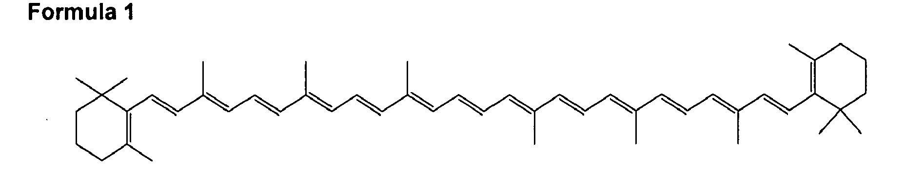
- the polyene-based pigment may include a compound represented by at least one of Formula 1 or Formula 2:
- the azo-based pigment may include a compound represented by Formula 3:
- the quinacridone-based pigment may include a compound represented by at least one of Formula 4 or Formula 5:
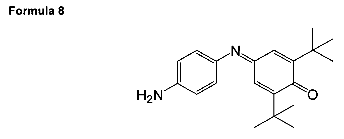
- the quinine-based pigment may include a compound represented by at least one of Formula 6, Formula 7, or Formula 8:
- the indigo-based pigment may include a compound represented by at least one of Formula 9, Formula 10, or Formula 11:
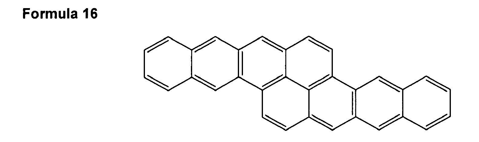
- the aromatic hydrocarbons may include a compound represented by at least one of Formula 12, Formula 13, Formula 14, Formula 15, Formula 16, Formula 17, or Formula 18:
- an organic light emitting diode (OLED) display as set out in claim 1.
- the filling agent can act as a filter.
- the filling agent is adapted to selectively absorb more light in a wavelength band of external light entering through the encapsulation substrate assembly than light in a wavelength band of emissive light emitted by the organic light emitting element. Preferred features of this aspect are set out in claims 2 to 15.
- the OLED display improves impact durability and at the same time improves visibility by suppressing reflection of external light, and a loss of light emitted to the outside from the organic light emitting element can be reduced (minimized).
- FIG. 1 is a cross-sectional view of an organic light emitting diode (OLED) display according to an illustrative embodiment.
- OLED organic light emitting diode
- FIG. 2 is an enlarged layout view of an internal structure of the OLED display of FIG. 1 .
- FIG. 3 is a cross-sectional view of FIG. 2 , taken along the line III-III.
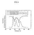
- FIG. 4 is a graph illustrating a transmittance distribution for each wavelength band of Experimental Example 1 and Experimental Example 2 according to embodiments of the present invention.
- an organic light emitting diode (OLED) display is illustrated as an active matrix (AM)-type OLED display in a 2Tr-1 Cap structure in which two TFTs T1 and T2 and one storage capacitor C1 are formed in one pixel, but the present invention is not limited thereto. Therefore, the OLED display according the embodiments of the present invention can have various suitable structures. For example, three or more TFTs and two or more capacitors can be provided in one pixel of the OLED display, and separate wires can be further provided in the OLED display.
- a pixel is a minimum unit for displaying an image, and the OLED display displays an image by using a plurality of pixels.
- FIGs. 1 , 2 , and 3 An illustrative embodiment will be described with reference to FIGs. 1 , 2 , and 3 .
- an organic light emitting diode (OLED) display 101 includes a display substrate assembly 110, an encapsulation substrate assembly 210, a sealant 350, and a filling agent 300.
- the display substrate assembly 110 includes a first substrate 111, a driving circuit (DC), and an organic light emitting element 70.
- the driving circuit DC and the organic light emitting element 70 are formed on the first substrate 111.
- the first substrate 111 may be formed of an insulating substrate made of glass, quartz, ceramic, and/or plastic. However, embodiments of the invention are not limited thereto, and the first substrate 111 may be formed of a metallic substrate made of stainless steel. Alternatively, other suitable materials could be used.
- the driving circuit DC includes thin film transistors 10 and 20 (shown in FIG. 2 ), and drives the organic light emitting element 70.
- the organic light emitting element 70 emits light according to a driving signal transmitted from the driving circuit DC to display images.
- FIG. 2 and FIG. 3 Detailed structures of the organic light emitting element 70 and the driving circuit DC are shown in FIG. 2 and FIG. 3 , but embodiments of the invention are not limited to the structures shown in FIG. 2 and FIG. 3 .
- the OLED 70 and the driving circuit may be suitably modified.
- wavelengths of more than 80% of light emitted from the organic light emitting element 70 are in wavelength ranges (bands) of 450nm to 480nm, of 510nm to 560 nm, and of 600nm to 650nm. That is, the organic light emitting element 70 mainly emits white light which is a mixture of light having wavelengths in the three wavelength ranges (bands).
- the encapsulation substrate assembly 210 is disposed at a distance from the display plate 110, and the encapsulation substrate assembly 210 and the display substrate assembly 110 are sealed, preferably in a vacuum-tight manner. As described, the encapsulation substrate assembly 210 sealed with the display substrate assembly 110 covers the organic light emitting element 70 and the driving circuit DC of the display substrate assembly 110 for protection.
- the encapsulation substrate assembly 210 includes a second substrate 211 made of a transparent material such as glass and plastic.
- the filling agent 300 is disposed between the display substrate assembly 110 and the encapsulation substrate assembly 210 to fill a space formed between the display substrate assembly 110 and the encapsulation substrate assembly 210. As described, the filling agent 300 improves mechanical strength by filling the space between the display substrate assembly 110 and the encapsulation substrate assembly 210. That is, the inside of the OLED display 101 is filled with the filling agent 300 so that durability to external impact can be improved.
- the filling agent 300 selectively absorbs external light incident upon the organic light emitting element 70 of the display substrate assembly 110 that has entered from the outside through the encapsulation substrate assembly 210 depending on (or as a function) the wavelength in the wavelength range (band) of the external light to control transmittance.
- the filling agent according to embodiments of the present invention can act as a filter that selectively absorbs external light entering through the encapsulation substrate assembly.
- the filling agent can be adapted to selectively absorb more light in a wavelength band of external light entering through the encapsulation substrate assembly than light in a wavelength band of emissive light emitted by the organic light emitting element.
- the filling agent 300 selectively absorbs external light in a wavelength range of 430nm to 670nm.
- the filling agent 300 absorbs a different amount of external light depending on (or as a function of) the wavelength in the wavelength range of 430nm to 670nm. That is, the filling agent 300 selectively absorbs the external light so that transmittance of the external light with respect to the filling agent 300 is changed depending of the wavelength of the external light within the wavelength range (band).
- a wavelength band-specific transmittance of the external light with respect to the filling agent 300 is higher in the wavelength range of 520nm to 560nm than in the wavelength range of 480nm to 510nm and the wavelength range of 580nm to 680nm.
- a graph illustrating the wavelength band-specific transmittance of the external light with respect to the filling agent 300 has a W-shape (like a quartic function) having two minimums and one maximum within a wavelength range of 460nm to 620nm.
- the two minimums are respectively located in a wavelength range of 480nm to 510nm and a wavelength range of 580nm to 610nm, and the maximum is located in a wavelength range of 520nm to 560nm.
- the filling agent 300 absorbs external light in a specific wavelength range (band) among external light that has entered through the encapsulation substrate assembly 210 and is incident upon the organic light emitting element 70 of the display substrate assembly 110 so as to suppress reflection of external light.
- the filling agent 300 absorbs some external light included in the wavelength range of 430nm to 670nm, and intensively absorbs external light included in the wavelength range of 580nm to 610nm.
- Emissive light of the organic light emitting element 70 is mainly included in wavelength ranges of 450nm to 480nm, 510nm to 560 nm, and 600nm to 650nm.
- the wavelengths of more than 80% of the emissive light of the organic light emitting element 70 are included in one or more specific wavelength bands (e.g., the above three described specific wavelength ranges (bands)), and the one or more specific wavelength bands (to which the wavelengths of most of the emissive light are included in) do not overlap to a significant degree with the wavelength bands where the transmittance of the external light with respect to the filling agent 300 is relatively low, which are in the wavelength ranges (bands) of 480nm to 510nm and of 580nm to 610nm. Therefore, compared to the external light, a loss of the emissive light of the organic light emitting element 70 when passing through the filling agent 300 is relatively low.
- the transmittance of the filling agent 300 is controlled to reduce or minimize absorption of emissive light of the organic light emitting element 70 and increase or maximize absorption of external light. That is, the filling agent 300 suppresses reflection of external light by absorbing a great amount of external light, but a relatively small amount of emissive light of the organic light emitting element 70, passing through the filling agent 300, is lost. Accordingly, the filling agent 300 can reduce or minimize a loss of light emitted outside from the organic light emitting element 70 while improving visibility by suppressing reflection of external light.
- the filling agent 300 includes a resin containing a light absorbing material.
- the external light transmittance by the filling agent 300 can be controlled according to the type and content of the light absorbing materials that are utilized.
- the resin includes polycarbonate, polyether sulfone (PES), polymethyl methacrylate, (PMMA), polyethylene terephthalate, and/or triacetate cellulose.
- the light absorbing material includes carbon black, a polyene-based pigment, an azo-based pigment, an azomethine-based pigment, a diimmonium-based pigment, a phthalocyanine-based pigment, a quinine-based pigment, an indigo-based pigment, a thioindigo-based pigment, a dioxadin-based pigment, a quinacridone-based pigment, an isoindolinone-based pigment, a metal oxide, a metal complex, and/or aromatic hydrocarbons.
- the light absorbing material absorbs light in a specific wavelength band according to the type thereof. Therefore, the filling agent 300 may have transmittance that is selective to a wavelength band of external light according to the light absorbing material included therein. That is, light transmittance can be intensively controlled in a specific wavelength band in consideration of external light of which reflection is to be suppressed and a main wavelength band of the emissive light of the organic light emitting element 70.
- the light absorbing material can be made of a combination of various suitable materials.
- the filling agent 300 can selectively control a transmittance of external light in a specific wavelength band by including one or two or more of light absorbing materials to be described hereinafter.
- the polyene-based pigment includes a compound represented by Formula 1 and/or Formula 2.
- the compound of Formula 1 is called dodecapreno-beta-carotene, and enables absorbing of light having a wavelength range of about 480nm to about 530nm.
- the compound of Formula 2 is called a trans-stilbene, and enables absorbing of light having a wavelength of about 525nm.
- the azo-based pigment includes a compound represented by Formula 3.
- the compound of Formula 3 enables absorbing of light having a wavelength of about 518nm.
- the quinacridone-based pigment includes a compound represented by Formula 4 and/or Formula 5.
- the compound of Formula 4 absorbs light having a wavelength of about 523nm
- the compound of Formula 5 absorbs light having a wavelength of about 528nm.
- the quinine-based pigment includes a compound represented by Formula 6, Formula 7, and/or Formula 8.
- the compound of Formula 6 absorbs light having a wavelength of about 528nm
- the compound of Formula 7 absorbs light having a wavelength of about 549nm
- the compound of Formula 8 absorbs light having a wavelength of about 508nm.
- the indigo-based pigment includes a compound represented by Formula 9, Formula 10, and/or Formula 11.
- the compound of Formula 9 absorbs light having a wavelength of about 546nm
- the compound of Formula 10 absorbs light having a wavelength of about 505nm
- the compound of Formula 11 absorbs light having a wavelength of about 534nm.
- the aromatic hydrocarbons include a compound represented by Formula 12, Formula 13, Formula 14, Formula 15, Formula 16, Formula 17, and/or Formula 18.
- the compound of Formula 12 absorbs light having a wavelength of about 523nm
- the compound of Formula 13 absorbs light having a wavelength of about 512nm
- the compound of Formula 14 absorbs light having a wavelength of about 510nm
- the compound of Formula 15 absorbs light having a wavelength of about 519nm.
- the compound of Formula 16 absorbs light having a wavelength of about 534nm
- the compound of Formula 17 absorbs light having a wavelength of about 523nm
- the compound of Formula 18 absorbs light having a wavelength of about 521 nm.
- the sealant 350 is disposed between edges or edge portions of the display substrate assembly 110 and the encapsulation substrate assembly 210 to seal them in a vacuum-tight manner. That is, the display substrate assembly 110 and the encapsulation substrate assembly 210 are sealed in a vacuum-tight manner by the sealant 350.
- the OLED display 101 can improve impact durability and at the same time improves visibility by suppressing reflection of external light, and loss of light emitted to the outside from the organic light emitting element 70 can be reduced or minimized. Therefore, use efficiency of overall light in the OLED display 101 is increased so that luminance can be improved.
- the OLED display 101 can reduce power consumption and have an increased life-span.
- FIG. 2 is a layout view of a pixel structure, focusing on the display substrate assembly 110
- FIG. 3 is a cross-sectional view of the display substrate assembly 110 and the encapsulation substrate assembly 210 of FIG. 2 , taken along the line III-III.
- the display substrate assembly 110 includes a switching thin film transistor 10, a driving thin film transistor 20, a capacitor 80, and an OLED 70, which are formed at each pixel.
- a configuration including the switching thin film transistor 10, the driving thin film transistor 20, and the capacitor 80 is referred to as a driving circuit DC.
- the display substrate assembly 110 further includes gate lines 151 arranged to extend in a first direction, and data lines 171 and common power lines 172 that extend in a second direction crossing the first direction of the gate lines 151 in an insulated manner.
- a pixel is defined by taking a gate line 151, a data line 171, and a common power line 172 as boundaries of the pixel, but the present invention is not limited thereto.
- the organic light emitting element 70 includes a pixel electrode 710, an organic emission layer 720 formed on the pixel electrode 710, and a common electrode 730 formed on the organic emission layer 730.
- the pixel electrode 710 functions as a positive (+) electrode that is utilized as a hole injection electrode
- the common electrode 730 functions as a negative (-) electrode that is utilized as an electron injection electrode.
- the present invention is not limited thereto, and depending upon the way of driving the OLED display 100, it is possible that the pixel electrode 710 functions as the negative electrode and the common electrode 730 functions as the positive electrode. Holes and electrons from the pixel electrode 710 and the common electrode 730 are injected into the organic emission layer 720. When excitons generated from combinations of electrons and holes shift from an excited state to a ground state, light emission occurs.
- the organic light emitting element 70 emits light toward a direction of the encapsulation substrate assembly 210. That is, the organic light emitting element 70 is formed as a front emission type.
- the pixel electrode 710 may be formed as a reflective electrode and the common electrode 730 may be formed as a transparent or semi-transparent electrode.
- the capacitor 80 includes a pair of capacitive plates 158 and 178, interposing an interlayer insulating layer 160 therebetween.
- the interlayer insulating layer 160 functions as a dielectric material. Capacitance is determined according to charges charged at the capacitor 80 and a voltage between the capacitive plates 158 and 178.
- the switching thin film transistor 10 includes a switching semiconductor layer 131, a switching gate electrode 152, a switching source electrode 173, and a switching drain electrode 174.
- the driving thin film transistor 20 includes a driving semiconductor layer 132, a driving gate electrode 155, a driving source electrode 176, and a driving drain electrode 177.
- the switching thin film transistor 10 is used as a switch for selecting a pixel to emit light.
- the switching gate electrode 152 is connected to a gate line 151.
- the switching source electrode 173 is connected to a data line 171.
- the switching drain electrode 174 is disposed at a distance from the switching source electrode 173 and is connected to one of the capacitive plates, for example, the capacitive plate 158.
- the driving thin film transistor 20 applies a driving voltage to a pixel electrode 710 to excite an organic emission layer 720 of an organic light emitting element 70 in the selected pixel.
- the driving gate electrode 155 is connected to the capacitive plate 158 connected to the switching drain electrode 174.
- the driving source electrode 176 and the other capacitive plate 178 are respectively connected to a common power line 172.
- the driving drain electrode 177 is connected to the pixel electrode 710 of the organic light emitting element 70 through a contact hole.
- the switching thin film transistor 10 is operated by the gate voltage applied to the gate line 161, and transmits the data voltage applied to the data line 171 to the driving thin film transistor 20.
- the voltage with a value corresponding to a difference between the common voltage applied to the driving thin film transistor 20 from the common power line 172 and the data voltage transmitted from the switching thin film transistor 10 is stored at the capacitor 80, and the current corresponding to the voltage stored at the capacitor 80 flows to the organic light emitting element 70 through the driving thin film transistor 20 to thereby excite the OLED 70 to emit light.
- the encapsulation substrate assembly 210 is disposed on the organic light emitting element 70 for protecting the encapsulation substrate assembly 210.
- the filling agent 300 is filled between the display substrate assembly 110 and the encapsulation substrate assembly 210.
- Experimental Example 1 and Experimental Example 2 were performed with different types and contents of a light absorbing material included in the filling agent 300.
- the Experimental Example 1 and Experimental Example 2 both have W-type graphs for wavelength band-specific transmittance of external light through the filling agent.
- the band-specific transmittance of external light through the filling agent is higher in a range other than the ranges of 480nm to 510nm and 580nm to 680nm.
- a wavelength of an emissive light of the OLED according to the illustrative embodiment is mainly included within the wavelength ranges of 450nm to 480nm, 510nm to 560 nm, and 600nm to 650nm.
- the filling agent absorbs most of the external light but a loss of the emissive light of the OLED passing through the filling agent is relatively small. That is, both of the Experimental Example 1 and Experimental Example 2 suppress reflection of external light while reducing or minimizing a loss of light emitted to the outside from the OLED.
- a typical filling agent that does not have a selective light absorbing function has a transmittance range of 0.9 to 1, and has a straight line-type graph for wavelength band-specific transmittance of external light through the typical filling agent. Therefore, the conventional typical filling agent cannot suppress reflection of external light.
- the filling agent according to embodiments of the present invention can act as a filter that selectively absorbs external light entering through the encapsulation substrate assembly, a conventional filling agent does not act in this way.
Landscapes
- Physics & Mathematics (AREA)
- Optics & Photonics (AREA)
- General Physics & Mathematics (AREA)
- Electroluminescent Light Sources (AREA)
- Devices For Indicating Variable Information By Combining Individual Elements (AREA)
- Optical Filters (AREA)
Abstract
Description
- The present invention relates to an organic light emitting diode (OLED) display. More particularly, the present invention relates to an OLED display of which impact durability and display characteristics are improved.
- An organic light emitting diode (OLED) display is an emissive or self-luminance display, and differs from a liquid crystal display (LCD) in that it does not require a separate light source so that it can be made to be relatively thin and light in weight. Furthermore, as the OLED display has characteristics such as relatively low power consumption, high luminance, and short response time, it has been spotlighted as a next generation display device.
- In the OLED display, the hole injection electrodes or the electron injection electrodes of the OLED display, and other various metal wires thereof, reflect light that is incident thereupon from the outside. When the OLED display is used in a bright location, the black color expression and the contrast thereof may be poor due to the reflection of external light.
- In order to reduce the reflection of external light, a polarizing plate and a phase delay plate may be utilized in an OLED display for suppressing reflection of the external light. However, a conventional method that suppresses reflection of external light through the polarizing plate and the phase delay plate has a problem in that a large amount of light generated from an organic emission layer can also be lost when the light is emitted to the outside through the polarizing plate and the phase delay plate.
- The above information disclosed in this Background section is only for enhancement of understanding of the background of the described technology and therefore it may contain information that does not form the prior art that is already known in this country to a person of ordinary skill in the art.
- Some embodiments of the present invention are directed toward an OLED display having improved impact durability and ability to suppress reflection of external light to thereby improve visibility and reduce (minimize) a loss of light emitted to the outside from an organic light emitting element in the OLED display.
- An organic light emitting diode (OLED) display according to one aspect of the present invention includes: a display substrate assembly including an organic light emitting element; an encapsulation substrate assembly on the display substrate assembly with a space therebetween, the encapsulation substrate assembly being sealed with the display substrate assembly; and a filling agent filling the space between the display substrate assembly and the encapsulation substrate assembly. Here, the filling agent is adapted to selectively absorb external light entering through the encapsulation substrate assembly and incident on the organic light emitting element as a function of wavelength in a wavelength band of the external light to control transmittance.
- The filling agent may be adapted to selectively absorb the external light having wavelengths in a wavelength band of from 430nm to 670nm.
- The transmittance of the external light with respect to the filling agent may be higher in a wavelength band of from 520nm to 560nm than in wavelength bands of from 480nm to 510nm and of from 580nm to 610nm.
- The transmittance of the external light with respect to the filling agent in a wavelength band of from 460nm to 620nm may satisfy a W shape like a quartic function having two minimums and one maximum.
- The two minimums may be respectively in the wavelength band of from 480nm to 510nm and the wavelength band of from 580nm to 610nm, and the maximum may be in the wavelength band of from 520nm to 560nm.
- Wavelengths of more than 80% of emissive light of the organic light emitting element may be in one or more specific wavelength bands, and the one or more specific wavelength bands may not be overlapped with the wavelength bands of from 480nm to 510nm and of from 580nm to 610nm.
- The wavelengths of more than 80% of the emissive light of the organic light emitting element may be in the wavelength bands of from 450nm to 480nm, of from 510nm to 560 nm, and of from 600nm to 650nm.
- The filling agent may include a resin containing a light absorbing material.
- The transmittance of the external light by the filling agent may be controlled according to the type and content of the light absorbing material.
- The resin may include at least one of polycarbonate, polyether sulfone (PES), polymethyl methacrylate, (PMMA), polyethylene terephthalate, or triacetate cellulose.
- The light absorbing material may include at least one of carbon black, a polyene-based pigment, an azo-based pigment, an azomethine-based pigment, a diimmonium-based pigment, a phthalocyanine-based pigment, a quinine-based pigment, an indigo-based pigment, a thioindigo-based pigment, a dioxadin-based pigment, a quinacridone-based pigment, an isoindolinone-based pigment, a metal oxide, a metal complex, or aromatic hydrocarbons.
- The polyene-based pigment may include a compound represented by at least one of Formula 1 or Formula 2:

- The azo-based pigment may include a compound represented by Formula 3:

- The quinacridone-based pigment may include a compound represented by at least one of Formula 4 or Formula 5:


- The quinine-based pigment may include a compound represented by at least one of Formula 6, Formula 7, or Formula 8:


- The indigo-based pigment may include a compound represented by at least one of Formula 9, Formula 10, or Formula 11:


- The aromatic hydrocarbons may include a compound represented by at least one of Formula 12, Formula 13, Formula 14, Formula 15, Formula 16, Formula 17, or Formula 18:




- According to an aspect of the present invention, there is provided an organic light emitting diode (OLED) display as set out in claim 1. As a result, the filling agent can act as a filter. In some embodiments, the filling agent is adapted to selectively absorb more light in a wavelength band of external light entering through the encapsulation substrate assembly than light in a wavelength band of emissive light emitted by the organic light emitting element. Preferred features of this aspect are set out in
claims 2 to 15. - According to some embodiments of the present invention, the OLED display improves impact durability and at the same time improves visibility by suppressing reflection of external light, and a loss of light emitted to the outside from the organic light emitting element can be reduced (minimized).
-
FIG. 1 is a cross-sectional view of an organic light emitting diode (OLED) display according to an illustrative embodiment. -
FIG. 2 is an enlarged layout view of an internal structure of the OLED display ofFIG. 1 . -
FIG. 3 is a cross-sectional view ofFIG. 2 , taken along the line III-III. -
FIG. 4 is a graph illustrating a transmittance distribution for each wavelength band of Experimental Example 1 and Experimental Example 2 according to embodiments of the present invention. - In the following detailed description, only certain illustrative embodiments of the present invention are shown and described. As those skilled in the art would recognize, the invention may be embodied in many different forms and should not be construed as being limited to the embodiments set forth herein. Also, in the context of the present application, when a first element is referred to as being "on" a second element, it can be directly on the second element or be indirectly on the second element with one or more intervening elements interposed therebetween. Like reference numerals designate like elements throughout the specification.
- In addition, in
FIG. 2 andFIG. 3 , an organic light emitting diode (OLED) display is illustrated as an active matrix (AM)-type OLED display in a 2Tr-1 Cap structure in which two TFTs T1 and T2 and one storage capacitor C1 are formed in one pixel, but the present invention is not limited thereto. Therefore, the OLED display according the embodiments of the present invention can have various suitable structures. For example, three or more TFTs and two or more capacitors can be provided in one pixel of the OLED display, and separate wires can be further provided in the OLED display. Here, a pixel is a minimum unit for displaying an image, and the OLED display displays an image by using a plurality of pixels. - Hereinafter, an illustrative embodiment will be described with reference to
FIGs. 1 ,2 , and3 . - As shown in
FIG. 1 , an organic light emitting diode (OLED)display 101 according to an illustrative embodiment includes adisplay substrate assembly 110, anencapsulation substrate assembly 210, asealant 350, and afilling agent 300. - The
display substrate assembly 110 includes afirst substrate 111, a driving circuit (DC), and an organiclight emitting element 70. The driving circuit DC and the organiclight emitting element 70 are formed on thefirst substrate 111. - The
first substrate 111 may be formed of an insulating substrate made of glass, quartz, ceramic, and/or plastic. However, embodiments of the invention are not limited thereto, and thefirst substrate 111 may be formed of a metallic substrate made of stainless steel. Alternatively, other suitable materials could be used. - The driving circuit DC includes
thin film transistors 10 and 20 (shown inFIG. 2 ), and drives the organiclight emitting element 70. The organiclight emitting element 70 emits light according to a driving signal transmitted from the driving circuit DC to display images. - Detailed structures of the organic
light emitting element 70 and the driving circuit DC are shown inFIG. 2 andFIG. 3 , but embodiments of the invention are not limited to the structures shown inFIG. 2 andFIG. 3 . The OLED 70 and the driving circuit may be suitably modified. - Also, in the illustrative embodiment, wavelengths of more than 80% of light emitted from the organic
light emitting element 70 are in wavelength ranges (bands) of 450nm to 480nm, of 510nm to 560 nm, and of 600nm to 650nm. That is, the organiclight emitting element 70 mainly emits white light which is a mixture of light having wavelengths in the three wavelength ranges (bands). - The
encapsulation substrate assembly 210 is disposed at a distance from thedisplay plate 110, and theencapsulation substrate assembly 210 and thedisplay substrate assembly 110 are sealed, preferably in a vacuum-tight manner. As described, theencapsulation substrate assembly 210 sealed with thedisplay substrate assembly 110 covers the organiclight emitting element 70 and the driving circuit DC of thedisplay substrate assembly 110 for protection. Theencapsulation substrate assembly 210 includes asecond substrate 211 made of a transparent material such as glass and plastic. - The filling
agent 300 is disposed between thedisplay substrate assembly 110 and theencapsulation substrate assembly 210 to fill a space formed between thedisplay substrate assembly 110 and theencapsulation substrate assembly 210. As described, the fillingagent 300 improves mechanical strength by filling the space between thedisplay substrate assembly 110 and theencapsulation substrate assembly 210. That is, the inside of theOLED display 101 is filled with the fillingagent 300 so that durability to external impact can be improved. - In addition, the filling
agent 300 selectively absorbs external light incident upon the organiclight emitting element 70 of thedisplay substrate assembly 110 that has entered from the outside through theencapsulation substrate assembly 210 depending on (or as a function) the wavelength in the wavelength range (band) of the external light to control transmittance. In other words, the filling agent according to embodiments of the present invention can act as a filter that selectively absorbs external light entering through the encapsulation substrate assembly. In particular, the filling agent can be adapted to selectively absorb more light in a wavelength band of external light entering through the encapsulation substrate assembly than light in a wavelength band of emissive light emitted by the organic light emitting element. - In the illustrative embodiment, the filling
agent 300 selectively absorbs external light in a wavelength range of 430nm to 670nm. In particular, the fillingagent 300 absorbs a different amount of external light depending on (or as a function of) the wavelength in the wavelength range of 430nm to 670nm. That is, the fillingagent 300 selectively absorbs the external light so that transmittance of the external light with respect to the fillingagent 300 is changed depending of the wavelength of the external light within the wavelength range (band). - In further detail, a wavelength band-specific transmittance of the external light with respect to the filling
agent 300 is higher in the wavelength range of 520nm to 560nm than in the wavelength range of 480nm to 510nm and the wavelength range of 580nm to 680nm. - That is, a graph illustrating the wavelength band-specific transmittance of the external light with respect to the filling
agent 300 has a W-shape (like a quartic function) having two minimums and one maximum within a wavelength range of 460nm to 620nm. Here, the two minimums are respectively located in a wavelength range of 480nm to 510nm and a wavelength range of 580nm to 610nm, and the maximum is located in a wavelength range of 520nm to 560nm. As described, the fillingagent 300 absorbs external light in a specific wavelength range (band) among external light that has entered through theencapsulation substrate assembly 210 and is incident upon the organiclight emitting element 70 of thedisplay substrate assembly 110 so as to suppress reflection of external light. The fillingagent 300 absorbs some external light included in the wavelength range of 430nm to 670nm, and intensively absorbs external light included in the wavelength range of 580nm to 610nm. - Emissive light of the organic
light emitting element 70 is mainly included in wavelength ranges of 450nm to 480nm, 510nm to 560 nm, and 600nm to 650nm. Here, as described above, the wavelengths of more than 80% of the emissive light of the organiclight emitting element 70 are included in one or more specific wavelength bands (e.g., the above three described specific wavelength ranges (bands)), and the one or more specific wavelength bands (to which the wavelengths of most of the emissive light are included in) do not overlap to a significant degree with the wavelength bands where the transmittance of the external light with respect to the fillingagent 300 is relatively low, which are in the wavelength ranges (bands) of 480nm to 510nm and of 580nm to 610nm. Therefore, compared to the external light, a loss of the emissive light of the organiclight emitting element 70 when passing through the fillingagent 300 is relatively low. - As described, the transmittance of the filling
agent 300 is controlled to reduce or minimize absorption of emissive light of the organiclight emitting element 70 and increase or maximize absorption of external light. That is, the fillingagent 300 suppresses reflection of external light by absorbing a great amount of external light, but a relatively small amount of emissive light of the organiclight emitting element 70, passing through the fillingagent 300, is lost. Accordingly, the fillingagent 300 can reduce or minimize a loss of light emitted outside from the organiclight emitting element 70 while improving visibility by suppressing reflection of external light. - In addition, the filling
agent 300 includes a resin containing a light absorbing material. The external light transmittance by the fillingagent 300 can be controlled according to the type and content of the light absorbing materials that are utilized. - Here, in one embodiment, the resin includes polycarbonate, polyether sulfone (PES), polymethyl methacrylate, (PMMA), polyethylene terephthalate, and/or triacetate cellulose.
- The light absorbing material includes carbon black, a polyene-based pigment, an azo-based pigment, an azomethine-based pigment, a diimmonium-based pigment, a phthalocyanine-based pigment, a quinine-based pigment, an indigo-based pigment, a thioindigo-based pigment, a dioxadin-based pigment, a quinacridone-based pigment, an isoindolinone-based pigment, a metal oxide, a metal complex, and/or aromatic hydrocarbons.
- The light absorbing material absorbs light in a specific wavelength band according to the type thereof. Therefore, the filling
agent 300 may have transmittance that is selective to a wavelength band of external light according to the light absorbing material included therein. That is, light transmittance can be intensively controlled in a specific wavelength band in consideration of external light of which reflection is to be suppressed and a main wavelength band of the emissive light of the organiclight emitting element 70. In this case, the light absorbing material can be made of a combination of various suitable materials. - Some of light absorbing materials that can be included in the filling
agent 300 will be exemplarily described in further detail. The fillingagent 300 can selectively control a transmittance of external light in a specific wavelength band by including one or two or more of light absorbing materials to be described hereinafter. - In one embodiment, the polyene-based pigment includes a compound represented by Formula 1 and/or
Formula 2.

- Here, the compound of Formula 1 is called dodecapreno-beta-carotene, and enables absorbing of light having a wavelength range of about 480nm to about 530nm. The compound of
Formula 2 is called a trans-stilbene, and enables absorbing of light having a wavelength of about 525nm. - In one embodiment, the azo-based pigment includes a compound represented by Formula 3.

- Here, the compound of Formula 3 enables absorbing of light having a wavelength of about 518nm.
- In one embodiment, the quinacridone-based pigment includes a compound represented by Formula 4 and/or Formula 5.


- Here, the compound of Formula 4 absorbs light having a wavelength of about 523nm, and the compound of Formula 5 absorbs light having a wavelength of about 528nm.
- In one embodiment, the quinine-based pigment includes a compound represented by Formula 6, Formula 7, and/or Formula 8.


- Here, the compound of Formula 6 absorbs light having a wavelength of about 528nm, the compound of Formula 7 absorbs light having a wavelength of about 549nm, and the compound of Formula 8 absorbs light having a wavelength of about 508nm.
- In one embodiment, the indigo-based pigment includes a compound represented by Formula 9,
Formula 10, and/or Formula 11.
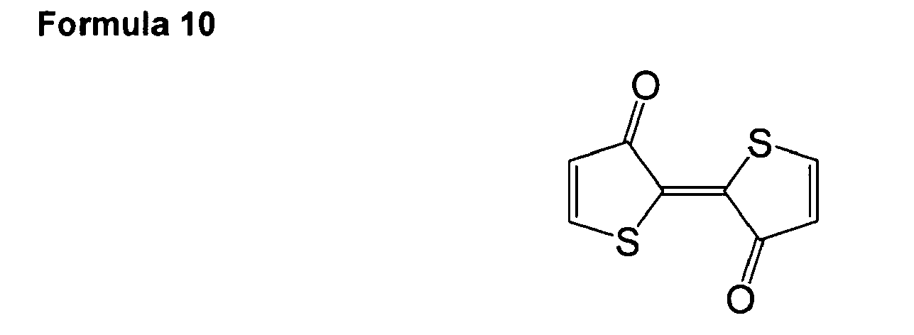

- Here, the compound of Formula 9 absorbs light having a wavelength of about 546nm, the compound of
Formula 10 absorbs light having a wavelength of about 505nm, and the compound of Formula 11 absorbs light having a wavelength of about 534nm. - In one embodiment, the aromatic hydrocarbons include a compound represented by Formula 12, Formula 13, Formula 14, Formula 15, Formula 16, Formula 17, and/or Formula 18.


- Here, the compound of Formula 12 absorbs light having a wavelength of about 523nm, and the compound of Formula 13 absorbs light having a wavelength of about 512nm. The compound of Formula 14 absorbs light having a wavelength of about 510nm, and the compound of Formula 15 absorbs light having a wavelength of about 519nm. The compound of Formula 16 absorbs light having a wavelength of about 534nm, the compound of Formula 17 absorbs light having a wavelength of about 523nm, and the compound of Formula 18 absorbs light having a wavelength of about 521 nm.
- The
sealant 350 is disposed between edges or edge portions of thedisplay substrate assembly 110 and theencapsulation substrate assembly 210 to seal them in a vacuum-tight manner. That is, thedisplay substrate assembly 110 and theencapsulation substrate assembly 210 are sealed in a vacuum-tight manner by thesealant 350. - With the above-described configuration, the
OLED display 101 can improve impact durability and at the same time improves visibility by suppressing reflection of external light, and loss of light emitted to the outside from the organiclight emitting element 70 can be reduced or minimized. Therefore, use efficiency of overall light in theOLED display 101 is increased so that luminance can be improved. - In addition, the
OLED display 101 can reduce power consumption and have an increased life-span. - Hereinafter, an internal structure of the
OLED display 101 will be described in further detail with reference toFIG. 2 andFIG. 3 .FIG. 2 is a layout view of a pixel structure, focusing on thedisplay substrate assembly 110, andFIG. 3 is a cross-sectional view of thedisplay substrate assembly 110 and theencapsulation substrate assembly 210 ofFIG. 2 , taken along the line III-III. - As shown in
FIG. 2 andFIG. 3 , thedisplay substrate assembly 110 includes a switchingthin film transistor 10, a drivingthin film transistor 20, acapacitor 80, and anOLED 70, which are formed at each pixel. Here, a configuration including the switchingthin film transistor 10, the drivingthin film transistor 20, and thecapacitor 80 is referred to as a driving circuit DC. In addition, thedisplay substrate assembly 110 further includesgate lines 151 arranged to extend in a first direction, anddata lines 171 andcommon power lines 172 that extend in a second direction crossing the first direction of thegate lines 151 in an insulated manner. Here, a pixel is defined by taking agate line 151, adata line 171, and acommon power line 172 as boundaries of the pixel, but the present invention is not limited thereto. - The organic
light emitting element 70 includes apixel electrode 710, anorganic emission layer 720 formed on thepixel electrode 710, and acommon electrode 730 formed on theorganic emission layer 730. Thepixel electrode 710 functions as a positive (+) electrode that is utilized as a hole injection electrode, and thecommon electrode 730 functions as a negative (-) electrode that is utilized as an electron injection electrode. However, the present invention is not limited thereto, and depending upon the way of driving the OLED display 100, it is possible that thepixel electrode 710 functions as the negative electrode and thecommon electrode 730 functions as the positive electrode. Holes and electrons from thepixel electrode 710 and thecommon electrode 730 are injected into theorganic emission layer 720. When excitons generated from combinations of electrons and holes shift from an excited state to a ground state, light emission occurs. - In the
OLED display 101 according to an illustrative embodiment, the organiclight emitting element 70 emits light toward a direction of theencapsulation substrate assembly 210. That is, the organiclight emitting element 70 is formed as a front emission type. For light emission of the organiclight emitting element 70 toward theencapsulation substrate assembly 210 direction, thepixel electrode 710 may be formed as a reflective electrode and thecommon electrode 730 may be formed as a transparent or semi-transparent electrode. - The
capacitor 80 includes a pair ofcapacitive plates interlayer insulating layer 160 therebetween. Here, theinterlayer insulating layer 160 functions as a dielectric material. Capacitance is determined according to charges charged at thecapacitor 80 and a voltage between thecapacitive plates - The switching
thin film transistor 10 includes a switchingsemiconductor layer 131, a switching gate electrode 152, a switching source electrode 173, and aswitching drain electrode 174. The drivingthin film transistor 20 includes a drivingsemiconductor layer 132, a drivinggate electrode 155, a drivingsource electrode 176, and a drivingdrain electrode 177. - The switching
thin film transistor 10 is used as a switch for selecting a pixel to emit light. The switching gate electrode 152 is connected to agate line 151. The switching source electrode 173 is connected to adata line 171. The switchingdrain electrode 174 is disposed at a distance from the switching source electrode 173 and is connected to one of the capacitive plates, for example, thecapacitive plate 158. - The driving
thin film transistor 20 applies a driving voltage to apixel electrode 710 to excite anorganic emission layer 720 of an organiclight emitting element 70 in the selected pixel. The drivinggate electrode 155 is connected to thecapacitive plate 158 connected to theswitching drain electrode 174. The drivingsource electrode 176 and theother capacitive plate 178 are respectively connected to acommon power line 172. The drivingdrain electrode 177 is connected to thepixel electrode 710 of the organiclight emitting element 70 through a contact hole. - With the above structure, the switching
thin film transistor 10 is operated by the gate voltage applied to the gate line 161, and transmits the data voltage applied to thedata line 171 to the drivingthin film transistor 20. The voltage with a value corresponding to a difference between the common voltage applied to the drivingthin film transistor 20 from thecommon power line 172 and the data voltage transmitted from the switchingthin film transistor 10 is stored at thecapacitor 80, and the current corresponding to the voltage stored at thecapacitor 80 flows to the organiclight emitting element 70 through the drivingthin film transistor 20 to thereby excite theOLED 70 to emit light. - As shown in
FIG. 3 , theencapsulation substrate assembly 210 is disposed on the organiclight emitting element 70 for protecting theencapsulation substrate assembly 210. In addition, the fillingagent 300 is filled between thedisplay substrate assembly 110 and theencapsulation substrate assembly 210. - Hereinafter, referring to
FIG. 4 , an effect of embodiments of the present invention will be described in further detail through Experimental Example 1 and Experimental Example 2. Experimental Example 1 and Experimental Example 2 were performed with different types and contents of a light absorbing material included in the fillingagent 300. - As shown in
FIG. 4 , the Experimental Example 1 and Experimental Example 2 both have W-type graphs for wavelength band-specific transmittance of external light through the filling agent. In addition, the band-specific transmittance of external light through the filling agent is higher in a range other than the ranges of 480nm to 510nm and 580nm to 680nm. - In addition, as shown in
FIG. 4 , a wavelength of an emissive light of the OLED according to the illustrative embodiment is mainly included within the wavelength ranges of 450nm to 480nm, 510nm to 560 nm, and 600nm to 650nm. - Therefore, according to the Experimental Example 1 and Experimental Example 2, the filling agent absorbs most of the external light but a loss of the emissive light of the OLED passing through the filling agent is relatively small. That is, both of the Experimental Example 1 and Experimental Example 2 suppress reflection of external light while reducing or minimizing a loss of light emitted to the outside from the OLED.
- However, compared to the Experimental Example 1 and Experimental Example 2, a typical filling agent that does not have a selective light absorbing function has a transmittance range of 0.9 to 1, and has a straight line-type graph for wavelength band-specific transmittance of external light through the typical filling agent. Therefore, the conventional typical filling agent cannot suppress reflection of external light. In other words, whereas the filling agent according to embodiments of the present invention can act as a filter that selectively absorbs external light entering through the encapsulation substrate assembly, a conventional filling agent does not act in this way.
- While the present invention has been described in connection with certain exemplary embodiments, it is to be understood that the invention is not limited to the disclosed embodiments, but, on the contrary, is intended to cover various modifications and equivalent arrangements included within the scope of the appended claims, and equivalents thereof.
Claims (15)
- An organic light emitting diode (OLED) display comprising:a display substrate assembly comprising an organic light emitting element;an encapsulation substrate assembly on the display substrate assembly with a space therebetween, the encapsulation substrate assembly being sealed with the display substrate assembly; anda filling agent provided within the space between the display substrate assembly and the encapsulation substrate assembly,wherein the filling agent is adapted to selectively absorb external light entering through the encapsulation substrate assembly.
- An OLED display according to claim 1, wherein the filling agent is adapted to selectively absorb external light as a function of wavelength in a wavelength band of the external light to control transmittance.
- An OLED display according to claim 1 or 2, wherein the filling agent is adapted to selectively absorb more light in a wavelength band of external light entering through the encapsulation substrate assembly than light in a wavelength band of emissive light emitted by the organic light emitting element.
- An OLED display of according to any one of claims 1 to 3, wherein the transmittance of light with respect to the filling agent is higher in the wavelength bands of from 450nm to 480nm, of from 510nm to 560 nm, and of from 600nm to 650nm than in wavelength bands of from 480nm to 510nm and of from 580nm to 610nm.
- An OLED display according to any one of claims 1 to 4, wherein the filling agent is adapted to selectively absorb the external light having wavelengths in a wavelength band of from 430nm to 670nm.
- An OLED display according to any one of claims 1 to 5, wherein the transmittance of the external light with respect to the filling agent is higher in a wavelength band of from 520nm to 560nm than in wavelength bands of from 480nm to 510nm and of from 580nm to 610nm.
- An OLED display according to any preceding claim, wherein the transmittance of the external light with respect to the filling agent in a wavelength band of from 460nm to 620nm varies in a W shape and has two minimums and one maximum.
- An OLED display according to claim 7, wherein the two minimums are respectively in the wavelength band of from 480nm to 510nm and the wavelength band of from 580nm to 610nm, and the maximum is in the wavelength band of from 520nm to 560nm.
- An OLED display according to any of claims 6 to 8, wherein wavelengths of more than 80% of emissive light of the organic light emitting element are in one or more specific wavelength bands, and the one or more specific wavelength bands do not overlap with the wavelength bands of from 480nm to 510nm and of from 580nm to 610nm.
- An OLED display according to claim 6, wherein the wavelengths of more than 80% of the emissive light of the organic light emitting element are in the wavelength bands of from 450nm to 480nm, of from 510nm to 560 nm, and of from 600nm to 650nm.
- An OLED display according to any preceding claim, wherein the filling agent comprises a resin containing a light absorbing material.
- An OLED display according to claim 11, wherein the transmittance of the external light by the filling agent is controlled according to the type and content of the light absorbing material.
- An OLED display according to claim 11 or 12, wherein the resin comprises at least one of polycarbonate, polyether sulfone (PES), polymethyl methacrylate, (PMMA), polyethylene terephthalate, or triacetate cellulose.
- An OLED display according to any one of claims 11 to 13, wherein the light absorbing material comprises at least one of carbon black, a polyene-based pigment, an azo-based pigment, an azomethine-based pigment, a diimmonium-based pigment, a phthalocyanine-based pigment, a quinine-based pigment, an indigo-based pigment, a thioindigo-based pigment, a dioxadin-based pigment, a quinacridone-based pigment, an isoindolinone-based pigment, a metal oxide, a metal complex, or aromatic hydrocarbons.
- An OLED display according to claim 14, wherein the polyene-based pigment comprises a compound represented by at least one of Formula 1 or Formula 2:


Applications Claiming Priority (1)
| Application Number | Priority Date | Filing Date | Title |
|---|---|---|---|
| KR1020090069059A KR101065403B1 (en) | 2009-07-28 | 2009-07-28 | Organic light emitting display |
Publications (3)
| Publication Number | Publication Date |
|---|---|
| EP2284924A2 true EP2284924A2 (en) | 2011-02-16 |
| EP2284924A3 EP2284924A3 (en) | 2014-02-26 |
| EP2284924B1 EP2284924B1 (en) | 2018-09-19 |
Family
ID=43015798
Family Applications (1)
| Application Number | Title | Priority Date | Filing Date |
|---|---|---|---|
| EP10251340.5A Active EP2284924B1 (en) | 2009-07-28 | 2010-07-28 | Organic light emitting diode display |
Country Status (4)
| Country | Link |
|---|---|
| US (1) | US9112179B2 (en) |
| EP (1) | EP2284924B1 (en) |
| JP (2) | JP2011029165A (en) |
| KR (1) | KR101065403B1 (en) |
Families Citing this family (14)
| Publication number | Priority date | Publication date | Assignee | Title |
|---|---|---|---|---|
| KR20120120710A (en) * | 2011-04-25 | 2012-11-02 | 삼성디스플레이 주식회사 | Display device and method for manufacturing the same |
| KR102021027B1 (en) * | 2013-02-28 | 2019-09-16 | 삼성디스플레이 주식회사 | Organic luminescence emitting display device |
| JP6139196B2 (en) * | 2013-03-15 | 2017-05-31 | 株式会社ジャパンディスプレイ | ORGANIC ELECTROLUMINESCENT DISPLAY DEVICE AND METHOD FOR PRODUCING ORGANIC ELECTROLUMINESCENT DISPLAY DEVICE |
| JP6409771B2 (en) * | 2013-06-28 | 2018-10-24 | コニカミノルタ株式会社 | Organic electroluminescence device and method for manufacturing the same |
| KR102184673B1 (en) | 2013-08-14 | 2020-12-01 | 삼성디스플레이 주식회사 | Organic light emitting display apparatus and method of manufacturing organic light emitting display apparatus |
| JP2015088514A (en) * | 2013-10-28 | 2015-05-07 | 日東電工株式会社 | Resin sheet for sealing electronic device, and method of manufacturing electronic device package |
| KR20150097359A (en) * | 2014-02-18 | 2015-08-26 | 주식회사 엘지화학 | Encapsulation film and organic electronic device comprising the same |
| KR102238701B1 (en) * | 2015-02-03 | 2021-04-08 | 주식회사 엘지화학 | Electroactive material |
| JP6543998B2 (en) * | 2015-03-30 | 2019-07-17 | 大日本印刷株式会社 | LED BACKLIGHT AND LED DISPLAY USING THE SAME |
| JP6401650B2 (en) | 2015-03-31 | 2018-10-10 | 住友化学株式会社 | OLED display device and manufacturing method thereof |
| KR101702570B1 (en) * | 2015-10-30 | 2017-02-03 | 엘지디스플레이 주식회사 | Transparent Organic Light Emitting Display Device |
| JP7088351B1 (en) | 2021-03-12 | 2022-06-21 | 凸版印刷株式会社 | Optical film and display device |
| JP7248058B2 (en) | 2021-07-07 | 2023-03-29 | 凸版印刷株式会社 | optical film and display |
| JP7248057B2 (en) | 2021-07-07 | 2023-03-29 | 凸版印刷株式会社 | optical film and display |
Family Cites Families (38)
| Publication number | Priority date | Publication date | Assignee | Title |
|---|---|---|---|---|
| JPS6196695A (en) * | 1984-10-18 | 1986-05-15 | 松下電器産業株式会社 | El panel |
| US4802873A (en) * | 1987-10-05 | 1989-02-07 | Planar Systems, Inc. | Method of encapsulating TFEL panels with a curable resin |
| JP3246053B2 (en) | 1993-04-02 | 2002-01-15 | 東洋インキ製造株式会社 | Organic electroluminescence device |
| JPH07272848A (en) | 1994-03-29 | 1995-10-20 | Nippondenso Co Ltd | Electroluminescent element |
| JP2947106B2 (en) | 1994-12-08 | 1999-09-13 | 株式会社デンソー | Electroluminescence device and method of manufacturing the same |
| JPH09115664A (en) | 1995-10-17 | 1997-05-02 | Citizen Watch Co Ltd | Organic electroluminescent device |
| KR100384291B1 (en) | 2001-02-24 | 2003-05-16 | 주식회사 엘리아테크 | Organic electro luminescence display element with low reflectivity of cathode |
| JP4024526B2 (en) | 2001-08-29 | 2007-12-19 | 富士フイルム株式会社 | Fused octacyclic aromatic compound and organic EL device and organic EL display using the same |
| KR100459175B1 (en) | 2001-12-20 | 2004-12-03 | 엘지전자 주식회사 | sealing method of organic electroluminescence device |
| JP2003257622A (en) | 2002-02-28 | 2003-09-12 | Fuji Electric Co Ltd | Organic EL display and manufacturing method thereof |
| TWI314947B (en) * | 2002-04-24 | 2009-09-21 | Eastman Kodak Compan | Organic light emitting diode devices with improved operational stability |
| JPWO2003101155A1 (en) | 2002-05-23 | 2005-10-20 | 富士電機ホールディングス株式会社 | Organic EL display |
| JP2004241134A (en) | 2003-02-03 | 2004-08-26 | Seiko Epson Corp | Organic EL device and electronic equipment |
| US6998776B2 (en) * | 2003-04-16 | 2006-02-14 | Corning Incorporated | Glass package that is hermetically sealed with a frit and method of fabrication |
| WO2004112436A1 (en) | 2003-06-13 | 2004-12-23 | Fuji Electric Holdings Co., Ltd. | Organic el display and method for producing the same |
| US7384694B2 (en) | 2003-09-12 | 2008-06-10 | Ppg Industries Ohio, Inc. | Coating composition with flourescent colorants having color effect dependent on light intensity |
| US7314785B2 (en) | 2003-10-24 | 2008-01-01 | Semiconductor Energy Laboratory Co., Ltd. | Display device and manufacturing method thereof |
| KR100553758B1 (en) | 2004-02-02 | 2006-02-20 | 삼성에스디아이 주식회사 | Organic electroluminescent element |
| KR100637179B1 (en) | 2004-10-20 | 2006-10-23 | 삼성에스디아이 주식회사 | Organic electroluminescent display |
| JP2006127815A (en) | 2004-10-26 | 2006-05-18 | Sekisui Chem Co Ltd | Organic electroluminescence device |
| JP2006172818A (en) | 2004-12-14 | 2006-06-29 | Canon Inc | Organic EL element, organic EL element array, and method for filling and sealing organic EL element |
| KR20060031590A (en) | 2005-01-04 | 2006-04-12 | 후지 덴키 홀딩스 가부시키가이샤 | Organic EL display and manufacturing method |
| JP2006228519A (en) | 2005-02-16 | 2006-08-31 | Canon Inc | Organic electroluminescence device and method for manufacturing the same |
| JP2006252857A (en) | 2005-03-09 | 2006-09-21 | Canon Inc | Organic EL device and manufacturing method thereof |
| WO2006095632A1 (en) * | 2005-03-11 | 2006-09-14 | Mitsubishi Chemical Corporation | Electroluminescence element and lighting apparatus |
| JP2007042367A (en) | 2005-08-02 | 2007-02-15 | Seiko Epson Corp | Electro-optical device and manufacturing method thereof |
| US7466075B2 (en) | 2005-12-08 | 2008-12-16 | Eastman Kodak Company | OLED device having improved output and contrast with light-scattering layer and contrast-enhancement layer |
| KR20070071261A (en) | 2005-12-29 | 2007-07-04 | 엘지.필립스 엘시디 주식회사 | Organic light emitting display device and manufacturing method thereof |
| KR100759665B1 (en) | 2006-01-27 | 2007-09-17 | 삼성에스디아이 주식회사 | Organic electroluminescent display and manufacturing method thereof |
| JP2008016379A (en) | 2006-07-07 | 2008-01-24 | Canon Inc | Organic EL panel |
| JP2008021480A (en) | 2006-07-12 | 2008-01-31 | Canon Inc | Organic electroluminescence device |
| JP2008059836A (en) | 2006-08-30 | 2008-03-13 | Mitsui Chemicals Inc | ELECTROLUMINESCENT DISPLAY DEVICE AND SEALING AGENT FOR ELECTROLUMINESCENT DISPLAY DEVICE |
| US7687989B2 (en) * | 2006-12-01 | 2010-03-30 | Global Oled Technology Llc | Emissive displays having improved contrast |
| JP2008210788A (en) | 2007-02-02 | 2008-09-11 | Toppan Printing Co Ltd | Organic EL device |
| KR100829753B1 (en) | 2007-03-02 | 2008-05-15 | 삼성에스디아이 주식회사 | Organic light emitting display |
| JP2008235089A (en) | 2007-03-22 | 2008-10-02 | Fuji Electric Holdings Co Ltd | Organic EL display panel and manufacturing method thereof |
| KR101368725B1 (en) | 2007-03-26 | 2014-03-04 | 삼성디스플레이 주식회사 | Organic Light Emitting display Device And Manufacturing Method of The Same |
| KR20080090657A (en) | 2007-04-05 | 2008-10-09 | 삼성에스디아이 주식회사 | Electronic Imaging Equipment with Touch Panel |
-
2009
- 2009-07-28 KR KR1020090069059A patent/KR101065403B1/en active Active
-
2010
- 2010-05-24 US US12/786,304 patent/US9112179B2/en active Active
- 2010-06-22 JP JP2010141888A patent/JP2011029165A/en active Pending
- 2010-07-28 EP EP10251340.5A patent/EP2284924B1/en active Active
-
2013
- 2013-03-12 JP JP2013049492A patent/JP5673713B2/en active Active
Non-Patent Citations (1)
| Title |
|---|
| None |
Also Published As
| Publication number | Publication date |
|---|---|
| EP2284924B1 (en) | 2018-09-19 |
| EP2284924A3 (en) | 2014-02-26 |
| JP5673713B2 (en) | 2015-02-18 |
| JP2013145754A (en) | 2013-07-25 |
| US9112179B2 (en) | 2015-08-18 |
| JP2011029165A (en) | 2011-02-10 |
| US20110024780A1 (en) | 2011-02-03 |
| KR20110011420A (en) | 2011-02-08 |
| KR101065403B1 (en) | 2011-09-16 |
Similar Documents
| Publication | Publication Date | Title |
|---|---|---|
| EP2284924B1 (en) | Organic light emitting diode display | |
| US9099414B2 (en) | Organic light emitting diode display | |
| US9224978B2 (en) | Organic light emitting diode display device | |
| KR101065410B1 (en) | Organic light emitting display | |
| US20160087245A1 (en) | Organic light emitting diode device | |
| US9806296B2 (en) | Organic light emitting diode device | |
| US9082997B2 (en) | Organic light emitting diode display | |
| US9853249B2 (en) | Display device including reflecting layer | |
| US9231221B2 (en) | Organic light emitting diode display including bent flexible substrate and method of forming the same | |
| US8212242B2 (en) | Organic light emitting diode display having a corner-cube pattern cover layer | |
| EP2337078A1 (en) | Organic light emitting diode display | |
| US9165994B1 (en) | Organic light emitting display | |
| JP2002299044A (en) | Electroluminescence display device | |
| US8981349B2 (en) | Organic light emitting diode display | |
| US9368759B2 (en) | Display device | |
| US8698169B2 (en) | Organic light emitting diode display | |
| KR102454085B1 (en) | Display device and method for fabricaging the same | |
| US10263208B2 (en) | Organic electro-luminescent display device | |
| KR102813657B1 (en) | Optical film and display device comprising the same | |
| KR102819039B1 (en) | Display apparatus | |
| JP2007027043A (en) | Organic el display device | |
| JP2007093704A (en) | Self-luminous display device |
Legal Events
| Date | Code | Title | Description |
|---|---|---|---|
| PUAI | Public reference made under article 153(3) epc to a published international application that has entered the european phase |
Free format text: ORIGINAL CODE: 0009012 |
|
| 17P | Request for examination filed |
Effective date: 20100803 |
|
| AK | Designated contracting states |
Kind code of ref document: A2 Designated state(s): AL AT BE BG CH CY CZ DE DK EE ES FI FR GB GR HR HU IE IS IT LI LT LU LV MC MK MT NL NO PL PT RO SE SI SK SM TR |
|
| AX | Request for extension of the european patent |
Extension state: BA ME RS |
|
| RAP1 | Party data changed (applicant data changed or rights of an application transferred) |
Owner name: SAMSUNG DISPLAY CO., LTD. |
|
| PUAL | Search report despatched |
Free format text: ORIGINAL CODE: 0009013 |
|
| AK | Designated contracting states |
Kind code of ref document: A3 Designated state(s): AL AT BE BG CH CY CZ DE DK EE ES FI FR GB GR HR HU IE IS IT LI LT LU LV MC MK MT NL NO PL PT RO SE SI SK SM TR |
|
| AX | Request for extension of the european patent |
Extension state: BA ME RS |
|
| RIC1 | Information provided on ipc code assigned before grant |
Ipc: G02B 5/22 20060101ALI20140121BHEP Ipc: H01L 51/52 20060101AFI20140121BHEP |
|
| RBV | Designated contracting states (corrected) |
Designated state(s): AL AT BE BG CH CY CZ DE DK EE ES FI FR GB GR HR HU IE IS IT LI LT LU LV MC MK MT NL NO PL PT RO SE SI SK SM TR |
|
| RAP1 | Party data changed (applicant data changed or rights of an application transferred) |
Owner name: SAMSUNG DISPLAY CO., LTD. |
|
| STAA | Information on the status of an ep patent application or granted ep patent |
Free format text: STATUS: EXAMINATION IS IN PROGRESS |
|
| 17Q | First examination report despatched |
Effective date: 20170201 |
|
| GRAP | Despatch of communication of intention to grant a patent |
Free format text: ORIGINAL CODE: EPIDOSNIGR1 |
|
| STAA | Information on the status of an ep patent application or granted ep patent |
Free format text: STATUS: GRANT OF PATENT IS INTENDED |
|
| INTG | Intention to grant announced |
Effective date: 20180309 |
|
| GRAJ | Information related to disapproval of communication of intention to grant by the applicant or resumption of examination proceedings by the epo deleted |
Free format text: ORIGINAL CODE: EPIDOSDIGR1 |
|
| STAA | Information on the status of an ep patent application or granted ep patent |
Free format text: STATUS: EXAMINATION IS IN PROGRESS |
|
| GRAR | Information related to intention to grant a patent recorded |
Free format text: ORIGINAL CODE: EPIDOSNIGR71 |
|
| GRAS | Grant fee paid |
Free format text: ORIGINAL CODE: EPIDOSNIGR3 |
|
| STAA | Information on the status of an ep patent application or granted ep patent |
Free format text: STATUS: GRANT OF PATENT IS INTENDED |
|
| GRAA | (expected) grant |
Free format text: ORIGINAL CODE: 0009210 |
|
| STAA | Information on the status of an ep patent application or granted ep patent |
Free format text: STATUS: THE PATENT HAS BEEN GRANTED |
|
| INTC | Intention to grant announced (deleted) | ||
| INTG | Intention to grant announced |
Effective date: 20180809 |
|
| AK | Designated contracting states |
Kind code of ref document: B1 Designated state(s): AL AT BE BG CH CY CZ DE DK EE ES FI FR GB GR HR HU IE IS IT LI LT LU LV MC MK MT NL NO PL PT RO SE SI SK SM TR |
|
| REG | Reference to a national code |
Ref country code: GB Ref legal event code: FG4D |
|
| REG | Reference to a national code |
Ref country code: CH Ref legal event code: EP |
|
| REG | Reference to a national code |
Ref country code: DE Ref legal event code: R096 Ref document number: 602010053669 Country of ref document: DE |
|
| REG | Reference to a national code |
Ref country code: AT Ref legal event code: REF Ref document number: 1044268 Country of ref document: AT Kind code of ref document: T Effective date: 20181015 |
|
| REG | Reference to a national code |
Ref country code: IE Ref legal event code: FG4D |
|
| REG | Reference to a national code |
Ref country code: NL Ref legal event code: MP Effective date: 20180919 |
|
| PG25 | Lapsed in a contracting state [announced via postgrant information from national office to epo] |
Ref country code: LT Free format text: LAPSE BECAUSE OF FAILURE TO SUBMIT A TRANSLATION OF THE DESCRIPTION OR TO PAY THE FEE WITHIN THE PRESCRIBED TIME-LIMIT Effective date: 20180919 Ref country code: GR Free format text: LAPSE BECAUSE OF FAILURE TO SUBMIT A TRANSLATION OF THE DESCRIPTION OR TO PAY THE FEE WITHIN THE PRESCRIBED TIME-LIMIT Effective date: 20181220 Ref country code: FI Free format text: LAPSE BECAUSE OF FAILURE TO SUBMIT A TRANSLATION OF THE DESCRIPTION OR TO PAY THE FEE WITHIN THE PRESCRIBED TIME-LIMIT Effective date: 20180919 Ref country code: SE Free format text: LAPSE BECAUSE OF FAILURE TO SUBMIT A TRANSLATION OF THE DESCRIPTION OR TO PAY THE FEE WITHIN THE PRESCRIBED TIME-LIMIT Effective date: 20180919 Ref country code: NO Free format text: LAPSE BECAUSE OF FAILURE TO SUBMIT A TRANSLATION OF THE DESCRIPTION OR TO PAY THE FEE WITHIN THE PRESCRIBED TIME-LIMIT Effective date: 20181219 Ref country code: BG Free format text: LAPSE BECAUSE OF FAILURE TO SUBMIT A TRANSLATION OF THE DESCRIPTION OR TO PAY THE FEE WITHIN THE PRESCRIBED TIME-LIMIT Effective date: 20181219 |
|
| REG | Reference to a national code |
Ref country code: LT Ref legal event code: MG4D |
|
| PG25 | Lapsed in a contracting state [announced via postgrant information from national office to epo] |
Ref country code: LV Free format text: LAPSE BECAUSE OF FAILURE TO SUBMIT A TRANSLATION OF THE DESCRIPTION OR TO PAY THE FEE WITHIN THE PRESCRIBED TIME-LIMIT Effective date: 20180919 Ref country code: HR Free format text: LAPSE BECAUSE OF FAILURE TO SUBMIT A TRANSLATION OF THE DESCRIPTION OR TO PAY THE FEE WITHIN THE PRESCRIBED TIME-LIMIT Effective date: 20180919 Ref country code: AL Free format text: LAPSE BECAUSE OF FAILURE TO SUBMIT A TRANSLATION OF THE DESCRIPTION OR TO PAY THE FEE WITHIN THE PRESCRIBED TIME-LIMIT Effective date: 20180919 |
|
| REG | Reference to a national code |
Ref country code: AT Ref legal event code: MK05 Ref document number: 1044268 Country of ref document: AT Kind code of ref document: T Effective date: 20180919 |
|
| PG25 | Lapsed in a contracting state [announced via postgrant information from national office to epo] |
Ref country code: CZ Free format text: LAPSE BECAUSE OF FAILURE TO SUBMIT A TRANSLATION OF THE DESCRIPTION OR TO PAY THE FEE WITHIN THE PRESCRIBED TIME-LIMIT Effective date: 20180919 Ref country code: IT Free format text: LAPSE BECAUSE OF FAILURE TO SUBMIT A TRANSLATION OF THE DESCRIPTION OR TO PAY THE FEE WITHIN THE PRESCRIBED TIME-LIMIT Effective date: 20180919 Ref country code: ES Free format text: LAPSE BECAUSE OF FAILURE TO SUBMIT A TRANSLATION OF THE DESCRIPTION OR TO PAY THE FEE WITHIN THE PRESCRIBED TIME-LIMIT Effective date: 20180919 Ref country code: RO Free format text: LAPSE BECAUSE OF FAILURE TO SUBMIT A TRANSLATION OF THE DESCRIPTION OR TO PAY THE FEE WITHIN THE PRESCRIBED TIME-LIMIT Effective date: 20180919 Ref country code: NL Free format text: LAPSE BECAUSE OF FAILURE TO SUBMIT A TRANSLATION OF THE DESCRIPTION OR TO PAY THE FEE WITHIN THE PRESCRIBED TIME-LIMIT Effective date: 20180919 Ref country code: IS Free format text: LAPSE BECAUSE OF FAILURE TO SUBMIT A TRANSLATION OF THE DESCRIPTION OR TO PAY THE FEE WITHIN THE PRESCRIBED TIME-LIMIT Effective date: 20190119 Ref country code: EE Free format text: LAPSE BECAUSE OF FAILURE TO SUBMIT A TRANSLATION OF THE DESCRIPTION OR TO PAY THE FEE WITHIN THE PRESCRIBED TIME-LIMIT Effective date: 20180919 Ref country code: AT Free format text: LAPSE BECAUSE OF FAILURE TO SUBMIT A TRANSLATION OF THE DESCRIPTION OR TO PAY THE FEE WITHIN THE PRESCRIBED TIME-LIMIT Effective date: 20180919 Ref country code: PL Free format text: LAPSE BECAUSE OF FAILURE TO SUBMIT A TRANSLATION OF THE DESCRIPTION OR TO PAY THE FEE WITHIN THE PRESCRIBED TIME-LIMIT Effective date: 20180919 |
|
| PG25 | Lapsed in a contracting state [announced via postgrant information from national office to epo] |
Ref country code: SK Free format text: LAPSE BECAUSE OF FAILURE TO SUBMIT A TRANSLATION OF THE DESCRIPTION OR TO PAY THE FEE WITHIN THE PRESCRIBED TIME-LIMIT Effective date: 20180919 Ref country code: PT Free format text: LAPSE BECAUSE OF FAILURE TO SUBMIT A TRANSLATION OF THE DESCRIPTION OR TO PAY THE FEE WITHIN THE PRESCRIBED TIME-LIMIT Effective date: 20190119 Ref country code: SM Free format text: LAPSE BECAUSE OF FAILURE TO SUBMIT A TRANSLATION OF THE DESCRIPTION OR TO PAY THE FEE WITHIN THE PRESCRIBED TIME-LIMIT Effective date: 20180919 |
|
| REG | Reference to a national code |
Ref country code: DE Ref legal event code: R097 Ref document number: 602010053669 Country of ref document: DE |
|
| PLBE | No opposition filed within time limit |
Free format text: ORIGINAL CODE: 0009261 |
|
| STAA | Information on the status of an ep patent application or granted ep patent |
Free format text: STATUS: NO OPPOSITION FILED WITHIN TIME LIMIT |
|
| PG25 | Lapsed in a contracting state [announced via postgrant information from national office to epo] |
Ref country code: DK Free format text: LAPSE BECAUSE OF FAILURE TO SUBMIT A TRANSLATION OF THE DESCRIPTION OR TO PAY THE FEE WITHIN THE PRESCRIBED TIME-LIMIT Effective date: 20180919 |
|
| 26N | No opposition filed |
Effective date: 20190620 |
|
| PG25 | Lapsed in a contracting state [announced via postgrant information from national office to epo] |
Ref country code: SI Free format text: LAPSE BECAUSE OF FAILURE TO SUBMIT A TRANSLATION OF THE DESCRIPTION OR TO PAY THE FEE WITHIN THE PRESCRIBED TIME-LIMIT Effective date: 20180919 |
|
| PG25 | Lapsed in a contracting state [announced via postgrant information from national office to epo] |
Ref country code: MC Free format text: LAPSE BECAUSE OF FAILURE TO SUBMIT A TRANSLATION OF THE DESCRIPTION OR TO PAY THE FEE WITHIN THE PRESCRIBED TIME-LIMIT Effective date: 20180919 |
|
| REG | Reference to a national code |
Ref country code: CH Ref legal event code: PL |
|
| PG25 | Lapsed in a contracting state [announced via postgrant information from national office to epo] |
Ref country code: TR Free format text: LAPSE BECAUSE OF FAILURE TO SUBMIT A TRANSLATION OF THE DESCRIPTION OR TO PAY THE FEE WITHIN THE PRESCRIBED TIME-LIMIT Effective date: 20180919 |
|
| REG | Reference to a national code |
Ref country code: BE Ref legal event code: MM Effective date: 20190731 |
|
| PG25 | Lapsed in a contracting state [announced via postgrant information from national office to epo] |
Ref country code: LI Free format text: LAPSE BECAUSE OF NON-PAYMENT OF DUE FEES Effective date: 20190731 Ref country code: LU Free format text: LAPSE BECAUSE OF NON-PAYMENT OF DUE FEES Effective date: 20190728 Ref country code: BE Free format text: LAPSE BECAUSE OF NON-PAYMENT OF DUE FEES Effective date: 20190731 Ref country code: CH Free format text: LAPSE BECAUSE OF NON-PAYMENT OF DUE FEES Effective date: 20190731 |
|
| PG25 | Lapsed in a contracting state [announced via postgrant information from national office to epo] |
Ref country code: IE Free format text: LAPSE BECAUSE OF NON-PAYMENT OF DUE FEES Effective date: 20190728 |
|
| PG25 | Lapsed in a contracting state [announced via postgrant information from national office to epo] |
Ref country code: CY Free format text: LAPSE BECAUSE OF FAILURE TO SUBMIT A TRANSLATION OF THE DESCRIPTION OR TO PAY THE FEE WITHIN THE PRESCRIBED TIME-LIMIT Effective date: 20180919 |
|
| PG25 | Lapsed in a contracting state [announced via postgrant information from national office to epo] |
Ref country code: MT Free format text: LAPSE BECAUSE OF FAILURE TO SUBMIT A TRANSLATION OF THE DESCRIPTION OR TO PAY THE FEE WITHIN THE PRESCRIBED TIME-LIMIT Effective date: 20180919 Ref country code: HU Free format text: LAPSE BECAUSE OF FAILURE TO SUBMIT A TRANSLATION OF THE DESCRIPTION OR TO PAY THE FEE WITHIN THE PRESCRIBED TIME-LIMIT; INVALID AB INITIO Effective date: 20100728 |
|
| PG25 | Lapsed in a contracting state [announced via postgrant information from national office to epo] |
Ref country code: MK Free format text: LAPSE BECAUSE OF FAILURE TO SUBMIT A TRANSLATION OF THE DESCRIPTION OR TO PAY THE FEE WITHIN THE PRESCRIBED TIME-LIMIT Effective date: 20180919 |
|
| REG | Reference to a national code |
Ref country code: DE Ref legal event code: R079 Ref document number: 602010053669 Country of ref document: DE Free format text: PREVIOUS MAIN CLASS: H01L0051520000 Ipc: H10K0050800000 |
|
| P01 | Opt-out of the competence of the unified patent court (upc) registered |
Effective date: 20230515 |
|
| PGFP | Annual fee paid to national office [announced via postgrant information from national office to epo] |
Ref country code: GB Payment date: 20250624 Year of fee payment: 16 |
|
| PGFP | Annual fee paid to national office [announced via postgrant information from national office to epo] |
Ref country code: FR Payment date: 20250624 Year of fee payment: 16 |
|
| PGFP | Annual fee paid to national office [announced via postgrant information from national office to epo] |
Ref country code: DE Payment date: 20250624 Year of fee payment: 16 |