EP2280429A2 - Light-emitting element - Google Patents
Light-emitting element Download PDFInfo
- Publication number
- EP2280429A2 EP2280429A2 EP09742875A EP09742875A EP2280429A2 EP 2280429 A2 EP2280429 A2 EP 2280429A2 EP 09742875 A EP09742875 A EP 09742875A EP 09742875 A EP09742875 A EP 09742875A EP 2280429 A2 EP2280429 A2 EP 2280429A2
- Authority
- EP
- European Patent Office
- Prior art keywords
- light emitting
- semiconductor layer
- layer
- emitting device
- conductive semiconductor
- Prior art date
- Legal status (The legal status is an assumption and is not a legal conclusion. Google has not performed a legal analysis and makes no representation as to the accuracy of the status listed.)
- Ceased
Links
Images


Classifications
-
- H—ELECTRICITY
- H10—SEMICONDUCTOR DEVICES; ELECTRIC SOLID-STATE DEVICES NOT OTHERWISE PROVIDED FOR
- H10H—INORGANIC LIGHT-EMITTING SEMICONDUCTOR DEVICES HAVING POTENTIAL BARRIERS
- H10H20/00—Individual inorganic light-emitting semiconductor devices having potential barriers, e.g. light-emitting diodes [LED]
- H10H20/80—Constructional details
- H10H20/84—Coatings, e.g. passivation layers or antireflective coatings
- H10H20/841—Reflective coatings, e.g. dielectric Bragg reflectors
-
- H—ELECTRICITY
- H10—SEMICONDUCTOR DEVICES; ELECTRIC SOLID-STATE DEVICES NOT OTHERWISE PROVIDED FOR
- H10H—INORGANIC LIGHT-EMITTING SEMICONDUCTOR DEVICES HAVING POTENTIAL BARRIERS
- H10H20/00—Individual inorganic light-emitting semiconductor devices having potential barriers, e.g. light-emitting diodes [LED]
- H10H20/80—Constructional details
- H10H20/81—Bodies
- H10H20/819—Bodies characterised by their shape, e.g. curved or truncated substrates
-
- H—ELECTRICITY
- H10—SEMICONDUCTOR DEVICES; ELECTRIC SOLID-STATE DEVICES NOT OTHERWISE PROVIDED FOR
- H10H—INORGANIC LIGHT-EMITTING SEMICONDUCTOR DEVICES HAVING POTENTIAL BARRIERS
- H10H20/00—Individual inorganic light-emitting semiconductor devices having potential barriers, e.g. light-emitting diodes [LED]
- H10H20/01—Manufacture or treatment
- H10H20/011—Manufacture or treatment of bodies, e.g. forming semiconductor layers
- H10H20/018—Bonding of wafers
Definitions
- the embodiment relates to a light emitting device.
- the LED converts an electrical signal into light by using the characteristic of a compound semiconductor.
- the LED has the stack structure of a first conductive semiconductor layer, an active layer, and a second conductive semiconductor layer and emits light through the active layer as power is applied thereto.
- the first conductive semiconductor layer may serve as an N-type semiconductor layer
- the second conductive semiconductor layer may serve as a P-type semiconductor layer, or vice versa.
- the light emitted from the active layer is discharged through a lateral side as well as a top surface of the light emitting device, so that light emitting efficiency may be degraded.
- the embodiment provides a light emitting device having a novel structure and a method of manufacturing the same.
- the embodiment provides a light emitting device capable of improving light efficiency in the direction of a top surface thereof and a method of manufacturing the same.
- the embodiment provides a light emitting device capable of reflecting laterally emitted light in the direction of the top surface and a method of manufacturing the same.
- a light emitting device includes a second electrode layer, a light emitting semiconductor layer including a second conductive semiconductor layer, an active layer, and a first conductive semiconductor layer on the second electrode layer, a reflective member spaced apart from the light emitting semiconductor layer on the second electrode layer, and a first electrode layer on the first conductive semiconductor layer.
- the light emitting device includes a second electrode layer, a light emitting semiconductor layer including a second conductive semiconductor layer, an active layer, and a first conductive semiconductor layer on the second electrode layer, and a reflective member at an outside of the light emitting semiconductor layer.
- the embodiment can provide a light emitting device having a novel structure and a method of manufacturing the same.
- the embodiment can provide a light emitting device capable of improving light efficiency in the direction of a top surface thereof and a method of manufacturing the same.
- the embodiment can provide a light emitting device capable of reflecting light laterally emitted in the direction of a top surface and a method of manufacturing the same.
- each layer shown in the drawings can be exaggerated, omitted or schematically drawn for the purpose of convenience or clarity.
- the size of elements does not utterly reflect an actual size.
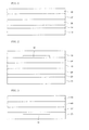
- FIGS 1 and 6 are sectional views showing a light emitting device and a method of manufacturing the same according to a first embodiment of the present invention
- FIG. 7 is a sectional view showing a light emitting device according to a second embodiment of the present invention.
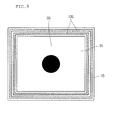
- FIG. 8 and 9 are a plan view showing the light emitting device according to the embodiments of the present invention.
- the light emitting device includes a second electrode layer 70, an ohmic contact layer 60 formed on the second electrode layer 70, a light emitting semiconductor layer including a second conductive semiconductor layer 50, an active layer 40, and a first conductive semiconductor layer 30 formed on the ohmic contact layer 60, and a first electrode layer 90 formed on the first conductive semiconductor layer 30.
- a reflective member 100 having an inclined surface is formed at a side of the light emitting semiconductor layer including the second conductive semiconductor layer 50, the active layer 40, and the first conductive semiconductor layer 30.
- the first conductive semiconductor layer 30 may include a nitride-based semiconductor layer having N-type impurities
- the second conductive semiconductor layer 50 may include a nitride-based semiconductor layer having P-type impurities.
- the active layer 40 may include a nitride-based semiconductor layer having a multiple quantum well structure such that electrons are combined with holes to produce light.
- the reflective member 100 may include a second conductive semiconductor, a stack structure of the second conductive semiconductor layer and the active layer, or a stack structure of the second conductive semiconductor layer, the active layer, and the first conductive semiconductor layer.
- the reflective member 100 may include a nitride-based semiconductor layer similarly to the light emitting semiconductor layer.
- the reflective member 100 is provided at the side of the light emitting semiconductor layer including the second conductive semiconductor layer 50, the active layer 40, and the first conductive semiconductor layer 30 while being spaced apart from the light emitting semiconductor layer. Accordingly, the reflective member 100 reflects light, which is emitted from the active layer 40 through a lateral side thereof, upwardly.
- light emitted from the light emitting device according to the present embodiment is forwarded upwardly, so that the light emitting efficiency of the light emitting device can be improved.
- FIG. 7 is a sectional view showing the light emitting device according to the second embodiment of the present invention.
- the light emitting device according to the second embodiment is similar to the light emitting device according to the first embodiment.
- a reflective layer 110 is formed at a lateral side of the reflective member 100.
- the reflective layer 110 may include gold (Ag) or aluminum (Al) representing superior reflectance.
- FIGS. 8 and 9 are plan views showing the light emitting device according to the embodiments.
- the reflective member 100 is formed at a side of the light emitting semiconductor layer including the second conductive semiconductor layer 50, the active layer 40, and the first conductive semiconductor layer 30 while being spaced apart from the light emitting semiconductor layer.
- the reflective member 100 may be provided in the form of a dot or a fence.
- the reflective member 100 may surround the light emitting semiconductor layer including the second conductive semiconductor layer 50, the active layer 40, and the first conductive semiconductor layer 30.
- the reflective member 100 may be provided in the combination form of the dot and the fence.
- the reflective member 100 may include one of fence type reflective members shown in FIG. 9 , and the dot type reflective member shown in FIG. 8 .
- an un-doped GaN layer 20, the first conductive semiconductor layer 30, the active layer 40, and the second conductive semiconductor layer 50 are formed on a substrate 10.
- a buffer layer (not shown) may be interposed between the substrate 10 and the un-doped GaN layer 20.
- the substrate 10 may include at least one of sapphire (Al 2 Os), silicon (Si), silicon carbide (SiC), gallium arsenide (GaAs), zinc oxide (ZnO), and magnesium oxide (MgO).
- sapphire Al 2 Os
- Si silicon
- SiC silicon carbide
- GaAs gallium arsenide
- ZnO zinc oxide
- MgO magnesium oxide
- the buffer layer may include a multi-layer having a stack structure such as AllnN/GaN, InxGa 1-x N/GaN, or Al x ln y Ga 1-x-y N/In x Ga 1-x N/GaN.
- the buffer layer may be grown by injecting trimethyl-gallium (TMGa), trimethyl-indium (TMIn) and trimethyl -aluminum (TMAI) into a chamber together with hydrogen gas and ammonia gas.
- the un-doped GaN layer 20 may be grown by injecting TMGa into the chamber together with hydrogen gas and the ammonia gas.
- the first conductive semiconductor layer 30 may include a nitride-based semiconductor layer implanted with first conductive impurity ions.
- the first conductive semiconductor layer 30 may be a semiconductor layer implanted with N-type impurity ions.
- the first conductive semiconductor layer 30 may be grown by injecting TMGa and silicon nitride (SiN 4 ) including N-type impurities (e.g., Si) into the chamber together with hydrogen gas and ammonia gas.
- the active layer 40 and the second conductive semiconductor layer 50 are formed on the first conductive layer 30.
- the active layer 40 may have a single quantum well structure or a multi-quantum well structure.
- the active layer 40 may include a stack structure of an InGaN well layer/a GaN barrier layer.
- the second conductive semiconductor layer 50 may include a nitride-based semiconductor layer implanted with second conductive impurity ions.
- the second conductive semiconductor layer 50 may include a semiconductor layer implanted with P-type impurity ions.
- the second conductive semiconductor layer 50 may be grown by injecting TMGa and bis-ethylcyclopentadienyl magnesium (EtCp 2 Mg) ⁇ Mg(C 2 HsCsH 4 ) 2 ⁇ including p type impurities (for example, Mg) into the chamber together with hydrogen gas and ammonia gas.
- the ohmic contact layer 60 and the second electrode layer 70 are formed on the second conductive semiconductor layer 50.
- the ohmic contact layer 60 may include a transparent electrode layer.
- the ohmic contact layer 60 may include at least one of ITO, ZnO, RuO x , TiO x , and IrO x .
- the ohmic contact layer 60 may include at least one of a reflective layer and an adhesive layer.
- the second electrode layer 70 may include at least one of titanium (Ti), chromium (Cr), nickel (Ni), aluminum (Al), platinum (Pt), gold (Au), and a conductive substrate.
- the substrate 10 and the un-doped GaN layer 20 are removed from the resultant structure of FIG. 2 . If the buffer layer has been formed, the buffer layer is removed.
- a mask 80 is formed on the first conductive semiconductor layer 30 in the resultant structure of FIG. 3 .
- the stack structure of the second conductive semiconductor layer 50, the active layer 40, and the first conductive semiconductor layer 30 is selectively etched through a dry etch process using the mask 80.
- the reflective member 100 is formed at the side of the light emitting semiconductor layer while being spaced apart from the light emitting semiconductor layer.
- the reflective member 100 may include a stack structure of the second conductive semiconductor layer, the active layer, and the first conductive semiconductor layer.
- the first electrode layer 90 is formed on the first conductive semiconductor layer 30.
- the reflective layer 110 may be formed on the surface of the reflective member 100. If the reflective layer 110 is additionally formed, the structure of FIG. 7 is obtained.
- any reference in this specification to "one embodiment,” “an embodiment,” “example embodiment,” etc. means that a particular feature, structure, or characteristic described in connection with the embodiment is included in at least one embodiment of the invention.
- the appearances of such phrases in various places in the specification are not necessarily all referring to the same embodiment.
- the embodiment can be adapted to a light emitting device used as a light source.
Landscapes
- Led Devices (AREA)
Abstract
Description
- The embodiment relates to a light emitting device.
- Recently, various studies and researches have been carried out regarding a device employing a light emitting diode (LED) as a light emitting device.
- The LED converts an electrical signal into light by using the characteristic of a compound semiconductor. The LED has the stack structure of a first conductive semiconductor layer, an active layer, and a second conductive semiconductor layer and emits light through the active layer as power is applied thereto. The first conductive semiconductor layer may serve as an N-type semiconductor layer, and the second conductive semiconductor layer may serve as a P-type semiconductor layer, or vice versa.
- Meanwhile, in such a light emitting device, the light emitted from the active layer is discharged through a lateral side as well as a top surface of the light emitting device, so that light emitting efficiency may be degraded.
- The embodiment provides a light emitting device having a novel structure and a method of manufacturing the same.
- The embodiment provides a light emitting device capable of improving light efficiency in the direction of a top surface thereof and a method of manufacturing the same.
- The embodiment provides a light emitting device capable of reflecting laterally emitted light in the direction of the top surface and a method of manufacturing the same.
- According to the embodiment, a light emitting device includes a second electrode layer, a light emitting semiconductor layer including a second conductive semiconductor layer, an active layer, and a first conductive semiconductor layer on the second electrode layer, a reflective member spaced apart from the light emitting semiconductor layer on the second electrode layer, and a first electrode layer on the first conductive semiconductor layer.
- According to the embodiment, the light emitting device includes a second electrode layer, a light emitting semiconductor layer including a second conductive semiconductor layer, an active layer, and a first conductive semiconductor layer on the second electrode layer, and a reflective member at an outside of the light emitting semiconductor layer.
- The embodiment can provide a light emitting device having a novel structure and a method of manufacturing the same.
- The embodiment can provide a light emitting device capable of improving light efficiency in the direction of a top surface thereof and a method of manufacturing the same.
- The embodiment can provide a light emitting device capable of reflecting light laterally emitted in the direction of a top surface and a method of manufacturing the same.
-
-
FIGS 1 and6 are sectional views showing a light emitting device and a method of manufacturing the same according to a first embodiment of the present invention; -
FIG. 7 is a sectional view showing a light emitting device according to a second embodiment of the present invention; -
FIG. 8 is a plan view showing the light emitting device according to the embodiments of the present invention; and -
FIG. 9 is a plan view showing the light emitting device according to the embodiments of the present invention. - In the description of the embodiments, it will be understood that, when a layer (or film), a region, a pattern, or a structure is referred to as being "on" or "under" another substrate, another layer (or film), another region, another pad, or another pattern, it can be "directly" or "indirectly" on the other substrate, layer (or film), region, pad, or pattern, or one or more intervening layers may also be present. Such a position of the layer has been described with reference to the drawings.
- The thickness and size of each layer shown in the drawings can be exaggerated, omitted or schematically drawn for the purpose of convenience or clarity. In addition, the size of elements does not utterly reflect an actual size.
-
FIGS 1 and6 are sectional views showing a light emitting device and a method of manufacturing the same according to a first embodiment of the present invention, andFIG. 7 is a sectional view showing a light emitting device according to a second embodiment of the present invention.FIG. 8 and9 are a plan view showing the light emitting device according to the embodiments of the present invention. - Referring to
FIG. 6 , the light emitting device according to the first embodiment of the present invention includes asecond electrode layer 70, anohmic contact layer 60 formed on thesecond electrode layer 70, a light emitting semiconductor layer including a secondconductive semiconductor layer 50, anactive layer 40, and a firstconductive semiconductor layer 30 formed on theohmic contact layer 60, and afirst electrode layer 90 formed on the firstconductive semiconductor layer 30. In addition, areflective member 100 having an inclined surface is formed at a side of the light emitting semiconductor layer including the secondconductive semiconductor layer 50, theactive layer 40, and the firstconductive semiconductor layer 30. - The first
conductive semiconductor layer 30 may include a nitride-based semiconductor layer having N-type impurities, and the secondconductive semiconductor layer 50 may include a nitride-based semiconductor layer having P-type impurities. Theactive layer 40 may include a nitride-based semiconductor layer having a multiple quantum well structure such that electrons are combined with holes to produce light. - The
reflective member 100 may include a second conductive semiconductor, a stack structure of the second conductive semiconductor layer and the active layer, or a stack structure of the second conductive semiconductor layer, the active layer, and the first conductive semiconductor layer. - In other words, the
reflective member 100 may include a nitride-based semiconductor layer similarly to the light emitting semiconductor layer. - The
reflective member 100 is provided at the side of the light emitting semiconductor layer including the secondconductive semiconductor layer 50, theactive layer 40, and the firstconductive semiconductor layer 30 while being spaced apart from the light emitting semiconductor layer. Accordingly, thereflective member 100 reflects light, which is emitted from theactive layer 40 through a lateral side thereof, upwardly. - Therefore, light emitted from the light emitting device according to the present embodiment is forwarded upwardly, so that the light emitting efficiency of the light emitting device can be improved.
-
FIG. 7 is a sectional view showing the light emitting device according to the second embodiment of the present invention. The light emitting device according to the second embodiment is similar to the light emitting device according to the first embodiment. - In order to improve the light emitting efficiency by the
reflective member 100, areflective layer 110 is formed at a lateral side of thereflective member 100. Thereflective layer 110 may include gold (Ag) or aluminum (Al) representing superior reflectance. -
FIGS. 8 and9 are plan views showing the light emitting device according to the embodiments. Thereflective member 100 is formed at a side of the light emitting semiconductor layer including the secondconductive semiconductor layer 50, theactive layer 40, and the firstconductive semiconductor layer 30 while being spaced apart from the light emitting semiconductor layer. Thereflective member 100 may be provided in the form of a dot or a fence. Thereflective member 100 may surround the light emitting semiconductor layer including the secondconductive semiconductor layer 50, theactive layer 40, and the firstconductive semiconductor layer 30. - In addition, the
reflective member 100 may be provided in the combination form of the dot and the fence. For example, thereflective member 100 may include one of fence type reflective members shown inFIG. 9 , and the dot type reflective member shown inFIG. 8 . - Hereinafter, the method of manufacturing the light emitting device according to the embodiment will be described in detail with reference to
FIGS. 1 to 6 . - Referring to
FIG. 1 , anun-doped GaN layer 20, the firstconductive semiconductor layer 30, theactive layer 40, and the secondconductive semiconductor layer 50 are formed on asubstrate 10. In addition, a buffer layer (not shown) may be interposed between thesubstrate 10 and theun-doped GaN layer 20. - The
substrate 10 may include at least one of sapphire (Al2Os), silicon (Si), silicon carbide (SiC), gallium arsenide (GaAs), zinc oxide (ZnO), and magnesium oxide (MgO). - The buffer layer may include a multi-layer having a stack structure such as AllnN/GaN, InxGa1-xN/GaN, or AlxlnyGa1-x-yN/InxGa1-xN/GaN. For example, the buffer layer may be grown by injecting trimethyl-gallium (TMGa), trimethyl-indium (TMIn) and trimethyl -aluminum (TMAI) into a chamber together with hydrogen gas and ammonia gas.
- The
un-doped GaN layer 20 may be grown by injecting TMGa into the chamber together with hydrogen gas and the ammonia gas. - The first
conductive semiconductor layer 30 may include a nitride-based semiconductor layer implanted with first conductive impurity ions. For example, the firstconductive semiconductor layer 30 may be a semiconductor layer implanted with N-type impurity ions. The firstconductive semiconductor layer 30 may be grown by injecting TMGa and silicon nitride (SiN4) including N-type impurities (e.g., Si) into the chamber together with hydrogen gas and ammonia gas. - Then, the
active layer 40 and the secondconductive semiconductor layer 50 are formed on the firstconductive layer 30. - The
active layer 40 may have a single quantum well structure or a multi-quantum well structure. For example, theactive layer 40 may include a stack structure of an InGaN well layer/a GaN barrier layer. - The second
conductive semiconductor layer 50 may include a nitride-based semiconductor layer implanted with second conductive impurity ions. For example, the secondconductive semiconductor layer 50 may include a semiconductor layer implanted with P-type impurity ions. The secondconductive semiconductor layer 50 may be grown by injecting TMGa and bis-ethylcyclopentadienyl magnesium (EtCp2Mg){Mg(C2HsCsH4)2} including p type impurities (for example, Mg) into the chamber together with hydrogen gas and ammonia gas. - Referring to
FIG. 2 , theohmic contact layer 60 and thesecond electrode layer 70 are formed on the secondconductive semiconductor layer 50. - The
ohmic contact layer 60 may include a transparent electrode layer. For example, theohmic contact layer 60 may include at least one of ITO, ZnO, RuOx, TiOx, and IrOx. - The
ohmic contact layer 60 may include at least one of a reflective layer and an adhesive layer. - The
second electrode layer 70 may include at least one of titanium (Ti), chromium (Cr), nickel (Ni), aluminum (Al), platinum (Pt), gold (Au), and a conductive substrate. - Referring to
FIG. 3 , thesubstrate 10 and theun-doped GaN layer 20 are removed from the resultant structure ofFIG. 2 . If the buffer layer has been formed, the buffer layer is removed. - Referring to
FIG. 4 , amask 80 is formed on the firstconductive semiconductor layer 30 in the resultant structure ofFIG. 3 . - The stack structure of the second
conductive semiconductor layer 50, theactive layer 40, and the firstconductive semiconductor layer 30 is selectively etched through a dry etch process using themask 80. - Referring to
FIG. 5 , after forming the light emitting semiconductor layer including the secondconductive semiconductor layer 50, theactive layer 40, and the firstconductive semiconductor layer 30 in order to emit light through the etch process ofFIG. 4 , thereflective member 100 is formed at the side of the light emitting semiconductor layer while being spaced apart from the light emitting semiconductor layer. - In this case, the
reflective member 100 may include a stack structure of the second conductive semiconductor layer, the active layer, and the first conductive semiconductor layer. - Referring to
FIG. 6 , thefirst electrode layer 90 is formed on the firstconductive semiconductor layer 30. - Meanwhile, as described above, the
reflective layer 110 may be formed on the surface of thereflective member 100. If thereflective layer 110 is additionally formed, the structure ofFIG. 7 is obtained. - Although embodiments have been described with reference to a number of illustrative embodiments thereof, it should be understood that numerous other modifications and embodiments can be devised by those skilled in the art that will fall within the spirit and scope of the principles of this disclosure. More particularly, various variations and modifications are possible in the component parts and/or arrangements of the subject combination arrangement within the scope of the disclosure, the drawings and the appended claims. In addition to variations and modifications in the component parts and/or arrangements, alternative uses will also be apparent to those skilled in the art.
- Any reference in this specification to "one embodiment," "an embodiment," "example embodiment," etc., means that a particular feature, structure, or characteristic described in connection with the embodiment is included in at least one embodiment of the invention. The appearances of such phrases in various places in the specification are not necessarily all referring to the same embodiment. Further, when a particular feature, structure, or characteristic is described in connection with any embodiment, it is submitted that it is within the purview of one skilled in the art to effect such feature, structure, or characteristic in connection with other ones of the embodiments.
- The embodiment can be adapted to a light emitting device used as a light source.
Claims (15)
- A light emitting device comprising:a second electrode layer;a light emitting semiconductor layer including a second conductive semiconductor layer, an active layer, and a first conductive semiconductor layer on the second electrode layer;a reflective member spaced apart from the light emitting semiconductor layer on the second electrode layer; anda first electrode layer on the first conductive semiconductor layer.
- The light emitting device of claim 1, further comprising a reflective layer on a surface of the reflective member.
- The light emitting device of claim 2, wherein the reflective layer includes gold (Ag) or aluminum (Al).
- The light emitting device of claim 1, wherein the reflective layer includes the second conductive semiconductor layer.
- The light emitting device of claim 1, wherein the reflective layer includes the second semiconductor layer and the active layer.
- The light emitting device of claim 1, wherein the reflective layer includes the second conductive semiconductor layer, an active layer, and the first conductive semiconductor layer.
- The light emitting device of claim 1, wherein the reflective member is provided at a side of the light emitting semiconductor layer and has a form of a plurality of dots.
- The light emitting device of claim 1, wherein the reflective member is provided at a side of the light emitting semiconductor layer and has a form of a fence.
- The light emitting device of claim 1, further comprising an ohmic contact layer interposed between the second electrode layer and the second conductive semiconductor layer.
- The light emitting device of claim 1, wherein the reflective member includes a nitride-based semiconductor layer.
- The light emitting device of claim 1, wherein a lateral side of the reflective member is an inclined surface.
- A light emitting device comprising:a second electrode layer;a light emitting semiconductor layer including a second conductive semiconductor layer, an active layer, and a first conductive semiconductor layer on the second electrode layer; anda reflective member at an outside of the light emitting semiconductor layer.
- The light emitting device of claim 12, further comprising a reflective layer on a surface of the reflective member.
- The light emitting device of claim 12, wherein the reflective member is provided on the second electrode layer, and includes the second conductive semiconductor layer, the active layer, and the first conductive semiconductor layer which are spaced apart from the light emitting semiconductor layer.
- The light emitting device of claim 12, wherein the reflective member is provided in a form of at least one of a fence and a plurality of dots.
Applications Claiming Priority (2)
| Application Number | Priority Date | Filing Date | Title |
|---|---|---|---|
| KR1020080042602A KR100952034B1 (en) | 2008-05-08 | 2008-05-08 | Light emitting device and manufacturing method |
| PCT/KR2009/002447 WO2009136769A2 (en) | 2008-05-08 | 2009-05-08 | Light-emitting element |
Publications (2)
| Publication Number | Publication Date |
|---|---|
| EP2280429A2 true EP2280429A2 (en) | 2011-02-02 |
| EP2280429A4 EP2280429A4 (en) | 2011-06-08 |
Family
ID=41265185
Family Applications (1)
| Application Number | Title | Priority Date | Filing Date |
|---|---|---|---|
| EP09742875A Ceased EP2280429A4 (en) | 2008-05-08 | 2009-05-08 | LUMINESCENT ELEMENT |
Country Status (6)
| Country | Link |
|---|---|
| US (2) | US8013353B2 (en) |
| EP (1) | EP2280429A4 (en) |
| JP (1) | JP4824129B2 (en) |
| KR (1) | KR100952034B1 (en) |
| CN (2) | CN102646771B (en) |
| WO (1) | WO2009136769A2 (en) |
Families Citing this family (6)
| Publication number | Priority date | Publication date | Assignee | Title |
|---|---|---|---|---|
| KR100999787B1 (en) | 2009-12-29 | 2010-12-08 | 엘지이노텍 주식회사 | Light emitting device, manufacturing method and light emitting device package |
| CN102339923A (en) * | 2010-07-28 | 2012-02-01 | 展晶科技(深圳)有限公司 | LED chip |
| KR102070092B1 (en) | 2014-01-09 | 2020-01-29 | 삼성전자주식회사 | Semiconductor light emitting device |
| CN104821354A (en) * | 2015-05-07 | 2015-08-05 | 合肥彩虹蓝光科技有限公司 | Method for reducing light emitting angle of LED chip |
| EP3342795B1 (en) | 2015-08-24 | 2023-01-04 | 3-D Matrix, Ltd. | Biodegradable injectable gel |
| CN114628560A (en) * | 2022-03-21 | 2022-06-14 | 聚灿光电科技(宿迁)有限公司 | An enhanced LED structure |
Family Cites Families (17)
| Publication number | Priority date | Publication date | Assignee | Title |
|---|---|---|---|---|
| JPS5896781A (en) * | 1981-12-03 | 1983-06-08 | Matsushita Electric Ind Co Ltd | Method for manufacturing semiconductor light emitting device |
| JPS6276686A (en) * | 1985-09-30 | 1987-04-08 | Toshiba Corp | Light emitting element |
| JP3537881B2 (en) * | 1994-03-29 | 2004-06-14 | 株式会社リコー | LED array head |
| US6633120B2 (en) * | 1998-11-19 | 2003-10-14 | Unisplay S.A. | LED lamps |
| JP2002280602A (en) | 2001-03-21 | 2002-09-27 | Toshiba Corp | Vertical cavity type light emitting diode and optical transmission module using the light emitting diode |
| JP3896044B2 (en) | 2002-07-11 | 2007-03-22 | シャープ株式会社 | Nitride-based semiconductor light-emitting device manufacturing method and product |
| JP4147073B2 (en) * | 2002-09-02 | 2008-09-10 | シャープ株式会社 | Manufacturing method of light emitting diode |
| JP2004128321A (en) | 2002-10-04 | 2004-04-22 | Matsushita Electric Works Ltd | Semiconductor light emitting device |
| US20060034084A1 (en) * | 2004-06-28 | 2006-02-16 | Kyocera Corporation | Light-emitting apparatus and illuminating apparatus |
| KR100568830B1 (en) * | 2004-08-26 | 2006-04-10 | 에피밸리 주식회사 | III-nitride semiconductor light emitting device |
| CN100403562C (en) * | 2005-03-15 | 2008-07-16 | 金芃 | Vertically structured semiconductor chips or devices |
| JP2006332225A (en) * | 2005-05-25 | 2006-12-07 | Sony Corp | Nitride-based light emitting diode |
| JP2007103725A (en) | 2005-10-05 | 2007-04-19 | Toshiba Corp | Semiconductor light emitting device |
| KR100756842B1 (en) * | 2006-03-14 | 2007-09-07 | 서울옵토디바이스주식회사 | Light-emitting diode having light extraction columns and method of manufacturing same |
| JP5082504B2 (en) | 2006-03-31 | 2012-11-28 | 日亜化学工業株式会社 | Light emitting device and method for manufacturing light emitting device |
| CN101055906A (en) * | 2006-04-11 | 2007-10-17 | 汉光科技股份有限公司 | High brightness light emitting diode and its manufacturing method |
| KR100781660B1 (en) * | 2006-05-18 | 2007-12-05 | 서울옵토디바이스주식회사 | Light emitting device having light emitting band and manufacturing method thereof |
-
2008
- 2008-05-08 KR KR1020080042602A patent/KR100952034B1/en active Active
-
2009
- 2009-05-08 JP JP2010549587A patent/JP4824129B2/en active Active
- 2009-05-08 CN CN201210111384.5A patent/CN102646771B/en not_active Expired - Fee Related
- 2009-05-08 EP EP09742875A patent/EP2280429A4/en not_active Ceased
- 2009-05-08 CN CN2009801009941A patent/CN101861662B/en active Active
- 2009-05-08 WO PCT/KR2009/002447 patent/WO2009136769A2/en not_active Ceased
- 2009-05-08 US US12/812,403 patent/US8013353B2/en active Active
-
2011
- 2011-07-21 US US13/188,275 patent/US8395174B2/en active Active
Also Published As
| Publication number | Publication date |
|---|---|
| CN102646771A (en) | 2012-08-22 |
| WO2009136769A2 (en) | 2009-11-12 |
| KR100952034B1 (en) | 2010-04-07 |
| US20110278625A1 (en) | 2011-11-17 |
| KR20090116841A (en) | 2009-11-12 |
| US20100289050A1 (en) | 2010-11-18 |
| CN101861662B (en) | 2012-06-13 |
| CN102646771B (en) | 2016-01-20 |
| EP2280429A4 (en) | 2011-06-08 |
| CN101861662A (en) | 2010-10-13 |
| US8395174B2 (en) | 2013-03-12 |
| JP2011513985A (en) | 2011-04-28 |
| US8013353B2 (en) | 2011-09-06 |
| JP4824129B2 (en) | 2011-11-30 |
| WO2009136769A3 (en) | 2010-03-11 |
Similar Documents
| Publication | Publication Date | Title |
|---|---|---|
| EP2270881B1 (en) | Light-emitting element and a production method therefor | |
| KR101449030B1 (en) | group 3 nitride-based semiconductor light emitting diodes and methods to fabricate them | |
| CN101740695B (en) | Light emitting device and method for manufacturing the same | |
| US10121939B2 (en) | Semiconductor light-emitting devices and methods of manufacturing the same | |
| KR100986461B1 (en) | Light emitting device and manufacturing method | |
| KR101047718B1 (en) | Light emitting element | |
| JP2009502043A (en) | Blue light-emitting diode with uneven high refractive index surface for improved light extraction efficiency | |
| KR20090106299A (en) | Group III-nitride semiconductor light emitting diode device having an ohmic contact light extracting structure layer and a method of manufacturing the same | |
| US9231165B2 (en) | Light-emitting diode chip | |
| KR20110072424A (en) | Light emitting device, light emitting device package and manufacturing method | |
| US8395174B2 (en) | Light-emitting element | |
| US20180019378A1 (en) | Method For Fabricating High-Efficiency Light Emitting Diode Having Light Emitting Window Electrode Structure | |
| US20050224990A1 (en) | High reflectivity p-contacts for group III-nitride light emitting diodes | |
| CN101478021B (en) | Group III Nitride Semiconductor Light-Emitting Devices | |
| CN102132427B (en) | Light emitting device and manufacturing method thereof | |
| KR20120055332A (en) | Light emitting device and light emitting device package | |
| KR101124470B1 (en) | Semiconductor light emitting device | |
| KR101084641B1 (en) | Group III nitride semiconductor light emitting device | |
| KR20090116842A (en) | Light emitting device and manufacturing method | |
| US20140054544A1 (en) | Light emitting device | |
| JP2006173533A (en) | Light emitting device |
Legal Events
| Date | Code | Title | Description |
|---|---|---|---|
| PUAI | Public reference made under article 153(3) epc to a published international application that has entered the european phase |
Free format text: ORIGINAL CODE: 0009012 |
|
| 17P | Request for examination filed |
Effective date: 20100611 |
|
| AK | Designated contracting states |
Kind code of ref document: A2 Designated state(s): AT BE BG CH CY CZ DE DK EE ES FI FR GB GR HR HU IE IS IT LI LT LU LV MC MK MT NL NO PL PT RO SE SI SK TR |
|
| AX | Request for extension of the european patent |
Extension state: AL BA RS |
|
| A4 | Supplementary search report drawn up and despatched |
Effective date: 20110506 |
|
| DAX | Request for extension of the european patent (deleted) | ||
| 17Q | First examination report despatched |
Effective date: 20130109 |
|
| RAP1 | Party data changed (applicant data changed or rights of an application transferred) |
Owner name: LG INNOTEK CO., LTD. |
|
| REG | Reference to a national code |
Ref country code: DE Ref legal event code: R003 |
|
| STAA | Information on the status of an ep patent application or granted ep patent |
Free format text: STATUS: THE APPLICATION HAS BEEN REFUSED |
|
| 18R | Application refused |
Effective date: 20160303 |