EP2278596A2 - Procédé de fabrication et de commande d'un composant de résistance réglable et son utilisation - Google Patents
Procédé de fabrication et de commande d'un composant de résistance réglable et son utilisation Download PDFInfo
- Publication number
- EP2278596A2 EP2278596A2 EP10006266A EP10006266A EP2278596A2 EP 2278596 A2 EP2278596 A2 EP 2278596A2 EP 10006266 A EP10006266 A EP 10006266A EP 10006266 A EP10006266 A EP 10006266A EP 2278596 A2 EP2278596 A2 EP 2278596A2
- Authority
- EP
- European Patent Office
- Prior art keywords
- actuator
- base body
- resistance
- resistor
- power semiconductor
- Prior art date
- Legal status (The legal status is an assumption and is not a legal conclusion. Google has not performed a legal analysis and makes no representation as to the accuracy of the status listed.)
- Withdrawn
Links
- 238000004519 manufacturing process Methods 0.000 title claims description 4
- 239000004065 semiconductor Substances 0.000 claims abstract description 32
- 238000000034 method Methods 0.000 claims abstract description 10
- 239000000463 material Substances 0.000 claims abstract description 5
- 230000000694 effects Effects 0.000 claims description 4
- 239000000853 adhesive Substances 0.000 claims description 2
- 230000001070 adhesive effect Effects 0.000 claims description 2
- 229910000679 solder Inorganic materials 0.000 claims description 2
- 230000009471 action Effects 0.000 description 6
- 230000008859 change Effects 0.000 description 6
- XUIMIQQOPSSXEZ-UHFFFAOYSA-N Silicon Chemical compound [Si] XUIMIQQOPSSXEZ-UHFFFAOYSA-N 0.000 description 4
- 229910052710 silicon Inorganic materials 0.000 description 4
- 239000010703 silicon Substances 0.000 description 4
- 230000008901 benefit Effects 0.000 description 3
- 239000002800 charge carrier Substances 0.000 description 3
- 150000001875 compounds Chemical class 0.000 description 3
- 239000013078 crystal Substances 0.000 description 3
- XLOMVQKBTHCTTD-UHFFFAOYSA-N Zinc monoxide Chemical compound [Zn]=O XLOMVQKBTHCTTD-UHFFFAOYSA-N 0.000 description 2
- 238000009413 insulation Methods 0.000 description 2
- 230000004048 modification Effects 0.000 description 2
- 238000012986 modification Methods 0.000 description 2
- 230000015572 biosynthetic process Effects 0.000 description 1
- 230000006835 compression Effects 0.000 description 1
- 238000007906 compression Methods 0.000 description 1
- 230000001276 controlling effect Effects 0.000 description 1
- 230000001419 dependent effect Effects 0.000 description 1
- 238000007599 discharging Methods 0.000 description 1
- 230000008569 process Effects 0.000 description 1
- 230000001105 regulatory effect Effects 0.000 description 1
- 239000011787 zinc oxide Substances 0.000 description 1
Images


Classifications
-
- H—ELECTRICITY
- H01—ELECTRIC ELEMENTS
- H01C—RESISTORS
- H01C10/00—Adjustable resistors
- H01C10/10—Adjustable resistors adjustable by mechanical pressure or force
- H01C10/103—Adjustable resistors adjustable by mechanical pressure or force by using means responding to magnetic or electric fields, e.g. by addition of magnetisable or piezoelectric particles to the resistive material, or by an electromagnetic actuator
-
- H—ELECTRICITY
- H10—SEMICONDUCTOR DEVICES; ELECTRIC SOLID-STATE DEVICES NOT OTHERWISE PROVIDED FOR
- H10D—INORGANIC ELECTRIC SEMICONDUCTOR DEVICES
- H10D48/00—Individual devices not covered by groups H10D1/00 - H10D44/00
- H10D48/50—Devices controlled by mechanical forces, e.g. pressure
-
- H—ELECTRICITY
- H10—SEMICONDUCTOR DEVICES; ELECTRIC SOLID-STATE DEVICES NOT OTHERWISE PROVIDED FOR
- H10N—ELECTRIC SOLID-STATE DEVICES NOT OTHERWISE PROVIDED FOR
- H10N30/00—Piezoelectric or electrostrictive devices
- H10N30/20—Piezoelectric or electrostrictive devices with electrical input and mechanical output, e.g. functioning as actuators or vibrators
- H10N30/202—Piezoelectric or electrostrictive devices with electrical input and mechanical output, e.g. functioning as actuators or vibrators using longitudinal or thickness displacement combined with bending, shear or torsion displacement
Definitions
- the invention describes a method for the production and operation of a controllable resistance component whose resistance value changes during operation by an electrical manipulated variable can be regulated.
- the speed of this control should be at least in the range of a few kilohertz, since a significant use of this variable resistance device is in the control of power semiconductor switches.
- Such power semiconductor switches as they are used in a variety of power electronic circuits are often switched by charging or discharging a control terminal (gate).
- Current applications of such power semiconductor switches have a sequence of drive signals in the range of more than one kilohertz in the context of pulse wave modulation methods.
- Circuit arrangements with a driver circuit and at least one power semiconductor switch are generally known, wherein two current paths are provided between the driver circuit and the control terminal of the respective power semiconductor switch, each with a resistor for the on and off pulse. This is preferred because the requirements for the voltage and current characteristics at power-up differ from those at power-off.
- the present invention is based on the object of providing a method for producing and controlling a controllable resistance component which has switching or control speeds in the range of more than one kilohertz and which is used in a circuit arrangement for driving a power semiconductor switch.
- the basis of the controllable resistance component produced according to the invention is a resistance base made of a semiconductor material, preferably p-doped silicon. Furthermore, it is particularly preferred if the resistor base body consists of a layer arrangement of a first partial body of low doping and a second partial body of higher doping. With a suitable choice of the doping, the second partial body then has a resistance value which is at least three orders of magnitude less than that of the first partial body. Thus contributes to the effective power line in the resistance base significantly only the second body part.
- the resistance of semiconductor material depends on the charge carrier mobility.
- An influencing factor for this charge carrier mobility is the effect of tension or pressure in a suitable direction of the crystal lattice.
- suitable p-doped silicon it is possible to increase the charge carrier mobility of the holes by approximately one factor when exposed to ⁇ 100> or ⁇ 110> orientation of the crystal lattice and a compression or expansion of 1% of the expansion. It has proved to be advantageous for this purpose to provide the doping concentration of the first partial body with approximately 1x10 12 cm -3 , while the doping concentration of the second partial body with approximately 1x10 19 cm -3 is provided.
- At least one electrically controllable actuator is provided according to the invention, which preferably provides the inverse piezoelectric effect for carrying out the movement.
- Such actuators are basically known in the form of different crystals.
- the actuator for introducing a force to the resistor base body is materially arranged with a connection surface which is at least partially parallel to a first main surface of the resistor body.
- a mechanical force can act on this resistor base body and change its resistance value.
- the resistance base body preferably the second part body, first contact surfaces to form an electrical connection.
- the actuator has second contact surface to its electrical connection.
- the actuator By applying a suitable voltage, preferably of the order of 10V, the actuator expands or contracts, with a mechanical force being introduced with a main direction parallel or perpendicular to its first main surface, depending on its arrangement relative to the resistor base. In a main direction of action perpendicular to the first main surface, it is preferred if the actuator can be supported for introducing force against an abutment.
- a housing to the controllable resistance offers.
- This main direction of action of the mechanical force perpendicular to the first main surface of the resistor base body has the advantage, particularly in the embodiment as a layer sequence comprising a first and a second partial body, that the mechanical force acts uniformly on the volume of the second partial body that is covered by the actuator for the power line.
- a main direction of the mechanical force parallel to the first main surface of the main body of resistance has the significant advantage that an abutment in the above-mentioned sense can be dispensed with.
- the mechanical force does not act evenly on the volume covered by the actuator.
- the resistance base body forms a trough whose surface serves at least partially as a connection surface with the actuator, wherein the actuator is at least partially disposed in this trough.
- the inventively produced and controlled variable resistance device according to the invention is used in the control of a power semiconductor switch.
- the circuit arrangement here has a driver circuit whose control output is connected to the control input of the power semiconductor switch via the controllable resistance component.
- the driver circuit For switching on and off of the power semiconductor switch, the driver circuit applies a control signal via the controllable resistor to the control input of the power semiconductor switch. At least in one of the two switching operations, the driver circuit controls the resistance of the variable-resistance device so as to adjust the desired current and voltage during the switching process.
- the drive signal for switching on the power semiconductor switch may be set a first constant resistance value at the controllable resistor and for the drive signal for switching off the power semiconductor switch to set a second constant resistance value at the controllable resistor.
- these two resistance values differ by at least a factor of 2.
- a further preferred embodiment of the use for driving a power semiconductor switch at least for one of the drive signals for switching on or off of the power semiconductor switch during the duration of the respective drive signal variable resistance to the variable resistor, which is controlled by the driver circuit accordingly.
- this resistance value can be selected in the simplest case depending on the current voltage of the drive signal.
- the invention is based on embodiments in conjunction with the Fig. 1 to 3 explained in more detail.
- Fig. 1 shows a first embodiment of a variable resistance device according to the invention produced.
- Fig. 2 shows a second embodiment of a variable resistance device according to the invention produced.
- Fig. 3 shows a modification of the second embodiment.
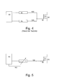
- Fig. 4 shows a circuit arrangement according to the prior art for driving a power semiconductor switch.
- Fig. 5 shows a circuit arrangement for driving according to the invention of a power semiconductor switch.
- Fig. 1 shows an inventively manufactured controllable resistance device (1). Shown is the cuboid resistance base body (10) with a typical length extension (x-direction) of 6mm of a width (z-direction) of 2mm and a height (y-direction) of 500 ⁇ m. This is formed as a planar layer arrangement of a first (12) and a second (14) part body.
- the first partial body (12) has a height of 499.8 ⁇ m and a p-type doping of 1 ⁇ 10 12 cm -3
- the second partial body (14) has a height of 200 nm and a p-type doping of 1 ⁇ 10 19 cm -3 ,
- the first partial body (12) does not contribute significantly to the electrical longitudinal conduction, since it has a resistance value of the order of magnitude of 1 MOhm, while the second partial body (14) has a resistance value of the order of magnitude of 100hm. Therefore, the first contact surfaces (20 a / b) for the electrical connection of the resistor base body (10) on the first second main body (14) associated first main surface (18 a) are provided.
- the actuator (30) a piezoelectric element
- the piezobau element (30) is arranged on the first surface (16) and by an insulating layer (22) of this electrically isolated.
- the insulation layer (22) is a permanent cohesive connection advantageous because it mechanically force on the resistance base body (10) is initiated.
- cohesive compounds sintered compounds have proven particularly useful, but there are also adhesive or solder joints used. Due to layer growth, it may be particularly preferable to allow the piezo component (30) to grow directly on the silicon body of the resistor base body (10). Such compounds have a particularly long life. It may further be preferred to form the piezobauelement (30) by juxtaposition of individual components, since this increases the working stroke.
- the term "working stroke” should be understood to mean the maximum relative change in length of the piezo component (30).
- the piezo component (30) has its own second contact surfaces (32 a / b) for its electrical control, whereby the controllable resistance component (1) forms a 4-pole.
- the controllable resistance component (1) forms a 3-pole and in this case one of the two second contact surfaces (32 a / b) has an electrical connection to the resistor base body (10), here in particular the second partial body (14). , having.
- a change in the resistance value is now achieved by a voltage is applied to the piezo components (30) and thereby mechanical force on the resistor base body (10), in particular on the second part body (14), is initiated.
- Essential here is the arrangement of the piezobau element (30) from which its main direction of action depends.
- main direction of action is here understood that dimension in the x or y direction, which has the largest working stroke.
- Fig. 2 shows a second embodiment of a variable resistance element (1) produced according to the invention.
- the basic elements of this embodiment are identical to those of the first embodiment.
- the resistance base body (10) here has a trough (140) whose surface partially forms the contact surface (16) with the piezo component (30) and here advantageously also has an insulation layer (22).
- the piezobau element (30) is in this case at least partially, but advantageously completely arranged in this trough (140) of the resistor main body (10), wherein a contact with all partial surfaces of the trough (140) is not necessary.
- the essential advantage of this embodiment is that the mechanical force with a main direction of action parallel (34) to the first major surface (18a) perpendicular to the corresponding portion of the second part body (14) acts without an additional abutment is necessary.
- Fig. 3 shows a modification of the second embodiment.
- the first (12) and second partial body (14) of the resistor base body (10) are formed such that a trough (140) forms and from this starting a channel (142) of higher doping to the second main surface (18b) of the main body resistance (10th ) is provided.
- One of the two first contact surfaces (20a) may here be formed circumferentially around this trough (140), while the other first contact surface (20b) is advantageously arranged on the opposite second main surface (18b) such that it covers at least approximately the entire second main surface (20b). 18b).
- the control range of the resistance component (1) is widened and / or improved in its meterability.
- Fig. 4 shows a circuit arrangement according to the prior art for driving a power semiconductor switch (60). Shown is a driver circuit (50) and a first (520) and second (540) current path to the control terminal (62) of a power semiconductor switch (60), for example an IGBT or a MOS-FET.
- a first resistor (52) having a first resistance value is arranged in the first current path (520), while analogously in the second current current (540) a second resistor (54) having a second resistance value is arranged to that of the turn-off signal.
- the two resistance values of the first (52) and second (54) resistances differ by at least a factor of 2 and are on the order of 100hm for driving individual power semiconductor switches (60).
- Fig. 5 shows a circuit arrangement for driving according to the invention of a power semiconductor switch (60). This differs from the prior art according to Fig. 2 by only one current path (100) from the driver circuit (50) to the power semiconductor switch (60). The resistance in this current path is a variable resistance device (1), as shown in Fig. 1 described. Furthermore, the circuit arrangement has a control path (102) from the driver circuit (50) to the controllable resistance component (1) in order to be able to regulate its resistance value.
- the control in one of the two switching states, the switching on or off of the power semiconductor switch (60), the control will not intervene and the basic value of the controllable resistance component (1) of exemplary 40V will remain unchanged.
- the resistance value is reduced to 10V by applying a voltage in the range of 10V to the variable resistor (1) whose resistance value is lowered.
- the high control speed due to the piezo component (30) also permits a change in the resistance value during the duration of a control signal, the change in the resistance value of the controllable resistance component (1).
- a much more flexible control of the power semiconductor switch (60) is possible compared to the prior art.
Landscapes
- Physics & Mathematics (AREA)
- Electromagnetism (AREA)
- Engineering & Computer Science (AREA)
- Microelectronics & Electronic Packaging (AREA)
- Micromachines (AREA)
- Adjustable Resistors (AREA)
- Electronic Switches (AREA)
Applications Claiming Priority (1)
| Application Number | Priority Date | Filing Date | Title |
|---|---|---|---|
| DE102009034777.1A DE102009034777B4 (de) | 2009-07-25 | 2009-07-25 | Verfahren zu Herstellung eines regelbaren Widerstandsbauelements und dessen Verwendung |
Publications (2)
| Publication Number | Publication Date |
|---|---|
| EP2278596A2 true EP2278596A2 (fr) | 2011-01-26 |
| EP2278596A3 EP2278596A3 (fr) | 2015-07-08 |
Family
ID=43033527
Family Applications (1)
| Application Number | Title | Priority Date | Filing Date |
|---|---|---|---|
| EP10006266.0A Withdrawn EP2278596A3 (fr) | 2009-07-25 | 2010-06-17 | Procédé de fabrication et de commande d'un composant de résistance réglable et son utilisation |
Country Status (2)
| Country | Link |
|---|---|
| EP (1) | EP2278596A3 (fr) |
| DE (1) | DE102009034777B4 (fr) |
Family Cites Families (7)
| Publication number | Priority date | Publication date | Assignee | Title |
|---|---|---|---|---|
| US3138726A (en) * | 1960-11-17 | 1964-06-23 | Gulton Ind Inc | Transducer |
| DE69512544T2 (de) * | 1994-03-18 | 2000-05-25 | The Foxboro Co., Foxboro | Halbleiter-Druckwandler mit Einkristall-Silizium-Membran und Einkristall-Dehnungsmessstreifen und Herstellungsverfahren dazu |
| DE19747566C1 (de) * | 1997-10-28 | 1999-04-08 | Fraunhofer Ges Forschung | Piezoangetriebenes Spannungswellen-Getriebe |
| JP4630733B2 (ja) * | 2005-05-31 | 2011-02-09 | 株式会社東芝 | 半導体装置 |
| DE102005045099B4 (de) * | 2005-09-21 | 2011-05-05 | Infineon Technologies Ag | Entsättigungsschaltung mit einem IGBT |
| FR2916305B1 (fr) * | 2007-05-15 | 2009-10-23 | Commissariat Energie Atomique | Dispositif a transistor a canal contraint. |
| DE102008008931B3 (de) * | 2008-02-13 | 2009-07-16 | Fraunhofer-Gesellschaft zur Förderung der angewandten Forschung e.V. | Vorrichtung und Verfahren zum Schalten von elektrischen Signalen und Leistungen |
-
2009
- 2009-07-25 DE DE102009034777.1A patent/DE102009034777B4/de not_active Expired - Fee Related
-
2010
- 2010-06-17 EP EP10006266.0A patent/EP2278596A3/fr not_active Withdrawn
Non-Patent Citations (1)
| Title |
|---|
| None |
Also Published As
| Publication number | Publication date |
|---|---|
| EP2278596A3 (fr) | 2015-07-08 |
| DE102009034777A1 (de) | 2011-01-27 |
| DE102009034777B4 (de) | 2015-12-10 |
Similar Documents
| Publication | Publication Date | Title |
|---|---|---|
| DE1514362B1 (de) | Feldeffekttransistor | |
| DE102008030248A1 (de) | Ansteuerschaltung sowie Verfahren zur Ansteuerung von Piezoeinheit, insbesondere trimorphem Piezoaktor | |
| DE69921607T2 (de) | Verfahren zum Entfernen von Kurzschluss-Abschnitten einer Solarzelle | |
| DE102008057066A1 (de) | Wieder konfigurierbare Halbleitervorrichtung | |
| WO2018095921A1 (fr) | Circuit d'attaque, en particulier pour une cellule de pockels, et procédé permettant de faire fonctionner un circuit d'attaque | |
| DE112023003227T5 (de) | Integrierter pcm-treiber | |
| DE2153284A1 (de) | Speichermatrix | |
| DE102009027340A1 (de) | Ansteuerschaltung für mehrere induktive Lasten | |
| DE102005018344A1 (de) | Schaltvorrichtung für rekonfigurierbare Zwischenverbindung und Verfahren zum Herstellen derselben | |
| DE102009034777B4 (de) | Verfahren zu Herstellung eines regelbaren Widerstandsbauelements und dessen Verwendung | |
| DE102016107931A1 (de) | Elektronisches Bauelement zur Einschaltstrombegrenzung und Verwendung eines elektronischen Bauelements | |
| DE2158270C3 (de) | Kontaktloser Schalter mit einem Feldeffekt-Thyristor | |
| DE1212221B (de) | Halbleiterbauelement mit einem scheibenfoermigen Halbleiterkoerper und zwei sperrfreien Basiselektroden | |
| DE19527486A1 (de) | MOS-Transistor für hohe Leistung | |
| WO2009153266A1 (fr) | Composant piézoélectrique et procédé de fabrication d'un contact électrique | |
| EP1595294A1 (fr) | Procede de production d'un contact electrique d'un actionneur piezo-electrique et polarisation de l'actionneur piezo-electrique | |
| WO2014086611A1 (fr) | Procédé de fabrication d'un composant électronique | |
| DE102022116270A1 (de) | Ansteuerungsvorrichtung | |
| DE2637481A1 (de) | Duennschicht-transistoreinrichtung | |
| DE102019123883B4 (de) | Dielektrische Elastomer Vorrichtung als EMV optimiertes Stapelsystem | |
| DE102007049769A1 (de) | Feldeffekttransistor mit gekröpftem Mehrfach-Gate-Aufbau | |
| DE2150311A1 (de) | Temperaturabhaengiger elektrischer schalter mit einem bimetallischen steuerorgan | |
| EP1526623A1 (fr) | Circuit de limitation d'un courant d'appel | |
| DE2555881C3 (de) | Ladungsgekoppeltes Halbleiterbauelement | |
| DE2538361C3 (de) | Multistabile Speicherschaltung, die zwei zusammengeschaltete MNOS-Feldeffekttransistoren enthält |
Legal Events
| Date | Code | Title | Description |
|---|---|---|---|
| PUAI | Public reference made under article 153(3) epc to a published international application that has entered the european phase |
Free format text: ORIGINAL CODE: 0009012 |
|
| AK | Designated contracting states |
Kind code of ref document: A2 Designated state(s): AL AT BE BG CH CY CZ DE DK EE ES FI FR GB GR HR HU IE IS IT LI LT LU LV MC MK MT NL NO PL PT RO SE SI SK SM TR |
|
| AX | Request for extension of the european patent |
Extension state: BA ME RS |
|
| PUAL | Search report despatched |
Free format text: ORIGINAL CODE: 0009013 |
|
| AK | Designated contracting states |
Kind code of ref document: A3 Designated state(s): AL AT BE BG CH CY CZ DE DK EE ES FI FR GB GR HR HU IE IS IT LI LT LU LV MC MK MT NL NO PL PT RO SE SI SK SM TR |
|
| AX | Request for extension of the european patent |
Extension state: BA ME RS |
|
| RIC1 | Information provided on ipc code assigned before grant |
Ipc: H01L 29/84 20060101ALI20150603BHEP Ipc: H01L 29/78 20060101ALI20150603BHEP Ipc: H01C 10/10 20060101AFI20150603BHEP |
|
| STAA | Information on the status of an ep patent application or granted ep patent |
Free format text: STATUS: THE APPLICATION HAS BEEN WITHDRAWN |
|
| 18W | Application withdrawn |
Effective date: 20151016 |