EP2277192B1 - Solarzellen und herstellungsverfahren für solarzellen - Google Patents
Solarzellen und herstellungsverfahren für solarzellen Download PDFInfo
- Publication number
- EP2277192B1 EP2277192B1 EP09747280.7A EP09747280A EP2277192B1 EP 2277192 B1 EP2277192 B1 EP 2277192B1 EP 09747280 A EP09747280 A EP 09747280A EP 2277192 B1 EP2277192 B1 EP 2277192B1
- Authority
- EP
- European Patent Office
- Prior art keywords
- junction
- layer
- photovoltaic cell
- junctions
- absorber layer
- Prior art date
- Legal status (The legal status is an assumption and is not a legal conclusion. Google has not performed a legal analysis and makes no representation as to the accuracy of the status listed.)
- Not-in-force
Links
Images


Classifications
-
- H—ELECTRICITY
- H10—SEMICONDUCTOR DEVICES; ELECTRIC SOLID-STATE DEVICES NOT OTHERWISE PROVIDED FOR
- H10F—INORGANIC SEMICONDUCTOR DEVICES SENSITIVE TO INFRARED RADIATION, LIGHT, ELECTROMAGNETIC RADIATION OF SHORTER WAVELENGTH OR CORPUSCULAR RADIATION
- H10F77/00—Constructional details of devices covered by this subclass
- H10F77/10—Semiconductor bodies
- H10F77/14—Shape of semiconductor bodies; Shapes, relative sizes or dispositions of semiconductor regions within semiconductor bodies
- H10F77/146—Superlattices; Multiple quantum well structures
-
- B—PERFORMING OPERATIONS; TRANSPORTING
- B82—NANOTECHNOLOGY
- B82Y—SPECIFIC USES OR APPLICATIONS OF NANOSTRUCTURES; MEASUREMENT OR ANALYSIS OF NANOSTRUCTURES; MANUFACTURE OR TREATMENT OF NANOSTRUCTURES
- B82Y20/00—Nanooptics, e.g. quantum optics or photonic crystals
-
- H—ELECTRICITY
- H10—SEMICONDUCTOR DEVICES; ELECTRIC SOLID-STATE DEVICES NOT OTHERWISE PROVIDED FOR
- H10F—INORGANIC SEMICONDUCTOR DEVICES SENSITIVE TO INFRARED RADIATION, LIGHT, ELECTROMAGNETIC RADIATION OF SHORTER WAVELENGTH OR CORPUSCULAR RADIATION
- H10F10/00—Individual photovoltaic cells, e.g. solar cells
- H10F10/10—Individual photovoltaic cells, e.g. solar cells having potential barriers
- H10F10/16—Photovoltaic cells having only PN heterojunction potential barriers
- H10F10/161—Photovoltaic cells having only PN heterojunction potential barriers comprising multiple PN heterojunctions, e.g. tandem cells
-
- H—ELECTRICITY
- H10—SEMICONDUCTOR DEVICES; ELECTRIC SOLID-STATE DEVICES NOT OTHERWISE PROVIDED FOR
- H10F—INORGANIC SEMICONDUCTOR DEVICES SENSITIVE TO INFRARED RADIATION, LIGHT, ELECTROMAGNETIC RADIATION OF SHORTER WAVELENGTH OR CORPUSCULAR RADIATION
- H10F10/00—Individual photovoltaic cells, e.g. solar cells
- H10F10/10—Individual photovoltaic cells, e.g. solar cells having potential barriers
- H10F10/16—Photovoltaic cells having only PN heterojunction potential barriers
- H10F10/162—Photovoltaic cells having only PN heterojunction potential barriers comprising only Group II-VI materials, e.g. CdS/CdTe photovoltaic cells
-
- H—ELECTRICITY
- H10—SEMICONDUCTOR DEVICES; ELECTRIC SOLID-STATE DEVICES NOT OTHERWISE PROVIDED FOR
- H10F—INORGANIC SEMICONDUCTOR DEVICES SENSITIVE TO INFRARED RADIATION, LIGHT, ELECTROMAGNETIC RADIATION OF SHORTER WAVELENGTH OR CORPUSCULAR RADIATION
- H10F71/00—Manufacture or treatment of devices covered by this subclass
- H10F71/125—The active layers comprising only Group II-VI materials, e.g. CdS, ZnS or CdTe
- H10F71/1257—The active layers comprising only Group II-VI materials, e.g. CdS, ZnS or CdTe comprising growth substrates not made of Group II-VI materials
-
- H—ELECTRICITY
- H10—SEMICONDUCTOR DEVICES; ELECTRIC SOLID-STATE DEVICES NOT OTHERWISE PROVIDED FOR
- H10P—GENERIC PROCESSES OR APPARATUS FOR THE MANUFACTURE OR TREATMENT OF DEVICES COVERED BY CLASS H10
- H10P14/00—Formation of materials, e.g. in the shape of layers or pillars
- H10P14/20—Formation of materials, e.g. in the shape of layers or pillars of semiconductor materials
- H10P14/26—Formation of materials, e.g. in the shape of layers or pillars of semiconductor materials using liquid deposition
- H10P14/265—Formation of materials, e.g. in the shape of layers or pillars of semiconductor materials using liquid deposition using solutions
-
- H—ELECTRICITY
- H10—SEMICONDUCTOR DEVICES; ELECTRIC SOLID-STATE DEVICES NOT OTHERWISE PROVIDED FOR
- H10P—GENERIC PROCESSES OR APPARATUS FOR THE MANUFACTURE OR TREATMENT OF DEVICES COVERED BY CLASS H10
- H10P14/00—Formation of materials, e.g. in the shape of layers or pillars
- H10P14/20—Formation of materials, e.g. in the shape of layers or pillars of semiconductor materials
- H10P14/34—Deposited materials, e.g. layers
- H10P14/3402—Deposited materials, e.g. layers characterised by the chemical composition
- H10P14/3424—Deposited materials, e.g. layers characterised by the chemical composition being Group IIB-VIA materials
- H10P14/3428—Sulfides
-
- H—ELECTRICITY
- H10—SEMICONDUCTOR DEVICES; ELECTRIC SOLID-STATE DEVICES NOT OTHERWISE PROVIDED FOR
- H10P—GENERIC PROCESSES OR APPARATUS FOR THE MANUFACTURE OR TREATMENT OF DEVICES COVERED BY CLASS H10
- H10P14/00—Formation of materials, e.g. in the shape of layers or pillars
- H10P14/20—Formation of materials, e.g. in the shape of layers or pillars of semiconductor materials
- H10P14/34—Deposited materials, e.g. layers
- H10P14/3402—Deposited materials, e.g. layers characterised by the chemical composition
- H10P14/3424—Deposited materials, e.g. layers characterised by the chemical composition being Group IIB-VIA materials
- H10P14/3432—Tellurides
-
- H—ELECTRICITY
- H10—SEMICONDUCTOR DEVICES; ELECTRIC SOLID-STATE DEVICES NOT OTHERWISE PROVIDED FOR
- H10P—GENERIC PROCESSES OR APPARATUS FOR THE MANUFACTURE OR TREATMENT OF DEVICES COVERED BY CLASS H10
- H10P14/00—Formation of materials, e.g. in the shape of layers or pillars
- H10P14/20—Formation of materials, e.g. in the shape of layers or pillars of semiconductor materials
- H10P14/34—Deposited materials, e.g. layers
- H10P14/3402—Deposited materials, e.g. layers characterised by the chemical composition
- H10P14/3436—Deposited materials, e.g. layers characterised by the chemical composition being chalcogenide semiconductor materials not being oxides, e.g. ternary compounds
-
- Y—GENERAL TAGGING OF NEW TECHNOLOGICAL DEVELOPMENTS; GENERAL TAGGING OF CROSS-SECTIONAL TECHNOLOGIES SPANNING OVER SEVERAL SECTIONS OF THE IPC; TECHNICAL SUBJECTS COVERED BY FORMER USPC CROSS-REFERENCE ART COLLECTIONS [XRACs] AND DIGESTS
- Y02—TECHNOLOGIES OR APPLICATIONS FOR MITIGATION OR ADAPTATION AGAINST CLIMATE CHANGE
- Y02E—REDUCTION OF GREENHOUSE GAS [GHG] EMISSIONS, RELATED TO ENERGY GENERATION, TRANSMISSION OR DISTRIBUTION
- Y02E10/00—Energy generation through renewable energy sources
- Y02E10/50—Photovoltaic [PV] energy
- Y02E10/543—Solar cells from Group II-VI materials
-
- Y—GENERAL TAGGING OF NEW TECHNOLOGICAL DEVELOPMENTS; GENERAL TAGGING OF CROSS-SECTIONAL TECHNOLOGIES SPANNING OVER SEVERAL SECTIONS OF THE IPC; TECHNICAL SUBJECTS COVERED BY FORMER USPC CROSS-REFERENCE ART COLLECTIONS [XRACs] AND DIGESTS
- Y02—TECHNOLOGIES OR APPLICATIONS FOR MITIGATION OR ADAPTATION AGAINST CLIMATE CHANGE
- Y02E—REDUCTION OF GREENHOUSE GAS [GHG] EMISSIONS, RELATED TO ENERGY GENERATION, TRANSMISSION OR DISTRIBUTION
- Y02E10/00—Energy generation through renewable energy sources
- Y02E10/50—Photovoltaic [PV] energy
- Y02E10/544—Solar cells from Group III-V materials
Definitions
- the present invention relates to thin film solar cells and to solar cells utilizing superlattice structures.
- Document US 2008/092946 A discloses a range of superlattice structures for solar cells.
- Solar cells are devices that convert solar energy into electrical energy by releasing electric charges that can move in the semiconductor and ultimately flow through an electric load. The phenomenon of producing current in this way is called the photovoltaic effect.
- Photovoltaic systems are designed around photovoltaic cells. Since a typical photovoltaic cell produces less than 3 watts at approximately 0.5 volt DC, cells must be connected in series-parallel configurations to produce enough power for high-power applications. Arrays of photovoltaic cells form a photovoltaic module, also known as a solar module.
- a multi-junction photovoltaic cell according to the invention includes at least two P-N junctions electrically connected as recited in claim 1.
- Claim 16 discloses a method to manufacture the device of claim 1. Further advantageous embodiments are recited in the dependent claims.
- II/VI and IV/VI (e.g., ZnTe and PbTe) material layers can be electrodeposited in thin film thicknesses, less than bulk thicknesses, that are sufficiently thin so that the effective bandgap of the absorber layer of the resultant P-N junction is between the respective bandgaps of the bulk thickness II/VI and IV/VI materials.
- the II/VI and IV/VI layers are ZnTe and PbTe, respectively, although other materials such as ZnSe, ZnS, PbSe and PbS may be appropriate.
- the thickness of the thin film layers is in the order of 100 nm or less such that the alternating layers form a compositional superlattice.
- One exemplary structure has individual layers of thicknesses in the range of 10-100 nm, with a total thickness for the compositional superlattice in the range of 1-5 ⁇ m. Exemplary methods for forming these structures using electrodeposition techniques are also described herein.
- the first generation photovoltaic solar cells are formed on silicon wafers or use polysilicon.
- the second generation of photovoltaic materials is based on the use of thin-film deposits of semiconductors. Regardless of semiconductor, thin films offer prospects for a major reduction in material costs by eliminating the silicon wafer utilized in first generation solar cells. Thin films also offer other advantages, particularly increases in the unit of manufacturing from a silicon wafer ( ⁇ 100 cm 2 ) to a glass sheet ( ⁇ 1 m 2 ), which is about 100 times larger. In terms of energy conversion efficiency, this second-generation technology with time should largely bridge the present gap between itself and first generation products. To progress further, conversion efficiency needs to be increased substantially.
- the Carnot limit on the conversion of sunlight to electricity is 95% whereas the theoretical upper limit is 33% for a standard single bandgap solar cell. This suggests that the performance of solar cells can be improved 2-3 times if different concepts are used to produce a third generation of high performance, low cost photovoltaic products.
- Another important loss process is due to recombination of the photo-excited electron-hole pairs. This loss can be kept to a minimum by using materials with long minority carrier lifetimes for photo-generated carriers.
- the tandem cell concept where multiple cells are used each with different bandgaps and each converting a narrow range of photon energies close to its bandgap, can address these recombination losses. Other losses include junction and contact voltage losses.
- Third generation solar cells aim at reducing the above-described losses by manufacturing different solar cell structures. Losses due to recombination of photo-excited electron-hole pairs can be largely eliminated if the energy of the absorbed photon is just a little higher than the cell bandgap.
- An approach in third generation solar cells that allows the variation of a material's bandgap without varying the composition of the material is a superlattice structure where two materials of variable thickness are grown.
- a multi-quantum well structure also known as a compositional superlattice
- alternating layers of two materials of thicknesses sufficiently small to invoke quantum effects are grown.
- the positions of these mini-bands can be determined by solving the Kronig-Penney model (to a first approximation) for each individual band, assuming values for the effective masses of the charge carriers.
- the photon absorption occurs between the occupied mini-bands in the valence band and the unoccupied mini-bands in the conduction band. It can be said, therefore, that the periodic alternation of layers gives rise to a periodic alternation in electric potential.
- each layer of the semiconductor with the smaller band gap produces a potential well. Inside each potential well only certain energy states are available to conduction-band electrons. Each state is split into a quasi-continuum or miniband.
- the positions of these mini-bands change resulting in a different effective bandgap.
- the range over which the effective bandgap can be changed is governed by the bandgaps of the constituent semiconductors A and B and does not require any compositional change to the semiconductors. Since it is so hard to control precisely the composition of alloy semiconductors, this approach is very powerful since it only requires control of the composition of compound semiconductors and their thicknesses, a relatively easier task.
- the semiconductor with the smaller bandgap can be a material such as gallium arsenide (GaAs) and the one with the larger band gap can be aluminium gallium arsenide (AlGaAs).
- GaAs gallium arsenide
- AlGaAs aluminium gallium arsenide
- Quantum well structures such as GaAs/AlGaAs structures
- MBE molecular beam epitaxy
- MOCVD metalorganic chemical vapor deposition
- ZnTe zinc telluride
- PbTe lead telluride
- a type I ZnTe/PbTe superlattice can be formed either through as-deposited films or through inducing strain in the layers through appropriate changes in the material deposition parameters (and layer thicknesses), as discussed herein.
- ZnTe has a bandgap of 2.4 eV
- PbTe has a bandgap of 0.29 eV.
- type I superlattices with bandgaps covering the desirable wavelength range of 0.5 ⁇ m to 4.0 ⁇ m can be fabricated (although the optical spectrum of interest lies in the wavelength range of 0.4-2.0 ⁇ m).
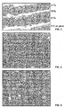
- Figure 1 One embodiment of a solar cell structure is shown in Figure 1 . As described in more detail below, the structure is a multijunction solar cell comprising thin films of ZnTe/PbTe as the absorber layer or ultrathin films forming ZnTe/PbTe superlattices as the absorber layer.
- ZnTe is a p-type semiconductor and PbTe can be p-type or either n-type depending on its doping.
- a layer of n-type CdS serves as the emitter for this solar cell structure, although alternative materials such as ZnO may also be appropriate for the emitter layer.
- the proposed structure comprises a set of superlattice heterojunction solar cells of different effective bandgaps connected in a series configuration.
- the solar cell module 100 includes a glass substrate 105.
- a conductive bottom contact layer 110 is formed on the glass substrate 105.
- the conductive bottom contact layer 110 is a layer of indium tin oxide (ITO).
- the solar cell module includes a first P-N junction 120 disposed over the substrate 105.
- the first P-N junction includes an n-type emitter layer 121, such as a layer of CdS.
- the P-type absorber layer 122 of the P-N junction 120 preferably includes a superlattice structure, which comprises alternating layers of very thin II-VI and IV-VI layers.
- the absorber layer 122 is formed from alternating layers of ZnTe and PbTe.
- the layers are thin film that, while still exhibiting an effective bandgap between the respective bandgaps of the bulk thickness materials, are not of superlattice thickness (i.e., are not thin enough to exhibit quantum effects).
- each P-N junction can be controlled by varying the thickness of the absorber layer 122 and/or the number of layers of a given thickness that form the absorber layer 122. Assuming that each layer in the superlattice structure is approximately 300 ⁇ thick, an effective absorption thickness of about 1 ⁇ m would require approximately 30 layers.
- the solar cell module includes at least one second P-N junction, such as P-N junction 120A.
- P-N junction 120A like P-N junction 120, includes an N-type CdS emitter layer and a p-type absorber layer formed from a ZnTe/PbTe superlattice.
- An interconnect layer 130 electrically connects the first P-N junction 120 to the second P-N junction 120A.
- the interconnect layer includes conductive islands 135, such as HgTe or CuTe islands, for making the electrical interconnection. These islands can be formed in a grid layout, leaving transparent areas 137 (i.e., areas of wide bandgaps) therebetween for passing the incident light to the P-N junction(s).
- a conductive continuous semi-metallic film layer (e.g., HgTe or CuTe) is formed but is sufficiently thin such that is it not opaque, i.e., such that is allows for the passing of the incident light.
- the islands 135 are formed by a lithography/etching process familiar to those in the art.
- a translucent material such as a ZnO x or SiO x can be used to fill the voids 137. If a mechanical connection is to be made between layers, a transparent epoxy can be used in voids 137.
- a conductive transparent layer such as ITO may be used. Tunnel junctions, such as those described in Chaffin et al. may also be appropriate in certain embodiments.
- the solar cell structure can include "n" number of P-N junctions described above connected in series.
- the topmost P-N junction is labeled in FIG. 1 as “120B” and is connected to a P-N junction immediately below by interconnect layer 130A.
- a thin conductive layer 140 such as a layer of HgTe or CuTe, is formed over the final P-N junction and is used to make good contact with a back contact between the backmost absorber layer and layer 150.
- back contact layer 150 is a thicker layer of HgTe or CuTe or graphite paste.
- One significant advantage of a multi-junction solar cell as shown in FIG. 1 is that the resultant spectrum of P-N junction bandgaps can be tailored to fit the incident light spectrum, e.g., the solar spectrum.
- the effective bandgaps of these superlattices of FIG. 1 are adjusted by varying the relative thicknesses of the ZnTe and PbTe layers. Assuming the solar cell structure 100 is a two-cell tandem solar cell, the optimal bandgaps for a two-cell tandem solar cell are 1.0 and 1.8 eV.
- the first P-N junction 120 i.e., that junction closest to the glass substrate 105 and the first P-N junction to be exposed to the light source
- the second P-N junction would be designed to have the narrower bandgap of 1.0 eV.
- the optimal bandgaps are 0.8 eV, 1.4 eV and 2.3 eV.
- the number of p-n junctions that can be included in a solar cell of this invention is essentially unlimited and can be quite large in order to improve the efficiency of the solar cell by matching the different bandgaps to the solar spectrum.
- the number of P-N junctions and their respective bandgaps can be selected such that essentially all of the impinging solar radiation in the U.V. through near infrared range will be absorbed.
- a four-(or more) terminal configuration can be utilized wherein each cell is formed over its own glass substrate and designed to have a respective bandgap.
- two individual cells of different bandgaps are strung together in a four-terminal configuration so that cell-to-cell matching and interfacing between the cells is not an issue.
- the approach used for growing the films of the above-described P-N junctions is a combination of chemical bath deposition for the CdS emitter layer and electrodeposition for the ZnTe and PbTe layers. Both of these techniques are low-cost methods.
- Chemical bath deposition is a well-established technique for the growth of high quality very thin films (approximately 1,000 ⁇ ) of CdS.
- electrodeposited thin film or quantum well structures To date no known work has been performed on using electrodeposited thin film or quantum well structures to prepare and optimize solar cell device structures.
- An important issue for electrodeposition in the past has been scaling of the technique to large areas because of the voltage drop across the surface of the substrate and the critical dependence of the alloy composition on the electroplating potential. This is where the multi-quantum well structure offers a significant advantage in that compounds are used to tune the bandgap of the device rather than ternary alloys of the constituent elements.
- the composition of compounds can be kept constant and this assures reproducibility of film properties.
- a bath containing ions of the constituent metals to be deposited, dissolved in solution is prepared.
- ions of the constituent metals to be deposited For example in the case of depositing ZnTe, Zn 2+ and HTeO 2 + ions are dissolved in solution.
- the working electrode comprises a conducting substrate upon which the thin film is to be deposited.
- a potentiostat/galvanostat can used to apply the desired bias between the working electrode and a counter electrode.
- E E 0 - R ⁇ T n ⁇ F ⁇ ln a ox a red
- E 0 a standard reference potential
- R the universal gas constant (8.314510 J K -1 mol -1 )
- T the absolute temperature
- n the number of electrons transferred in the half-cell reaction
- F the Faraday constant (9.6485309*10 4 C mol -1 )
- a ox and a red are the activities of the oxidizing and reducing species in the bath.
- the activities of the species in the bath, to first order, are equal to the concentrations of the species in the bath.
- the variables in the bath that can be used to control the composition of the films are bath temperature, bath pH, stirring rate, and concentrations of the ions in the bath.
- the deposition current and the applied voltage can also be used to control the composition of the films.
- the quality of the films can also be improved by using very small concentrations of surfactants.
- PbTe and ZnTe films can be electrodeposited from acidic baths at a similar pH of approximately 3 or less.
- Contacts to ZnTe that have ohmic behavior include Cu 2 Te and HgTe, both of which can be electrodeposited.
- the electrodeposition of superlattices can be achieved in one of two different ways.
- the substrate is switched between baths to grow the individual layers.
- the second approach uses a flowing electrolyte that is switched between deposition layers.
- the latter approach has been developed to the point where single atomic layers of the individual elements of compound semiconductors may be grown by employing surface limited reactions.
- the morphology of the deposit can be better controlled in the latter approach and is the preferred technique for the growth of superlattice structures disclosed herein.
- grain size in microcrystalline films Another important consideration in film growth for solar cell applications is grain size in microcrystalline films. It is believed that post-formation heat treatments can be used to optimize cell performance.
- the thin CdS emitter layer should be heat treated in air with or without a CdCl 2 treatment to promote larger grain size. This will help to promote larger grain PbTe and ZnTe films to form on the CdS layer, although further post-deposition heat treatment may also be required. Large grain size is desired to maximize collection efficiency of the photogenerated carriers.
- the first parameter is the concentration of the chemicals. These concentrations were calculated using the basic molarity formula. Then the masses were measured using a sensitive scale. The second parameter that was monitored was the temperature. Temperature plays a significant role in the rate of the chemical change and thus the rate of film deposition. Temperature was measured using a thermometer. The third parameter is the pH, which was monitored using a pH meter. The last two parameters were the deposition current and the applied voltage.
- ITO indium tin oxide
- the substrate was placed in an ultrasonic bath in 2% Micro 8790 detergent solution for twenty minutes.
- the Micro 8790 detergent solution recommends 75ml of detergent for every gallon of water.
- the bath included approximately 2 ml detergent for 100 ml deionized water.
- the substrate was then placed in an ultrasonic bath of de-ionized water rinse for 20 minutes, followed by a 5 minutes acetone bath and a 5 minute methanol bath.
- the substrate was then blow dried with N 2 gas.
- N 2 gas was then blow dried with N 2 gas.
- Cadmium Sulfide was deposited on the ITO-coated glass substrate using chemical bath deposition. This process is dependent upon the careful mixing of certain chemical reactants and their interaction with a glass surface. It is important to control the rate of these reactions so that they occur slowly enough to allow the CdS to form gradually on the substrate or to diffuse and adhere either to the substrate itself or to the growing film, rather than aggregate into larger particles in solution and precipitate out. This rate can be controlled by the temperature, pH and/or the concentration of sulfide forming precursors in the bath.
- the composition of a deposited CdS film was analyzed using a scanning electron microscope. It was observed that Cd and S were deposited in equal stoichiometric proportions on the ITO-coated glass substrate. In order to confirm the type of the deposited material, optical characterization tests were also performed. The data obtained showed that the material had a bandgap of 2.41 eV, which is very close to the expected 2.4 eV CdS bandgap.
- FIG. 2 A schematic diagram of a basic electrodeposition set up 200 used for electrodepositing a ZnTe film is shown in FIG. 2 .
- the working electrode 210 is the conducting substrate upon which the thin film is to be deposited. In the experiments, the conducting substrate was an indium tin oxide (ITO)-coated glass substrate.
- ITO indium tin oxide
- a potentiostat/galvanostat 220 was used to apply a bias between the working electrode 210 and a counter electrode 230.
- the counter electrode 230 was a Zn foil.
- a ZnTe film deposited on the CdS layer in the proposed solar cell structure serves as the first layer of the superlattice of the p-type absorber layer of the P-N junction 120.
- ZnTe in bulk form thicknesses, has a bandgap of 2.29 eV.
- ZnTe can be deposited as a p-type or an n-type film depending on the voltage applied in the electrodeposition process. In the preferred structure shown in FIG. 1 , the film is p-type.
- TeO 2 was speciated in NaOH. Also, ZnCl 2 was dissolved using deionized water. TeO 2 was added to a heated bath of deionized water. The pH was adjusted to the desired level by adding drops of concentrated HCl. ZnCl 2 was added slowly to the solution.
- the deposition method used short circuit electrodeposition where the cathode is connected directly to the anode to facilitate electron transfer.
- a two electrode cell configuration [wire cathode-solution-anode-wire-glass] was used. The ITO-coated cathode was placed 2 cm away from the zinc foil anode, both submerged in the bath. The zinc foil and the substrate were short circuited by soldering an indium wire on the ITO-glass and secured with Kapton tape. The wire can be either spot welded or attached to the anode with an alligator clip.
- FIG. 8 is a timing diagram of the pulsed voltage used in the experiment.
- v/s counter electrode means that the 0 V is being applied between the counter and the working electrodes.
- v/s open circuit means that the potential on the working electrode will be with respect to the solution/bath, and not the counter electrode. But this voltage is still between the same two electrodes. That is, the pulsed voltage is between the working electrode and the counter electrode, at all times, but its value/amplitude is different. And it is that difference in the applied voltage that is represented, and not any change in the connections. The connection is between the working and counter electrode.
- Table 3.0 shows a summary of the preferred parameters for depositing a ZnTe film of about 0.2-0.4 ⁇ m in thickness.
- the film was initially a light golden/amber color and turned darker with time. The film did not come off when rinsed with water and thus showed good adherence to the glass.
- a PbTe film is deposited on the ZnTe layer in the proposed solar cell structure 100 and serves as the second layer of the thin film or superlattice structure of the p-type absorber layer of the P-N junction 120.
- PbTe has a bandgap of 0.29 eV.
- PbTe can be deposited as a p-type film or an n-type depending on the voltage applied in the experiment. In the structure of FIG. 1 , PbTe is deposited as p-type film.
- FIG. 9 is a timing diagram of the pulsed voltage used in the experiment.
- the electrodeposition set up 200 of FIG. 2 was used.
- the working electrode /cathode 210 upon which the thin film was to be deposited was again an ITO-coated glass substrate.
- the counter electrode 230 was graphite carbon.
- a potentiostat/galvanostat 220A was used to apply a bias between the working electrode 210 and a counter electrode 230.
- TeO 2 was speciated with NaOH and then added to deionized water.
- Pb(NO 3 ) 2 was dissolved in deionized water. Drops of HNO 3 were added to adjust the pH of the solution. Upon addition of the Pb(NO 3 ) 2 to the solution, small white particles were observed and the solution became heterogeneous.
- the bath was heated. Upon stabilization of the bath, an electrode cell was inserted as shown in FIG. 2 , and a pulsed voltage as shown in FIG. 9 was applied.
- the film deposited immediately and rapidly. The film had a homogeneous growth. Very small holes appeared on the film which disappeared later. The film had good adherence and reflectivity. It was light grey in color.
- Table 4.0 A summary of the parameters that produced the best film are listed in Table 4.0 below.
- absorber layers formed using thin film layers of ZnTe/PbTe can have effective bandgaps between the respective bandgaps of bulk thickness ZnTe and PbTe.
- this shows that even at thin film (but not yet superlattice thicknesses), the thicknesses of the layers can be used to control the effective bandgap of a stacked structure. Nonetheless, providing films of ZnTe and PbTe in the order of nanometers is required to obtain the quantum well effects.
- These superlattice structures will afford even greater control of the resultant effective bandgap of the stacked structure as well as more effective absorption of the incident light.
- One of the parameters that can be used to control the thickness of the thin film deposition is the current. Having a low deposition current causes the film to deposit very slowly. Therefore, by depositing the films for a short time a low thickness can be obtained.
- the deposition current can be regulated by the pH and the temperature of the bath.
- the ZnTe film observed under the SEM showed that the film grows in an aggregate fashion where one grain deposits on the substrate and then the other Zn and Te atoms become attached to it until the overall film forms.
- the images showed white and black particles, which indicates the presence of two types of molecules.
- a SEM view of this ZnTe film at 100,000x magnification is shown in FIG. 4 .
- the heavy molecules are indicated in black and the light molecules are represented in white. Since the atomic weight of Pb (127) is almost double that of Zn (66), it is believed that Pb is represented in black and Zn is represented in white.
- the average grain size of the film was determined to be around 120 nm.
- the PbTe film observed using SEM showed that the electrodeposited film was highly compact. This means that the film is highly uniform.
- the average grain size of the film was around 100 nm.
- An SEM view of the PbTe film at 100,000x magnification is shown in FIG. 5 .
- EDS Energy Dispersive Spectrometry
- the EDS measurements showed that the CdS film consisted of 52% by weight of Cd and 48% by weight of S.
- the calculated atomic percentages of the Cd and S were 56% and 44%, respectively.
- the EDS measurements showed that the ZnTe film consisted of 48% by weight Zn and 52% by weight Te.
- the calculated atomic percentage of Zn was 62% and the atomic percentage of Tc was 38%.
- the value hv represents photon energy.
- Plotting ( ⁇ hv ) 1/2 v. photon energy reveals whether the material is a direct or indirect bandgap material. It also allows for determination of the effectiveness of the light absorption.
- the measured bandgap of the deposited ZnTe film was 2.1 eV, which is very close to the 2.25 eV.
- the curve had to be extrapolated beyond the 1.13 to 3.68 eV region that was provided by the measurements.
- PbTe has a bandgap of 0.29 eV, which lies in the infrared region.
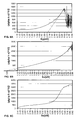
- the spectrophotometer did not provide measurements in that region. So in order to get an estimate of the PbTe bandgap, the curve was extrapolated until it intersected the x-axis. The value obtained as the result of extrapolation was 0.5 eV as shown in FIG. 6B .
- the CdS film had a bandgap of 2.41 eV as shown in FIG. 6C .
- the bandgap of the ZnTe/PbTe composite was 1.26 eV as shown in FIG. 6D and that of the ZnTe/PbTe/ZnTe structure was 1.13 eV as shown in figure 6E . Although it seems that there is a shift in the bandgap between the two structures, this shift is not due to the quantum effect, but rather is an average of the bandgap of the two materials. The quantum effect will only be observed if the thickness of the film is in the order of a few nanometers.
- thermopower test is an easy technique used to determine the conductivity type of material deposited based on comparing the potential of one known film type to another unknown. It has been shown in the literature that CdS deposits as an n-type material. In order to measure the potential across the as-deposited CdS film a voltmeter was used and a temperature gradient was applied. The temperature gradient was created by heating one terminal of the voltmeter with a soldering iron and placing it on the glass and holding the other terminal on the film. After a few seconds the voltmeter read - 6mV. The same procedure was applied on the ZnTe film. The voltmeter read 2mV, which indicates that the ZnTe film deposited is p-type. The same technique was also used to determine the conductivity type of the PbTe film. The voltmeter read 4 mV, which indicated that the PbTe film deposited is p-type.
- a ZnTe/PbTe structure was formed for testing purposes.
- the first film deposited was zinc telluride followed by a lead telluride film. The deposition procedure is described below.
- the deposition parameters described above for forming lattice structures having ZnTe and PbTe layers in the 0.2-0.4 ⁇ m thickness range were also used to form stacked ZnTe/PbTe structures, testing of which is ongoing. Pulsed, rather than direct voltage, was used in order to obtain thinner films.
- a solar cell for testing was also fabricated by depositing a layer of CdS on the ITO coated glass as described above.
- the film showed chemical and optical properties as described above.
- a ZnTe/PbTe/ZnTe structure was deposited on top of the CdS.
- the layers were covered with silver paint that would act as a contact as shown in FIG. 7 .
- the cell was subjected to a light beam from a light projector and connected to a multi-meter.
- the multi-meter was connected as an ammeter to the solar cell in order to measure the short circuit current. After about 3 minutes, current of the order of few ⁇ A passed through the ammeter.
- the multi-meter was then connected as a voltmeter to the cell to read the open circuit voltage.
- the open circuit voltage was 0.05 mV.
- lead telluride and zinc telluride thin films were deposited electrochemically from aqueous solutions.
- Cadmium sulfide layers were deposited using chemical bath deposition.
- the chemical composition of the films was analyzed using scanning electron microscopy (SEM).
- SEM scanning electron microscopy
- the optical bandgap was determined by optical absorption spectroscopy.
- PbTe and ZnTe films were found to have equal stoichiometric proportions of Pb and Te, and of Zn and Te.
- the chemical composition was analyzed using energy dispersive spectroscopy (EDS).
- EDS energy dispersive spectroscopy
- the bandgap of the PbTe and ZnTe were found to be 0.5 and 2.1 eV respectively.
- the developed films had polycrystalline randomly-oriented structure.
- the average grain size of the materials was around 100-120 nm in diameter.
- a lattice structure consisting of ZnTe/PbTe and ZnTe/PbTe/ZnTe were also developed and exhibited bandgaps of 1.26 eV and 1.13 eV, respectively.
- a working solar cell was also developed from the deposited thin films. Modifications to the film thicknesses of PbTe and ZnTe layers can be used to change the bandgap of the structure to customize individual P-N junctions in a multi-junction solar cell structure to provide for efficient conversion of an incident spectrum to electrical energy.
Landscapes
- Engineering & Computer Science (AREA)
- Chemical & Material Sciences (AREA)
- Nanotechnology (AREA)
- Life Sciences & Earth Sciences (AREA)
- Physics & Mathematics (AREA)
- Biophysics (AREA)
- Optics & Photonics (AREA)
- Crystallography & Structural Chemistry (AREA)
- Photovoltaic Devices (AREA)
- Sustainable Development (AREA)
- Sustainable Energy (AREA)
Claims (16)
- Stapelsolarzelle (100), umfassend:mindestens zwei p-n-Übergänge (120, 120A, 120B), die elektrisch in Reihe miteinander verbunden sind, wobei jeder p-n-Übergang (120, 120A, 120B) eine p-leitende Absorberschicht (122) und eine n-leitende Emitterschicht (121) umfasst, wobei jede p-leitende Absorberschicht (122) eine Vielzahl von sich abwechselnden Dünnfilmschichten aus II-VI- und IV-VI-Materialien umfasst, wobei die II-VI- und IV-VI-Materialien jeweilige Bandlücken haben, wenn sie die Massendicke haben, und die effektive Bandlücke von jeder p-leitenden Absorberschicht zwischen den jeweiligen Bandlücken liegt,wobei die effektive Bandlücke der Absorberschicht (122) eines ersten der mindestens zwei p-n-Übergänge (120, 120A, 120B) von derjenigen der Absorberschicht (122) eines zweiten der mindestens zwei p-n-Übergänge (120, 120A, 120B) verschieden ist.
- Stapelsolarzelle nach Anspruch 1, bei der die n-leitende Emitterschicht (121) eine Schicht aus Cadmiumsulfid ist.
- Stapelsolarzelle nach einem der Ansprüche von 1 bis 2, die ferner ein Glassubstrat (105) umfasst, das mit einer leitfähigen Schicht (110) beschichtet ist.
- Stapelsolarzelle nach Anspruch 3, bei der die leitfähige Schicht (110) eine Schicht aus Indiumzinnoxid umfasst.
- Stapelsolarzelle nach einem der Ansprüche von 1 bis 4, die ferner eine Verbindungsschicht (130, 130A) umfasst, die zwischen den p-n-Übergängen (120, 120A, 120B) angeordnet ist und sie miteinander elektrisch verbindet, wobei die Verbindungsschicht (130, 130A) eine Vielzahl von leitfähigen Inseln (135) umfasst.
- Stapelsolarzelle nach Anspruch 5, bei der die leitfähigen Inseln (135) Quecksilbertellurid- oder Kupfertellurid-Inseln umfassen.
- Stapelsolarzelle nach einem der Ansprüche von 1 bis 6,
wobei die Stapelsolarzelle eine Zweizellen-Tandemsolarzelle ist, bei der die effektive Bandlücke der Absorberschicht (122) des ersten der p-n-Übergänge (120, 120A, 120B) ungefähr 1,0 eV beträgt und die effektive Bandlücke der Absorberschicht (122) des zweiten der p-n-Übergänge (120, 120A, 120B) ungefähr 1,8 eV beträgt, oder
wobei die Stapelsolarzelle eine Dreizellen-Tandemsolarzelle ist, bei der die effektive Bandlücke der Absorberschicht (122) des ersten der p-n-Übergänge (120, 120A, 120B) ungefähr 0,8 eV beträgt, die effektive Bandlücke der Absorberschicht (122) des zweiten der p-n-Übergänge (120, 120A, 120B) ungefähr 1,4 eV beträgt und die effektive Bandlücke der Absorberschicht (122) eines dritten der p-n-Übergänge (120, 120A, 120B) ungefähr 2,3 eV beträgt. - Stapelsolarzelle nach einem der Ansprüche von 1 bis 7, bei der die sich abwechselnden Dünnfilmschichten ein Kompositionsübergitter bilden.
- Stapelsolarzelle nach Anspruch 8, bei der jedes Kompositionsübergitter zwischen 30 und 40 sich abwechselnde Schichten aus Zinktellurid und Bleitellurid umfasst, und bei der jedes Kompositionsübergitter eine effektive Absorptionsdicke zwischen ungefähr 1 und ungefähr 5 µm hat und jede der sich abwechselnden Schichten aus Zinktellurid und Bleitellurid eine Dicke zwischen ungefähr 100 und ungefähr 1000 Å hat.
- Stapelsolarzelle nach einem der Ansprüche von 1 bis 9, bei der die effektiven Bandlücken der Absorberschichten (122) von den Dicken der sich abwechselnden Schichten aus den II-VI- und IV-VI-Materialien in den p-n-Übergängen abhängen.
- Stapelsolarzelle nach einem der Ansprüche von 1 bis 10, bei der die effektive Bandlücke der Absorberschicht des ersten der mindestens zwei p-n-Übergänge ausgewählt ist, um Wellenlängen einfallenden Lichts von ungefähr 0,5 µm einzufangen, und bei der die effektive Bandlücke der Absorberschicht des zweiten der mindestens zwei p-n-Übergänge ausgewählt ist, um Wellenlängen einfallenden Lichts von ungefähr 4,0 µm einzufangen.
- Stapelsolarzelle nach einem der Ansprüche von 1 bis 11, die ferner elektrische Kontakte (110, 150) zum Leiten von Strom aus der Zelle nach ihrer Bestrahlung mit Strahlung, die ein Potential an mindestens einem der p-n-Übergänge erzeugt, umfasst.
- Stapelsolarzelle nach einem der Ansprüche von 1 bis 8 und von 10 bis 12, bei der die II-VI- und IV-VI-Materialien Zinktellurid beziehungsweise Bleitellurid sind.
- Verfahren zur Stromerzeugung, wobei das Verfahren das Aussetzen der Stapelsolarzelle (100) nach einem der Ansprüche von 1 bis 13 an Sonnenstrahlung umfasst.
- Verfahren zum Ausbilden einer Solarzelle (100), das die folgenden Schritte umfasst:Bereitstellen eines Glassubstrats (105);Ausbilden einer Frontkontakt-Schicht auf dem Glassubstrat (110);Ausbilden eines ersten p-n-Übergangs (120), der eine n-leitende Emitterschicht (121) und eine ein Kompositionsübergitter umfassende p-leitende Absorberschicht (122) umfasst, wobei der Schritt des Ausbildens des ersten p-n-Übergangs Folgendes umfasst:galvanisches Abscheiden einer n-leitenden Emitterschicht (121) über die leitfähige Schicht (110);
undgalvanisches Abscheiden einer Vielzahl von sich abwechselnden Schichten aus II-VI- und IV-VI-Materialien,wobei die II-VI- und IV-VI-Materialien jeweilige Bandlücken haben, wenn sie die Massendicke haben, und die effektive Bandlücke der p-leitenden Absorberschicht (122) zwischen den jeweiligen Bandlücken liegt; undAusbilden einer Rückkontakt-Schicht (150) über dem ersten p-n-Übergang. - Verfahren zum Ausbilden einer Solarzelle (100) nach Anspruch 15, wobei die Solarzelle (100) eine Stapelsolarzelle (100) ist, wobei das Verfahren den Schritt des Ausbildens von mindestens einem zweiten p-n-Übergang (120A, 120B) in Reihe mit dem ersten p-n-Übergang (120) umfasst, wobei die effektive Bandlücke der Absorberschicht (122) des ersten p-n-Übergangs (120) von derjenigen der Absorberschicht (122) des zweiten p-n-Übergangs (120A, 120B) verschieden ist.
Applications Claiming Priority (2)
| Application Number | Priority Date | Filing Date | Title |
|---|---|---|---|
| US5229808P | 2008-05-12 | 2008-05-12 | |
| PCT/US2009/043449 WO2009140196A2 (en) | 2008-05-12 | 2009-05-11 | Solar cells and method of making solar cells |
Publications (3)
| Publication Number | Publication Date |
|---|---|
| EP2277192A2 EP2277192A2 (de) | 2011-01-26 |
| EP2277192A4 EP2277192A4 (de) | 2012-10-17 |
| EP2277192B1 true EP2277192B1 (de) | 2014-11-12 |
Family
ID=41319271
Family Applications (1)
| Application Number | Title | Priority Date | Filing Date |
|---|---|---|---|
| EP09747280.7A Not-in-force EP2277192B1 (de) | 2008-05-12 | 2009-05-11 | Solarzellen und herstellungsverfahren für solarzellen |
Country Status (5)
| Country | Link |
|---|---|
| US (1) | US8835752B2 (de) |
| EP (1) | EP2277192B1 (de) |
| CN (1) | CN102089856B (de) |
| ES (1) | ES2530458T3 (de) |
| WO (1) | WO2009140196A2 (de) |
Families Citing this family (11)
| Publication number | Priority date | Publication date | Assignee | Title |
|---|---|---|---|---|
| US8518737B2 (en) * | 2010-09-03 | 2013-08-27 | Board Of Regents, The University Of Texas System | Methods and apparatus for real-time monitoring of cadmium ion during solution growth of cadmium sulfide thin films |
| CN102610685B (zh) * | 2011-03-30 | 2014-07-09 | 郑州大学 | 用于太阳电池的等离子激元增强上转换器及其制备 |
| ES2369300B2 (es) * | 2011-06-21 | 2012-09-13 | Universidad Politécnica de Madrid | Célula solar de banda intermedia con puntos cuánticos no tensionados. |
| US9246434B2 (en) * | 2011-09-26 | 2016-01-26 | First Solar, Inc | System and method for estimating the short circuit current of a solar device |
| US9117956B2 (en) * | 2012-08-31 | 2015-08-25 | First Solar, Inc. | Method of controlling the amount of Cu doping when forming a back contact of a photovoltaic cell |
| US9543457B2 (en) | 2012-09-28 | 2017-01-10 | First Solar, Inc. | Method and system for manufacturing back contacts of photovoltaic devices |
| WO2015084810A2 (en) | 2013-12-05 | 2015-06-11 | The Board Of Regents Of The University Of Oklahoma | Thermophotovoltaic materials, methods of deposition, and devices |
| CN107534066A (zh) * | 2015-02-27 | 2018-01-02 | 密歇根大学董事会 | 具有中间光学滤波器的机械堆叠串列光伏电池 |
| US10593818B2 (en) * | 2016-12-09 | 2020-03-17 | The Boeing Company | Multijunction solar cell having patterned emitter and method of making the solar cell |
| CN108539020A (zh) * | 2018-02-13 | 2018-09-14 | 全球能源互联网研究院有限公司 | 一种分离双结式钙钛矿太阳能电池及其制备方法 |
| CN111531412A (zh) * | 2020-05-08 | 2020-08-14 | 福建省南安市宏炜新材料有限公司 | N-Si基板的抛光工艺 |
Family Cites Families (9)
| Publication number | Priority date | Publication date | Assignee | Title |
|---|---|---|---|---|
| US4688068A (en) * | 1983-07-08 | 1987-08-18 | The United States Of America As Represented By The Department Of Energy | Quantum well multijunction photovoltaic cell |
| US4607272A (en) * | 1983-10-06 | 1986-08-19 | The United States Of America As Represented By The United States Department Of Energy | Electro-optical SLS devices for operating at new wavelength ranges |
| US4950615A (en) * | 1989-02-06 | 1990-08-21 | International Solar Electric Technology, Inc. | Method and making group IIB metal - telluride films and solar cells |
| JP5236847B2 (ja) * | 2001-08-10 | 2013-07-17 | 克巳 岸野 | Ii−vi族化合物半導体結晶および光電変換機能素子 |
| JP5248782B2 (ja) | 2004-01-20 | 2013-07-31 | シリアム・テクノロジーズ・インコーポレーテッド | エピタキシャルに成長させた量子ドット材料を有する太陽電池 |
| US20060207647A1 (en) * | 2005-03-16 | 2006-09-21 | General Electric Company | High efficiency inorganic nanorod-enhanced photovoltaic devices |
| GB0519599D0 (en) | 2005-09-26 | 2005-11-02 | Imp College Innovations Ltd | Photovoltaic cells |
| US7932123B2 (en) * | 2006-09-20 | 2011-04-26 | The Board Of Trustees Of The University Of Illinois | Release strategies for making transferable semiconductor structures, devices and device components |
| US8373060B2 (en) * | 2006-10-24 | 2013-02-12 | Zetta Research and Development LLC—AQT Series | Semiconductor grain microstructures for photovoltaic cells |
-
2009
- 2009-05-11 US US12/991,578 patent/US8835752B2/en not_active Expired - Fee Related
- 2009-05-11 ES ES09747280T patent/ES2530458T3/es active Active
- 2009-05-11 WO PCT/US2009/043449 patent/WO2009140196A2/en not_active Ceased
- 2009-05-11 EP EP09747280.7A patent/EP2277192B1/de not_active Not-in-force
- 2009-05-11 CN CN2009801271474A patent/CN102089856B/zh not_active Expired - Fee Related
Also Published As
| Publication number | Publication date |
|---|---|
| US8835752B2 (en) | 2014-09-16 |
| WO2009140196A2 (en) | 2009-11-19 |
| WO2009140196A3 (en) | 2010-01-07 |
| CN102089856B (zh) | 2013-02-13 |
| CN102089856A (zh) | 2011-06-08 |
| EP2277192A4 (de) | 2012-10-17 |
| US20110155207A1 (en) | 2011-06-30 |
| ES2530458T3 (es) | 2015-03-03 |
| EP2277192A2 (de) | 2011-01-26 |
Similar Documents
| Publication | Publication Date | Title |
|---|---|---|
| US8835752B2 (en) | Solar cells and method of making solar cells | |
| Kumar et al. | Strategic review of secondary phases, defects and defect-complexes in kesterite CZTS–Se solar cells | |
| Sinha et al. | Variations in photovoltaic parameters of CdTe/CdS thin film solar cells by changing the substrate for the deposition of CdS window layer | |
| Olusola et al. | Growth and characterisation of n-and p-type ZnTe thin films for applications in electronic devices | |
| Ojo et al. | Next generation multilayer graded bandgap solar cells | |
| Echendu et al. | Characterization of n-type and p-type ZnS thin layers grown by an electrochemical method | |
| Haneman | Properties and applications of copper indium diselenide | |
| Samantilleke et al. | Growth of n-type and p-type ZnSe thin films using an electrochemical technique for applications in large area optoelectronic devices | |
| Neumann‐Spallart et al. | Photoelectrochemical properties of semiconducting cadmium mercury telluride thin films with bandgaps between 1.47 and 1.08 eV | |
| Olusola | Optoelectronic devices based on graded bandgap structures utiliising electroplated semiconductors | |
| Frick et al. | Observation of [VCu1–In i 2+ VCu1–] Defect Triplets in Cu-Deficient CuInS2 | |
| Kassim et al. | Deposition and characterization of Cu 4 SnS 4 thin films by chemical bath deposition method | |
| Dharmadasa et al. | Electrodeposited p-type and n-type ZnSe layers for light emitting devices and multi-layer tandem solar cells | |
| Chander | Advancement in CdIn2Se4/CdTe based photoelectrochemical solar cells | |
| Hodes et al. | Slurry painted CuInS2 and CuIn5S8 layers: Preparation and photoelectrochemical characterization | |
| Takahashi et al. | Heteroepitaxial growth of CdTe on ap-Si (111) substrate by pulsed-light-assisted electrodeposition | |
| Elsayed et al. | Studies on electrodeposition of zinc selenide and zinc telluride and their photoelectrochemical cell behavior | |
| Oliveri et al. | CuInSe 2/Zn (S, O, OH) junction on Mo foil by electrochemical and chemical route for photovoltaic applications | |
| Silva | High Performance Organic–Inorganic mixed Lead–Tin perovskites for Photovoltaics | |
| Josell et al. | Three dimensionally structured CdTe thin-film photovoltaic devices with self-aligned back-contacts: electrodeposition on interdigitated electrodes | |
| Diso | Research and development of CdTe based thin film PV solar cells | |
| Bastola | CdTe Back Contact Engineering via Nanomaterials, Chemical Etching, Doping, and Surface Passivation | |
| Weerasinghe | Solar cells based on electrodeposited thin films of ZnS, CdS, CdSSe and CdTe | |
| Nakada | Diffusion behavior and microstructural properties of the CBD-ZnS/CIGS interface boundary | |
| Madugu et al. | Synthesis and characterisation of CdTe thin films |
Legal Events
| Date | Code | Title | Description |
|---|---|---|---|
| PUAI | Public reference made under article 153(3) epc to a published international application that has entered the european phase |
Free format text: ORIGINAL CODE: 0009012 |
|
| 17P | Request for examination filed |
Effective date: 20101118 |
|
| AK | Designated contracting states |
Kind code of ref document: A2 Designated state(s): AT BE BG CH CY CZ DE DK EE ES FI FR GB GR HR HU IE IS IT LI LT LU LV MC MK MT NL NO PL PT RO SE SI SK TR |
|
| AX | Request for extension of the european patent |
Extension state: AL BA RS |
|
| DAX | Request for extension of the european patent (deleted) | ||
| A4 | Supplementary search report drawn up and despatched |
Effective date: 20120917 |
|
| RIC1 | Information provided on ipc code assigned before grant |
Ipc: H01L 21/00 20060101AFI20120911BHEP |
|
| 17Q | First examination report despatched |
Effective date: 20140514 |
|
| GRAP | Despatch of communication of intention to grant a patent |
Free format text: ORIGINAL CODE: EPIDOSNIGR1 |
|
| INTG | Intention to grant announced |
Effective date: 20140703 |
|
| GRAS | Grant fee paid |
Free format text: ORIGINAL CODE: EPIDOSNIGR3 |
|
| GRAA | (expected) grant |
Free format text: ORIGINAL CODE: 0009210 |
|
| AK | Designated contracting states |
Kind code of ref document: B1 Designated state(s): AT BE BG CH CY CZ DE DK EE ES FI FR GB GR HR HU IE IS IT LI LT LU LV MC MK MT NL NO PL PT RO SE SI SK TR |
|
| REG | Reference to a national code |
Ref country code: GB Ref legal event code: FG4D |
|
| REG | Reference to a national code |
Ref country code: CH Ref legal event code: EP |
|
| REG | Reference to a national code |
Ref country code: AT Ref legal event code: REF Ref document number: 696200 Country of ref document: AT Kind code of ref document: T Effective date: 20141115 |
|
| REG | Reference to a national code |
Ref country code: IE Ref legal event code: FG4D |
|
| REG | Reference to a national code |
Ref country code: DE Ref legal event code: R096 Ref document number: 602009027711 Country of ref document: DE Effective date: 20141224 |
|
| REG | Reference to a national code |
Ref country code: ES Ref legal event code: FG2A Ref document number: 2530458 Country of ref document: ES Kind code of ref document: T3 Effective date: 20150303 |
|
| REG | Reference to a national code |
Ref country code: NL Ref legal event code: VDEP Effective date: 20141112 |
|
| REG | Reference to a national code |
Ref country code: AT Ref legal event code: MK05 Ref document number: 696200 Country of ref document: AT Kind code of ref document: T Effective date: 20141112 |
|
| PG25 | Lapsed in a contracting state [announced via postgrant information from national office to epo] |
Ref country code: NL Free format text: LAPSE BECAUSE OF FAILURE TO SUBMIT A TRANSLATION OF THE DESCRIPTION OR TO PAY THE FEE WITHIN THE PRESCRIBED TIME-LIMIT Effective date: 20141112 Ref country code: LT Free format text: LAPSE BECAUSE OF FAILURE TO SUBMIT A TRANSLATION OF THE DESCRIPTION OR TO PAY THE FEE WITHIN THE PRESCRIBED TIME-LIMIT Effective date: 20141112 Ref country code: NO Free format text: LAPSE BECAUSE OF FAILURE TO SUBMIT A TRANSLATION OF THE DESCRIPTION OR TO PAY THE FEE WITHIN THE PRESCRIBED TIME-LIMIT Effective date: 20150212 Ref country code: PT Free format text: LAPSE BECAUSE OF FAILURE TO SUBMIT A TRANSLATION OF THE DESCRIPTION OR TO PAY THE FEE WITHIN THE PRESCRIBED TIME-LIMIT Effective date: 20150312 Ref country code: IS Free format text: LAPSE BECAUSE OF FAILURE TO SUBMIT A TRANSLATION OF THE DESCRIPTION OR TO PAY THE FEE WITHIN THE PRESCRIBED TIME-LIMIT Effective date: 20150312 Ref country code: FI Free format text: LAPSE BECAUSE OF FAILURE TO SUBMIT A TRANSLATION OF THE DESCRIPTION OR TO PAY THE FEE WITHIN THE PRESCRIBED TIME-LIMIT Effective date: 20141112 |
|
| PG25 | Lapsed in a contracting state [announced via postgrant information from national office to epo] |
Ref country code: AT Free format text: LAPSE BECAUSE OF FAILURE TO SUBMIT A TRANSLATION OF THE DESCRIPTION OR TO PAY THE FEE WITHIN THE PRESCRIBED TIME-LIMIT Effective date: 20141112 Ref country code: LV Free format text: LAPSE BECAUSE OF FAILURE TO SUBMIT A TRANSLATION OF THE DESCRIPTION OR TO PAY THE FEE WITHIN THE PRESCRIBED TIME-LIMIT Effective date: 20141112 Ref country code: CY Free format text: LAPSE BECAUSE OF FAILURE TO SUBMIT A TRANSLATION OF THE DESCRIPTION OR TO PAY THE FEE WITHIN THE PRESCRIBED TIME-LIMIT Effective date: 20141112 Ref country code: SE Free format text: LAPSE BECAUSE OF FAILURE TO SUBMIT A TRANSLATION OF THE DESCRIPTION OR TO PAY THE FEE WITHIN THE PRESCRIBED TIME-LIMIT Effective date: 20141112 Ref country code: HR Free format text: LAPSE BECAUSE OF FAILURE TO SUBMIT A TRANSLATION OF THE DESCRIPTION OR TO PAY THE FEE WITHIN THE PRESCRIBED TIME-LIMIT Effective date: 20141112 Ref country code: GR Free format text: LAPSE BECAUSE OF FAILURE TO SUBMIT A TRANSLATION OF THE DESCRIPTION OR TO PAY THE FEE WITHIN THE PRESCRIBED TIME-LIMIT Effective date: 20150213 Ref country code: PL Free format text: LAPSE BECAUSE OF FAILURE TO SUBMIT A TRANSLATION OF THE DESCRIPTION OR TO PAY THE FEE WITHIN THE PRESCRIBED TIME-LIMIT Effective date: 20141112 |
|
| PG25 | Lapsed in a contracting state [announced via postgrant information from national office to epo] |
Ref country code: RO Free format text: LAPSE BECAUSE OF FAILURE TO SUBMIT A TRANSLATION OF THE DESCRIPTION OR TO PAY THE FEE WITHIN THE PRESCRIBED TIME-LIMIT Effective date: 20141112 Ref country code: SK Free format text: LAPSE BECAUSE OF FAILURE TO SUBMIT A TRANSLATION OF THE DESCRIPTION OR TO PAY THE FEE WITHIN THE PRESCRIBED TIME-LIMIT Effective date: 20141112 Ref country code: CZ Free format text: LAPSE BECAUSE OF FAILURE TO SUBMIT A TRANSLATION OF THE DESCRIPTION OR TO PAY THE FEE WITHIN THE PRESCRIBED TIME-LIMIT Effective date: 20141112 Ref country code: EE Free format text: LAPSE BECAUSE OF FAILURE TO SUBMIT A TRANSLATION OF THE DESCRIPTION OR TO PAY THE FEE WITHIN THE PRESCRIBED TIME-LIMIT Effective date: 20141112 Ref country code: DK Free format text: LAPSE BECAUSE OF FAILURE TO SUBMIT A TRANSLATION OF THE DESCRIPTION OR TO PAY THE FEE WITHIN THE PRESCRIBED TIME-LIMIT Effective date: 20141112 |
|
| REG | Reference to a national code |
Ref country code: DE Ref legal event code: R097 Ref document number: 602009027711 Country of ref document: DE |
|
| PLBE | No opposition filed within time limit |
Free format text: ORIGINAL CODE: 0009261 |
|
| STAA | Information on the status of an ep patent application or granted ep patent |
Free format text: STATUS: NO OPPOSITION FILED WITHIN TIME LIMIT |
|
| 26N | No opposition filed |
Effective date: 20150813 |
|
| PG25 | Lapsed in a contracting state [announced via postgrant information from national office to epo] |
Ref country code: IT Free format text: LAPSE BECAUSE OF FAILURE TO SUBMIT A TRANSLATION OF THE DESCRIPTION OR TO PAY THE FEE WITHIN THE PRESCRIBED TIME-LIMIT Effective date: 20141112 |
|
| REG | Reference to a national code |
Ref country code: CH Ref legal event code: PL |
|
| PG25 | Lapsed in a contracting state [announced via postgrant information from national office to epo] |
Ref country code: MC Free format text: LAPSE BECAUSE OF FAILURE TO SUBMIT A TRANSLATION OF THE DESCRIPTION OR TO PAY THE FEE WITHIN THE PRESCRIBED TIME-LIMIT Effective date: 20141112 Ref country code: LI Free format text: LAPSE BECAUSE OF NON-PAYMENT OF DUE FEES Effective date: 20150531 Ref country code: CH Free format text: LAPSE BECAUSE OF NON-PAYMENT OF DUE FEES Effective date: 20150531 Ref country code: LU Free format text: LAPSE BECAUSE OF FAILURE TO SUBMIT A TRANSLATION OF THE DESCRIPTION OR TO PAY THE FEE WITHIN THE PRESCRIBED TIME-LIMIT Effective date: 20150511 |
|
| REG | Reference to a national code |
Ref country code: IE Ref legal event code: MM4A |
|
| REG | Reference to a national code |
Ref country code: FR Ref legal event code: ST Effective date: 20160129 |
|
| PG25 | Lapsed in a contracting state [announced via postgrant information from national office to epo] |
Ref country code: SI Free format text: LAPSE BECAUSE OF FAILURE TO SUBMIT A TRANSLATION OF THE DESCRIPTION OR TO PAY THE FEE WITHIN THE PRESCRIBED TIME-LIMIT Effective date: 20141112 |
|
| PG25 | Lapsed in a contracting state [announced via postgrant information from national office to epo] |
Ref country code: IE Free format text: LAPSE BECAUSE OF NON-PAYMENT OF DUE FEES Effective date: 20150511 |
|
| PG25 | Lapsed in a contracting state [announced via postgrant information from national office to epo] |
Ref country code: FR Free format text: LAPSE BECAUSE OF NON-PAYMENT OF DUE FEES Effective date: 20150601 |
|
| PGFP | Annual fee paid to national office [announced via postgrant information from national office to epo] |
Ref country code: ES Payment date: 20160526 Year of fee payment: 8 Ref country code: DE Payment date: 20160527 Year of fee payment: 8 Ref country code: GB Payment date: 20160527 Year of fee payment: 8 |
|
| PG25 | Lapsed in a contracting state [announced via postgrant information from national office to epo] |
Ref country code: MT Free format text: LAPSE BECAUSE OF FAILURE TO SUBMIT A TRANSLATION OF THE DESCRIPTION OR TO PAY THE FEE WITHIN THE PRESCRIBED TIME-LIMIT Effective date: 20141112 |
|
| PG25 | Lapsed in a contracting state [announced via postgrant information from national office to epo] |
Ref country code: HU Free format text: LAPSE BECAUSE OF FAILURE TO SUBMIT A TRANSLATION OF THE DESCRIPTION OR TO PAY THE FEE WITHIN THE PRESCRIBED TIME-LIMIT; INVALID AB INITIO Effective date: 20090511 Ref country code: BG Free format text: LAPSE BECAUSE OF FAILURE TO SUBMIT A TRANSLATION OF THE DESCRIPTION OR TO PAY THE FEE WITHIN THE PRESCRIBED TIME-LIMIT Effective date: 20141112 |
|
| PG25 | Lapsed in a contracting state [announced via postgrant information from national office to epo] |
Ref country code: TR Free format text: LAPSE BECAUSE OF FAILURE TO SUBMIT A TRANSLATION OF THE DESCRIPTION OR TO PAY THE FEE WITHIN THE PRESCRIBED TIME-LIMIT Effective date: 20141112 |
|
| PG25 | Lapsed in a contracting state [announced via postgrant information from national office to epo] |
Ref country code: BE Free format text: LAPSE BECAUSE OF FAILURE TO SUBMIT A TRANSLATION OF THE DESCRIPTION OR TO PAY THE FEE WITHIN THE PRESCRIBED TIME-LIMIT Effective date: 20141112 |
|
| REG | Reference to a national code |
Ref country code: DE Ref legal event code: R119 Ref document number: 602009027711 Country of ref document: DE |
|
| GBPC | Gb: european patent ceased through non-payment of renewal fee |
Effective date: 20170511 |
|
| PG25 | Lapsed in a contracting state [announced via postgrant information from national office to epo] |
Ref country code: GB Free format text: LAPSE BECAUSE OF NON-PAYMENT OF DUE FEES Effective date: 20170511 Ref country code: DE Free format text: LAPSE BECAUSE OF NON-PAYMENT OF DUE FEES Effective date: 20171201 |
|
| PG25 | Lapsed in a contracting state [announced via postgrant information from national office to epo] |
Ref country code: MK Free format text: LAPSE BECAUSE OF FAILURE TO SUBMIT A TRANSLATION OF THE DESCRIPTION OR TO PAY THE FEE WITHIN THE PRESCRIBED TIME-LIMIT Effective date: 20141112 |
|
| REG | Reference to a national code |
Ref country code: ES Ref legal event code: FD2A Effective date: 20180704 |
|
| PG25 | Lapsed in a contracting state [announced via postgrant information from national office to epo] |
Ref country code: ES Free format text: LAPSE BECAUSE OF NON-PAYMENT OF DUE FEES Effective date: 20170512 |