EP2267812A1 - Neue Materialien zur n-Dotierung der Elektronentransportschichten in organischen elektronischen Bauelementen, Verwendung dazu sowie organische elektronische Bauelemente - Google Patents
Neue Materialien zur n-Dotierung der Elektronentransportschichten in organischen elektronischen Bauelementen, Verwendung dazu sowie organische elektronische Bauelemente Download PDFInfo
- Publication number
- EP2267812A1 EP2267812A1 EP10179438A EP10179438A EP2267812A1 EP 2267812 A1 EP2267812 A1 EP 2267812A1 EP 10179438 A EP10179438 A EP 10179438A EP 10179438 A EP10179438 A EP 10179438A EP 2267812 A1 EP2267812 A1 EP 2267812A1
- Authority
- EP
- European Patent Office
- Prior art keywords
- organic electronic
- electronic devices
- phenyl
- naphthyl
- electron transporting
- Prior art date
- Legal status (The legal status is an assumption and is not a legal conclusion. Google has not performed a legal analysis and makes no representation as to the accuracy of the status listed.)
- Granted
Links
Classifications
-
- H—ELECTRICITY
- H10—SEMICONDUCTOR DEVICES; ELECTRIC SOLID-STATE DEVICES NOT OTHERWISE PROVIDED FOR
- H10K—ORGANIC ELECTRIC SOLID-STATE DEVICES
- H10K85/00—Organic materials used in the body or electrodes of devices covered by this subclass
- H10K85/60—Organic compounds having low molecular weight
- H10K85/631—Amine compounds having at least two aryl rest on at least one amine-nitrogen atom, e.g. triphenylamine
- H10K85/633—Amine compounds having at least two aryl rest on at least one amine-nitrogen atom, e.g. triphenylamine comprising polycyclic condensed aromatic hydrocarbons as substituents on the nitrogen atom
-
- H—ELECTRICITY
- H10—SEMICONDUCTOR DEVICES; ELECTRIC SOLID-STATE DEVICES NOT OTHERWISE PROVIDED FOR
- H10K—ORGANIC ELECTRIC SOLID-STATE DEVICES
- H10K50/00—Organic light-emitting devices
- H10K50/10—OLEDs or polymer light-emitting diodes [PLED]
- H10K50/14—Carrier transporting layers
- H10K50/16—Electron transporting layers
- H10K50/165—Electron transporting layers comprising dopants
-
- H—ELECTRICITY
- H10—SEMICONDUCTOR DEVICES; ELECTRIC SOLID-STATE DEVICES NOT OTHERWISE PROVIDED FOR
- H10K—ORGANIC ELECTRIC SOLID-STATE DEVICES
- H10K71/00—Manufacture or treatment specially adapted for the organic devices covered by this subclass
- H10K71/30—Doping active layers, e.g. electron transporting layers
-
- H—ELECTRICITY
- H10—SEMICONDUCTOR DEVICES; ELECTRIC SOLID-STATE DEVICES NOT OTHERWISE PROVIDED FOR
- H10K—ORGANIC ELECTRIC SOLID-STATE DEVICES
- H10K85/00—Organic materials used in the body or electrodes of devices covered by this subclass
- H10K85/60—Organic compounds having low molecular weight
- H10K85/631—Amine compounds having at least two aryl rest on at least one amine-nitrogen atom, e.g. triphenylamine
- H10K85/636—Amine compounds having at least two aryl rest on at least one amine-nitrogen atom, e.g. triphenylamine comprising heteroaromatic hydrocarbons as substituents on the nitrogen atom
-
- H—ELECTRICITY
- H10—SEMICONDUCTOR DEVICES; ELECTRIC SOLID-STATE DEVICES NOT OTHERWISE PROVIDED FOR
- H10K—ORGANIC ELECTRIC SOLID-STATE DEVICES
- H10K85/00—Organic materials used in the body or electrodes of devices covered by this subclass
- H10K85/60—Organic compounds having low molecular weight
- H10K85/649—Aromatic compounds comprising a hetero atom
- H10K85/655—Aromatic compounds comprising a hetero atom comprising only sulfur as heteroatom
-
- Y—GENERAL TAGGING OF NEW TECHNOLOGICAL DEVELOPMENTS; GENERAL TAGGING OF CROSS-SECTIONAL TECHNOLOGIES SPANNING OVER SEVERAL SECTIONS OF THE IPC; TECHNICAL SUBJECTS COVERED BY FORMER USPC CROSS-REFERENCE ART COLLECTIONS [XRACs] AND DIGESTS
- Y02—TECHNOLOGIES OR APPLICATIONS FOR MITIGATION OR ADAPTATION AGAINST CLIMATE CHANGE
- Y02B—CLIMATE CHANGE MITIGATION TECHNOLOGIES RELATED TO BUILDINGS, e.g. HOUSING, HOUSE APPLIANCES OR RELATED END-USER APPLICATIONS
- Y02B10/00—Integration of renewable energy sources in buildings
- Y02B10/10—Photovoltaic [PV]
-
- Y—GENERAL TAGGING OF NEW TECHNOLOGICAL DEVELOPMENTS; GENERAL TAGGING OF CROSS-SECTIONAL TECHNOLOGIES SPANNING OVER SEVERAL SECTIONS OF THE IPC; TECHNICAL SUBJECTS COVERED BY FORMER USPC CROSS-REFERENCE ART COLLECTIONS [XRACs] AND DIGESTS
- Y02—TECHNOLOGIES OR APPLICATIONS FOR MITIGATION OR ADAPTATION AGAINST CLIMATE CHANGE
- Y02E—REDUCTION OF GREENHOUSE GAS [GHG] EMISSIONS, RELATED TO ENERGY GENERATION, TRANSMISSION OR DISTRIBUTION
- Y02E10/00—Energy generation through renewable energy sources
- Y02E10/50—Photovoltaic [PV] energy
- Y02E10/549—Organic PV cells
-
- Y—GENERAL TAGGING OF NEW TECHNOLOGICAL DEVELOPMENTS; GENERAL TAGGING OF CROSS-SECTIONAL TECHNOLOGIES SPANNING OVER SEVERAL SECTIONS OF THE IPC; TECHNICAL SUBJECTS COVERED BY FORMER USPC CROSS-REFERENCE ART COLLECTIONS [XRACs] AND DIGESTS
- Y10—TECHNICAL SUBJECTS COVERED BY FORMER USPC
- Y10S—TECHNICAL SUBJECTS COVERED BY FORMER USPC CROSS-REFERENCE ART COLLECTIONS [XRACs] AND DIGESTS
- Y10S428/00—Stock material or miscellaneous articles
- Y10S428/917—Electroluminescent
Definitions
- the invention relates to novel materials for improving electron injection and electron transport in organic devices such as organic light emitting diodes (OLEDs), organic field effect transistors (OFETs) and organic solar cells.
- organic devices such as organic light emitting diodes (OLEDs), organic field effect transistors (OFETs) and organic solar cells.
- These materials are precursors and are converted into strong electron donors by the vapor deposition process, so that they cover the electron transport layer or the emitter layer of the OLED by dope coating with the electron transporter in small quantities (called n-doping).
- n-doping This leads to an electronic interaction with the electron transport material or the emitter, whereby such additives facilitate the reduction of the electron transport material or of the emitter material (ie the electron uptake into the LUMO [deepest unoccupied molecular orbital] of the electron transport or emitter material), which would otherwise be exclusively due to the energy of the electric field is effected.
- LUMO deepest unoccupied molecular orbital
- the object of the present invention is therefore to provide a material for improving the electron injection and / or the electron transport in organic components, which increase the disadvantages of the prior art, in particular the lack of stability of the injection and electron transport-promoting effect.
- the injection-promoting and electron-transport-promoting effect can be significantly enhanced by the new materials of the substructures 1 to 3 , and their stability can also be improved by the changed bonding conditions.
- Tetradonorethylene (1a and 2a) or the Tetradonorfulvalene (3a) to synthesize directly and to dope the Elektronenakzeptormatrix therewith.
- the materials of substructures 2 and 3 have good glass-forming properties which also contribute to the enhancement of charge transport and charge transfer, and thus conductivity enhancement of the electron transport / emitter layer.
- novel materials which are suitable for improving the electron transport and the electron injection by chemical interaction with any electron transport and / or emitter layers can thus be used universally in polymer electronic components, including all technologies for the production of organic light emitting diodes (OLEDs), organic Field effect transistors (OFETs) and components based on organic understood photovoltaic devices such as organic solar cells.
- OLEDs organic light emitting diodes
- OFETs organic Field effect transistors
- components based on organic understood photovoltaic devices such as organic solar cells.
- the invention relates to novel materials based on donor carbene intermediates for improving electron injection and electron transport in organic electronic components such as organic light-emitting diodes (OLEDs), organic field-effect transistors (OFETs) and components based on organic photovoltaics, in particular organic solar cells.
- organic electronic components such as organic light-emitting diodes (OLEDs), organic field-effect transistors (OFETs) and components based on organic photovoltaics, in particular organic solar cells.
Landscapes
- Physics & Mathematics (AREA)
- Engineering & Computer Science (AREA)
- Chemical & Material Sciences (AREA)
- Materials Engineering (AREA)
- Spectroscopy & Molecular Physics (AREA)
- Optics & Photonics (AREA)
- Manufacturing & Machinery (AREA)
- Electroluminescent Light Sources (AREA)
- Photovoltaic Devices (AREA)
- Heterocyclic Carbon Compounds Containing A Hetero Ring Having Oxygen Or Sulfur (AREA)
- Heterocyclic Compounds Containing Sulfur Atoms (AREA)
- Nitrogen Condensed Heterocyclic Rings (AREA)
- Organic Low-Molecular-Weight Compounds And Preparation Thereof (AREA)
Abstract
Description
- Die Erfindung betrifft neue Materialien zur Verbesserung der Elektroneninjektion und des Elektronentransportes in organischen Bauelementen wie organischen Leuchtdioden (OLEDs), organischen Feldeffekttransistoren (OFETs) und organischen Solarzellen.
- In den letzten Jahren sind insbesondere für organische Leuchtdioden Materialien bekannt geworden, durch die die Elektroneninjektion sowie der Elektronentransport in OLEDs verbessert wird(Pat.: Novaled GmbH Dresden
DE_10307125_A1 01.08.2004 )
Dies bewirkt zusätzlich eine Absenkung der Betriebsspannung bei gleicher Effizienz der OLED. - Diese Materialien liegen als Precursor vor und werden durch den Aufdampfprozess in starke Elektronendonoren umgewandelt, so dass sie coverdampft mit dem Elektronentransporter in geringer Menge die Elektronentransportschicht bzw. die Emitter-schicht der OLED dotieren (n-Doping genannt). Dies führt zu einer elektronischen Wechselwirkung mit dem Elektronentransportmaterial bzw. dem Emitter, wodurch solche Zusätze die Reduktion des Elektronentransportmaterials bzw. des Emittermaterials (also die Elektronenaufnahme in das LUMO [tiefstes unbesetztes Molekülorbital] des Elektonentransport- bzw. Emittermaterials) erleichtern, was sonst ausschließlich durch die Energie des elektrischen Feldes bewirkt wird. Infolgedessen wird bei schwächerem, elektrischem Feld (das einer geringeren Betriebsspannung entspricht) die gleiche Effizienz erreicht, die ohne diese Materialien nur unter stärkerem elektrischem Feld möglich war.
- Bei den bisherigen bekannten Materialien ist jedoch vor allem die Stabilität und der injektions- und elektronentranportfördernde Effekt noch nicht zufrieden stellend.
- Aufgabe der vorliegenden Erfindung ist es deshalb, ein Material zur Verbesserung der Elektroneninjektion und/oder des Elektronentransportes in organischen Bauelementen zu schaffen, das die Nachteile des Standes der Technik, insbesondere die fehlende Stabilität des injektions- und elektronentransportfördernden- Effekts zu erhöhen.
- Die Lösung der Aufgabe und Gegenstand der Erfindung werden in den Ansprüchen, den Beispielen und der Beschreibung offenbart.
- Erfindungsgemäß kann der injektions- und elektronentranportfördernde Effekt durch die neuen zu beanspruchenden Materialien der Substrukturen 1 - 3 noch wesentlich verstärkt werden und ihre Stabilität durch die geänderten Bindungsverhältnisse ebenfalls verbessert werden.
- Ursachen dafür bilden die Verbrückung der Dialkylaminosubstituenten mit dem aromatischen Kern in Substruktur 1 sowie die neu angewendeten redox-stabilen Triarylamindonoren der Substrukturen 2 und 3, die einerseits durch Umwandlung über einen Carbenmechanismus in einem Hochvakuumprozess zu dimeren Tetradonorethylenen (1a und 2a) bzw. Tetradonorfulvalenen (3a) abreagieren, die in einer Elektronenakzeptormatrix sofort in der Lage sind ein Elektron zu übertragen oder andererseits aus dem Carbenzustand direkt mit der Akzeptormatrix einen elektonen-übertragenden komplexartigen Übergangszustand bilden, der wohl in seiner physikalischen Wirkung, nicht aber in seiner chemischen Struktur charakterisiert werden kann.
- Eine weitere Möglichkeit besteht darin die Tetradonorethylene (1a und 2a) bzw. die Tetradonorfulvalene (3a) direkt zu synthetisieren und die Elektronenakzeptormatrix damit zu dotieren.
- Die Materialien der Substrukturen 2 und 3 besitzen darüber hinaus wegen der Triarylaminsubstituenten gute Glasbildungseigenschaften, die ebenfalls zur Verbesserung des Ladungstransportes und der Ladungsübertragung und damit zur Leitfähigkeitserhöhung der Elektronentransport-/Emitter-Schicht beitragen.
- Substrukturen der Prekursor (Carbenoide):

- X hat die Bedeutung eines Anions bevorzugt von Chlorid und Formiat,
- Y steht für O, S oder N-Ar, wobei Ar bevorzugt Phenyl oder 1-Naphthyl darstellt,
- R bedeutet Alkyl, bevorzugt Methyl,
- Ar1 bis Ar3 stehen für Arylreste, deren Bedeutung unabhängig voneinander bevorzugt Phenyl, 1-Naphthyl und 2-Naphthyl ist.
- Substrukturen der Carbendimere:


- Die neuen Materialien, die geeignet sind den Elektronentransport und die Elektroneninjektion durch chemische Wechselwirkung mit beliebigen Elektronentransport- und/oder Emitterschichten zu verbessern können somit universell in polymerelektronischen Bauelementen erfolgreich eingesetzt werden, darunter werden vorrangig alle Technologien zur Herstellung von organischen Leuchtdioden (OLEDs), organischen Feldeffekttransistoren (OFETs) und Bauelementen auf Basis organischer photovoltaischer Bauelemente wie organische Solarzellen verstanden.
- Synthese durch Vilsmeyerformylierung von 8-Hydroxyjulolidin und Kondensation zum Methinfarbstoff 1 im Überschuss von 8-Hydroxyjulolidin und Zusatz von Kaliumchlorid.

-
- a) Synthese des Michlers-Keton-Typ aus 8-Hydroxyjulolidin und Diethylcarbonat.
- b) Dimerisierung des Michlers-Keton Typ durch Mc Murry Reaktion

-
- a) Synthese von 2-Phenylessigsäurediphenylamid aus Diphenylamin und Phenylessigsäurechlorid
- b) Synthese von 2-Phenylthioessigsäurediphenylamid aus 2-Phenylessigsäurediphenylamid und Lawessons Reagenz.
- c) Synthese von Di-[2-(diphenylamino)-3-phenyl-thien-4-yl]-dimethyl-methan aus 2-Phenylthioessigsäurediphenylamid und 1,5-Dibrom-3,3-dimethyl-pentan-2,4-dion.
- d) Vilsmeyerformylierung des Di-[2-(diphenylamino)-3-phenylthien-4-yl]-dimethyl-methan unter Bildung des Methinfarbstoffes 2 und Anionenaustausch mittels Kaliumchlorid.

-
- a) Synthese des Michlers-Keton-Typ durch Reaktion von Di-[2-(diphenylamino)-3-phenyl-thien-4-yl]-dimethyl-methan 3c mit Diethylcarbonat.
- b) Dimerisierung des Michlers-Keton Typ 4a durch Mc Murry Reaktion.

-
- a) Synthese von 2-Phenylessigsäurephenyl-1-naphthylamid aus Phenyl-1-naphthylamin und Phenylessigsäurechlorid
- b) Synthese von 2-Phenylthioessigsäurephenyl-1-naphthylamid aus 2-Phenylessigsäurephenyl-1-naphthylamid und Lawessons Reagenz.
- c) Synthese von 2-Phenyl-3-mopholino-thioacrylsäurephenyl-1-naphthylamid aus 2-Phenylthioessigsäurephenyl-1-naphthylamid, Morpholin und Orthoameisensäureester.
- d) Synthese von 1,2-Di-[2-(phenyl-1-naphthylamino)-3-phenylthien-5-yl]-ethan-1,2-dion aus 2-Phenyl-3-mopholinothioacryl-säurephenyl-1-naphthylamid und 1,4-Dibrombutan-2,3-dion.
- e) Kondensation von 2,5-Diphenyl-3,4-di-[2-(phenyl-1-naphthyl-amino)-3-phenyl-thien-5-yl]-cyclopentadienon aus 1,2-Di-[2-(phenyl-1-naphthylamino)-3-phenyl-thien-5-yl]-ethan-1,2-dion und 1,3-Diphenylaceton mit Kalium-tert.-butylat.
- f) Reduktion des 2,5-Diphenyl-3,4-di-[2-(phenyl-1-naphthylamino)-3-phenyl-thien-5-yl]-cyclopentadienon zum Carbinol mittels Natriumborhydrid.
- g) Bildung des Methinfarbstoffes 3 aus dem Carbinol 5f mit HCl.

-
- a) Dimerisierung des Michlers-Keton Typ 5e durch Mc Murry Reaktion.

- Die Erfindung betrifft neue Materialien auf Basis von Donorcarbenenintermediaten zur Verbesserung der Elektroneninjektion und des Elektronentransportes in organischen elektronischen Bauelementen wie organischen Leuchtdioden (OLEDs), organischen Feldeffekttransistoren (OFETs) und Bauelementen auf Basis organischer Photovoltaik wie insbesondere organischen Solarzellen.
Claims (6)
- Material zur n-Dotierung der Elektronentransportschicht in organischen elektronischen Bauelementen zumindest eine Komponente gemäß einer der drei unten stehenden Strukturen 1a bis 3a umfassend,
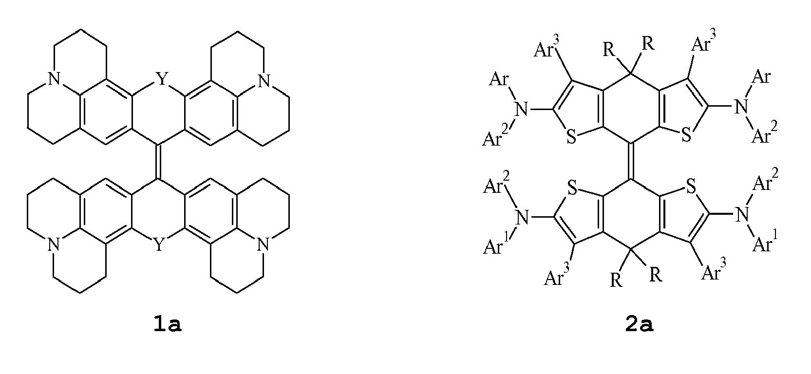
 Y steht für O, S oder N-Ar, wobei Ar bevorzugt Phenyl oder 1-Naphthyl darstellt,R bedeutet Alkyl, bevorzugt Methyl,Ar1 bis Ar3 stehen für Arylreste, deren Bedeutung unabhängig voneinander ist.
 - Material nach Anspruch 1, wobei
R Methyl ist und/oder
Ar1 bis Ar3 beliebig und unabhängig voneinander aus der Gruppe umfassend Phenyl, 1-Naphthyl und 2-Naphthyl ausgewählt ist. - Verfahren zur Herstellung eines Materials nach einem der Ansprüche 1 oder 2 durch Umwandlung der zur den Strukturen 1a bis 3a jeweils korrespondierenden, unten stehenden Strukturen 1 bis 3 in einem Hochvakuumprozess:
 X - hat die Bedeutung eines AnionsY steht für O, S oder N-Ar, wobei Ar bevorzugt Phenyl oder 1-Naphthyl darstellt,R bedeutet Alkyl, bevorzugt Methyl,Ar1 bis Ar3 stehen für Arylreste, deren Bedeutung unabhängig voneinander ist.
 - Verwendung eines Materials nach einem der Ansprüche 1 oder 2 zur n-Dotierung einer Elektronentransportschicht eines organischen elektronischen Bauelements.
- Organisches elektronisches Bauelement zumindest zwei Elektroden mit einer aktiven Schicht umfassend, wobei zwischen zumindest einer Elektrode und der aktiven Schicht eine Elektronentransportschicht angeordnet ist, die mit einem Material nach einem der Ansprüche 1 oder 2 dotiert ist.
- Organisches elektronisches Bauelement nach Anspruch 5, wobei das organisch elektronische Bauelement eine organische Leuchtdiode ist.
Applications Claiming Priority (2)
| Application Number | Priority Date | Filing Date | Title |
|---|---|---|---|
| DE102005042104 | 2005-09-05 | ||
| EP06793040A EP1938399A1 (de) | 2005-09-05 | 2006-08-29 | Neue materialien zur n-dotierung der elektronentransportschichten in organischen elektronischen bauelementen |
Related Parent Applications (1)
| Application Number | Title | Priority Date | Filing Date |
|---|---|---|---|
| EP06793040.4 Division | 2006-08-29 |
Publications (2)
| Publication Number | Publication Date |
|---|---|
| EP2267812A1 true EP2267812A1 (de) | 2010-12-29 |
| EP2267812B1 EP2267812B1 (de) | 2012-01-04 |
Family
ID=37308943
Family Applications (2)
| Application Number | Title | Priority Date | Filing Date |
|---|---|---|---|
| EP10179438A Ceased EP2267812B1 (de) | 2005-09-05 | 2006-08-29 | Neue Materialien zur n-Dotierung der Elektronentransportschichten in organischen elektronischen Bauelementen, Verwendung dazu sowie organische elektronische Bauelemente |
| EP06793040A Ceased EP1938399A1 (de) | 2005-09-05 | 2006-08-29 | Neue materialien zur n-dotierung der elektronentransportschichten in organischen elektronischen bauelementen |
Family Applications After (1)
| Application Number | Title | Priority Date | Filing Date |
|---|---|---|---|
| EP06793040A Ceased EP1938399A1 (de) | 2005-09-05 | 2006-08-29 | Neue materialien zur n-dotierung der elektronentransportschichten in organischen elektronischen bauelementen |
Country Status (6)
| Country | Link |
|---|---|
| US (1) | US8221903B2 (de) |
| EP (2) | EP2267812B1 (de) |
| JP (1) | JP5065276B2 (de) |
| KR (1) | KR101331463B1 (de) |
| CN (1) | CN101268565A (de) |
| WO (1) | WO2007028738A1 (de) |
Families Citing this family (2)
| Publication number | Priority date | Publication date | Assignee | Title |
|---|---|---|---|---|
| DE102012205945A1 (de) * | 2012-04-12 | 2013-10-17 | Siemens Aktiengesellschaft | Organische Superdonoren mit mindestens zwei gekoppelten Carben-Gruppen und deren Verwendung als n-Dotierstoffe |
| CN108516970B (zh) * | 2018-04-25 | 2021-01-19 | 华南理工大学 | 一类杂环桥联苯基乙烯衍生物及其制备方法与应用 |
Citations (4)
| Publication number | Priority date | Publication date | Assignee | Title |
|---|---|---|---|---|
| JP2000103975A (ja) * | 1998-09-28 | 2000-04-11 | Idemitsu Kosan Co Ltd | ローダミン誘導体および色素、色変換膜ならびに有機エレクトロルミネッセンス素子 |
| WO2001091203A2 (en) * | 2000-05-22 | 2001-11-29 | Showa Denko K. K. | Organic electroluminescent device and light-emitting material |
| DE10307125A1 (de) | 2002-02-20 | 2004-01-08 | Novaled Gmbh | Dotiertes organisches Halbleitermaterial sowie Verfahren zu dessen Herstellung |
| EP1394236A1 (de) * | 1997-07-16 | 2004-03-03 | Seiko Epson Corporation | Zusammensetzung für eine Organische LED (OLED) |
Family Cites Families (2)
| Publication number | Priority date | Publication date | Assignee | Title |
|---|---|---|---|---|
| US3932415A (en) * | 1972-04-17 | 1976-01-13 | Eastman Kodak Company | Pyrylium dyes having a fused rigidized nitrogen-containing ring |
| JP4360842B2 (ja) | 2003-06-13 | 2009-11-11 | 株式会社Adeka | ローダミン化合物、これを含有してなるフィルム、画像表示用光学フィルター、色変換層ならびにそれを用いた色変換フィルタおよび色変換発光デバイス |
-
2006
- 2006-08-29 US US12/065,859 patent/US8221903B2/en active Active
- 2006-08-29 WO PCT/EP2006/065752 patent/WO2007028738A1/de not_active Ceased
- 2006-08-29 KR KR1020087007905A patent/KR101331463B1/ko not_active Expired - Fee Related
- 2006-08-29 EP EP10179438A patent/EP2267812B1/de not_active Ceased
- 2006-08-29 CN CNA2006800323707A patent/CN101268565A/zh active Pending
- 2006-08-29 JP JP2008529598A patent/JP5065276B2/ja not_active Expired - Fee Related
- 2006-08-29 EP EP06793040A patent/EP1938399A1/de not_active Ceased
Patent Citations (4)
| Publication number | Priority date | Publication date | Assignee | Title |
|---|---|---|---|---|
| EP1394236A1 (de) * | 1997-07-16 | 2004-03-03 | Seiko Epson Corporation | Zusammensetzung für eine Organische LED (OLED) |
| JP2000103975A (ja) * | 1998-09-28 | 2000-04-11 | Idemitsu Kosan Co Ltd | ローダミン誘導体および色素、色変換膜ならびに有機エレクトロルミネッセンス素子 |
| WO2001091203A2 (en) * | 2000-05-22 | 2001-11-29 | Showa Denko K. K. | Organic electroluminescent device and light-emitting material |
| DE10307125A1 (de) | 2002-02-20 | 2004-01-08 | Novaled Gmbh | Dotiertes organisches Halbleitermaterial sowie Verfahren zu dessen Herstellung |
Non-Patent Citations (2)
| Title |
|---|
| JOHNSON ET AL: "Electroluminescence from single layer molecularly doped polymer films", PURE & APPLIED CHEMISTRY, PERGAMON PRESS, OXFORD, GB, vol. 67, no. 1, 1995, pages 175 - 182, XP002097445, ISSN: 0033-4545 * |
| WERNER A ET AL: "N-TYPE DOPING OF ORGANIC THIN FILMS USING CATIONIC DYES", ADVANCED FUNCTIONAL MATERIALS, WILEY VCH, WIENHEIM, DE, vol. 14, no. 3, March 2004 (2004-03-01), pages 255 - 260, XP001047750, ISSN: 1616-301X * |
Also Published As
| Publication number | Publication date |
|---|---|
| KR20080052635A (ko) | 2008-06-11 |
| KR101331463B1 (ko) | 2013-11-20 |
| US8221903B2 (en) | 2012-07-17 |
| US20080297035A1 (en) | 2008-12-04 |
| JP2009510718A (ja) | 2009-03-12 |
| JP5065276B2 (ja) | 2012-10-31 |
| EP1938399A1 (de) | 2008-07-02 |
| EP2267812B1 (de) | 2012-01-04 |
| WO2007028738A1 (de) | 2007-03-15 |
| CN101268565A (zh) | 2008-09-17 |
Similar Documents
| Publication | Publication Date | Title |
|---|---|---|
| EP3423542B1 (de) | Materialien für organische elektrolumineszenzvorrichtungen | |
| EP3519417B1 (de) | Verbindungen mit diazadibenzofuran- oder diazadibenzothiophen-strukturen | |
| DE112009004294B4 (de) | Materialien für organische Elektrolumineszenzvorrichtungen, deren Verwendung, Verfahren zu deren Herstellung und elektronische Vorrichtung | |
| EP3083880B1 (de) | Heterocyclische spiroverbindungen | |
| EP3519415B1 (de) | Carbazole mit diazadibenzofuran- oder diazadibenzothiophen-strukturen | |
| EP3140302B1 (de) | Materialien für organische elektrolumineszenzvorrichtungen | |
| EP3016959B1 (de) | Polycyclische verbindungen | |
| EP3221294B1 (de) | Heterocyclische verbindungen zur verwendung in elektronischen vorrichtungen | |
| EP3246373B1 (de) | Organische moleküle zur verwendung als emitter | |
| EP2229699B1 (de) | Dithiolenübergangsmetallkomplexe und elektronische oder optoelektronische bauelemente | |
| EP3237409B1 (de) | Carbazole mit zwei dibenzofuran- oder dibenzothiophensubstituenten | |
| WO2015049030A2 (de) | Borenthaltende verbindungen | |
| WO2016102039A1 (de) | Heterocyclische verbindungen mit dibenzazapin-strukturen | |
| DE102008057050A1 (de) | Materialien für organische Elektrolumineszenzvorrichtungen | |
| EP1990847A1 (de) | Verwendung von chinoiden Bisimidazolen und deren Derivaten als Dotand zur Dotierung eines organischen halbleitenden Matrixmaterials | |
| EP3430006A1 (de) | Verbindungen mit spirobifluoren-strukturen | |
| WO2017016667A1 (de) | Verbindungen mit fluoren-strukturen | |
| EP3197887A1 (de) | Heterocyclische verbindungen mit benzo[c]coumarin-strukturen | |
| EP2267812B1 (de) | Neue Materialien zur n-Dotierung der Elektronentransportschichten in organischen elektronischen Bauelementen, Verwendung dazu sowie organische elektronische Bauelemente | |
| EP1938398B1 (de) | Neue materialien zur verbesserung der lochinjektion in organischen elektronischen bauelementen und verwendung des materials | |
| WO2007028712A1 (de) | Materialien zur n-dotierung der elektronentransportschichten in organischen elektronischen bauelementen | |
| EP3911716B1 (de) | Materialien für organische elektrolumineszenzvorrichtungen | |
| WO2017097397A1 (de) | Metallkomplexe |
Legal Events
| Date | Code | Title | Description |
|---|---|---|---|
| PUAI | Public reference made under article 153(3) epc to a published international application that has entered the european phase |
Free format text: ORIGINAL CODE: 0009012 |
|
| AC | Divisional application: reference to earlier application |
Ref document number: 1938399 Country of ref document: EP Kind code of ref document: P |
|
| AK | Designated contracting states |
Kind code of ref document: A1 Designated state(s): DE FR GB |
|
| GRAP | Despatch of communication of intention to grant a patent |
Free format text: ORIGINAL CODE: EPIDOSNIGR1 |
|
| 17P | Request for examination filed |
Effective date: 20110614 |
|
| RIC1 | Information provided on ipc code assigned before grant |
Ipc: H01L 51/00 20060101AFI20110713BHEP |
|
| GRAS | Grant fee paid |
Free format text: ORIGINAL CODE: EPIDOSNIGR3 |
|
| GRAA | (expected) grant |
Free format text: ORIGINAL CODE: 0009210 |
|
| AC | Divisional application: reference to earlier application |
Ref document number: 1938399 Country of ref document: EP Kind code of ref document: P |
|
| AK | Designated contracting states |
Kind code of ref document: B1 Designated state(s): DE FR GB |
|
| REG | Reference to a national code |
Ref country code: GB Ref legal event code: FG4D Free format text: NOT ENGLISH |
|
| REG | Reference to a national code |
Ref country code: DE Ref legal event code: R096 Ref document number: 502006010817 Country of ref document: DE Effective date: 20120308 |
|
| PLBE | No opposition filed within time limit |
Free format text: ORIGINAL CODE: 0009261 |
|
| STAA | Information on the status of an ep patent application or granted ep patent |
Free format text: STATUS: NO OPPOSITION FILED WITHIN TIME LIMIT |
|
| 26N | No opposition filed |
Effective date: 20121005 |
|
| REG | Reference to a national code |
Ref country code: DE Ref legal event code: R097 Ref document number: 502006010817 Country of ref document: DE Effective date: 20121005 |
|
| REG | Reference to a national code |
Ref country code: DE Ref legal event code: R082 Ref document number: 502006010817 Country of ref document: DE Representative=s name: EPPING HERMANN FISCHER, PATENTANWALTSGESELLSCH, DE |
|
| REG | Reference to a national code |
Ref country code: DE Ref legal event code: R082 Ref document number: 502006010817 Country of ref document: DE Representative=s name: EPPING HERMANN FISCHER, PATENTANWALTSGESELLSCH, DE Effective date: 20150209 Ref country code: DE Ref legal event code: R081 Ref document number: 502006010817 Country of ref document: DE Owner name: OSRAM OLED GMBH, DE Free format text: FORMER OWNER: OSRAM OPTO SEMICONDUCTORS GMBH, 93055 REGENSBURG, DE Effective date: 20150209 Ref country code: DE Ref legal event code: R082 Ref document number: 502006010817 Country of ref document: DE Representative=s name: EPPING HERMANN FISCHER PATENTANWALTSGESELLSCHA, DE Effective date: 20150209 |
|
| REG | Reference to a national code |
Ref country code: FR Ref legal event code: PLFP Year of fee payment: 11 |
|
| REG | Reference to a national code |
Ref country code: GB Ref legal event code: 732E Free format text: REGISTERED BETWEEN 20161229 AND 20170104 |
|
| REG | Reference to a national code |
Ref country code: FR Ref legal event code: TP Owner name: OSRAM OLED GMBH, DE Effective date: 20170317 |
|
| REG | Reference to a national code |
Ref country code: FR Ref legal event code: PLFP Year of fee payment: 12 |
|
| PGFP | Annual fee paid to national office [announced via postgrant information from national office to epo] |
Ref country code: GB Payment date: 20170822 Year of fee payment: 12 Ref country code: FR Payment date: 20170822 Year of fee payment: 12 |
|
| GBPC | Gb: european patent ceased through non-payment of renewal fee |
Effective date: 20180829 |
|
| PG25 | Lapsed in a contracting state [announced via postgrant information from national office to epo] |
Ref country code: FR Free format text: LAPSE BECAUSE OF NON-PAYMENT OF DUE FEES Effective date: 20180831 |
|
| PG25 | Lapsed in a contracting state [announced via postgrant information from national office to epo] |
Ref country code: GB Free format text: LAPSE BECAUSE OF NON-PAYMENT OF DUE FEES Effective date: 20180829 |
|
| REG | Reference to a national code |
Ref country code: DE Ref legal event code: R079 Ref document number: 502006010817 Country of ref document: DE Free format text: PREVIOUS MAIN CLASS: H01L0051000000 Ipc: H10K0099000000 |
|
| PGFP | Annual fee paid to national office [announced via postgrant information from national office to epo] |
Ref country code: DE Payment date: 20230823 Year of fee payment: 18 |
|
| REG | Reference to a national code |
Ref country code: DE Ref legal event code: R119 Ref document number: 502006010817 Country of ref document: DE |
|
| PG25 | Lapsed in a contracting state [announced via postgrant information from national office to epo] |
Ref country code: DE Free format text: LAPSE BECAUSE OF NON-PAYMENT OF DUE FEES Effective date: 20250301 |