EP2261997A1 - Photovoltaikvorrichtung und Herstellungsverfahren dafür - Google Patents
Photovoltaikvorrichtung und Herstellungsverfahren dafür Download PDFInfo
- Publication number
- EP2261997A1 EP2261997A1 EP10160250A EP10160250A EP2261997A1 EP 2261997 A1 EP2261997 A1 EP 2261997A1 EP 10160250 A EP10160250 A EP 10160250A EP 10160250 A EP10160250 A EP 10160250A EP 2261997 A1 EP2261997 A1 EP 2261997A1
- Authority
- EP
- European Patent Office
- Prior art keywords
- layer
- flow rate
- rate value
- sub
- light absorbing
- Prior art date
- Legal status (The legal status is an assumption and is not a legal conclusion. Google has not performed a legal analysis and makes no representation as to the accuracy of the status listed.)
- Withdrawn
Links
Images


Classifications
-
- H—ELECTRICITY
- H10—SEMICONDUCTOR DEVICES; ELECTRIC SOLID-STATE DEVICES NOT OTHERWISE PROVIDED FOR
- H10F—INORGANIC SEMICONDUCTOR DEVICES SENSITIVE TO INFRARED RADIATION, LIGHT, ELECTROMAGNETIC RADIATION OF SHORTER WAVELENGTH OR CORPUSCULAR RADIATION
- H10F10/00—Individual photovoltaic cells, e.g. solar cells
-
- H—ELECTRICITY
- H10—SEMICONDUCTOR DEVICES; ELECTRIC SOLID-STATE DEVICES NOT OTHERWISE PROVIDED FOR
- H10F—INORGANIC SEMICONDUCTOR DEVICES SENSITIVE TO INFRARED RADIATION, LIGHT, ELECTROMAGNETIC RADIATION OF SHORTER WAVELENGTH OR CORPUSCULAR RADIATION
- H10F77/00—Constructional details of devices covered by this subclass
- H10F77/10—Semiconductor bodies
- H10F77/16—Material structures, e.g. crystalline structures, film structures or crystal plane orientations
- H10F77/162—Non-monocrystalline materials, e.g. semiconductor particles embedded in insulating materials
- H10F77/166—Amorphous semiconductors
- H10F77/1662—Amorphous semiconductors including only Group IV materials
- H10F77/1668—Amorphous semiconductors including only Group IV materials presenting light-induced characteristic variations, e.g. Staebler-Wronski effect
-
- H—ELECTRICITY
- H10—SEMICONDUCTOR DEVICES; ELECTRIC SOLID-STATE DEVICES NOT OTHERWISE PROVIDED FOR
- H10F—INORGANIC SEMICONDUCTOR DEVICES SENSITIVE TO INFRARED RADIATION, LIGHT, ELECTROMAGNETIC RADIATION OF SHORTER WAVELENGTH OR CORPUSCULAR RADIATION
- H10F10/00—Individual photovoltaic cells, e.g. solar cells
- H10F10/10—Individual photovoltaic cells, e.g. solar cells having potential barriers
- H10F10/17—Photovoltaic cells having only PIN junction potential barriers
-
- H—ELECTRICITY
- H10—SEMICONDUCTOR DEVICES; ELECTRIC SOLID-STATE DEVICES NOT OTHERWISE PROVIDED FOR
- H10F—INORGANIC SEMICONDUCTOR DEVICES SENSITIVE TO INFRARED RADIATION, LIGHT, ELECTROMAGNETIC RADIATION OF SHORTER WAVELENGTH OR CORPUSCULAR RADIATION
- H10F10/00—Individual photovoltaic cells, e.g. solar cells
- H10F10/10—Individual photovoltaic cells, e.g. solar cells having potential barriers
- H10F10/17—Photovoltaic cells having only PIN junction potential barriers
- H10F10/172—Photovoltaic cells having only PIN junction potential barriers comprising multiple PIN junctions, e.g. tandem cells
-
- H—ELECTRICITY
- H10—SEMICONDUCTOR DEVICES; ELECTRIC SOLID-STATE DEVICES NOT OTHERWISE PROVIDED FOR
- H10F—INORGANIC SEMICONDUCTOR DEVICES SENSITIVE TO INFRARED RADIATION, LIGHT, ELECTROMAGNETIC RADIATION OF SHORTER WAVELENGTH OR CORPUSCULAR RADIATION
- H10F71/00—Manufacture or treatment of devices covered by this subclass
-
- H—ELECTRICITY
- H10—SEMICONDUCTOR DEVICES; ELECTRIC SOLID-STATE DEVICES NOT OTHERWISE PROVIDED FOR
- H10F—INORGANIC SEMICONDUCTOR DEVICES SENSITIVE TO INFRARED RADIATION, LIGHT, ELECTROMAGNETIC RADIATION OF SHORTER WAVELENGTH OR CORPUSCULAR RADIATION
- H10F71/00—Manufacture or treatment of devices covered by this subclass
- H10F71/10—Manufacture or treatment of devices covered by this subclass the devices comprising amorphous semiconductor material
- H10F71/103—Manufacture or treatment of devices covered by this subclass the devices comprising amorphous semiconductor material including only Group IV materials
-
- H—ELECTRICITY
- H10—SEMICONDUCTOR DEVICES; ELECTRIC SOLID-STATE DEVICES NOT OTHERWISE PROVIDED FOR
- H10F—INORGANIC SEMICONDUCTOR DEVICES SENSITIVE TO INFRARED RADIATION, LIGHT, ELECTROMAGNETIC RADIATION OF SHORTER WAVELENGTH OR CORPUSCULAR RADIATION
- H10F77/00—Constructional details of devices covered by this subclass
- H10F77/10—Semiconductor bodies
- H10F77/16—Material structures, e.g. crystalline structures, film structures or crystal plane orientations
- H10F77/162—Non-monocrystalline materials, e.g. semiconductor particles embedded in insulating materials
- H10F77/164—Polycrystalline semiconductors
- H10F77/1642—Polycrystalline semiconductors including only Group IV materials
-
- H—ELECTRICITY
- H10—SEMICONDUCTOR DEVICES; ELECTRIC SOLID-STATE DEVICES NOT OTHERWISE PROVIDED FOR
- H10F—INORGANIC SEMICONDUCTOR DEVICES SENSITIVE TO INFRARED RADIATION, LIGHT, ELECTROMAGNETIC RADIATION OF SHORTER WAVELENGTH OR CORPUSCULAR RADIATION
- H10F77/00—Constructional details of devices covered by this subclass
- H10F77/10—Semiconductor bodies
- H10F77/16—Material structures, e.g. crystalline structures, film structures or crystal plane orientations
- H10F77/162—Non-monocrystalline materials, e.g. semiconductor particles embedded in insulating materials
- H10F77/166—Amorphous semiconductors
- H10F77/1662—Amorphous semiconductors including only Group IV materials
-
- Y—GENERAL TAGGING OF NEW TECHNOLOGICAL DEVELOPMENTS; GENERAL TAGGING OF CROSS-SECTIONAL TECHNOLOGIES SPANNING OVER SEVERAL SECTIONS OF THE IPC; TECHNICAL SUBJECTS COVERED BY FORMER USPC CROSS-REFERENCE ART COLLECTIONS [XRACs] AND DIGESTS
- Y02—TECHNOLOGIES OR APPLICATIONS FOR MITIGATION OR ADAPTATION AGAINST CLIMATE CHANGE
- Y02E—REDUCTION OF GREENHOUSE GAS [GHG] EMISSIONS, RELATED TO ENERGY GENERATION, TRANSMISSION OR DISTRIBUTION
- Y02E10/00—Energy generation through renewable energy sources
- Y02E10/50—Photovoltaic [PV] energy
- Y02E10/546—Polycrystalline silicon PV cells
-
- Y—GENERAL TAGGING OF NEW TECHNOLOGICAL DEVELOPMENTS; GENERAL TAGGING OF CROSS-SECTIONAL TECHNOLOGIES SPANNING OVER SEVERAL SECTIONS OF THE IPC; TECHNICAL SUBJECTS COVERED BY FORMER USPC CROSS-REFERENCE ART COLLECTIONS [XRACs] AND DIGESTS
- Y02—TECHNOLOGIES OR APPLICATIONS FOR MITIGATION OR ADAPTATION AGAINST CLIMATE CHANGE
- Y02E—REDUCTION OF GREENHOUSE GAS [GHG] EMISSIONS, RELATED TO ENERGY GENERATION, TRANSMISSION OR DISTRIBUTION
- Y02E10/00—Energy generation through renewable energy sources
- Y02E10/50—Photovoltaic [PV] energy
- Y02E10/548—Amorphous silicon PV cells
-
- Y—GENERAL TAGGING OF NEW TECHNOLOGICAL DEVELOPMENTS; GENERAL TAGGING OF CROSS-SECTIONAL TECHNOLOGIES SPANNING OVER SEVERAL SECTIONS OF THE IPC; TECHNICAL SUBJECTS COVERED BY FORMER USPC CROSS-REFERENCE ART COLLECTIONS [XRACs] AND DIGESTS
- Y02—TECHNOLOGIES OR APPLICATIONS FOR MITIGATION OR ADAPTATION AGAINST CLIMATE CHANGE
- Y02P—CLIMATE CHANGE MITIGATION TECHNOLOGIES IN THE PRODUCTION OR PROCESSING OF GOODS
- Y02P70/00—Climate change mitigation technologies in the production process for final industrial or consumer products
- Y02P70/50—Manufacturing or production processes characterised by the final manufactured product
Definitions
- This application relates to a photovoltaic device and a manufacturing method thereof.
- a photovoltaic device that is to say, a solar cell converts directly sunlight energy into electrical energy.
- the photovoltaic device uses mainly photovoltaic effect of semiconductor junction.
- semiconductor junction when light is incident and absorbed to a semiconductor pin junction formed through a doping process by means of p-type and n-type impurities respectively, light energy generates electrons and holes at the inside of the semiconductor. Then, the electrons and the holes are separated by an internal field so that a photo-electro motive force is generated at both ends of the pin junction.
- electrodes are formed at the both ends of junction and connected with wires, an electric current flows externally through the electrodes and the wires.
- the photovoltaic device includes:
- One aspect of this invention includes a method of manufacturing a photovoltaic device.
- the method includes:
- Another aspect of this invention includes a method of manufacturing a photovoltaic device.
- the method includes:
- Another aspect of this invention includes a method of manufacturing a photovoltaic device.
- the method includes:
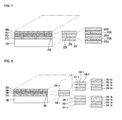
- Fig. 1 shows a photovoltaic device according to a first embodiment of the present invention.
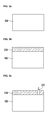
- Fig. 2 shows another photovoltaic device according to a second embodiment of the present invention.
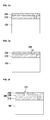
- Figs. 3A to 3H show a manufacturing method of a photovoltaic device according to an embodiment of the present invention.
- Fig. 4 shows a plasma-enhanced chemical vapor deposition apparatus for forming a light absorbing layer according to an embodiment of the present invention.
- Fig. 5 shows a variation of flow rate of source gas for forming a light absorbing layer according to an embodiment of the present invention.
- Fig. 6 shows another variation of flow rate of source gas for forming a light absorbing layer according to an embodiment of the present invention.
- Fig. 7 shows further another variation of flow rate of source gas for forming a light absorbing layer according to an embodiment of the present invention.
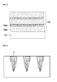
- Fig. 8 shows a light absorbing layer including a plurality of sub-layers included in an embodiment of the present invention.
- Fig. 9 shows a light absorbing layer consisting of a proto-crystalline silicon layer.
- Fig. 1 shows a photovoltaic device according to a first embodiment of the present invention.
- a photovoltaic device includes a substrate 100, a first electrode 210, a second electrode 250, a photoelectric transformation layer 230 and a protecting layer 300.
- the first electrodes 210 are disposed on the substrate 100.
- the first electrodes 210 are spaced from each other at a regular interval in such a manner that adjacent first electrodes are not electrically short-circuited.
- the photoelectric transformation layer 230 is disposed on the first electrode 210 in such a manner as to cover the area spaced between the first electrodes at a regular interval.
- the second electrodes 250 are disposed on the photoelectric transformation layer 230 and spaced from each other at a regular interval in such a manner that adjacent second electrodes are not electrically short-circuited. In this case, the second electrode 250 penetrates the photoelectric transformation layer and is electrically connected to the first electrode 210 such that the second electrode 250 is connected in series to the first electrode 210.
- the adjacent photoelectric transformation layers 230 are spaced at the same interval as the interval between the second electrodes.
- the protecting layer 300 is disposed on the second electrode in such a manner as to cover the area spaced between the second electrodes and the area spaced between the photoelectric transformation layers.
- the photoelectric transformation layer 230 includes a p-type semiconductor layer 231, a light absorbing layer 233 and an n-type semiconductor layer 235.
- the light absorbing layer 233 includes a first sub-layer 233A and a second sub-layer 233B stacked on the first sub-layer 233A.
- the first sub-layer 233A includes a hydrogenated amorphous silicon based material and the second sub-layer 233B includes a crystalline silicon grain.
- Fig. 2 shows another photovoltaic device according to a second embodiment of the present invention.
- the photoelectric transformation layer 230 includes a first photoelectric transformation layer 230-1 and a second photoelectric transformation layer 230-2 disposed on the first photoelectric transformation layer.
- the first photoelectric transformation layer and the second photoelectric transformation layer include p-type semiconductor layers 231-1 and 231-2, light absorbing layers 233-1 and 233-2 and n-type semiconductor layers 235-1 and 235-2.
- the light absorbing layers 233-1 and 233-2 include first sub-layers 233-1A and 233-2A and second sub-layers 233-1B and 233-2B stacked on the first sub-layers.
- the light absorbing layer 233-1 included in the first photoelectric transformation layer 230-1 includes the first sub-layer 233-1A and the second sub-layer 233-1B.
- the first sub-layer 233-1A includes the hydrogenated amorphous silicon based material and the second sub-layer 233-1B includes a crystalline silicon grain.
- the light absorbing layer 233-2 included in the second photoelectric transformation layer 230-2 includes the first sub-layer 233-2A and the second sub-layer 233-2B.
- the first sub-layer 233-2A includes hydrogenated silicon and the second sub-layer 233-2B includes hydrogenated proto-crystalline silicon.
- the second photoelectric transformation layer or the third photoelectric transformation layer can include a light absorbing layer including a first sub-layer and a second sub-layer.
- the first sub-layer includes hydrogenated silicon and the second sub-layer includes hydrogenated proto-crystalline silicon.
- Figs. 3A to 3H show a manufacturing method of a photovoltaic device according to an embodiment of the present invention.
- a substrate 100 is provided first.
- An insulating transparent substrate 100 can be used as the substrate 100.
- a first electrode 210 is formed on the substrate 100.
- the first electrode 210 can be made by chemical vapor deposition (CVD) or be made of transparent conductive oxide (TCO) such as SnO 2 or ZnO.
- CVD chemical vapor deposition
- TCO transparent conductive oxide
- a laser beam is irradiated onto the first electrode 210 or the substrate 100 so that the first electrode 210 is partially removed.
- a first separation groove 220 is formed. That is, since the separation groove 210 penetrates the first electrode 210, preventing adjacent first electrodes from being short-circuited.
- each photoelectric transformation layer 230 including a light absorbing layer is stacked by CVD in such a manner as to cover the first electrode 210 and the first separation groove 220.
- each photoelectric transformation layer 230 includes a p-type semiconductor layer, a light absorbing layer and an n-type semiconductor layer.
- source gas including silicon for example, SiH 4 and source gas including group 3 elements, for example, B 2 H 6 are mixed in a reaction chamber, and then the p-type semiconductor layer is formed by CVD. Then, the source gas including silicon is flown to the reaction chamber so that the light absorbing layer is formed on the p-type semiconductor layer by CVD.
- reaction gas including group 5 element, for example, PH 3 and source gas including silicon are mixed, and then the n-type semiconductor layer is stacked on an intrinsic semiconductor by CVD. Accordingly, the p-type semiconductor layer, the light absorbing layer and the n-type semiconductor layer are stacked on the first electrode 210 in order specified.
- the light absorbing layer according to the embodiment of the present invention can be included in a single junction photovoltaic device including one photoelectric transformation layer 230 or in a multiple junction photovoltaic device including a plurality of photoelectric transformation layers.
- a laser beam is irradiated from the air onto the substrate 100 or the photoelectric transformation layer 230 so that the photoelectric transformation layer 230 is partially removed.
- a second separation groove 240 is hereby formed in the photoelectric transformation layer 230.
- the second electrode 250 is formed by CVD or sputtering process to cover the photoelectric transformation layer 230 and the second separation groove 240.
- a metal layer made of Al or Ag can be used as the second electrode 250.
- a laser beam is irradiated from the air onto the substrate 100 so that the photoelectric transformation layer 230 and the second electrode 250 are partially removed.
- a third separation groove 270 is formed in the photo voltaic layer 230 and the second electrode 250.
- a protecting layer 300 covers partially or entirely a photovoltaic cell 200 including the photoelectric transformation layer 230, the first electrode 210 and the second electrode 250 so as to protect the photovoltaic cell 200.
- the protecting layer 300 can include ethylene Vinyl Acetate (EVA).
- the photoelectric transformation layer 200 having the protecting layer 300 formed thereon.
- a backsheet (not shown) can be made on the protecting layer.
- Fig. 4 shows a plasma-enhanced chemical vapor deposition apparatus for forming a light absorbing layer according to an embodiment of the present invention.
- the first electrode 210 and the p-type semiconductor layer 231 are formed on the substrate 100.
- the substrate 100 is disposed on a plate 300 functioning as an electrode.
- a vacuum pump 320 operates in order to remove impurities in a chamber 310 before the light absorbing layer forming process. As a result, the impurities in the chamber 310 are removed through an angle valve 330 so that the inside of the chamber 310 is actually in a vacuum state.
- source gas such as hydrogen (H 2 ) and silane (SiH 4 ) is flown to the inside of the chamber 310 through mass flow controllers MFC1 and MFC2 and an electrode 340 having a nozzle formed therein. That is, the hydrogen is flown to the chamber through a first mass flow controller MFC1.
- the silane is flown to the chamber through a second mass flow controller MFC2.
- the angle valve 330 is controlled to maintain the pressure of the chamber 310 constant.
- silicon powder caused by a vortex created in the chamber 310 can be prevented from being generated and deposition condition can be maintained constant.
- the hydrogen is flown to the chamber in order to dilute the silane and reduces Staebler-Wronski effect.
- the source gases are flown to the chamber and a voltage from an electric power source E is supplied to the electrode, an electric potential difference is generated between the electrode 340 and the plate 300.
- the source gas is in a plasma state, and the light absorbing layer is deposited on the p-type semiconductor layer 231.
- the flow rate of source gas of silane is controlled in accordance with a deposition time such that at least one sub-layer is formed on the p-type semiconductor layer.
- Fig. 5 shows a variation of flow rate of source gas for forming a light absorbing layer according to an embodiment of the present invention.
- a flow rate A of hydrogen is constant in accordance with the elapse of the deposition time T.
- a flow rate of the silane varies alternately within a range between a first flow rate value ⁇ and a second flow rate value ⁇ in accordance with the elapse of deposition time T.
- the first flow rate value ⁇ and the second flow rate value ⁇ are reduced in accordance with the elapse of deposition time T.
- the duration time t1 of the first flow rate value ⁇ and the duration time t2 of the second flow rate value ⁇ are constant in accordance with the elapse of deposition time T.
- hydrogen and silane can be supplied according to a graph of Fig. 5
- hydrogen and silane can be also supplied according to a graph of Fig. 6 .
- Fig. 6 shows another variation of flow rate of source gas for forming a light absorbing layer according to an embodiment of the present invention.
- the flow rate A of hydrogen is constant in accordance with the deposition time T.
- the flow rate of silane varies alternately within a range between the first flow rate value ⁇ and the second flow rate value ⁇ in accordance with the elapse of deposition time T.
- the duration time t1 of the first flow rate value ⁇ and the duration time t2 of the second flow rate value ⁇ are reduced in accordance with the elapse of deposition time T.
- the first flow rate value ⁇ and the second flow rate value ⁇ are constant in accordance with the elapse of deposition time T.
- hydrogen and silane can be supplied according to a graph of Fig. 5 .
- Fig. 7 shows further another variation of flow rate of source gas for forming a light absorbing layer according to an embodiment of the present invention.
- the flow rate A of hydrogen is constant in accordance with the deposition time T.
- the flow rate of silane varies alternately within a range between the first flow rate value ⁇ and the second flow rate value ⁇ in accordance with the elapse of deposition time T.
- the duration time t1 of the first flow rate value ⁇ and the duration time t2 of the second flow rate value ⁇ are reduced in accordance with the elapse of deposition time T.
- the first flow rate value ⁇ and the second flow rate value ⁇ are reduced in accordance with the elapse of deposition time T.
- the flow rate A of hydrogen is constant in accordance with the deposition time T.
- a ratio of the duration time t1 of the first flow rate value ⁇ to the duration time t2 of the second flow rate value ⁇ is also constant.
- a first sub-layer 233A and a second sub-layer 233B are formed, which have a certain thickness ratio therebetween.
- the flow rate of the silane decreases, varying alternately within a range between the first flow rate value ⁇ and the second flow rate value ⁇ in accordance with the elapse of deposition time T. This will be described later in detail.
- a hydrogen dilution ratio corresponds to a ratio of the flow rate of silane to the flow rate of hydrogen (that is, A/ ⁇ , A/ ⁇ ).
- the first flow rate value ⁇ is greater than the second flow rate value ⁇ . Therefore, a hydrogen dilution ratio during a time period during which the silane with the first flow rate value ⁇ is supplied is less than a hydrogen dilution ratio during a time period during which the silane with the second flow rate value ⁇ is supplied.
- the light absorbing layer 233 including a plurality of the sub-layers 233A and 233B is formed on the p-type semiconductor layer 231 as shown in Fig. 8 .
- the sub-layers 233A and 233B consist of hydrogenated proto-crystalline silicon sub-layer 233B (pc-Si:H) and hydrogenated amorphous silicon sub-layer 233A (a-Si:H).
- the hydrogenated proto-crystalline silicon sub-layer 233B (pc-Si:H) includes a crystalline silicon grain.
- the hydrogenated amorphous silicon sub-layer 233A (a-Si:H) includes amorphous silicon.
- the hydrogenated proto-crystalline silicon based sub-layer 233B is produced during the process of a phase change of the amorphous silicon progress to micro-crystalline silicon.
- the hydrogenated amorphous silicon based sub-layer is referred to as the first sub-layer 233A.
- the hydrogenated proto-crytalline silicon based sub-layer is referred to as the second sub-layer 233B.
- the first sub-layer 233A which is rapidly deposited is formed.
- the first sub-layer 233A includes amorphous silicon.
- the second sub-layer 233B which is deposited slowly is formed.
- the second sub-layer 233B includes a crystalline silicon grain.
- the first sub-layer 233A is formed during a time period during which the silane with the first flow rate value ⁇ is supplied.
- the second sub-layer 233B is formed during a time period during which the silane with the second flow rate value ⁇ is supplied.
- the photovoltaic device according to the embodiment of the present invention can have a high stabilization efficiency.
- the first sub-layer 233A made of an amorphous silicon based material prevents columnar growth of the crystalline silicon grain of the second sub-layer 233B.
- the columnar growth of the crystalline silicon grain is accomplished. That is to say, as deposition is performed, the diameter of the crystalline silicon grain G is increased.
- Such a columnar growth of the crystalline silicon grain increases not only a recombination rate of a carrier such as an electron hole or an electron, but also a time required for the efficiency of the photovoltaic device to reach the stabilization efficiency by crystalline silicon grains having non-uniform diameter. The stabilization efficiency of the photovoltaic device is also reduced.
- the degradation of the light absorbing layer 233 is rapid and the stabilization efficiency is increased.
- the amorphous silicon of the first sub-layer 233A prevents columnar growth of the crystalline silicon grain and has a uniform diameter, so that a time required for the efficiency of the photovoltaic device to reach the stabilization efficiency is reduced and a high stabilization efficiency is obtained.
- the crystalline silicon grains of the second sub-layer 233B are covered with amorphous silicon based material and separated from each other.
- the separated crystalline silicon grain performs a core function of radioactive recombination of a part of captured carriers, preventing photocreation of dangling bond. This reduces non-radioactive recombination of the amorphous silicon based material, which surrounds the crystalline silicon grains, of the second sub-layer 233B.
- the silane cyclically increases and decreases, the more the deposition time T increases, the more the silane remaining in the chamber 310 can increase. Therefore, the hydrogen dilution ratio is reduced and the thicknesses of the first and the second sub-layers 233A and 233B are not maintained constant. It is also difficult to form the crystalline silicon grain of the second sub-layer 233B. As a result, as the flow rate of the silane varies alternately within a range between the first flow rate value ⁇ and the second flow rate value ⁇ , the properties of the light absorbing layer 233 can be degraded.
- the first flow rate value ⁇ and the second flow rate value ⁇ of the silane is reduced in accordance with the elapse of the deposition time T, offsetting the hydrogen dilution ratio's variation caused by the remaining silane.
- the light absorbing layer 233 can be hereby prevented from being degraded.
- the flow rate of hydrogen is constant and the flow rate of silane varies so as to cause the hydrogen dilution ratio to be varied because the flow rate of hydrogen supplied to the inside of the chamber 310 is greater than that of the silane supplied to the inside of the chamber 310, so that it is relatively more difficult to control the flow rate of hydrogen than to control the flow rate of the silane. Therefore, if the flow rate of hydrogen is constant, it is easier to control the hydrogen dilution ratio. In particular, if the flow rate of hydrogen flown to the chamber is constant, a vortex, which is caused by the variation of the flow rate of hydrogen, within the chamber 310 is reduced, improving a film characteristic of the light absorbing layer 233.
- the hydrogen which remains in the chamber 310 increases in accordance with the deposition time T, increasing crystallines of the sub-layers. As a result, it is difficult to form sub-layers having a uniform crystalline diameter and a uniform thickness.
- plasma-enhanced chemical vapor deposition method is used instead of photo-CVD.
- the photo-CVD is not suitable for manufacturing a large area photovoltaic device.
- a thin film is deposited on a quartz window of a photo-CVD device, reducing UV light transmitting the quartz window.
- the plasma-enhanced chemical vapor deposition method can solve the defects of the photo-CVD.
- the crystalline silicon grain having a uniform diameter reduces a time required for the efficiency of the photovoltaic device to reach the stabilization efficiency and improves the stabilization efficiency.
- the hydrogen dilution ratio of the chamber 310 is maintained constant while the second sub-layer 233B of the light absorbing layer 233 is repeatedly deposited.
- the flow rate of hydrogen is constant and a ratio of a time period for supplying the silane with the first flow rate value ⁇ to a time period for supplying the silane with the second flow rate value ⁇ is constant.
- the first and the second flow rate values ⁇ and ⁇ are reduced in accordance with the deposition time in order to offset the remaining silane. Accordingly, the hydrogen dilution ratio within the chamber 310 is maintained constant for the purpose of forming a plurality of the second sub-layers 233B.
- the flow rate of hydrogen is constant and the first and the second flow rate values ⁇ and ⁇ of silane are constant.
- Time periods for supplying the silane with the first and the second flow rate values ⁇ and ⁇ are reduced in accordance with the deposition time in order to offset the remaining silane. Accordingly, an actual hydrogen dilution ratio within the chamber 310 is maintained constant for the purpose of forming a plurality of the second sub-layers 233B.
- a thickness of the first sub-layer 233A made of amorphous silicon can be equal to or more than 10 nm.
- a sum of the thickness of the first sub-layer 233A and the thickness of the second sub-layer 233B, which are formed during one cycle P, can be equal to or less than 50 nm. It is more desirable that the sum is less than 30 nm.
- the thickness of the light absorbing layer 233 including the first and the second sub-layers 233A and 233B can be equal to or more than 150 nm and equal to or less than 350 nm.
- a light absorbing layer 233 can be formed, which has a thickness of 150 nm in three cycles and includes three first sub-layers 233A and three second sub-layers 233B.
- a light absorbing layer 233 having a thickness equal to or more than 150 nm and equal to or less than 350 nm is formed.
- the thickness of the first sub-layer 233A made of amorphous silicon layers is excessively increased. As a result, recombinations in the amorphous silicon layer are increased, degrading a stabilization efficiency.
- a diameter of a crystalline silicon grain can be equal to or more than 3 nm and equal to or less than 10 nm. It is difficult to form a crystalline silicon grain having a diameter less than 3 nm and a degradation rate reduction effect of a solar cell is reduced. If the crystalline silicon grain has a diameter greater than 10nm, the volume of grain boundary in the circumference of the crystalline silicon grain is excessively increased. As a result, the crystalline silicon grain is also increasingly recombined with each other, thereby reducing the efficiency.
- An optical band gap of such a light absorbing layer can be equal to or more than 1.85 eV and equal to or less than 2.0 eV.
- the light absorbing layer 233 according to the embodiment of the present invention has hereby a large optical band gap which is equal to or more than 1.85 eV and equal to or less than 2.0 eV.
- the light absorbing layer can absorb much light with a short wavelength having a high energy density.
- the top cell corresponds to a photoelectric transformation layer on which light is first incident among photoelectric transformation layers that the multiple junction tandem photovoltaic device includes.
- An average hydrogen content of the light absorbing layer 233 including a plurality of the sub-layers 233A and 233B can be equal to or more than 15 atomic % and equal to or less than 25 atomic %. If the average hydrogen content of the light absorbing layer 233 is less than 15 atomic %, the size and density of the quantum dot are reduced, and then the optical band gap of the light absorbing layer 233 can be reduced and the degradation rate of the light absorbing layer 233 can be increased. If the average hydrogen content of the light absorbing layer 233 is greater than 25 atomic %, the diameter of the crystalline silicon grain is excessively increased so that a volume of unstable amorphous silicon is also increased. Accordingly, the degradation rate can be increased.
- a warming-up period WU can be provided before starting to deposit the light absorbing layer 233.
- a voltage is not supplied to the electrode 340 of the chamber 310 during a period of time more than a first cycle P for supplying silane with the first flow rate value ⁇ and the second flow rate value ⁇ .
- the period of time corresponds to the warming-up period.
- a condition inside the chamber 310 may not satisfy the deposition condition of the light absorbing layer 233 even though source gas for forming the light absorbing layer 233 is supplied to the chamber.
- the light absorbing layer 233 can be stably formed.
Landscapes
- Chemical Vapour Deposition (AREA)
- Photovoltaic Devices (AREA)
Applications Claiming Priority (1)
| Application Number | Priority Date | Filing Date | Title |
|---|---|---|---|
| KR1020090052234A KR101100109B1 (ko) | 2009-06-12 | 2009-06-12 | 광기전력 장치의 제조 방법 |
Publications (1)
| Publication Number | Publication Date |
|---|---|
| EP2261997A1 true EP2261997A1 (de) | 2010-12-15 |
Family
ID=42355283
Family Applications (1)
| Application Number | Title | Priority Date | Filing Date |
|---|---|---|---|
| EP10160250A Withdrawn EP2261997A1 (de) | 2009-06-12 | 2010-04-19 | Photovoltaikvorrichtung und Herstellungsverfahren dafür |
Country Status (4)
| Country | Link |
|---|---|
| US (1) | US20100313949A1 (de) |
| EP (1) | EP2261997A1 (de) |
| KR (1) | KR101100109B1 (de) |
| CN (1) | CN101924148A (de) |
Families Citing this family (1)
| Publication number | Priority date | Publication date | Assignee | Title |
|---|---|---|---|---|
| US8557687B2 (en) * | 2009-07-23 | 2013-10-15 | Semiconductor Energy Laboratory Co., Ltd. | Method for forming microcrystalline semiconductor film and method for manufacturing thin film transistor |
Citations (4)
| Publication number | Priority date | Publication date | Assignee | Title |
|---|---|---|---|---|
| JP2004335734A (ja) * | 2003-05-07 | 2004-11-25 | National Institute Of Advanced Industrial & Technology | 薄膜太陽電池 |
| EP1953831A2 (de) * | 2007-01-23 | 2008-08-06 | Sharp Kabushiki Kaisha | Gestapelte photoelektrische Umwandlungsvorrichtung und Herstellungsverfahren dafür |
| WO2008156337A2 (en) * | 2007-06-21 | 2008-12-24 | Jusung Engineering Co., Ltd. | Solar cell, method of fabricating the same and apparatus for fabricating the same |
| JP2009076742A (ja) * | 2007-09-21 | 2009-04-09 | Nissin Electric Co Ltd | 光起電力素子およびその製造方法 |
Family Cites Families (8)
| Publication number | Priority date | Publication date | Assignee | Title |
|---|---|---|---|---|
| JP3037461B2 (ja) * | 1991-05-07 | 2000-04-24 | キヤノン株式会社 | 光起電力素子 |
| US20030044539A1 (en) * | 2001-02-06 | 2003-03-06 | Oswald Robert S. | Process for producing photovoltaic devices |
| US7259321B2 (en) * | 2002-01-07 | 2007-08-21 | Bp Corporation North America Inc. | Method of manufacturing thin film photovoltaic modules |
| EP1918967B1 (de) * | 2006-11-02 | 2013-12-25 | Dow Corning Corporation | Verfahren zur Herstellung einer Schicht durch Abscheidung aus einem Plasma |
| FR2910711B1 (fr) * | 2006-12-20 | 2018-06-29 | Centre Nat Rech Scient | Heterojonction a interface intrinsequement amorphe |
| KR20090120474A (ko) * | 2007-02-12 | 2009-11-24 | 솔라스타, 인코포레이티드 | 고온 캐리어 냉각이 감소된 광전지 셀 |
| US20100258169A1 (en) * | 2009-04-13 | 2010-10-14 | Applied Materials , Inc. | Pulsed plasma deposition for forming microcrystalline silicon layer for solar applications |
| US20110114177A1 (en) * | 2009-07-23 | 2011-05-19 | Applied Materials, Inc. | Mixed silicon phase film for high efficiency thin film silicon solar cells |
-
2009
- 2009-06-12 KR KR1020090052234A patent/KR101100109B1/ko not_active Expired - Fee Related
-
2010
- 2010-04-19 EP EP10160250A patent/EP2261997A1/de not_active Withdrawn
- 2010-04-19 US US12/762,875 patent/US20100313949A1/en not_active Abandoned
- 2010-04-23 CN CN2010101539302A patent/CN101924148A/zh active Pending
Patent Citations (4)
| Publication number | Priority date | Publication date | Assignee | Title |
|---|---|---|---|---|
| JP2004335734A (ja) * | 2003-05-07 | 2004-11-25 | National Institute Of Advanced Industrial & Technology | 薄膜太陽電池 |
| EP1953831A2 (de) * | 2007-01-23 | 2008-08-06 | Sharp Kabushiki Kaisha | Gestapelte photoelektrische Umwandlungsvorrichtung und Herstellungsverfahren dafür |
| WO2008156337A2 (en) * | 2007-06-21 | 2008-12-24 | Jusung Engineering Co., Ltd. | Solar cell, method of fabricating the same and apparatus for fabricating the same |
| JP2009076742A (ja) * | 2007-09-21 | 2009-04-09 | Nissin Electric Co Ltd | 光起電力素子およびその製造方法 |
Non-Patent Citations (3)
| Title |
|---|
| KWAK J ET AL: "Highly and quickly stabilized p-i-n/p-i-n-type protocrystalline silicon multilayer tandem solar cells", SOLAR ENERGY MATERIALS AND SOLAR CELLS, ELSEVIER SCIENCE PUBLISHERS, AMSTERDAM, NL, vol. 92, no. 9, 1 September 2008 (2008-09-01), pages 1067 - 1070, XP022735451, ISSN: 0927-0248, [retrieved on 20080423], DOI: 10.1016/J.SOLMAT.2008.03.010 * |
| KWON S W ET AL: "Characterization of the protocrystalline silicon multilayer", JOURNAL OF NON-CRYSTALLINE SOLIDS, NORTH-HOLLAND PHYSICS PUBLISHING. AMSTERDAM, NL, vol. 352, no. 9-20, 15 June 2006 (2006-06-15), pages 1134 - 1137, XP025187514, ISSN: 0022-3093, [retrieved on 20060615], DOI: 10.1016/J.JNONCRYSOL.2005.12.016 * |
| WRONSKI C R ET AL: "Phase engineering of a-Si:H solar cells for optimized performance", SOLAR ENERGY, PERGAMON PRESS. OXFORD, GB, vol. 77, no. 6, 1 December 2004 (2004-12-01), pages 877 - 885, XP004661828, ISSN: 0038-092X, DOI: 10.1016/J.SOLENER.2004.03.008 * |
Also Published As
| Publication number | Publication date |
|---|---|
| CN101924148A (zh) | 2010-12-22 |
| US20100313949A1 (en) | 2010-12-16 |
| KR20100133602A (ko) | 2010-12-22 |
| KR101100109B1 (ko) | 2011-12-29 |
Similar Documents
| Publication | Publication Date | Title |
|---|---|---|
| EP2273564A2 (de) | Photovoltaikvorrichtung und Herstellungsverfahren dafür | |
| EP3371833B1 (de) | Fotovoltaisches modul und verfahren zur herstellung davon | |
| CN101226967A (zh) | 多结太阳能电池及其形成方法和设备 | |
| KR20080002657A (ko) | 반도체 구조, 태양 전지 및 광 전지 디바이스 제조 방법 | |
| EP3161874B1 (de) | Passivierung von lichtaufnehmenden oberflächen von solarzellen mit kristallinem silicium | |
| WO2013012454A1 (en) | Method of stabilizing hydrogenated amorphous silicon and amorphous hydrogenated silicon alloys | |
| TW202232779A (zh) | 太陽能電池 | |
| JP2001267598A (ja) | 積層型太陽電池 | |
| US8642115B2 (en) | Photovoltaic device and manufacturing method thereof | |
| EP2273563A2 (de) | Photovoltaikvorrichtung und Herstellungsverfahren dafür | |
| EP2261997A1 (de) | Photovoltaikvorrichtung und Herstellungsverfahren dafür | |
| US20250008753A1 (en) | Perovskite solar cell | |
| US20120067416A1 (en) | Photovoltaic Device | |
| US20130291933A1 (en) | SiOx n-LAYER FOR MICROCRYSTALLINE PIN JUNCTION | |
| TW201201396A (en) | Method for manufacturing a solar panel | |
| CN102144296B (zh) | 光伏电池及光伏电池制造方法 | |
| US20120118374A1 (en) | Photovoltaic device | |
| US20120073644A1 (en) | Photovoltaic Device | |
| KR101112494B1 (ko) | 광기전력 장치의 제조 방법 | |
| KR101022822B1 (ko) | 광기전력 장치의 제조 방법 | |
| WO2013034537A2 (en) | Method of manufacturing an intermediate reflector layer |
Legal Events
| Date | Code | Title | Description |
|---|---|---|---|
| PUAI | Public reference made under article 153(3) epc to a published international application that has entered the european phase |
Free format text: ORIGINAL CODE: 0009012 |
|
| 17P | Request for examination filed |
Effective date: 20100419 |
|
| AK | Designated contracting states |
Kind code of ref document: A1 Designated state(s): AT BE BG CH CY CZ DE DK EE ES FI FR GB GR HR HU IE IS IT LI LT LU LV MC MK MT NL NO PL PT RO SE SI SK SM TR |
|
| AX | Request for extension of the european patent |
Extension state: AL BA ME RS |
|
| 17Q | First examination report despatched |
Effective date: 20111005 |
|
| GRAP | Despatch of communication of intention to grant a patent |
Free format text: ORIGINAL CODE: EPIDOSNIGR1 |
|
| STAA | Information on the status of an ep patent application or granted ep patent |
Free format text: STATUS: THE APPLICATION IS DEEMED TO BE WITHDRAWN |
|
| 18D | Application deemed to be withdrawn |
Effective date: 20130625 |