EP2259315A2 - Semiconductor device - Google Patents
Semiconductor device Download PDFInfo
- Publication number
- EP2259315A2 EP2259315A2 EP10005813A EP10005813A EP2259315A2 EP 2259315 A2 EP2259315 A2 EP 2259315A2 EP 10005813 A EP10005813 A EP 10005813A EP 10005813 A EP10005813 A EP 10005813A EP 2259315 A2 EP2259315 A2 EP 2259315A2
- Authority
- EP
- European Patent Office
- Prior art keywords
- semiconductor layer
- island
- type
- layer
- shaped
- Prior art date
- Legal status (The legal status is an assumption and is not a legal conclusion. Google has not performed a legal analysis and makes no representation as to the accuracy of the status listed.)
- Granted
Links
Images























Classifications
-
- H—ELECTRICITY
- H10—SEMICONDUCTOR DEVICES; ELECTRIC SOLID-STATE DEVICES NOT OTHERWISE PROVIDED FOR
- H10B—ELECTRONIC MEMORY DEVICES
- H10B10/00—Static random access memory [SRAM] devices
-
- H—ELECTRICITY
- H10—SEMICONDUCTOR DEVICES; ELECTRIC SOLID-STATE DEVICES NOT OTHERWISE PROVIDED FOR
- H10B—ELECTRONIC MEMORY DEVICES
- H10B10/00—Static random access memory [SRAM] devices
- H10B10/12—Static random access memory [SRAM] devices comprising a MOSFET load element
-
- H—ELECTRICITY
- H10—SEMICONDUCTOR DEVICES; ELECTRIC SOLID-STATE DEVICES NOT OTHERWISE PROVIDED FOR
- H10B—ELECTRONIC MEMORY DEVICES
- H10B99/00—Subject matter not provided for in other groups of this subclass
-
- H—ELECTRICITY
- H10—SEMICONDUCTOR DEVICES; ELECTRIC SOLID-STATE DEVICES NOT OTHERWISE PROVIDED FOR
- H10D—INORGANIC ELECTRIC SEMICONDUCTOR DEVICES
- H10D89/00—Aspects of integrated devices not covered by groups H10D84/00 - H10D88/00
- H10D89/10—Integrated device layouts
Definitions
- the present invention relates to a semiconductor device.
- SGT surrounding gate transistor
- a surrounding gate transistor having a structure in which a source, a gate and a drain are arranged in a direction perpendicular to a substrate, wherein the gate is formed to surround an island-shaped semiconductor layer, and a CMOS inverter circuit using the SGT
- An inverter is constructed using a pMOS transistor and an nMOS transistor.
- a gate width of a pMOS transistor has to be set to be twice as large as that of an nMOS transistor, because a hole mobility is one-half of an electron mobility. Therefore, a conventional CMOS inverter circuit using an SGT (SGT CMOS inverter circuit) is composed of two pMOS SGTs and one nMOS SGT.
- the conventional SGT CMOS inverter circuit is composed of total three island-shaped semiconductors.
- An SRAM is composed of two inverters and two selection transistors.
- an SRAM is constructed using the conventional SGT CMOS inverter circuit, it is composed of four pMOS and four nMOS.
- the SRAM using the conventional SGT CMOS inverter circuit is composed of total eight island-shaped semiconductors.
- a semiconductor device which is characterized by comprising: a first inverter arranged at an intersection of the 1 st row and the 1st column, wherein the first inverter includes a first island-shaped semiconductor layer, a first gate dielectric film in contact with at least a part of a periphery of the first island-shaped semiconductor layer, a first gate electrode having one surface in contact with the first gate dielectric film, a second gate dielectric film in contact with another surface of the first gate electrode, a first arc-shaped semiconductor layer in contact with at least a part of the second gate dielectric film, a first first-conductive-type high-concentration semiconductor layer arranged on a top of the first island-shaped semiconductor layer, a second first-conductive-type high-concentration semiconductor layer arranged underneath the first island-shaped semiconductor layer, a first second-conductive-type high-concentration semiconductor layer arranged on a top of the first arc-shaped semiconductor layer, and a second
- a semiconductor device which is characterized by comprising: a first inverter arranged at an intersection of the 1st row and the 1st column, wherein the first inverter includes a first island-shaped semiconductor layer, a first gate dielectric film surrounding a periphery of the first island-shaped semiconductor layer, a first gate electrode surrounding a periphery of the first gate dielectric film, a second gate dielectric film surrounding a part of a periphery of the first gate electrode, a first arc-shaped semiconductor layer in contact with a part of a periphery of the second gate dielectric film, a first first-conductive-type high-concentration semiconductor layer arranged on a top of the first island-shaped semiconductor layer, a second first-conductive-type high-concentration semiconductor layer arranged underneath the first island-shaped semiconductor layer, a first second-conductive-type high-concentration semiconductor layer arranged on a top of the first arc-shaped semiconductor layer, and a second second-conductive
- a semiconductor device which is characterized by comprising: a first inverter arranged at an intersection of the 1st row and the 1st column, wherein the first inverter includes a first island-shaped semiconductor layer, a first gate dielectric film surrounding a periphery of the first island-shaped semiconductor layer, a first gate electrode surrounding a periphery of the first gate dielectric film, a second gate dielectric film surrounding a part of a periphery of the first gate electrode, a first arc-shaped semiconductor layer in contact with a part of a periphery of the second gate dielectric film, a first first-conductive-type high-concentration semiconductor layer arranged on a top of the first island-shaped semiconductor layer, a second first-conductive-type high-concentration semiconductor layer arranged underneath the first island-shaped semiconductor layer, a first second-conductive-type high-concentration semiconductor layer arranged on a top of the first arc-shaped semiconductor layer, and a second second-conductive
- a semiconductor device which comprises: a first inverter arranged at an intersection of the 1st row and the 1 st column, wherein the first inverter includes a first island-shaped semiconductor layer, a first gate dielectric film surrounding a periphery of the first island-shaped semiconductor layer, a first gate electrode surrounding a periphery of the first gate dielectric film, a second gate dielectric film surrounding a part of a periphery of the first gate electrode, a first arc-shaped semiconductor layer in contact with a part of a periphery of the second gate dielectric film, a first p+-type semiconductor layer arranged on a top of the first island-shaped semiconductor layer, a second p+-type semiconductor layer arranged underneath the first island-shaped semiconductor layer, a first n+-type semiconductor layer arranged on a top of the first arc-shaped semiconductor layer and a second n+-type semiconductor layer arranged underneath the first arc-shaped semiconductor layer;
- a semiconductor device which comprises: a first inverter arranged at an intersection of the 1st row and the 1st column, wherein the first inverter includes a first island-shaped semiconductor layer, a first gate dielectric film surrounding a periphery of the first island-shaped semiconductor layer, a first gate electrode surrounding a periphery of the first gate dielectric film, a second gate dielectric film surrounding a part of a periphery of the first gate electrode, a first arc-shaped semiconductor layer in contact with a part of a periphery of the second gate dielectric film, a first p+-type semiconductor layer arranged on a top of the first island-shaped semiconductor layer, a second p+-type semiconductor layer arranged underneath the first island-shaped semiconductor layer, a first n+-type semiconductor layer arranged on a top of the first arc-shaped semiconductor layer and a second n+-type semiconductor layer arranged underneath the first arc-shaped semiconductor layer; a first inverter arranged at an intersection of the 1s
- the semiconductor device of the present invention is configured to satisfy the following condition: Wp1 ⁇ 2Wn1, wherein Wp1 is an outer peripheral length of the first island-shaped semiconductor layer, and Wn1 is a length of an arc of the first arc-shaped semiconductor layer in contact with a part of the periphery of the second gate dielectric film.
- the semiconductor device of the present invention is configured to satisfy the following condition: Wp2 ⁇ 2Wn2, wherein Wp2 is an outer peripheral length of the second island-shaped semiconductor layer, and Wn2 is a length of an arc of the second arc-shaped semiconductor layer in contact with a part of the periphery of the fourth gate dielectric film.
- the semiconductor device of the present invention is configured to satisfy the following condition: Ln1 ⁇ Lp1, wherein Ln1 is a channel length of the first arc-shaped semiconductor layer, and Lp1 is a channel length of the first island-shaped semiconductor layer.
- the semiconductor device of the present invention is configured to satisfy the following condition: Ln2 ⁇ Lp2, wherein Ln2 is a channel length of the second arc-shaped semiconductor layer, and Lp2 is a channel length of the second island-shaped semiconductor layer.
- a first pMOS transistor, a first nMOS transistor, a second pMOS transistor and a second nMOS transistor are made up of a combination of the first island-shaped semiconductor layer, the first gate dielectric film surrounding the periphery of the first island-shaped semiconductor layer, the first gate electrode surrounding the periphery of the first gate dielectric film, the first p+-type semiconductor layer arranged on the top of the first island-shaped semiconductor layer, and the second p+-type semiconductor layer arranged underneath the first island-shaped semiconductor layer, a combination of the first gate electrode, the second gate dielectric film surrounding a part of the periphery of the first gate electrode, the first arc-shaped semiconductor layer in contact with a part of a periphery of the second gate dielectric film, a first n+-type semiconductor layer arranged on the top of the first arc-shaped semiconductor layer, and the second n+-type semiconductor layer arranged underneath the first arc-shaped semiconductor layer,
- each of the first to tenth semiconductor-metal compound layers is a silicon-metal compound layer.
- the first island-shaped semiconductor layer, the first arc-shaped semiconductor layer, the second island-shaped semiconductor layer, the second arc-shaped semiconductor layer, the third island-shaped semiconductor layer and the fourth island-shaped semiconductor layer may be a first island-shaped silicon layer, a first arc-shaped silicon layer, a second island-shaped silicon layer, a second arc-shaped silicon layer, a third island-shaped silicon layer and a fourth island-shaped silicon layer, respectively.
- each of the n+-type semiconductor layers may be a p+-type silicon layer
- each of the p+-type semiconductor layers may be a p+-type silicon layer.
- the first island-shaped silicon layer, the first arc-shaped silicon layer, the second island-shaped silicon layer, the second arc-shaped silicon layer, the third island-shaped silicon layer and the fourth island-shaped silicon layer are a first n-type or non-doped island-shaped silicon layer, a first p-type or non-doped arc-shaped silicon layer, a second n-type or non-doped island-shaped silicon layer, a second p-type or non-doped arc-shaped silicon layer, a third p-type or non-doped island-shaped silicon layer and a fourth p-type or non-doped island-shaped silicon layer, respectively.
- the semiconductor device comprises: a first inverter arranged at an intersection of the 1st row and the 1st column, wherein the first inverter includes a first island-shaped semiconductor layer, a first gate dielectric film surrounding a periphery of the first island-shaped semiconductor layer, a first gate electrode surrounding a periphery of the first gate dielectric film, a second gate dielectric film surrounding a part of a periphery of the first gate electrode, a first arc-shaped semiconductor layer in contact with a part of a periphery of the second gate dielectric film, a first first-conductive-type high-concentration semiconductor layer arranged on a top of the first island-shaped semiconductor layer, a second first-conductive-type high-concentration semiconductor layer arranged underneath the first island-shaped semiconductor layer, a first second-conductive-type high-concentration semiconductor layer arranged on a top of the first arc-shaped semiconductor layer, and a second second-conductive-type high-concentration semiconductor layer arranged underneath the
- the semiconductor device comprises: a first inverter arranged at an intersection of the 1 st row and the 1st column, wherein the first inverter includes a first island-shaped semiconductor layer, a first gate dielectric film surrounding a periphery of the first island-shaped semiconductor layer, a first gate electrode surrounding a periphery of the first gate dielectric film, a second gate dielectric film surrounding a part of a periphery of the first gate electrode, a first arc-shaped semiconductor layer in contact with a part of a periphery of the second gate dielectric film, a first first-conductive-type high-concentration semiconductor layer arranged on a top of the first island-shaped semiconductor layer, a second first-conductive-type high-concentration semiconductor layer arranged underneath the first island-shaped semiconductor layer, a first second-conductive-type high-concentration semiconductor layer arranged on a top of the first arc-shaped semiconductor layer, and a second second-conductive-type high-concentration semiconductor layer arranged underneath
- the semiconductor device comprises: a first inverter arranged at an intersection of the 1st row and the 1st column, wherein the first inverter includes a first island-shaped semiconductor layer, a first gate dielectric film surrounding a periphery of the first island-shaped semiconductor layer, a first gate electrode surrounding a periphery of the first gate dielectric film, a second gate dielectric film surrounding a part of a periphery of the first gate electrode, a first arc-shaped semiconductor layer in contact with a part of a periphery of the second gate dielectric film, a first p+-type semiconductor layer arranged on a top of the first island-shaped semiconductor layer, a second p+-type semiconductor layer arranged underneath the first island-shaped semiconductor layer, a first n+-type semiconductor layer arranged on a top of the first arc-shaped semiconductor layer and a second n+-type semiconductor layer arranged underneath the first arc-shaped semiconductor layer; a second inverter arranged at an intersection of the 1st row
- the semiconductor device comprises: a first inverter arranged at an intersection of the 1st row and the 1st column, wherein the first inverter includes a first island-shaped semiconductor layer, a first gate dielectric film surrounding a periphery of the first island-shaped semiconductor layer, a first gate electrode surrounding a periphery of the first gate dielectric film, a second gate dielectric film surrounding a part of a periphery of the first gate electrode, a first arc-shaped semiconductor layer in contact with a part of a periphery of the second gate dielectric film, a first p+-type semiconductor layer arranged on a top of the first island-shaped semiconductor layer, a second p+-type semiconductor layer arranged underneath the first island-shaped semiconductor layer, a first n+-type semiconductor layer arranged on a top of the first arc-shaped semiconductor layer and a second n+-type semiconductor layer arranged underneath the first arc-shaped semiconductor layer; a second inverter arranged at an intersection of the 1st row
- the semiconductor device is configured to satisfy the following condition: Wp1 ⁇ 2Wn1, wherein Wp1 is an outer peripheral length of the first island-shaped semiconductor layer, and Wn1 is a length of an arc of the first arc-shaped semiconductor layer in contact with a part of the periphery of the second gate dielectric film.
- a gate length of a pMOS transistor can be set to be twice as large as that of an nMOS transistor. This makes it possible to provide a semiconductor device comprising a highly-integrated SGT-based SRAM.
- the semiconductor device is configured to satisfy the following condition: Wp2 ⁇ 2Wn2, wherein Wp2 is an outer peripheral length of the second island-shaped semiconductor layer, and Wn2 is a length of an arc of the second arc-shaped semiconductor layer in contact with a part of the periphery of the fourth gate dielectric film.
- Wp2 is an outer peripheral length of the second island-shaped semiconductor layer
- Wn2 is a length of an arc of the second arc-shaped semiconductor layer in contact with a part of the periphery of the fourth gate dielectric film.
- a gate length of a pMOS transistor can be set to be twice as large as that of an nMOS transistor. This makes it possible to provide a semiconductor device comprising a highly-integrated SGT-based SRAM.
- the semiconductor device is configured to satisfy the following condition: Ln1 ⁇ Lp1, wherein Ln1 is a channel length of the first arc-shaped semiconductor layer, and Lp1 is a channel length of the first island-shaped semiconductor layer.
- the semiconductor device is configured to satisfy the following condition: Ln2 ⁇ Lp2, wherein Ln2 is a channel length of the second arc-shaped semiconductor layer, and Lp2 is a channel length of the second island-shaped semiconductor layer.
- a first pMOS transistor, a first nMOS transistor, a second pMOS transistor and a second nMOS transistor are made up of a combination of the first island-shaped semiconductor layer, the first gate dielectric film surrounding the periphery of the first island-shaped semiconductor layer, the first gate electrode surrounding the periphery of the first gate dielectric film, the first p+-type semiconductor layer arranged on the top of the first island-shaped semiconductor layer, and the second p+-type semiconductor layer arranged underneath the first island-shaped semiconductor layer, a combination of the first gate electrode, the second gate dielectric film surrounding a part of the periphery of the first gate electrode, the first arc-shaped semiconductor layer in contact with a part of a periphery of the second gate dielectric film, a first n+-type semiconductor layer arranged on the top of the first arc-shaped semiconductor layer, and the second n+-type semiconductor layer arranged underneath the first arc-shaped semiconductor layer, a combination of
- each of the first to tenth semiconductor-metal compound layers is a silicon-metal compound layer.
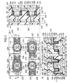
- FIG. 1 shows a semiconductor device according to one embodiment of the present invention, wherein (a), (b) and (c) are a schematic diagram of the semiconductor device in a plane view, a sectional view taken along the line X-X' in (a) and a sectional view taken along the line Y-Y' in (a), respectively.
- (a) is a top plan view in which some part is hatched for distinguishing regions. Some components are hatched in a plane view for distinguishing regions. Only two sectional views of the semiconductor device are shown for the easy of viewing.
- the semiconductor device comprises: a first inverter 237 arranged at an intersection of the 1st row and the 1st column, wherein the first inverter 237 includes a first island-shaped silicon layer 137, a first gate dielectric film 187 surrounding a periphery of the first island-shaped silicon layer 137, a first gate electrode 178 surrounding a periphery of the first gate dielectric film 187, a second gate dielectric film 187 surrounding a part of a periphery of the first gate electrode 178, a first arc-shaped silicon layer 141 in contact with a part of a periphery of the second gate dielectric film, a first p+-type silicon layer 161 arranged on a top of the first island-shaped silicon layer 137, a second p+-type silicon layer 162 arranged underneath the first island-shaped silicon layer 137, a first n+-type silicon layer 154 arranged on a top of the first arc-shaped silicon layer 141, and a second
- a contact 221 is formed on the fifth silicon-metal compound layer 197.
- a contact 220 is formed on the sixth silicon-metal compound layer 196.
- a contact 226 is formed on the seventh silicon-metal compound layer.
- a contact 227 is formed on the eighth silicon-metal compound layer.
- a contact 222 is formed on the ninth silicon-metal compound layer 199.
- a contact 225 is formed on the tenth silicon-metal compound layer 200.
- a contact 223 is formed on the third gate electrode 179.
- a contact 224 is formed on the fourth gate electrode 180.
- a first level metal 228 is formed on the contact 220.
- a first level metal 229 is formed on the contact 221.
- a first level metal 230 is formed on the contact 222.
- a first level metal 231 is formed on the contact 223.
- a first level metal 232 is formed on the contact 224.
- a first level metal 233 is formed on the contact 225.
- a first level metal 234 is formed on the contact 226.
- a first level metal 235 is formed on the contact 227. In the above manner, an SRAM memory cell is formed.
- the above semiconductor device is configured to satisfy the following condition: Wp1 ⁇ 2Wn1, wherein Wp1 is an outer peripheral length of the first island-shaped silicon layer 137, and Wn1 is a length of an arc of the first arc-shaped silicon layer 141 in contact with a part of the periphery of the second gate dielectric film 187.
- a gate width of a pMOS transistor can be set to be twice as large as that of an nMOS transistor.
- Ln1 ⁇ Lp1 wherein Ln1 is a channel length of the first arc-shaped silicon layer 141, and Lp1 is a channel length of the first island-shaped silicon layer 137.
- the above semiconductor device is also configured to satisfy the following condition: Wp2 ⁇ 2Wn2, wherein Wp2 is an outer peripheral length of the second island-shaped silicon layer, and Wn2 is a length of an arc of the second arc-shaped silicon layer in contact with a part of the periphery of the fourth gate dielectric film.
- a gate width of a pMOS transistor can be set to be twice as large as that of an nMOS transistor.
- Ln2 ⁇ Lp2 wherein Ln2 is a channel length of the second arc-shaped silicon layer, and Lp2 is a channel length of the second island-shaped silicon layer.
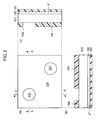
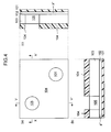
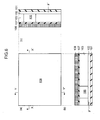
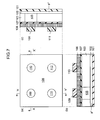
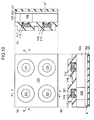
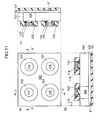
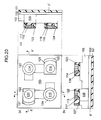
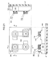
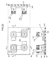
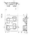
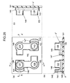
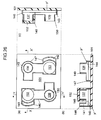
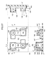
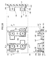
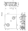
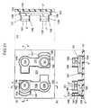
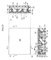
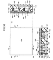
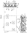
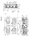
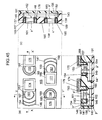
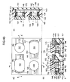
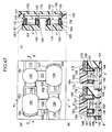
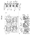
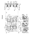
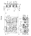
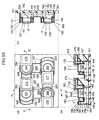
- FIG. 2 to FIG. 65 shows a step in the example of the production process, wherein the figure suffixed with (a), the figure suffixed with (b) and the figure suffixed with (c) are a top plan view, a sectional view taken along the line X-X' in the figure suffixed with (a), and a sectional view taken along the line Y-Y' in the figure suffixed with (a), respectively.
- (a) are top plan views in which some part is hatched for distinguishing regions.
- boron (B) is implanted into a p-type or non-doped silicon layer 103 formed on an oxide layer 101 to form a p+-type silicon layer 102 therein.
- a resist 104 for forming an n-type silicon layer is formed. In cases where after-mentioned silicon layers 105, 106 are formed as a non-doped type, this step is unnecessary.
- two n-type silicon layers 105, 106 are formed by implantation of phosphorus (P). In cases where these silicon layers 105, 106 are formed as a non-doped type, this step is unnecessary.
- the resist 104 is stripped away, and then a heat treatment is performed. In cases where the silicon layers 1.05, 106 are formed as a non-doped type, this step is unnecessary.
- an oxide film 107 is deposited, and then a nitride film 108 is deposited.
- four resists 109, 110, 111, 112 for forming four (first, second, third, and fourth) island-shaped silicon layers is formed.
- the nitride film 108 and the oxide film 107 are etched to form four nitride films 113, 114, 115 (one of the nitride films is indicated by the reference numeral 116 in FIG. 9 , etc.) and four oxide films 117, 118, 119 (one of the oxide films is not indicated by a reference numeral).
- the resists 109, 110, 111, 112 are stripped away.
- an oxide film 121 is deposited.
- the oxide film 121 is etched to form four oxide film-based sidewalls 122, 123, 124, 125.
- a nitride film 126 is deposited.
- the nitride film 126 is etched to form four nitride film-based sidewalls 127, 128, 129, 130.
- the nitride film-based sidewalls 127, 128, 129, 130 are etched to form two nitride film-based hard masks 127 (one of the nitride film-based hard masks is indicated by the reference numeral 130 in FIG. 17 , etc.) for forming first and second arc-shaped silicon layers.
- the oxide film-based sidewalls 122, 123, 124, 125 are etched.
- the resists 131, 132, 133, 134 are stripped away.
- two resists 135, 136 for forming a diffusion-layer interconnection section is formed.
- the silicon layer 103 is etched to form a diffusion-layer interconnection section thereon.
- the resists 135, 136 are stripped away.
- the oxide film-based sidewalls 122, 123, 124, 125 are etched away.
- the silicon layer 103 and silicon layers 105, 106 are etched to form a first island-shaped silicon layer 137, a third island-shaped silicon layer 138, a fourth island-shaped silicon layer 139, a second island-shaped silicon layer (indicated by the reference numeral 140 in FIG 23 , etc), a first arc-shaped silicon layer 141, a second arc-shaped silicon layer (indicated by the reference numeral 142 in FIG. 23 , etc), and fifth and sixth p+-type silicon layers 143, 144.
- the nitride films 113, 114, 115, 116 and the oxide films 117, 118, 119 are stripped away.
- a nitride film 145 is deposited.
- the nitride film 145 is etched to form six nitride film-based sidewalls 146, 147, 148, 149, 150, 151 for protecting channel regions during ion implantation in a subsequent step.
- two resists 152, 153 for forming an n+-type silicon layer are formed.
- arsenic (As) is implanted to form a first n+-type silicon layer 154, a second n+-type silicon layer 156, a third n+-type silicon layer 159, a fourth n+-type silicon layer 157, a fifth n+-type silicon layer 155, a sixth n+-type silicon layer 157, a seventh n+-type silicon layer 158 and an eighth n+-type silicon layer 156.
- the resists 152, 153 are stripped away.
- a resist 160 for forming a p+-type silicon layer is formed.
- boron (B) is implanted to form a first p+-type silicon layer 161, a second p+-type silicon layer 162, a third p+-type silicon layer 163 and a fourth p+-type silicon layer 164.
- the resist 160 is stripped away, and then a heat treatment is performed.
- an oxide film 165 is deposited, and then subjected to flattening and etching-back to expose the first n+-type silicon layer 154, the third n+-type silicon layer 159, the fifth n+-type silicon layer 155, the seventh n+-type silicon layer 158, the first p+-type silicon layer 161 and the third p+-type silicon layer 163.
- a resist 166 for forming a gate section is formed.
- a portion of the oxide film 165 corresponding to the gate section is etched.
- the resist 166 is stripped away.
- the nitride film-based sidewalls 148, 149, 150, 151 are etched away.
- a high-K (high-dielectric constant) film 167 is deposited, and then a metal 168, such as titanium nitride (TiN); is deposited.
- a metal 168 such as titanium nitride (TiN)
- a nitride film 169 is deposited.
- the nitride film 169 is etched to form four nitride film-based hard masks 174, 175 (two of the nitride film-based hard masks are indicated by the reference numerals 176, 177 in FIG. 41 , etc.)
- the resists 170, 171, 172, 173 are stripped away.
- the metal 168 is etched to form first to fourth gate electrodes 178, 181, 179, 180.
- a nitride film 182 is deposited.
- the nitride film 182 is etched to form four nitride film-based sidewalls 183, 184, 185, 186.
- the high-K film is etched to form first to six high-K films (gate dielectric films) 187, 187, 190, 190, 188, 189.
- high-K films gate dielectric films
- resists 191, 192, 193, 194 for etching the oxide film 165 is formed.
- the oxide film 165 is dry-etched.
- the resists 191, 192, 193, 194 are stripped away.
- the oxide film 165 is wet-etched.
- a nitride film 195 is deposited.
- the nitride film 195 is etched to form nitride film-based sidewalls 195.
- the oxide film 165 is dry-etched.
- the oxide film 165 is wet-etched to expose the nitride film-based sidewalls 146, 147.
- the nitride film-based sidewalls 195 are etched, and a part of the nitride film-based sidewalls 146, 147 is etched, to expose a part of respective sidewalls of the second n+-type silicon layer 156, the fifth p+-type silicon layer 143, and a part of respective sidewalls of the fourth n+-type silicon layer 157 and the sixth p+-type silicon layer 144.
- a metal such as nickel (Ni) or cobalt (Co) is deposited. Subsequently, a heat treatment is performed, and then an unreacted metal film is removed, to obtain a first silicon-metal compound layer 204 formed on a part of the sidewalls of the second n+-type silicon layer 156 and the fifth p+-type silicon layer 143, a second silicon-metal compound layer 201 formed on the eighth n+ silicon layer 156 and the fifth p+-type silicon layer 143, a third silicon-metal compound layer 205 formed on a part of the sidewalls of the fourth n+-type silicon layer 157 and the sixth p+-type silicon layer 144, a fourth silicon-metal compound layer 198 formed on the sixth n+-type silicon layer 157 and the sixth p+-type silicon layer 144; a fifth silicon-metal compound layer 197 formed on the first p+-type silicon layer 161, a sixth silicon-metal compound layer 196
- an interlayer film 206 such as an oxide film, is formed.
- a contact hole 207 is formed to expose a part of the first gate electrode 178 and the fourth silicon-metal compound layer 198, and a contact hole 208 is formed to expose a part of the second gate electrode 181 and the second silicon-metal compound layer 201.
- a metal such as tungsten (W) is deposited to form first and second contacts 209, 210.
- an interlayer film 211 is formed.
- a contact hole 212 is formed on the third gate electrode 179, and a contact hole 213 is formed on the fourth gate electrode 180.
- a contact hole 214 is formed on the sixth silicon-metal compound layer 196, and a contact hole 215 is formed on the eighth silicon-metal compound layer 203.
- four contact holes 216, 217, 218, 219 are formed on the fifth silicon-metal compound layer 197, the ninth silicon-metal compound layer 199, the tenth silicon-metal compound layer 200 and the seventh silicon-metal compound layer 202, respectively.
- a metal such as tungsten (W) is deposited to form eight contacts 220,221,222,223,224,225,226,227.
- first level metals 228, 229, 230, 231, 232, 233, 234, 235 are formed on respective ones of the eight contacts.
- an interlayer film 236 is formed. In the above manner, an SRAM memory cell is formed.
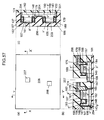
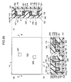
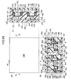
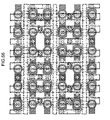
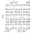
- FIG. 66 shows the semiconductor device structure formed by arranging the semiconductor device according to the above embodiment in a three-row by three-column array.
- FIG. 67 shows an inverter output terminal layer in the semiconductor device structure
- FIG. 68 shows a transistor layer in the semiconductor device structure
- FIG. 69 shows a contact layer and a first level metal layer in the semiconductor device structure
- FIG. 70 shows a second level metal layer, and a first level via (a contact between the first level metal layer and the second level metal layer), in the semiconductor device structure.
- FIG. 71 shows a third level metal layer, and a second level via (a contact between the second level metal layer and the third level metal layer), in the semiconductor device structure, and
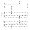
- FIG. 72 shows a fourth level metal layer, and a third level via (a contact between the third level metal layer and the fourth level metal layer), in the semiconductor device structure.
- An inverter 319 is arranged at an intersection of the 1st row and the 1st column.
- a selection transistor 337 is arranged at an intersection of the 1st row and the 2nd column.
- a selection transistor 340 is arranged at an intersection of the 2nd row and the 1st column.
- An inverter 322 is arranged at an intersection of the 2nd row and the 2nd column.
- the inverter 319 and the selection transistor 340 are connected to each other by an output terminal 301.
- the inverter 322 and the selection transistor 337 are connected to each other by an output terminal 302.
- An input terminal 355 of the inverter 319 is connected to the output terminal 302 via a contact 374.
- An input terminal 358 of the inverter 322 is connected to the output terminal 301 via a contact 373.
- An inverter 320 is arranged at an intersection of the 1st row and the 4th column.
- a selection transistor 338 is arranged at an intersection of the 1st row and the 3rd column.
- a selection transistor 341 is arranged at an intersection of the 2nd row and the 4th column.
- An inverter 323 is arranged at an intersection of the 2nd row and the 3rd column.
- the inverter 323 and the selection transistor 338 are connected to each other by an output terminal 303.
- the inverter 320 and the selection transistor 341 are connected to each other by an output terminal 304.
- An input terminal 359 of the inverter 323 is connected to the output terminal 304 via a contact 376.
- An input terminal 356 of the inverter 320 is connected to the output terminal 303 via a contact 375.
- An inverter 321 is arranged at an intersection of the 1st row and the 5th column.
- a selection transistor 339 is arranged at an intersection of the 1st row and the 6th column.
- a selection transistor 342 is arranged at an intersection of the 2nd row and the 5th column.
- An inverter 324 is arranged at an intersection of the 2nd row and the 6th column.
- the inverter 321 and the selection transistor 342 are connected to each other by an output terminal 305.
- the inverter 324 and the selection transistor 339 are connected to each other by an output terminal 306.
- An input terminal 357 of the inverter 321 is connected to the output terminal 306 via a contact 378.
- An input terminal 360 of the inverter 324 is connected to the output terminal 305 via a contact 377.
- the selection transistor 340 has a gate electrode 393.
- the selection transistor 337 and the selection transistor 338 have a gate electrode 391.
- the selection transistor 341 and the selection transistor 342 have a gate electrode 394.
- the selection transistor 339 has a gate electrode 392.
- An inverter 325 is arranged at an intersection of the 3rd row and the 2nd column.
- a selection transistor 343 is arranged at an intersection of the 3rd row and the 1st column.
- a selection transistor 346 is arranged at an intersection of the 4th row and the 2nd column.
- An inverter 328 is arranged at an intersection of the 4th row and the 1st column.
- the inverter 328 and the selection transistor 343 are connected to each other by an output terminal 307.
- the inverter 325 and the selection transistor 346 are connected to each other by an output terminal 308.
- An input terminal 364 of the inverter 328 is connected to the output terminal 308 via a contact 380.
- An input terminal 361 of the inverter 325 is connected to the output terminal 307 via a contact 379.
- An inverter 326 is arranged at an intersection of the 3rd row and the 3rd column.
- a selection transistor 344 is arranged at an intersection of the 3rd row and the 4th column.
- a selection transistor 347 is arranged at an intersection of the 4th row and the 3rd column.
- An inverter 329 is arranged at an intersection of the 4th row and the 4th column.
- the inverter 326 and the selection transistor 347 are connected to each other by an output terminal 309.
- the inverter 329 and the selection transistor 344 are connected to each other by an output terminal 310.
- An input terminal 362 of the inverter 326 is connected to the output terminal 310 via a contact 382.
- An input terminal 365 of the inverter 329 is connected to the output terminal 309 via a contact 381.
- An inverter 327 is arranged at an intersection of the 3rd row and the 6th column.
- a selection transistor 345 is arranged at an intersection of the 3rd row and the 5th column.
- a selection transistor 348 is arranged at an intersection of the 4th row and the 6th column.
- An inverter 330 is arranged at an intersection of the 4th row and the 5th column.
- the inverter 330 and the selection transistor 345 are connected to each other by an output terminal 311.
- the inverter 327 and the selection transistor 348 are connected to each other by an output terminal 312.
- An input terminal 366 of the inverter 330 is connected to the output terminal 312 via a contact 384.
- An input terminal 363 of the inverter 327 is connected to the output terminal 311 via a contact 383.
- the selection transistor 343 has a gate electrode 395.
- the selection transistor 346 and the selection transistor 347 have a gate electrode 397.
- the selection transistor 344 and the selection transistor 345 have a gate electrode 396.
- the selection transistor 348 has a gate electrode 398.
- An inverter 331 is arranged at an intersection of the 5th row and the 1st column.
- a selection transistor 349 is arranged at an intersection of the 5th row and the 2nd column.
- a selection transistor 352 is arranged at an intersection of the 6th row and the 1st column.
- An inverter 334 is arranged at an intersection of the 6th row and the 2nd column.
- the inverter 331 and the selection transistor 352 are connected to each other by an output terminal 313.
- the inverter 334 and the selection transistor 349 are connected to each other by an output terminal 314.
- An input terminal 367 of the inverter 331 is connected to the output terminal 314 via a contact 386.
- An input terminal 370 of the inverter 334 is connected to the output terminal 313 via a contact 385.
- An inverter 332 is arranged at an intersection of the 5th row and the 4th column.
- a selection transistor 350 is arranged at an intersection of the 5th row and the 3rd column.
- a selection transistor 353 is arranged at an intersection of the 6th row and the 4th column.
- An inverter 335 is arranged at an intersection of the 6th row and the 3rd column.
- the inverter 335 and the selection transistor 350 are connected to each other by an output terminal 315.
- the inverter 332 and the selection transistor 353 are connected to each other by an output terminal 316.
- An input terminal 371 of the inverter 335 is connected to the output terminal 316 via a contact 388.
- An input terminal 368 of the inverter 332 is connected to the output terminal 315 via a contact 387.
- An inverter 333 is arranged at an intersection of the 5th row and the 5th column.
- a selection transistor 351 is arranged at an intersection of the 5th row and the 6th column.
- a selection transistor 354 is arranged at an intersection of the 6th row and the 5th column.
- An inverter 336 is arranged at an intersection of the 6th row and the 6th column.
- the inverter 333 and the selection transistor 354 are connected to each other by an output terminal 317.
- the inverter 336 and the selection transistor 351 are connected to each other by an output terminal 318.
- An input terminal 369 of the inverter 333 is connected to the output terminal 318 via a contact 390.
- An input terminal 372 of the inverter 336 is connected to the output terminal 317 via a contact 389.
- the selection transistor 352 has a gate electrode 401.
- the selection transistor 349 and the selection transistor 350 have a gate electrode 399.
- the selection transistor 353 and the selection transistor 354 have a gate electrode 402.
- the selection transistor 351 has a gate electrode 400.
- a contact 403 is arranged on an nMOS transistor of the inverter 319, and a contact 404 is arranged on a pMOS transistor of the inverter 319.
- a contact 412 is arranged on the selection transistor 340.
- a contact 414 is arranged on an nMOS transistor of the inverter 322, and a contact 413 is arranged on a pMOS transistor of the inverter 322.
- a contact 405 is arranged on the selection transistor 337.
- the contact 414 is also arranged on an nMOS transistor of the inverter 323, and a contact 415 is arranged on a pMOS transistor of the inverter 323.
- a contact 407 is arranged on the selection transistor 338.
- a contact 409 is arranged on an nMOS transistor of the inverter 320, and a contact 408 is arranged on a pMOS transistor of the inverter 320.
- a contact 416 is arranged on the selection transistor 341.
- the contact 409 is also arranged on an nMOS transistor of the inverter 321, and a contact 410 is arranged on a pMOS transistor of the inverter 321.
- a contact 418 is arranged on the selection transistor 342.
- a contact 420 is arranged on an nMOS transistor of the inverter 324, and a contact 419 is arranged on a pMOS transistor of the inverter 324.
- a contact 411 is arranged on the selection transistor 339.
- a contact 406 is arranged on the gate electrode 391, and a contact 417 is arranged on the gate electrode 394.
- a contact 430 is arranged on an nMOS transistor of the inverter 328, and a contact 431 is arranged on a pMOS transistor of the inverter 328.
- a contact 421 is arranged on the selection transistor 343.
- a contact 423 is arranged on an nMOS transistor of the inverter 325, and a contact 422 is arranged on a pMOS transistor of the inverter 325.
- a contact 432 is arranged on the selection transistor 346.
- the contact 423 is also arranged on an nMOS transistor of the inverter 326, and a contact 424 is arranged on a pMOS transistor of the inverter 326.
- a contact 434 is arranged on the selection transistor 347.
- a contact 436 is arranged on an nMOS transistor of the inverter 329, and a contact 435 is arranged on a pMOS transistor of the inverter 329.
- a contact 425 is arranged on the selection transistor 344.
- the contact 436 is also arranged on an nMOS transistor of the inverter 330, and a contact 437 is arranged on a pMOS transistor of the inverter 330.
- a contact 427 is arranged on the selection transistor 345.
- a contact 429 is arranged on an nMOS transistor of the inverter 327, and a contact 428 is arranged on a pMOS transistor of the inverter 327.
- a contact 438 is arranged on the selection transistor 348.
- a contact 433 is arranged on the gate electrode 397, and a contact 426 is arranged on the gate electrode 396.
- a contact 439 is arranged on an nMOS transistor of the inverter 331, and a contact 440 is arranged on a pMOS transistor of the inverter 331.
- a contact 448 is arranged on the selection transistor 352.
- a contact 450 is arranged on an nMOS transistor of the inverter 334, and a contact 449 is arranged on a pMOS transistor of the inverter 334.
- a contact 441 is arranged on the selection transistor 349.
- the contact 450 is also arranged on an nMOS transistor of the inverter 335, and a contact 451 is arranged on a pMOS transistor of the inverter 335.
- a contact 443 is arranged on the selection transistor 350.
- a contact 445 is arranged on an nMOS transistor of the inverter 332, and a contact 444 is arranged on a pMOS transistor of the inverter 332.
- a contact 452 is arranged on the selection transistor 353.
- the contact 445 is also arranged on an nMOS transistor of the inverter 333, and a contact 446 is arranged on a pMOS transistor of the inverter 333.
- a contact 454 is arranged on the selection transistor 354.
- a contact 456 is arranged on an nMOS transistor of the inverter 336, and a contact 455 is arranged on a pMOS transistor of the inverter 336.
- a contact 447 is arranged on the selection transistor 351.
- a contact 442 is arranged on the gate electrode 399, and a contact 453 is arranged on the gate electrode 402.
- a first level metal 457 is connected to the contact 403, and a first level metal 458 is connected to the contact 404.
- a first level metal 459 is connected to the contact 405, and a first level metal 460 is connected to the contact 406.
- a first level metal 461 is connected to the contact 407, and a first level metal 462 is connected to the contact 408.
- a first level metal 463 is connected to the contact 409, and a first level metal 464 is connected to the contact 410.
- a first level metal 465 is connected to the contact 411.
- a first level metal 466 is connected to the contacts 412, 421, and a first level metal 467 is connected to the contacts 413, 422.
- a first level metal 468 is connected to the contacts 414, 423, and a first level metal 469 is connected to the contacts 415, 424.
- a first level metal 470 is connected to the contacts 416, 425.
- a first level metal 471 is connected to the contact 417, and a first level metal 472 is connected to the contact 472.
- a first level metal 473 is connected to the contacts 418, 427.
- a first level metal 474 is connected to the contacts 419, 428, and a first level metal 475 is connected to the contacts 420, 429.
- a first level metal 476 is connected to the contacts 430, 439, and a first level metal 477 is connected to the contacts 431, 440.
- a first level metal 478 is connected to the contacts 432, 441.
- a first level metal 479 is connected to the contact 433, and a first level metal 480 is connected to the contact 442.
- a first level metal 481 is connected to the contacts 434, 443.
- a first level metal 482 is connected to the contacts 435, 444, and a first level metal 483 is connected to the contacts 436, 445.
- a first level metal 484 is connected to the contacts 437, 446, and a first level metal 485 is connected to the contacts 438, 447.
- a first level metal 486 is connected to the contact 448, and a first level metal 487 is connected to the contact 449.
- a first level metal 488 is connected to the contact 450, and a first level metal 489 is connected to the contact 451.
- a first level metal 490 is connected to the contact 452, and a first level metal 491 is connected to the contact 453.
- a first level metal 492 is connected to the contact 454, and a first level metal 493 is connected to the contact 455.
- a first level metal 494 is connected to the contact 456.
- a first level via 495 is arranged on the first level metal 460, and a first level via 496 is arranged on the first level metal 471.
- a first level via 497 is arranged on the first level metal 466, and a first level via 498 is arranged on the first level metal 467.
- a first level via 499 is arranged on the first level metal 468, and a first level via 500 is arranged on the first level metal 469.
- a first level via 501 is arranged on the first level metal 470, and a first level via 502 is arranged on the first level metal 473.
- a first level via 503 is arranged on the first level metal 474.
- a first level via 505 is arranged on the first level metal 479, and a first level via 504 is arranged on the first level metal 472.
- a first level via 506 is arranged on the first level metal 477, and a first level via 507 is arranged on the first level metal 478.
- a first level via 508 is arranged on the first level metal 481, and a first level via 509 is arranged on the first level metal 482.
- a first level via 510 is arranged on the first level metal 483, and a first level via 511 is arranged on the first level metal 484.
- a first level via 512 is arranged on the first level metal 485.
- a first level via 513 is arranged on the first level metal 480, and a first level via 514 is arranged on the first level metal 491.
- a second level metal 515 is connected to the first level vias 495, 496.
- a second level metal 516 is connected to the first level via 497, and a second level metal 517 is connected to the first level via 498.
- a second level metal 518 is connected to the first level via 499, and a second level metal 519 is connected to the first level via 500.
- a second level metal 520 is connected to the first level via 501, and a second level metal 521 is connected to the first level via 502.
- a second level metal 522 is connected to the first level via 503.
- a second level metal 523 is connected to the first level vias 505, 504.
- a second level metal 523 is connected to the first level via 506, and a second level metal 525 is connected to the first level via 507.
- a second level metal 526 is connected to the first level via 508, and a second level metal 527 is connected to the first level via 509.
- a second level metal 528 is connected to the first level via 510, and a second level metal 529 is connected to the first level via 511.
- a second level metal 530 is connected to the first level via 512.
- a second level metal 531 is connected to the first level vias 513, 514.
- a second level via 532 is arranged on the second level metal 516, and a second level via 533 is arranged on the second level metal 517.
- a second level via 534 is arranged on the second level metal 518, and a second level via 535 is arranged on the second level metal 519.
- a second level via 536 is arranged on the second level metal 520, and a second level via 537 is arranged on the second level metal 521.
- a second level via 538 is arranged on the second level metal 522, and a second level via 539 is arranged on the second level metal 524.
- a second level via 540 is arranged on the second level metal 525, and a second level via 541 is arranged on the second level metal 526.
- a second level via 542 is arranged on the second level metal 527, and a second level via 543 is arranged on the second level metal 528.
- a second level via 544 is arranged on the second level metal 529, and a second level via 545 is arranged on the second level metal 530.
- a third level metal 546 is connected to the second level via 534, and a third level metal 549 is connected to the second level via 532.
- a third level metal 550 is connected to the second level via 536, and a third level metal 551 is connected to the second level via 537.
- a third level metal 547 is connected to the second level vias 533, 535, 538, 539, 542, 544.
- a third level metal 552 is connected to the second level via 540, and a third level metal 553 is connected to the second level via 541.
- a third level metal 554 is connected to the second level via 545, and a third level metal 548 is connected to the second level via 543.
- a third level via 561 is arranged on the third level metal 549, and a third level via 564 is arranged on the third level metal 550.
- a third level via 565 is arranged on the third level meta! 551, and a third level via 562 is arranged on the third level metal 552.
- a third level via 563 is arranged on the third level metal 553, and a third level via 566 is arranged on the third level metal 554.
- a fourth level metal 555 is connected to the third level via 561, and a fourth level metal 556 is connected to the third level via 562.
- a fourth level metal 557 is connected to the third level via 563, and a fourth level metal 558 is connected to the third level via 564.
- a fourth level metal 559 is connected to the third level via 565, and a fourth level metal 560 is connected to the third level via 566.
Landscapes
- Metal-Oxide And Bipolar Metal-Oxide Semiconductor Integrated Circuits (AREA)
- Thin Film Transistor (AREA)
- Semiconductor Memories (AREA)
Abstract
Description
- The present invention relates to a semiconductor device.
- A degree of integration in a semiconductor device, particularly in an integrated circuit using a MOS transistor, has been increasing year by year. Along with the increase in the degree of integration, miniaturization of the MOS transistor used therein has progressed to a nano region. The progress in miniaturization of the MOS transistor, which constitutes an inverter circuit as a basic circuit for digital circuits, gives rise to a problem, such as difficulty in suppressing a leak current, which causes deterioration in reliability due to hot carrier effects and poses an impediment to sufficiently reducing a circuit occupancy area while meeting a requirement of ensuring a necessary current magnitude. With a view to solving this problem, there have been proposed a surrounding gate transistor (SGT) having a structure in which a source, a gate and a drain are arranged in a direction perpendicular to a substrate, wherein the gate is formed to surround an island-shaped semiconductor layer, and a CMOS inverter circuit using the SGT (see, for example, S. Watanabe, K. Tsuchida, D. Takashima, Y Oowaki, A. Nitayama, K. Hieda, H. Takato, K. Sunouchi, F. Horiguchi, K. Ohuchi, F. Masuoka, H. Hara, "A Novel Circuit Technology with Surrounding Gate Transistors (SGT's) for Ultra High Density DRAM's," IEEE JSSC, Vol. 30, No. 9, 1995).
- An inverter is constructed using a pMOS transistor and an nMOS transistor. In an inverter circuit, a gate width of a pMOS transistor has to be set to be twice as large as that of an nMOS transistor, because a hole mobility is one-half of an electron mobility. Therefore, a conventional CMOS inverter circuit using an SGT (SGT CMOS inverter circuit) is composed of two pMOS SGTs and one nMOS SGT. In other words, the conventional SGT CMOS inverter circuit is composed of total three island-shaped semiconductors.
- An SRAM is composed of two inverters and two selection transistors. In cases where an SRAM is constructed using the conventional SGT CMOS inverter circuit, it is composed of four pMOS and four nMOS. In other words, the SRAM using the conventional SGT CMOS inverter circuit is composed of total eight island-shaped semiconductors.
- It is therefore an object of the present invention to provide a semiconductor device comprising a highly-integrated SGT-based SRAM.
- In order to achieve this object, according to a first aspect of the present invention, there is provided a semiconductor device which is characterized by comprising: a first inverter arranged at an intersection of the 1 st row and the 1st column, wherein the first inverter includes a first island-shaped semiconductor layer, a first gate dielectric film in contact with at least a part of a periphery of the first island-shaped semiconductor layer, a first gate electrode having one surface in contact with the first gate dielectric film, a second gate dielectric film in contact with another surface of the first gate electrode, a first arc-shaped semiconductor layer in contact with at least a part of the second gate dielectric film, a first first-conductive-type high-concentration semiconductor layer arranged on a top of the first island-shaped semiconductor layer, a second first-conductive-type high-concentration semiconductor layer arranged underneath the first island-shaped semiconductor layer, a first second-conductive-type high-concentration semiconductor layer arranged on a top of the first arc-shaped semiconductor layer, and a second second-conductive-type high-concentration semiconductor layer arranged underneath the first arc-shaped semiconductor layer; a second inverter arranged at an intersection of the 2nd row and the 2nd column, wherein the second inverter includes a second island-shaped semiconductor layer, a third gate dielectric film in contact with at least a part of a periphery of the second island-shaped semiconductor layer, a second gate electrode having one surface in contact with the third gate dielectric film, a fourth gate dielectric film in contact with another surface of the second gate electrode, a second arc-shaped semiconductor layer in contact with at least a part of the fourth gate dielectric film, a third first-conductive-type high-concentration semiconductor layer arranged on a top of the second island-shaped semiconductor layer, a fourth first-conductive-type high-concentration semiconductor layer arranged underneath the second island-shaped semiconductor layer, a third second-conductive-type high-concentration semiconductor layer arranged on a top of the second arc-shaped semiconductor layer, and a fourth second-conductive-type high-concentration semiconductor layer arranged underneath the second arc-shaped semiconductor layer; a first selection transistor arranged at an intersection of the 1st row and the 2nd column, wherein the first selection transistor includes a third island-shaped semiconductor layer, a fifth gate dielectric film in contact with at least a part of a periphery of the third island-shaped semiconductor layer, a third gate electrode partially in contact with the fifth gate dielectric film, a fifth second-conductive-type high-concentration semiconductor layer arranged on a top of the third island-shaped semiconductor layer, and a sixth second-conductive-type high-concentration semiconductor layer arranged underneath the third island-shaped semiconductor layer; and a second selection transistor arranged at an intersection of the 2nd row and the 1 st column, wherein the second selection transistor includes a fourth island-shaped semiconductor layer, a sixth gate dielectric film in contact with at least a part of a periphery of the fourth island-shaped semiconductor layer, a fourth gate electrode partially in contact with the sixth gate dielectric film, a seventh second-conductive-type high-concentration semiconductor layer arranged on a top of the fourth island-shaped semiconductor layer, and an eighth second-conductive-type high-concentration semiconductor layer arranged underneath the fourth island-shaped semiconductor layer.
- According to a second aspect of the present invention, there is provided a semiconductor device which is characterized by comprising: a first inverter arranged at an intersection of the 1st row and the 1st column, wherein the first inverter includes a first island-shaped semiconductor layer, a first gate dielectric film surrounding a periphery of the first island-shaped semiconductor layer, a first gate electrode surrounding a periphery of the first gate dielectric film, a second gate dielectric film surrounding a part of a periphery of the first gate electrode, a first arc-shaped semiconductor layer in contact with a part of a periphery of the second gate dielectric film, a first first-conductive-type high-concentration semiconductor layer arranged on a top of the first island-shaped semiconductor layer, a second first-conductive-type high-concentration semiconductor layer arranged underneath the first island-shaped semiconductor layer, a first second-conductive-type high-concentration semiconductor layer arranged on a top of the first arc-shaped semiconductor layer, and a second second-conductive-type high-concentration semiconductor layer arranged underneath the first arc-shaped semiconductor layer; a second inverter arranged at an intersection of the 2nd row and the 2nd column, wherein the second inverter includes a second island-shaped semiconductor layer, a third gate dielectric film surrounding a periphery of the second island-shaped semiconductor layer, a second gate electrode surrounding a periphery of the third gate dielectric film, a fourth gate dielectric film surrounding a part of a periphery of the second gate electrode, a second arc-shaped semiconductor layer in contact with a part of a periphery of the fourth gate dielectric film, a third first-conductive-type high-concentration semiconductor layer arranged on a top of the second island-shaped semiconductor layer, a fourth first-conductive-type high-concentration semiconductor layer arranged underneath the second island-shaped semiconductor layer, a third second-conductive-type high-concentration semiconductor layer arranged on a top of the second arc-shaped semiconductor layer, and a fourth second-conductive-type high-concentration semiconductor layer arranged underneath the second arc-shaped semiconductor layer; a first selection transistor arranged at an intersection of the 1st row and the 2nd column, wherein the first selection transistor includes a third island-shaped semiconductor layer, a fifth gate dielectric film surrounding a periphery of the third island-shaped semiconductor layer, a third gate electrode surrounding a periphery of the fifth gate dielectric film, a fifth second-conductive-type high-concentration semiconductor layer arranged on a top of the third island-shaped semiconductor layer, and a sixth second-conductive-type high-concentration semiconductor layer arranged underneath the third island-shaped semiconductor layer; and a second selection transistor arranged at an intersection of the 2nd row and the 1st column, wherein the second selection transistor includes a fourth island-shaped semiconductor layer, a sixth gate dielectric film surrounding a periphery of the fourth island-shaped semiconductor layer, a fourth gate electrode surrounding a periphery of the sixth gate dielectric film, a seventh second-conductive-type high-concentration semiconductor layer arranged on a top of the fourth island-shaped semiconductor layer, and an eighth second-conductive-type high-concentration semiconductor layer arranged underneath the fourth island-shaped semiconductor layer.
- According to a third aspect of the present invention, there is provided a semiconductor device which is characterized by comprising: a first inverter arranged at an intersection of the 1st row and the 1st column, wherein the first inverter includes a first island-shaped semiconductor layer, a first gate dielectric film surrounding a periphery of the first island-shaped semiconductor layer, a first gate electrode surrounding a periphery of the first gate dielectric film, a second gate dielectric film surrounding a part of a periphery of the first gate electrode, a first arc-shaped semiconductor layer in contact with a part of a periphery of the second gate dielectric film, a first first-conductive-type high-concentration semiconductor layer arranged on a top of the first island-shaped semiconductor layer, a second first-conductive-type high-concentration semiconductor layer arranged underneath the first island-shaped semiconductor layer, a first second-conductive-type high-concentration semiconductor layer arranged on a top of the first arc-shaped semiconductor layer, and a second second-conductive-type high-concentration semiconductor layer arranged underneath the first arc-shaped semiconductor layer; a second inverter arranged at an intersection of the 2nd row and the 2nd column, wherein the second inverter includes a second island-shaped semiconductor layer, a third gate dielectric film surrounding a periphery of the second island-shaped semiconductor layer, a second gate electrode surrounding a periphery of the third gate dielectric film, a fourth gate dielectric film surrounding a part of a periphery of the second gate electrode, a second arc-shaped semiconductor layer in contact with a part of a periphery of the fourth gate dielectric film, a third first-conductive-type high-concentration semiconductor layer arranged on a top of the second island-shaped semiconductor layer, a fourth first-conductive-type high-concentration semiconductor layer arranged underneath the second island-shaped semiconductor layer, a third second-conductive-type high-concentration semiconductor layer arranged on a top of the second arc-shaped semiconductor layer, and a fourth second-conductive-type high-concentration semiconductor layer arranged underneath the second arc-shaped semiconductor layer; a first selection transistor arranged at an intersection of the 1 st row and the 2nd column, wherein the first selection transistor includes a third island-shaped semiconductor layer, a fifth gate dielectric film surrounding a periphery of the third island-shaped semiconductor layer, a third gate electrode surrounding a periphery of the fifth gate dielectric film, a fifth second-conductive-type high-concentration semiconductor layer arranged on a top of the third island-shaped semiconductor layer, and a sixth second-conductive-type high-concentration semiconductor layer arranged underneath the third island-shaped semiconductor layer; a second selection transistor arranged at an intersection of the 2nd row and the 1st column, wherein the second selection transistor includes a fourth island-shaped semiconductor layer, a sixth gate dielectric film surrounding a periphery of the fourth island-shaped semiconductor layer, a fourth gate electrode surrounding a periphery of the sixth gate dielectric film, a seventh second-conductive-type high-concentration semiconductor layer arranged on a top of the fourth island-shaped semiconductor layer, and an eighth second-conductive-type high-concentration semiconductor layer arranged underneath the fourth island-shaped semiconductor layer; a fifth first-conductive-type high-concentration semiconductor layer arranged underneath the second first-conductive-type high-concentration semiconductor layer, the second second-conductive-type high-concentration semiconductor layer and the eighth second-conductive-type high-concentration semiconductor layer; a sixth first-conductive-type high-concentration semiconductor layer arranged underneath the fourth first-conductive-type high-concentration semiconductor layer, the fourth second-conductive-type high-concentration semiconductor layer and the sixth second-conductive-type high-concentration semiconductor layer; a first semiconductor-metal compound layer formed on a part of respective sidewalls of the second second-conductive-type high-concentration semiconductor layer and the fifth first-conductive-type high-concentration semiconductor layer; a second semiconductor-metal compound layer formed on the eighth second-conductive-type high-concentration semiconductor layer and the fifth first-conductive-type high-concentration semiconductor layer; a third semiconductor-metal compound layer formed on a part of respective sidewalls of the fourth second-conductive-type high-concentration semiconductor layer and the sixth first-conductive-type high-concentration semiconductor layer; a fourth semiconductor-metal compound layer formed on the sixth second-conductive-type high-concentration semiconductor layer and the sixth first-conductive-type high-concentration semiconductor layer; a fifth semiconductor-metal compound layer formed on the first first-conductive-type high-concentration semiconductor layer; a sixth semiconductor-metal compound layer formed on the first second-conductive-type high-concentration semiconductor layer; a seventh semiconductor-metal compound layer formed on the third first-conductive-type high-concentration semiconductor layer; an eighth semiconductor-metal compound layer formed on the third second-conductive-type high-concentration semiconductor layer; a ninth semiconductor-metal compound layer formed on the fifth second-conductive-type high-concentration semiconductor layer; a tenth semiconductor-metal compound layer formed on the seventh second-conductive-type high-concentration semiconductor layer; a first contact connecting the first gate electrode and the fourth semiconductor-metal compound layer; and a second contact connecting the second gate electrode and the second semiconductor-metal compound layer.
- According to a fourth aspect of the present invention, there is provided a semiconductor device which comprises: a first inverter arranged at an intersection of the 1st row and the 1 st column, wherein the first inverter includes a first island-shaped semiconductor layer, a first gate dielectric film surrounding a periphery of the first island-shaped semiconductor layer, a first gate electrode surrounding a periphery of the first gate dielectric film, a second gate dielectric film surrounding a part of a periphery of the first gate electrode, a first arc-shaped semiconductor layer in contact with a part of a periphery of the second gate dielectric film, a first p+-type semiconductor layer arranged on a top of the first island-shaped semiconductor layer, a second p+-type semiconductor layer arranged underneath the first island-shaped semiconductor layer, a first n+-type semiconductor layer arranged on a top of the first arc-shaped semiconductor layer and a second n+-type semiconductor layer arranged underneath the first arc-shaped semiconductor layer; a second inverter arranged at an intersection of the 2nd row and the 2nd column, wherein the second inverter includes a second island-shaped semiconductor layer, a third gate dielectric film surrounding a periphery of the second island-shaped semiconductor layer, a second gate electrode surrounding a periphery of the third gate dielectric film, a fourth gate dielectric film surrounding a part of a periphery of the second gate electrode, a second arc-shaped semiconductor layer in contact with a part of a periphery of the fourth gate dielectric film, a third p+-type semiconductor layer arranged on a top of the second island-shaped semiconductor layer, a fourth p+-type semiconductor layer arranged underneath the second island-shaped semiconductor layer, a third n+-type semiconductor layer arranged on a top of the second arc-shaped semiconductor layer, and a fourth n+-type semiconductor layer arranged underneath the second arc-shaped semiconductor layer; a first selection transistor arranged at an intersection of the 1st row and the 2nd column, wherein the first selection transistor includes a third island-shaped semiconductor layer, a fifth gate dielectric film surrounding a periphery of the third island-shaped semiconductor layer, a third gate electrode surrounding a periphery of the fifth gate dielectric film, a fifth n+-type semiconductor layer arranged on a top of the third island-shaped semiconductor layer, and a sixth n+-type semiconductor layer arranged underneath the third island-shaped semiconductor layer; and a second selection transistor arranged at an intersection of the 2nd row and the 1st column, wherein the second selection transistor includes a fourth island-shaped semiconductor layer, a sixth gate dielectric film surrounding a periphery of the fourth island-shaped semiconductor layer, a fourth gate electrode surrounding a periphery of the sixth gate dielectric film, a seventh n+-type semiconductor layer arranged on a top of the fourth island-shaped semiconductor layer, and an eighth n+-type semiconductor layer arranged underneath the fourth island-shaped semiconductor layer.
- According to a fifth aspect of the present invention, there is provided a semiconductor device which comprises: a first inverter arranged at an intersection of the 1st row and the 1st column, wherein the first inverter includes a first island-shaped semiconductor layer, a first gate dielectric film surrounding a periphery of the first island-shaped semiconductor layer, a first gate electrode surrounding a periphery of the first gate dielectric film, a second gate dielectric film surrounding a part of a periphery of the first gate electrode, a first arc-shaped semiconductor layer in contact with a part of a periphery of the second gate dielectric film, a first p+-type semiconductor layer arranged on a top of the first island-shaped semiconductor layer, a second p+-type semiconductor layer arranged underneath the first island-shaped semiconductor layer, a first n+-type semiconductor layer arranged on a top of the first arc-shaped semiconductor layer and a second n+-type semiconductor layer arranged underneath the first arc-shaped semiconductor layer; a second inverter arranged at an intersection of the 2nd row and the 2nd column, wherein the second inverter includes a second island-shaped semiconductor layer, a third gate dielectric film surrounding a periphery of the second island-shaped semiconductor layer, a second gate electrode surrounding a periphery of the third gate dielectric film, a fourth gate dielectric film surrounding a part of a periphery of the second gate electrode, a second arc-shaped semiconductor layer in contact with a part of a periphery of the fourth gate dielectric film, a third p+-type semiconductor layer arranged on a top of the second island-shaped semiconductor layer, a fourth p+-type semiconductor layer arranged underneath the second island-shaped semiconductor layer, a third n+-type semiconductor layer arranged on a top of the second arc-shaped semiconductor layer, and a fourth n+-type semiconductor layer arranged underneath the second arc-shaped semiconductor layer; a first selection transistor arranged at an intersection of the 1st row and the 2nd column, wherein the first selection transistor includes a third island-shaped semiconductor layer, a fifth gate dielectric film surrounding a periphery of the third island-shaped semiconductor layer, a third gate electrode surrounding a periphery of the fifth gate dielectric film, a fifth n+-type semiconductor layer arranged on a top of the third island-shaped semiconductor layer, and a sixth n+-type semiconductor layer arranged underneath the third island-shaped semiconductor layer; a second selection transistor arranged at an intersection of the 2nd row and the 1 st column, wherein the second selection transistor includes a fourth island-shaped semiconductor layer, a sixth gate dielectric film surrounding a periphery of the fourth island-shaped semiconductor layer, a fourth gate electrode surrounding a periphery of the sixth gate dielectric film, a seventh n+-type semiconductor layer arranged on a top of the fourth island-shaped semiconductor layer, and an eighth n+-type semiconductor layer arranged underneath the fourth island-shaped semiconductor layer; a fifth p+-type semiconductor layer arranged underneath the second p+-type semiconductor layer, the second n+-type semiconductor layer and the eighth n+-type semiconductor layer; a sixth p+-type semiconductor layer arranged underneath the fourth p+-type semiconductor layer, the fourth n+-type semiconductor layer and the sixth n+-type semiconductor layer; a first semiconductor-metal compound layer formed on a part of respective sidewalls of the second n+-type semiconductor layer and the fifth p+-type semiconductor layer; a second semiconductor-metal compound layer formed on the eighth n+-type semiconductor layer and the fifth p+-type semiconductor layer; a third semiconductor-metal compound layer formed on a part of respective sidewalls of the fourth n+-type semiconductor layer and the sixth p+-type semiconductor layer; a fourth semiconductor-metal compound layer formed on the sixth n+-type semiconductor layer and the sixth p+-type semiconductor layer; a fifth semiconductor-metal compound layer formed on the first p+-type semiconductor layer; a sixth semiconductor-metai compound layer formed on the first n+-type semiconductor layer; a seventh semiconductor-metal compound layer formed on the third p+-type semiconductor layer; an eighth semiconductor-metal compound layer formed on the third n+-type semiconductor layer; a ninth semiconductor-metal compound layer formed on the fifth n+-type semiconductor layer; a tenth semiconductor-metal compound layer formed on the seventh n+-type semiconductor layer; a first contact connecting the first gate electrode and the fourth semiconductor-metal compound layer; and a second contact connecting the second gate electrode and the second semiconductor-metal compound layer.
- Preferably, the semiconductor device of the present invention is configured to satisfy the following condition: Wp1 ≈ 2Wn1, wherein Wp1 is an outer peripheral length of the first island-shaped semiconductor layer, and Wn1 is a length of an arc of the first arc-shaped semiconductor layer in contact with a part of the periphery of the second gate dielectric film.
- Preferably, the semiconductor device of the present invention is configured to satisfy the following condition: Wp2 ≈ 2Wn2, wherein Wp2 is an outer peripheral length of the second island-shaped semiconductor layer, and Wn2 is a length of an arc of the second arc-shaped semiconductor layer in contact with a part of the periphery of the fourth gate dielectric film.
- Preferably, the semiconductor device of the present invention is configured to satisfy the following condition: Ln1 ≈ Lp1, wherein Ln1 is a channel length of the first arc-shaped semiconductor layer, and Lp1 is a channel length of the first island-shaped semiconductor layer.
- Preferably, the semiconductor device of the present invention is configured to satisfy the following condition: Ln2 ≈ Lp2, wherein Ln2 is a channel length of the second arc-shaped semiconductor layer, and Lp2 is a channel length of the second island-shaped semiconductor layer.
- Preferably, in the semiconductor device of the present invention, a first pMOS transistor, a first nMOS transistor, a second pMOS transistor and a second nMOS transistor are made up of a combination of the first island-shaped semiconductor layer, the first gate dielectric film surrounding the periphery of the first island-shaped semiconductor layer, the first gate electrode surrounding the periphery of the first gate dielectric film, the first p+-type semiconductor layer arranged on the top of the first island-shaped semiconductor layer, and the second p+-type semiconductor layer arranged underneath the first island-shaped semiconductor layer, a combination of the first gate electrode, the second gate dielectric film surrounding a part of the periphery of the first gate electrode, the first arc-shaped semiconductor layer in contact with a part of a periphery of the second gate dielectric film, a first n+-type semiconductor layer arranged on the top of the first arc-shaped semiconductor layer, and the second n+-type semiconductor layer arranged underneath the first arc-shaped semiconductor layer, a combination of the second island-shaped semiconductor layer, the third gate dielectric film surrounding the periphery of the second island-shaped semiconductor layer, the second gate electrode surrounding the periphery of the third gate dielectric film, the third p+-type semiconductor layer arranged on the top of the second island-shaped semiconductor layer, and the fourth p+-type semiconductor layer arranged underneath the second island-shaped semiconductor layer, and a combination of the second gate electrode, the fourth gate dielectric film surrounding a part of the periphery of the second gate electrode, the second arc-shaped semiconductor layer in contact with a part of the periphery of the fourth gate dielectric film, the third n+-type semiconductor layer arranged on the top of the second arc-shaped semiconductor layer, and the fourth n+-type semiconductor layer arranged underneath the second arc-shaped semiconductor layer, respectively, wherein: the first gate dielectric film is adapted to allow the first pMOS transistor to operate as an enhancement type; the second gate dielectric film is adapted to allow the first nMOS transistor to operate as an enhancement type; the first electrode is made of a material allowing the first pMOS transistor and the first nMOS transistor to operate as an enhancement type; the third gate dielectric film is adapted to allow the second nMOS transistor to operate as an enhancement type, and the first electrode is made of a material allowing the second pMOS transistor and the second nMOS transistor to operate as an enhancement type.
- Preferably, in the semiconductor device according to the fifth aspect of the present invention, each of the first to tenth semiconductor-metal compound layers is a silicon-metal compound layer.
- In the semiconductor device of the present invention, the first island-shaped semiconductor layer, the first arc-shaped semiconductor layer, the second island-shaped semiconductor layer, the second arc-shaped semiconductor layer, the third island-shaped semiconductor layer and the fourth island-shaped semiconductor layer may be a first island-shaped silicon layer, a first arc-shaped silicon layer, a second island-shaped silicon layer, a second arc-shaped silicon layer, a third island-shaped silicon layer and a fourth island-shaped silicon layer, respectively. Further, each of the n+-type semiconductor layers may be a p+-type silicon layer, and each of the p+-type semiconductor layers may be a p+-type silicon layer.
- Preferably, in the above semiconductor device, the first island-shaped silicon layer, the first arc-shaped silicon layer, the second island-shaped silicon layer, the second arc-shaped silicon layer, the third island-shaped silicon layer and the fourth island-shaped silicon layer are a first n-type or non-doped island-shaped silicon layer, a first p-type or non-doped arc-shaped silicon layer, a second n-type or non-doped island-shaped silicon layer, a second p-type or non-doped arc-shaped silicon layer, a third p-type or non-doped island-shaped silicon layer and a fourth p-type or non-doped island-shaped silicon layer, respectively.
- As above, the semiconductor device according to the first aspect of the present invention comprises: a first inverter arranged at an intersection of the 1st row and the 1st column, wherein the first inverter includes a first island-shaped semiconductor layer, a first gate dielectric film in contact with at least a part of a periphery of the first island-shaped semiconductor layer, a first gate electrode having one surface in contact with the first gate dielectric film, a second gate dielectric film in contact with another surface of the first gate electrode, a first arc-shaped semiconductor layer in contact with at least a part of the second gate dielectric film, a first first-conductive-type high-concentration semiconductor layer arranged on a top of the first island-shaped semiconductor layer, a second first-conductive-type high-concentration semiconductor layer arranged underneath the first island-shaped semiconductor layer, a first second-conductive-type high-concentration semiconductor layer arranged on a top of the first arc-shaped semiconductor layer, and a second second-conductive-type high-concentration semiconductor layer arranged underneath the first arc-shaped semiconductor layer; a second inverter arranged at an intersection of the 2nd row and the 2nd column, wherein the second inverter includes a second island-shaped semiconductor layer, a third gate dielectric film in contact with at least a part of a periphery of the second island-shaped semiconductor layer, a second gate electrode having one surface in contact with the third gate dielectric film, a fourth gate dielectric film in contact with another surface of the second gate electrode, a second arc-shaped semiconductor layer in contact with at least a part of the fourth gate dielectric film, a third first-conductive-type high-concentration semiconductor layer arranged on a top of the second island-shaped semiconductor layer, a fourth first-conductive-type high-concentration semiconductor layer arranged underneath the second island-shaped semiconductor layer, a third second-conductive-type high-concentration semiconductor layer arranged on a top of the second arc-shaped semiconductor layer, and a fourth second-conductive-type high-concentration semiconductor layer arranged underneath the second arc-shaped semiconductor layer; a first selection transistor arranged at an intersection of the 1st row and the 2nd column, wherein the first selection transistor includes a third island-shaped semiconductor layer, a fifth gate dielectric film in contact with at least a part of a periphery of the third island-shaped semiconductor layer, a third gate electrode partially in contact with the fifth gate dielectric film, a fifth second-conductive-type high-concentration semiconductor layer arranged on a top of the third island-shaped semiconductor layer, and a sixth second-conductive-type high-concentration semiconductor layer arranged underneath the third island-shaped semiconductor layer; and a second selection transistor arranged at an intersection of the 2nd row and the 1st column, wherein the second selection transistor includes a fourth island-shaped semiconductor layer, a sixth gate dielectric film in contact with at least a part of a periphery of the fourth island-shaped semiconductor layer, a fourth gate electrode partially in contact with the sixth gate dielectric film, a seventh second-conductive-type high-concentration semiconductor layer arranged on a top of the fourth island-shaped semiconductor layer, and an eighth second-conductive-type high-concentration semiconductor layer arranged underneath the fourth island-shaped semiconductor layer. This makes it possible to provide a semiconductor device comprising a highly-integrated SGT-based SRAM.
- The semiconductor device according to the second aspect of the present invention comprises: a first inverter arranged at an intersection of the 1st row and the 1st column, wherein the first inverter includes a first island-shaped semiconductor layer, a first gate dielectric film surrounding a periphery of the first island-shaped semiconductor layer, a first gate electrode surrounding a periphery of the first gate dielectric film, a second gate dielectric film surrounding a part of a periphery of the first gate electrode, a first arc-shaped semiconductor layer in contact with a part of a periphery of the second gate dielectric film, a first first-conductive-type high-concentration semiconductor layer arranged on a top of the first island-shaped semiconductor layer, a second first-conductive-type high-concentration semiconductor layer arranged underneath the first island-shaped semiconductor layer, a first second-conductive-type high-concentration semiconductor layer arranged on a top of the first arc-shaped semiconductor layer, and a second second-conductive-type high-concentration semiconductor layer arranged underneath the first arc-shaped semiconductor layer; a second inverter arranged at an intersection of the 2nd row and the 2nd column, wherein the second inverter includes a second island-shaped semiconductor layer, a third gate dielectric film surrounding a periphery of the second island-shaped semiconductor layer, a second gate electrode surrounding a periphery of the third gate dielectric film, a fourth gate dielectric film surrounding a part of a periphery of the second gate electrode, a second arc-shaped semiconductor layer in contact with a part of a periphery of the fourth gate dielectric film, a third first-conductive-type high-concentration semiconductor layer arranged on a top of the second island-shaped semiconductor layer, a fourth first-conductive-type high-concentration semiconductor layer arranged underneath the second island-shaped semiconductor layer, a third second-conductive-type high-concentration semiconductor layer arranged on a top of the second arc-shaped semiconductor layer, and a fourth second-conductive-type high-concentration semiconductor layer arranged underneath the second arc-shaped semiconductor layer; a first selection transistor arranged at an intersection of the 1st row and the 2nd column, wherein the first selection transistor includes a third island-shaped semiconductor layer, a fifth gate dielectric film surrounding a periphery of the third island-shaped semiconductor layer, a third gate electrode surrounding a periphery of the fifth gate dielectric film, a fifth second-conductive-type high-concentration semiconductor layer arranged on a top of the third island-shaped semiconductor layer, and a sixth second-conductive-type high-concentration semiconductor layer arranged underneath the third island-shaped semiconductor layer; and a second selection transistor arranged at an intersection of the 2nd row and the 1st column, wherein the second selection transistor includes a fourth island-shaped semiconductor layer, a sixth gate dielectric film surrounding a periphery of the fourth island-shaped semiconductor layer, a fourth gate electrode surrounding a periphery of the sixth gate dielectric film, a seventh second-conductive-type high-concentration semiconductor layer arranged on a top of the fourth island-shaped semiconductor layer, and an eighth second-conductive-type high-concentration semiconductor layer arranged underneath the fourth island-shaped semiconductor layer. This makes it possible to provide a semiconductor device comprising a highly-integrated SGT-based SRAM.
- The semiconductor device according to the third aspect of the present invention comprises: a first inverter arranged at an intersection of the 1 st row and the 1st column, wherein the first inverter includes a first island-shaped semiconductor layer, a first gate dielectric film surrounding a periphery of the first island-shaped semiconductor layer, a first gate electrode surrounding a periphery of the first gate dielectric film, a second gate dielectric film surrounding a part of a periphery of the first gate electrode, a first arc-shaped semiconductor layer in contact with a part of a periphery of the second gate dielectric film, a first first-conductive-type high-concentration semiconductor layer arranged on a top of the first island-shaped semiconductor layer, a second first-conductive-type high-concentration semiconductor layer arranged underneath the first island-shaped semiconductor layer, a first second-conductive-type high-concentration semiconductor layer arranged on a top of the first arc-shaped semiconductor layer, and a second second-conductive-type high-concentration semiconductor layer arranged underneath the first arc-shaped semiconductor layer; a second inverter arranged at an intersection of the 2nd row and the 2nd column, wherein the second inverter includes a second island-shaped semiconductor layer, a third gate dielectric film surrounding a periphery of the second island-shaped semiconductor layer, a second gate electrode surrounding a periphery of the third gate dielectric film, a fourth gate dielectric film surrounding a part of a periphery of the second gate electrode, a second arc-shaped semiconductor layer in contact with a part of a periphery of the fourth gate dielectric film, a third first-conductive-type high-concentration semiconductor layer arranged on a top of the second island-shaped semiconductor layer, a fourth first-conductive-type high-concentration semiconductor layer arranged underneath the second island-shaped semiconductor layer, a third second-conductive-type high-concentration semiconductor layer arranged on a top of the second arc-shaped semiconductor layer, and a fourth second-conductive-type high-concentration semiconductor layer arranged underneath the second arc-shaped semiconductor layer; a first selection transistor arranged at an intersection of the 1st row and the 2nd column, wherein the first selection transistor includes a third island-shaped semiconductor layer, a fifth gate dielectric film surrounding a periphery of the third island-shaped semiconductor layer, a third gate electrode surrounding a periphery of the fifth gate dielectric film, a fifth second-conductive-type high-concentration semiconductor layer arranged on a top of the third island-shaped semiconductor layer, and a sixth second-conductive-type high-concentration semiconductor layer arranged underneath the third island-shaped semiconductor layer; a second selection transistor arranged at an intersection of the 2nd row and the 1st column, wherein the second selection transistor includes a fourth island-shaped semiconductor layer, a sixth gate dielectric film surrounding a periphery of the fourth island-shaped semiconductor layer, a fourth gate electrode surrounding a periphery of the sixth gate dielectric film, a seventh second-conductive-type high-concentration semiconductor layer arranged on a top of the fourth island-shaped semiconductor layer, and an eighth second-conductive-type high-concentration semiconductor layer arranged underneath the fourth island-shaped semiconductor layer; a fifth first-conductive-type high-concentration semiconductor layer arranged underneath the second first-conductive-type high-concentration semiconductor layer, the second second-conductive-type high-concentration semiconductor layer and the eighth second-conductive-type high-concentration semiconductor layer; a sixth first-conductive-type high-concentration semiconductor layer arranged underneath the fourth first-conductive-type high-concentration semiconductor layer, the fourth second-conductive-type high-concentration semiconductor layer and the sixth second-conductive-type high-concentration semiconductor layer; a first semiconductor-metal compound layer formed on a part of respective sidewalls of the second second-conductive-type high-concentration semiconductor layer and the fifth first-conductive-type high-concentration semiconductor layer; a second semiconductor-metal compound layer formed on the eighth second-conductive-type high-concentration semiconductor layer and the fifth first-conductive-type high-concentration semiconductor layer; a third semiconductor-metal compound layer formed on a part of respective sidewalls of the fourth second-conductive-type high-concentration semiconductor layer and the sixth first-conductive-type high-concentration semiconductor layer; a fourth semiconductor-metal compound layer formed on the sixth second-conductive-type high-concentration semiconductor layer and the sixth first-conductive-type high-concentration semiconductor layer; a fifth semiconductor-metal compound layer formed on the first first-conductive-type high-concentration semiconductor layer; a sixth semiconductor-metal compound layer formed on the first second-conductive-type high-concentration semiconductor layer; a seventh semiconductor-metal compound layer formed on the third first-conductive-type high-concentration semiconductor layer; an eighth semiconductor-metal compound layer formed on the third second-conductive-type high-concentration semiconductor layer; a ninth semiconductor-metal compound layer formed on the fifth second-conductive-type high-concentration semiconductor layer; a tenth semiconductor-metal compound layer formed on the seventh second-conductive-type high-concentration semiconductor layer; a first contact connecting the first gate electrode and the fourth semiconductor-metal compound layer; and a second contact connecting the second gate electrode and the second semiconductor-metal compound layer. This makes it possible to provide a semiconductor device comprising a highly-integrated SGT-based SRAM.
- The semiconductor device according to the fourth aspect of the present invention comprises: a first inverter arranged at an intersection of the 1st row and the 1st column, wherein the first inverter includes a first island-shaped semiconductor layer, a first gate dielectric film surrounding a periphery of the first island-shaped semiconductor layer, a first gate electrode surrounding a periphery of the first gate dielectric film, a second gate dielectric film surrounding a part of a periphery of the first gate electrode, a first arc-shaped semiconductor layer in contact with a part of a periphery of the second gate dielectric film, a first p+-type semiconductor layer arranged on a top of the first island-shaped semiconductor layer, a second p+-type semiconductor layer arranged underneath the first island-shaped semiconductor layer, a first n+-type semiconductor layer arranged on a top of the first arc-shaped semiconductor layer and a second n+-type semiconductor layer arranged underneath the first arc-shaped semiconductor layer; a second inverter arranged at an intersection of the 2nd row and the 2nd column, wherein the second inverter includes a second island-shaped semiconductor layer, a third gate dielectric film surrounding a periphery of the second island-shaped semiconductor layer, a second gate electrode surrounding a periphery of the third gate dielectric film, a fourth gate dielectric film surrounding a part of a periphery of the second gate electrode, a second arc-shaped semiconductor layer in contact with a part of a periphery of the fourth gate dielectric film, a third p+-type semiconductor layer arranged on a top of the second island-shaped semiconductor layer, a fourth p+-type semiconductor layer arranged underneath the second island-shaped semiconductor layer, a third n+-type semiconductor layer arranged on a top of the second arc-shaped semiconductor layer, and a fourth n+-type semiconductor layer arranged underneath the second arc-shaped semiconductor layer; a first selection transistor arranged at an intersection of the 1st row and the 2nd column, wherein the first selection transistor includes a third island-shaped semiconductor layer, a fifth gate dielectric film surrounding a periphery of the third island-shaped semiconductor layer, a third gate electrode surrounding a periphery of the fifth gate dielectric film, a fifth n+-type semiconductor layer arranged on a top of the third island-shaped semiconductor layer, and a sixth n+-type semiconductor layer arranged underneath the third island-shaped semiconductor layer; and a second selection transistor arranged at an intersection of the 2nd row and the 1st column, wherein the second selection transistor includes a fourth island-shaped semiconductor layer, a sixth gate dielectric film surrounding a periphery of the fourth island-shaped semiconductor layer, a fourth gate electrode surrounding a periphery of the sixth gate dielectric film, a seventh n+-type semiconductor layer arranged on a top of the fourth island-shaped semiconductor layer, and an eighth n+-type semiconductor layer arranged underneath the fourth island-shaped semiconductor layer. This makes it possible to provide a semiconductor device comprising a highly-integrated SGT-based SRAM.
- The semiconductor device according to the fifth aspect of the present invention comprises: a first inverter arranged at an intersection of the 1st row and the 1st column, wherein the first inverter includes a first island-shaped semiconductor layer, a first gate dielectric film surrounding a periphery of the first island-shaped semiconductor layer, a first gate electrode surrounding a periphery of the first gate dielectric film, a second gate dielectric film surrounding a part of a periphery of the first gate electrode, a first arc-shaped semiconductor layer in contact with a part of a periphery of the second gate dielectric film, a first p+-type semiconductor layer arranged on a top of the first island-shaped semiconductor layer, a second p+-type semiconductor layer arranged underneath the first island-shaped semiconductor layer, a first n+-type semiconductor layer arranged on a top of the first arc-shaped semiconductor layer and a second n+-type semiconductor layer arranged underneath the first arc-shaped semiconductor layer; a second inverter arranged at an intersection of the 2nd row and the 2nd column, wherein the second inverter includes a second island-shaped semiconductor layer, a third gate dielectric film surrounding a periphery of the second island-shaped semiconductor layer, a second gate electrode surrounding a periphery of the third gate dielectric film, a fourth gate dielectric film surrounding a part of a periphery of the second gate electrode, a second arc-shaped semiconductor layer in contact with a part of a periphery of the fourth gate dielectric film, a third p+-type semiconductor layer arranged on a top of the second island-shaped semiconductor layer, a fourth p+-type semiconductor layer arranged underneath the second island-shaped semiconductor layer, a third n+-type semiconductor layer arranged on a top of the second arc-shaped semiconductor layer, and a fourth n+-type semiconductor layer arranged underneath the second arc-shaped semiconductor layer; a first selection transistor arranged at an intersection of the 1st row and the 2nd column, wherein the first selection transistor includes a third island-shaped semiconductor layer, a fifth gate dielectric film surrounding a periphery of the third island-shaped semiconductor layer, a third gate electrode surrounding a periphery of the fifth gate dielectric film, a fifth n+-type semiconductor layer arranged on a top of the third island-shaped semiconductor layer, and a sixth n+-type semiconductor layer arranged underneath the third island-shaped semiconductor layer; a second selection transistor arranged at an intersection of the 2nd row and the 1st column, wherein the second selection transistor includes a fourth island-shaped semiconductor layer, a sixth gate dielectric film surrounding a periphery of the fourth island-shaped semiconductor layer, a fourth gate electrode surrounding a periphery of the sixth gate dielectric film, a seventh n+-type semiconductor layer arranged on a top of the fourth island-shaped semiconductor layer, and an eighth n+-type semiconductor layer arranged underneath the fourth island-shaped semiconductor layer; a fifth p+-type semiconductor layer arranged underneath the second p+-type semiconductor layer, the second n+-type semiconductor layer and the eighth n+-type semiconductor layer; a sixth p+-type semiconductor layer arranged underneath the fourth p+-type semiconductor layer, the fourth n+-type semiconductor layer and the sixth n+-type semiconductor layer; a first semiconductor-metal compound layer formed on a part of respective sidewalls of the second n+-type semiconductor layer and the fifth p+-type semiconductor layer; a second semiconductor-metal compound layer formed on the eighth n+-type semiconductor layer and the fifth p+-type semiconductor layer; a third semiconductor-metal compound layer formed on a part of respective sidewalls of the fourth n+-type semiconductor layer and the sixth p+-type semiconductor layer; a fourth semiconductor-metal compound layer formed on the sixth n+-type semiconductor layer and the sixth p+-type semiconductor layer; a fifth semiconductor-metal compound layer formed on the first p+-type semiconductor layer; a sixth semiconductor-metal compound layer formed on the first n+-type semiconductor layer; a seventh semiconductor-metal compound layer formed on the third p+-type semiconductor layer; an eighth semiconductor-metal compound layer formed on the third n+-type semiconductor layer; a ninth semiconductor-metal compound layer formed on the fifth n+-type semiconductor layer; a tenth semiconductor-metal compound layer formed on the seventh n+-type semiconductor layer; a first contact connecting the first gate electrode and the fourth semiconductor-metal compound layer; and a second contact connecting the second gate electrode and the second semiconductor-metal compound layer. This makes it possible to provide a semiconductor device comprising a highly-integrated SGT-based SRAM.
- In a preferred embodiment of the present invention, the semiconductor device is configured to satisfy the following condition: Wp1 ≈ 2Wn1, wherein Wp1 is an outer peripheral length of the first island-shaped semiconductor layer, and Wn1 is a length of an arc of the first arc-shaped semiconductor layer in contact with a part of the periphery of the second gate dielectric film. In this case, a gate length of a pMOS transistor can be set to be twice as large as that of an nMOS transistor. This makes it possible to provide a semiconductor device comprising a highly-integrated SGT-based SRAM.
- In a preferred embodiment of the present invention, the semiconductor device is configured to satisfy the following condition: Wp2 ≈ 2Wn2, wherein Wp2 is an outer peripheral length of the second island-shaped semiconductor layer, and Wn2 is a length of an arc of the second arc-shaped semiconductor layer in contact with a part of the periphery of the fourth gate dielectric film. In this case, a gate length of a pMOS transistor can be set to be twice as large as that of an nMOS transistor. This makes it possible to provide a semiconductor device comprising a highly-integrated SGT-based SRAM.
- In a preferred embodiment of the present invention, the semiconductor device is configured to satisfy the following condition: Ln1 ≈ Lp1, wherein Ln1 is a channel length of the first arc-shaped semiconductor layer, and Lp1 is a channel length of the first island-shaped semiconductor layer. This makes it possible to provide a semiconductor device comprising a highly-integrated SGT-based SRAM
- In a preferred embodiment of the present invention, the semiconductor device is configured to satisfy the following condition: Ln2 ≈ Lp2, wherein Ln2 is a channel length of the second arc-shaped semiconductor layer, and Lp2 is a channel length of the second island-shaped semiconductor layer. This makes it possible to provide a semiconductor device comprising a highly-integrated SGT-based SRAM.
- In a preferred embodiment of the present invention, a first pMOS transistor, a first nMOS transistor, a second pMOS transistor and a second nMOS transistor are made up of a combination of the first island-shaped semiconductor layer, the first gate dielectric film surrounding the periphery of the first island-shaped semiconductor layer, the first gate electrode surrounding the periphery of the first gate dielectric film, the first p+-type semiconductor layer arranged on the top of the first island-shaped semiconductor layer, and the second p+-type semiconductor layer arranged underneath the first island-shaped semiconductor layer, a combination of the first gate electrode, the second gate dielectric film surrounding a part of the periphery of the first gate electrode, the first arc-shaped semiconductor layer in contact with a part of a periphery of the second gate dielectric film, a first n+-type semiconductor layer arranged on the top of the first arc-shaped semiconductor layer, and the second n+-type semiconductor layer arranged underneath the first arc-shaped semiconductor layer, a combination of the second island-shaped semiconductor layer, the third gate dielectric film surrounding the periphery of the second island-shaped semiconductor layer, the second gate electrode surrounding the periphery of the third gate dielectric film, the third p+-type semiconductor layer arranged on the top of the second island-shaped semiconductor layer, and the fourth p+-type semiconductor layer arranged underneath the second island-shaped semiconductor layer, and a combination of the second gate electrode, the fourth gate dielectric film surrounding a part of the periphery of the second gate electrode, the second arc-shaped semiconductor layer in contact with a part of the periphery of the fourth gate dielectric film, the third n+-type semiconductor layer arranged on the top of the second arc-shaped semiconductor layer, and the fourth n+-type semiconductor layer arranged underneath the second arc-shaped semiconductor layer, respectively, wherein: the first gate dielectric film is adapted to allow the first pMOS transistor to operate as an enhancement type; the second gate dielectric film is adapted to allow the first nMOS transistor to operate as an enhancement type; the first electrode is made of a material allowing the first pMOS transistor and the first nMOS transistor to operate as an enhancement type; the third gate dielectric film is adapted to allow the second nMOS transistor to operate as an enhancement type, and the first electrode is made of a material allowing the second pMOS transistor and the second nMOS transistor to operate as an enhancement type. In this case, each of the pMOS and nMOS transistors can be formed as an enhancement type.
- In a preferred embodiment of the present invention, each of the first to tenth semiconductor-metal compound layers is a silicon-metal compound layer.
-
-
FIG. 1 shows a semiconductor device according to one embodiment of the present invention, wherein (a), (b) and (c) are a schematic diagram of the semiconductor device in a plane view, a sectional view taken along the line X-X' in (a) and a sectional view taken along the line Y-Y' in (a), respectively. -
FIG. 2 shows a step in one example of a production process for the semiconductor device according to the embodiment, wherein (a), (b) and (c) are a top plan view, a sectional view taken along the line X-X' in (a), and a sectional view taken along the line Y-Y' in (a), respectively. -
FIG. 3 shows a step in the example of the production process, wherein (a), (b) and (c) are a top plan view, a sectional view taken along the line X-X' in (a), and a sectional view taken along the line Y-Y' in (a), respectively. -
FIG. 4 shows a step in the example of the production process, wherein (a), (b) and (c) are a top plan view, a sectional view taken along the line X-X' in (a), and a sectional view taken along the line Y-Y' in (a), respectively. -
FIG. 5 shows a step in the example of the production process, wherein (a), (b) and (c) are a top plan view, a sectional view taken along the line X-X' in (a), and a sectional view taken along the line Y-Y' in (a), respectively. -
FIG. 6 shows a step in the example of the production process, wherein (a), (b) and (c) are a top plan view, a sectional view taken along the line X-X' in (a), and a sectional view taken along the line Y-Y' in (a), respectively. -
FIG. 7 shows a step in the example of the production process, wherein (a), (b) and (c) are a top plan view, a sectional view taken along the line X-X' in (a), and a sectional view taken along the line Y-Y' in (a), respectively. -
FIG. 8 shows a step in the example of the production process, wherein (a), (b) and (c) are a top plan view, a sectional view taken along the line X-X' in (a), and a sectional view taken along the line Y-Y' in (a), respectively. -
FIG 9 shows a step in the example of the production process, wherein (a), (b) and (c) are a top plan view, a sectional view taken along the line X-X' in (a), and a sectional view taken along the line Y-Y' in (a), respectively. -
FIG. 10 shows a step in the example of the production process, wherein (a), (b) and (c) are a top plan view, a sectional view taken along the line X-X' in (a), and a sectional view taken along the line Y-Y' in (a), respectively. -
FIG. 11 shows a step in the example of the production process, wherein (a), (b) and (c) are a top plan view, a sectional view taken along the line X-X' in (a), and a sectional view taken along the line Y-Y' in (a), respectively. -
FIG. 12 shows a step in the example of the production process, wherein (a), (b) and (c) are a top plan view, a sectional view taken along the line X-X' in (a), and a sectional view taken along the line Y-Y' in (a), respectively. -
FIG 13 shows a step in the example of the production process, wherein (a), (b) and (c) are a top plan view, a sectional view taken along the line X-X' in (a), and a sectional view taken along the line Y-Y' in (a), respectively. -
FIG. 14 shows a step in the example of the production process, wherein (a), (b) and (c) are a top plan view, a sectional view taken along the line X-X' in (a), and a sectional view taken along the line Y-Y' in (a), respectively. -
FIG. 15 shows a step in the example of the production process, wherein (a), (b) and (c) are a top plan view, a sectional view taken along the line X-X' in (a), and a sectional view taken along the line Y-Y' in (a), respectively. -
FIG 16 shows a step in the example of the production process, wherein (a), (b) and (c) are a top plan view, a sectional view taken along the line X-X' in (a), and a sectional view taken along the line Y-Y' in (a), respectively. -
FIG. 17 shows a step in the example of the production process, wherein (a), (b) and (c) are a top plan view, a sectional view taken along the line X-X' in (a), and a sectional view taken along the line Y-Y' in (a), respectively. -
FIG. 18 shows a step in the example of the production process, wherein (a), (b) and (c) are a top plan view, a sectional view taken along the line X-X' in (a), and a sectional view taken along the line Y-Y' in (a), respectively. -
FIG 19 shows a step in the example of the production process, wherein (a), (b) and (c) are a top plan view, a sectional view taken along the line X-X' in (a), and a sectional view taken along the line Y-Y' in (a), respectively. -
FIG 20 shows a step in the example of the production process, wherein (a), (b) and (c) are a top plan view, a sectional view taken along the line X-X' in (a), and a sectional view taken along the line Y-Y' in (a), respectively. -
FIG. 21 shows a step in the example of the production process, wherein (a), (b) and (c) are a top plan view, a sectional view taken along the line X-X' in (a), and a sectional view taken along the line Y-Y' in (a), respectively. -
FIG. 22 shows a step in the example of the production process, wherein (a), (b) and (c) are a top plan view, a sectional view taken along the line X-X' in (a), and a sectional view taken along the line Y-Y' in (a), respectively. -
FIG 23 shows a step in the example of the production process, wherein (a), (b) and (c) are a top plan view, a sectional view taken along the line X-X' in (a), and a sectional view taken along the line Y-Y' in (a), respectively. -
FIG. 24 shows a step in the example of the production process, wherein (a), (b) and (c) are a top plan view, a sectional view taken along the line X-X' in (a), and a sectional view taken along the line Y-Y' in (a), respectively. -
FIG. 25 shows a step in the example of the production process, wherein (a), (b) and (c) are a top plan view, a sectional view taken along the line X-X' in (a), and a sectional view taken along the line Y-Y' in (a), respectively. -
FIG. 26 shows a step in the example of the production process, wherein (a), (b) and (c) are a top plan view, a sectional view taken along the line X-X' in (a), and a sectional view taken along the line Y-Y' in (a), respectively. -
FIG. 27 shows a step in the example of the production process, wherein (a), (b) and (c) are a top plan view, a sectional view taken along the line X-X' in (a), and a sectional view taken along the line Y-Y' in (a), respectively. -
FIG. 28 shows a step in the example of the production process, wherein (a), (b) and (c) are a top plan view, a sectional view taken along the line X-X' in (a), and a sectional view taken along the line Y-Y' in (a), respectively. -
FIG. 29 shows a step in the example of the production process, wherein (a), (b) and (c) are a top plan view, a sectional view taken along the line X-X' in (a), and a sectional view taken along the line Y-Y' in (a), respectively. -
FIG. 30 shows a step in the example of the production process, wherein (a), (b) and (c) are a top plan view, a sectional view taken along the line X-X' in (a), and a sectional view taken along the line Y-Y' in (a), respectively. -
FIG 31 shows a step in the example of the production process, wherein (a), (b) and (c) are a top plan view, a sectional view taken along the line X-X' in (a), and a sectional view taken along the line Y-Y' in (a), respectively. -
FIG 32 shows a step in the example of the production process, wherein (a), (b) and (c) are a top plan view, a sectional view taken along the line X-X' in (a), and a sectional view taken along the line Y-Y' in (a), respectively. -
FIG 33 shows a step in the example of the production process, wherein (a), (b) and (c) are a top plan view, a sectional view taken along the line X-X' in (a), and a sectional view taken along the line Y-Y' in (a), respectively. -
FIG. 34 shows a step in the example of the production process, wherein (a), (b) and (c) are a top plan view, a sectional view taken along the line X-X' in (a), and a sectional view taken along the line Y-Y' in (a), respectively. -
FIG. 35 shows a step in the example of the production process, wherein (a), (b) and (c) are a top plan view, a sectional view taken along the line X-X' in (a), and a sectional view taken along the line Y-Y' in (a), respectively. -
FIG. 36 shows a step in the example of the production process, wherein (a), (b) and (c) are a top plan view, a sectional view taken along the line X-X' in (a), and a sectional view taken along the line Y-Y' in (a), respectively. -
FIG. 37 shows a step in the example of the production process, wherein (a), (b) and (c) are a top plan view, a sectional view taken along the line X-X' in (a), and a sectional view taken along the line Y-Y' in (a), respectively. -
FIG. 38 shows a step in the example of the production process, wherein (a), (b) and (c) are a top plan view, a sectional view taken along the line X-X' in (a), and a sectional view taken along the line Y-Y' in (a), respectively. -
FIG 39 shows a step in the example of the production process, wherein (a), (b) and (c) are a top plan view, a sectional view taken along the line X-X' in (a), and a sectional view taken along the line Y-Y' in (a), respectively. -
FIG. 40 shows a step in the example of the production process, wherein (a), (b) and (c) are a top plan view, a sectional view taken along the line X-X' in (a), and a sectional view taken along the line Y-Y' in (a), respectively. -
FIG. 41 shows a step in the example of the production process, wherein (a), (b) and (c) are a top plan view, a sectional view taken along the line X-X' in (a), and a sectional view taken along the line Y-Y' in (a), respectively. -
FIG 42 shows a step in the example of the production process, wherein (a), (b) and (c) are a top plan view, a sectional view taken along the line X-X' in (a), and a sectional view taken along the line Y-Y' in (a), respectively.. -
FIG 43 shows a step in the example of the production process, wherein (a), (b) and (c) are a top plan view, a sectional view taken along the line X-X' in (a), and a sectional view taken along the line Y-Y' in (a), respectively. -
FIG 44 shows a step in the example of the production process, wherein (a), (b) and (c) are a top plan view, a sectional view taken along the line X-X' in (a), and a sectional view taken along the line Y-Y' in (a), respectively. -
FIG. 45 shows a step in the example of the production process, wherein (a), (b) and (c) are a top plan view, a sectional view taken along the line X-X' in (a), and a sectional view taken along the line Y-Y' in (a), respectively. -
FIG. 46 shows a step in the example of the production process, wherein (a), (b) and (c) are a top plan view, a sectional view taken along the line X-X' in (a), and a sectional view taken along the line Y-Y' in (a), respectively. -
FIG. 47 shows a step in the example of the production process, wherein (a), (b) and (c) are a top plan view, a sectional view taken along the line X-X' in (a), and a sectional view taken along the line Y-Y' in (a), respectively. -
FIG. 48 shows a step in the example of the production process, wherein (a), (b) and (c) are a top plan view, a sectional view taken along the line X-X' in (a), and a sectional view taken along the line Y-Y' in (a), respectively. -
FIG 49 shows a step in the example of the production process, wherein (a), (b) and (c) are a top plan view, a sectional view taken along the line X-X' in (a), and a sectional view taken along the line Y-Y' in (a), respectively. -
FIG. 50 shows a step in the example of the production process, wherein (a), (b) and (c) are a top plan view, a sectional view taken along the line X-X' in (a), and a sectional view taken along the line Y-Y' in (a), respectively. -
FIG. 51 shows a step in the example of the production process, wherein (a), (b) and (c) are a top plan view, a sectional view taken along the line X-X' in (a), and a sectional view taken along the line Y-Y' in (a), respectively. -
FIG. 52 shows a step in the example of the production process, wherein (a), (b) and (c) are a top plan view, a sectional view taken along the line X-X' in (a), and a sectional view taken along the line Y-Y' in (a), respectively. -
FIG. 53 shows a step in the example of the production process, wherein (a), (b) and (c) are a top plan view, a sectional view taken along the line X-X' in (a), and a sectional view taken along the line Y-Y' in (a), respectively. -
FIG 54 shows a step in the example of the production process, wherein (a), (b) and (c) are a top plan view, a sectional view taken along the line X-X' in (a), and a sectional view taken along the line Y-Y' in (a), respectively. -
FIG 55 shows a step in the example of the production process, wherein (a), (b) and (c) are a top plan view, a sectional view taken along the line X-X' in (a), and a sectional view taken along the line Y-Y' in (a), respectively. -
FIG. 56 shows a step in the example of the production process, wherein (a), (b) and (c) are a top plan view, a sectional view taken along the line X-X' in (a), and a sectional view taken along the line Y-Y' in (a), respectively. -
FIG. 57 shows a step in the example of the production process, wherein (a), (b) and (c) are a top plan view, a sectional view taken along the line X-X' in (a), and a sectional view taken along the line Y-Y' in (a), respectively. -
FIG. 58 shows a step in the example of the production process, wherein (a), (b) and (c) are a top plan view, a sectional view taken along the line X-X' in (a), and a sectional view taken along the line Y-Y' in (a), respectively. -
FIG. 59 shows a step in the example of the production process, wherein (a), (b) and (c) are a top plan view, a sectional view taken along the line X-X' in (a), and a sectional view taken along the line Y-Y' in (a), respectively. -
FIG 60 shows a step in the example of the production process, wherein (a), (b) and (c) are a top plan view, a sectional view taken along the line X-X' in (a), and a sectional view taken along the line Y-Y' in (a), respectively. -
FIG. 61 shows a step in the example of the production process, wherein (a), (b) and (c) are a top plan view, a sectional view taken along the line X-X' in (a), and a sectional view taken along the line Y-Y' in (a), respectively. -
FIG. 62 shows a step in the example of the production process, wherein (a), (b) and (c) are a top plan view, a sectional view taken along the line X-X' in (a), and a sectional view taken along the line Y-Y' in (a), respectively. -
FIG 63 shows a step in the example of the production process, wherein (a), (b) and (c) are a top plan view, a sectional view taken along the line X-X' in (a), and a sectional view taken along the line Y-Y' in (a), respectively. -
FIG. 64 shows a step in the example of the production process, wherein (a), (b) and (c) are a top plan view, a sectional view taken along the line X-X' in (a), and a sectional view taken along the line Y-Y' in (a), respectively. -
FIG 65 shows a step in the example of the production process, wherein (a), (b) and (c) are a top plan view, a sectional view taken along the line X-X' in (a), and a sectional view taken along the line Y-Y' in (a), respectively. -
FIG. 66 is a diagram showing a semiconductor device structure formed by arranging the semiconductor device according to the embodiment in a three-row by three-column array. -
FIG. 67 is a diagram showing an inverter output terminal layer in the semiconductor device structure formed by arranging the semiconductor device according to the embodiment in a three-row by three-column array. -
FIG 68 is a diagram showing a transistor layer in the semiconductor device structure formed by arranging the semiconductor device according to the embodiment in a three-row by three-column array. -
FIG. 69 is a diagram showing a contact layer and a first level metal layer in the semiconductor device structure formed by arranging the semiconductor device according to the embodiment in a three-row by three-column array. -
FIG. 70 is a diagram showing a second level metal layer, and a first level via (a contact between the first level metal layer and the second level metal layer), in the semiconductor device structure formed by arranging the semiconductor device according to the embodiment in a three-row by three-column array. -
FIG. 71 is a diagram showing a third level metal layer, and a second level via (a contact between the second level metal layer and the third level metal layer), in the semiconductor device structure formed by arranging the semiconductor device according to the embodiment in a three-row by three-column array. -
FIG. 72 is a diagram showing a fourth level metal layer, and a third level via (a contact between the third level metal layer and the fourth level metal layer), in the semiconductor device structure formed by arranging the semiconductor device according to the embodiment in a three-row by three-column array. -
FIG. 1 shows a semiconductor device according to one embodiment of the present invention, wherein (a), (b) and (c) are a schematic diagram of the semiconductor device in a plane view, a sectional view taken along the line X-X' in (a) and a sectional view taken along the line Y-Y' in (a), respectively. (a) is a top plan view in which some part is hatched for distinguishing regions. Some components are hatched in a plane view for distinguishing regions. Only two sectional views of the semiconductor device are shown for the easy of viewing. - The semiconductor device according to this embodiment comprises: a first inverter 237 arranged at an intersection of the 1st row and the 1st column, wherein the first inverter 237 includes a first island-shaped silicon layer 137, a first gate dielectric film 187 surrounding a periphery of the first island-shaped silicon layer 137, a first gate electrode 178 surrounding a periphery of the first gate dielectric film 187, a second gate dielectric film 187 surrounding a part of a periphery of the first gate electrode 178, a first arc-shaped silicon layer 141 in contact with a part of a periphery of the second gate dielectric film, a first p+-type silicon layer 161 arranged on a top of the first island-shaped silicon layer 137, a second p+-type silicon layer 162 arranged underneath the first island-shaped silicon layer 137, a first n+-type silicon layer 154 arranged on a top of the first arc-shaped silicon layer 141, and a second n+-type silicon layer 156 arranged underneath the first arc-shaped silicon layer 141; a second inverter 240 arranged at an intersection of the 2nd row and the 2nd column, wherein the second inverter 240 includes a second island-shaped silicon layer, a third gate dielectric film surrounding a periphery of the second island-shaped silicon layer, a second gate electrode 181 surrounding a periphery of the third gate dielectric film, a fourth gate dielectric film surrounding a part of a periphery of the second gate electrode 181, a second arc-shaped silicon layer in contact with a part of a periphery of the fourth gate dielectric film, a third p+-type silicon layer arranged on a top of the second island-shaped silicon layer, a fourth p+-type silicon layer arranged underneath the second island-shaped silicon layer, a third n+-type silicon layer arranged on a top of the second arc-shaped silicon layer, and a fourth n+-type silicon layer arranged underneath the second arc-shaped silicon layer; a first selection transistor 239 arranged at an intersection of the 1st row and the 2nd column, wherein the first selection transistor 239 includes a third island-shaped silicon layer 138, a fifth gate dielectric film 188 surrounding a periphery of the third island-shaped silicon layer 138, a third gate electrode 179 surrounding a periphery of the fifth gate dielectric film 188, a fifth n+-type silicon layer 155 arranged on a top of the third island-shaped silicon layer 138, and a sixth n+-type silicon layer 157 arranged underneath the third island-shaped silicon layer 138; a second selection transistor 242 arranged at an intersection of the 2nd row and the 1st column, wherein the second selection transistor 242 includes a fourth island-shaped silicon layer 139, a sixth gate dielectric film 189 surrounding a periphery of the fourth island-shaped silicon layer 139, a fourth gate electrode 180 surrounding a periphery of the sixth gate dielectric film 189, a seventh n+-type silicon layer 158 arranged on a top of the fourth island-shaped silicon layer 139, and an eighth n+-type silicon layer 156 arranged underneath the fourth island-shaped silicon layer 139; a fifth p+-type silicon layer 143 arranged underneath the second p+-type silicon layer 162, the second n+-type silicon layer 156 and the eighth n+-type silicon layer 156; a sixth p+-type silicon layer 144 arranged underneath the fourth p+-type silicon layer, the fourth n+-type silicon layer and the sixth n+-type silicon layer 157; a first silicon-metal compound layer 204 formed on a part of respective sidewalls of the second n+-type silicon layer 156 and the fifth p+-type silicon layer 143; a second silicon-metal compound layer 201 formed on the eighth n+-type silicon layer 156 and the fifth p+-type silicon layer 143; a third silicon-metal compound layer 205 formed on a part of respective sidewalls of the fourth n+-type silicon layer and the sixth p+-type silicon layer 144; a fourth silicon-metal compound layer 198 formed on the sixth n+-type silicon layer 157 and the sixth p+-type silicon layer 144; a fifth silicon-metal compound layer 197 formed on the first p+-type silicon layer 161; a sixth silicon-metal compound layer 196 formed on the first n+-type silicon layer 154; a seventh silicon-metal compound layer formed on the third p+-type silicon layer; an eighth silicon-metal compound layer formed on the third n+-type silicon layer; a ninth silicon-metal compound layer 199 formed on the fifth n+-type silicon layer 155; a tenth silicon-metal compound layer 200 formed on the seventh n+-type silicon layer 158; a first contact 209 connecting the first gate electrode 178 and the fourth silicon-metal compound layer 198; and a second contact 210 connecting the second gate electrode 181 and the second silicon-metal compound layer 201.
- A
contact 221 is formed on the fifth silicon-metal compound layer 197. Acontact 220 is formed on the sixth silicon-metal compound layer 196. Acontact 226 is formed on the seventh silicon-metal compound layer. Acontact 227 is formed on the eighth silicon-metal compound layer. Acontact 222 is formed on the ninth silicon-metal compound layer 199. Acontact 225 is formed on the tenth silicon-metal compound layer 200. Acontact 223 is formed on thethird gate electrode 179. Acontact 224 is formed on thefourth gate electrode 180. - A
first level metal 228 is formed on thecontact 220. Afirst level metal 229 is formed on thecontact 221. Afirst level metal 230 is formed on thecontact 222. Afirst level metal 231 is formed on thecontact 223. Afirst level metal 232 is formed on thecontact 224. Afirst level metal 233 is formed on thecontact 225. Afirst level metal 234 is formed on thecontact 226. Afirst level metal 235 is formed on thecontact 227. In the above manner, an SRAM memory cell is formed. - The above semiconductor device is configured to satisfy the following condition: Wp1 ≈ 2Wn1, wherein Wp1 is an outer peripheral length of the first island-shaped
silicon layer 137, and Wn1 is a length of an arc of the first arc-shapedsilicon layer 141 in contact with a part of the periphery of the secondgate dielectric film 187. Thus, a gate width of a pMOS transistor can be set to be twice as large as that of an nMOS transistor. In this case, it is preferable to satisfy the following condition: Ln1 ≈ Lp1, wherein Ln1 is a channel length of the first arc-shapedsilicon layer 141, and Lp1 is a channel length of the first island-shapedsilicon layer 137. - The above semiconductor device is also configured to satisfy the following condition: Wp2 ≈2Wn2, wherein Wp2 is an outer peripheral length of the second island-shaped silicon layer, and Wn2 is a length of an arc of the second arc-shaped silicon layer in contact with a part of the periphery of the fourth gate dielectric film. Thus, a gate width of a pMOS transistor can be set to be twice as large as that of an nMOS transistor. In this case, it is preferable to satisfy the following condition: Ln2 ≈ Lp2, wherein Ln2 is a channel length of the second arc-shaped silicon layer, and Lp2 is a channel length of the second island-shaped silicon layer.
- With reference to
FIG 2 , one example of a production process for forming a structure of the semiconductor device according to this embodiment will be described below. In these figures, the same elements or components are defined by a common reference numeral or code. Each ofFIG. 2 to FIG. 65 shows a step in the example of the production process, wherein the figure suffixed with (a), the figure suffixed with (b) and the figure suffixed with (c) are a top plan view, a sectional view taken along the line X-X' in the figure suffixed with (a), and a sectional view taken along the line Y-Y' in the figure suffixed with (a), respectively. (a) are top plan views in which some part is hatched for distinguishing regions. - Referring to
FIG. 2 , boron (B) is implanted into a p-type ornon-doped silicon layer 103 formed on anoxide layer 101 to form a p+-type silicon layer 102 therein. - Referring to
FIG. 3 , a resist 104 for forming an n-type silicon layer is formed. In cases where after-mentionedsilicon layers - Referring to
FIG. 4 , two n-type silicon layers 105, 106 are formed by implantation of phosphorus (P). In cases where thesesilicon layers - Referring to
FIG. 5 , the resist 104 is stripped away, and then a heat treatment is performed. In cases where the silicon layers 1.05, 106 are formed as a non-doped type, this step is unnecessary. - Referring to
FIG. 6 , anoxide film 107 is deposited, and then anitride film 108 is deposited. - Referring to
FIG. 7 , four resists 109, 110, 111, 112 for forming four (first, second, third, and fourth) island-shaped silicon layers is formed. - Referring to
FIG. 8 , thenitride film 108 and theoxide film 107 are etched to form fournitride films reference numeral 116 inFIG. 9 , etc.) and fouroxide films - Referring to
FIG. 9 , the resists 109, 110, 111, 112 are stripped away. - Referring to
FIG. 10 , anoxide film 121 is deposited. - Referring to
FIG. 11 , theoxide film 121 is etched to form four oxide film-basedsidewalls - Referring to
FIG. 12 , anitride film 126 is deposited. - Referring to
FIG. 13 , thenitride film 126 is etched to form four nitride film-basedsidewalls - Referring to
FIG. 14 , four resists 131, 132, 133, 134 are formed. - Referring to
FIG 15 , the nitride film-basedsidewalls reference numeral 130 inFIG. 17 , etc.) for forming first and second arc-shaped silicon layers. - Referring to
FIG 16 , the oxide film-basedsidewalls - Referring to
FIG 17 , the resists 131, 132, 133, 134 are stripped away. - Referring to
FIG. 18 , two resists 135, 136 for forming a diffusion-layer interconnection section is formed. - Referring to
FIG 19 , thesilicon layer 103 is etched to form a diffusion-layer interconnection section thereon. - Referring to
FIG. 20 , the resists 135, 136 are stripped away. - Referring to
FIG 21 , the oxide film-basedsidewalls - Referring to
FIG 22 , thesilicon layer 103 andsilicon layers silicon layer 137, a third island-shapedsilicon layer 138, a fourth island-shapedsilicon layer 139, a second island-shaped silicon layer (indicated by thereference numeral 140 inFIG 23 , etc), a first arc-shapedsilicon layer 141, a second arc-shaped silicon layer (indicated by thereference numeral 142 inFIG. 23 , etc), and fifth and sixth p+-type silicon layers 143, 144. - Referring to
FIG. 23 , thenitride films oxide films - Referring to
FIG. 24 , anitride film 145 is deposited. - Referring to
FIG. 25 , thenitride film 145 is etched to form six nitride film-basedsidewalls - Referring to
FIG. 26 , two resists 152, 153 for forming an n+-type silicon layer are formed. - Referring to
FIG. 27 , arsenic (As) is implanted to form a first n+-type silicon layer 154, a second n+-type silicon layer 156, a third n+-type silicon layer 159, a fourth n+-type silicon layer 157, a fifth n+-type silicon layer 155, a sixth n+-type silicon layer 157, a seventh n+-type silicon layer 158 and an eighth n+-type silicon layer 156. - Referring to
FIG 28 , the resists 152, 153 are stripped away. - Referring to
FIG. 29 , a resist 160 for forming a p+-type silicon layer is formed. - Referring to
FIG 30 , boron (B) is implanted to form a first p+-type silicon layer 161, a second p+-type silicon layer 162, a third p+-type silicon layer 163 and a fourth p+-type silicon layer 164. - Referring to
FIG 31 , the resist 160 is stripped away, and then a heat treatment is performed. - Referring to
FIG 32 , anoxide film 165 is deposited, and then subjected to flattening and etching-back to expose the first n+-type silicon layer 154, the third n+-type silicon layer 159, the fifth n+-type silicon layer 155, the seventh n+-type silicon layer 158, the first p+-type silicon layer 161 and the third p+-type silicon layer 163. - Referring to
FIG. 33 , a resist 166 for forming a gate section is formed. - Referring to
FIG. 34 , a portion of theoxide film 165 corresponding to the gate section is etched. - Referring to
FIG. 35 , the resist 166 is stripped away. - Referring to
FIG. 36 , the nitride film-basedsidewalls - Referring to
FIG. 37 , a high-K (high-dielectric constant)film 167 is deposited, and then ametal 168, such as titanium nitride (TiN); is deposited. - Referring to
FIG. 38 , anitride film 169 is deposited. - Referring to
FIG. 39 , four resists 170, 171, 172, 173 for forming a gate pad is formed. - Referring to
FIG. 40 , thenitride film 169 is etched to form four nitride film-basedhard masks 174, 175 (two of the nitride film-based hard masks are indicated by thereference numerals FIG. 41 , etc.) - Referring to
FIG. 41 , the resists 170, 171, 172, 173 are stripped away. - Referring to
FIG. 42 , themetal 168 is etched to form first tofourth gate electrodes - Referring to
FIG. 43 , anitride film 182 is deposited. - Referring to
FIG. 44 , thenitride film 182 is etched to form four nitride film-basedsidewalls - Referring to
FIG. 45 , the high-K film is etched to form first to six high-K films (gate dielectric films) 187, 187, 190, 190, 188, 189. - Referring to
FIG. 46 , for resists 191, 192, 193, 194 for etching theoxide film 165 is formed. - Referring to
FIG. 47 , theoxide film 165 is dry-etched. - Referring to
FIG. 48 , the resists 191, 192, 193, 194 are stripped away. - Referring to
FIG. 49 , theoxide film 165 is wet-etched. - Referring to
FIG. 50 , anitride film 195 is deposited. - Referring to
FIG. 51 , thenitride film 195 is etched to form nitride film-basedsidewalls 195. - Referring to
FIG. 52 , theoxide film 165 is dry-etched. - Referring to
FIG 53 , theoxide film 165 is wet-etched to expose the nitride film-basedsidewalls - Referring to
FIG. 54 , the nitride film-basedsidewalls 195 are etched, and a part of the nitride film-basedsidewalls type silicon layer 156, the fifth p+-type silicon layer 143, and a part of respective sidewalls of the fourth n+-type silicon layer 157 and the sixth p+-type silicon layer 144. - Referring to
FIG. 55 , a metal, such as nickel (Ni) or cobalt (Co), is deposited. Subsequently, a heat treatment is performed, and then an unreacted metal film is removed, to obtain a first silicon-metal compound layer 204 formed on a part of the sidewalls of the second n+-type silicon layer 156 and the fifth p+-type silicon layer 143, a second silicon-metal compound layer 201 formed on the eighth n+ silicon layer 156 and the fifth p+-type silicon layer 143, a third silicon-metal compound layer 205 formed on a part of the sidewalls of the fourth n+-type silicon layer 157 and the sixth p+-type silicon layer 144, a fourth silicon-metal compound layer 198 formed on the sixth n+-type silicon layer 157 and the sixth p+-type silicon layer 144; a fifth silicon-metal compound layer 197 formed on the first p+-type silicon layer 161, a sixth silicon-metal compound layer 196 formed on the first n+-type silicon layer 154, a seventh silicon-metal compound layer 202 formed on the third p+-type silicon layer 163, an eighth silicon-metal compound layer 203 formed on the third n+-type silicon layer 159, a ninth silicon-metal compound layer 199 formed on the fifth n+-type silicon layer 155, and a tenth silicon-metal compound layer 200 formed on the seventh n+-type silicon layer 158. - Referring to
FIG. 56 , aninterlayer film 206, such as an oxide film, is formed. - Referring to
FIG 57 , acontact hole 207 is formed to expose a part of thefirst gate electrode 178 and the fourth silicon-metal compound layer 198, and acontact hole 208 is formed to expose a part of thesecond gate electrode 181 and the second silicon-metal compound layer 201. - Referring to
FIG. 58 , a metal, such as tungsten (W), is deposited to form first andsecond contacts - Referring to
FIG. 59 , aninterlayer film 211 is formed. - Referring to
FIG. 60 , acontact hole 212 is formed on thethird gate electrode 179, and acontact hole 213 is formed on thefourth gate electrode 180. - Referring to
FIG. 61 , acontact hole 214 is formed on the sixth silicon-metal compound layer 196, and acontact hole 215 is formed on the eighth silicon-metal compound layer 203. - Referring to
FIG. 62 , fourcontact holes metal compound layer 197, the ninth silicon-metal compound layer 199, the tenth silicon-metal compound layer 200 and the seventh silicon-metal compound layer 202, respectively. - Referring to
FIG. 63 , a metal, such as tungsten (W), is deposited to form eight contacts 220,221,222,223,224,225,226,227. - Referring to
FIG. 64 , eightfirst level metals - Referring to
FIG. 65 , aninterlayer film 236 is formed. In the above manner, an SRAM memory cell is formed. - With reference to
FIG. 66 to 72 , one example of a semiconductor device structure formed by arranging the semiconductor device according to the above embodiment in a three-row by three-column array. In these figures, the same elements or components are defined by a common reference numeral or code.FIG. 66 shows the semiconductor device structure formed by arranging the semiconductor device according to the above embodiment in a three-row by three-column array.FIG. 67 shows an inverter output terminal layer in the semiconductor device structure, andFIG. 68 shows a transistor layer in the semiconductor device structure.FIG. 69 shows a contact layer and a first level metal layer in the semiconductor device structure, andFIG. 70 shows a second level metal layer, and a first level via (a contact between the first level metal layer and the second level metal layer), in the semiconductor device structure.FIG. 71 shows a third level metal layer, and a second level via (a contact between the second level metal layer and the third level metal layer), in the semiconductor device structure, andFIG. 72 shows a fourth level metal layer, and a third level via (a contact between the third level metal layer and the fourth level metal layer), in the semiconductor device structure. - An
inverter 319 is arranged at an intersection of the 1st row and the 1st column. Aselection transistor 337 is arranged at an intersection of the 1st row and the 2nd column. Aselection transistor 340 is arranged at an intersection of the 2nd row and the 1st column. An inverter 322 is arranged at an intersection of the 2nd row and the 2nd column. Theinverter 319 and theselection transistor 340 are connected to each other by anoutput terminal 301. The inverter 322 and theselection transistor 337 are connected to each other by anoutput terminal 302. Aninput terminal 355 of theinverter 319 is connected to theoutput terminal 302 via acontact 374. Aninput terminal 358 of the inverter 322 is connected to theoutput terminal 301 via acontact 373. - An
inverter 320 is arranged at an intersection of the 1st row and the 4th column. Aselection transistor 338 is arranged at an intersection of the 1st row and the 3rd column. Aselection transistor 341 is arranged at an intersection of the 2nd row and the 4th column. Aninverter 323 is arranged at an intersection of the 2nd row and the 3rd column. Theinverter 323 and theselection transistor 338 are connected to each other by anoutput terminal 303. Theinverter 320 and theselection transistor 341 are connected to each other by anoutput terminal 304. Aninput terminal 359 of theinverter 323 is connected to theoutput terminal 304 via acontact 376. Aninput terminal 356 of theinverter 320 is connected to theoutput terminal 303 via acontact 375. - An
inverter 321 is arranged at an intersection of the 1st row and the 5th column. Aselection transistor 339 is arranged at an intersection of the 1st row and the 6th column. Aselection transistor 342 is arranged at an intersection of the 2nd row and the 5th column. Aninverter 324 is arranged at an intersection of the 2nd row and the 6th column. Theinverter 321 and theselection transistor 342 are connected to each other by anoutput terminal 305. Theinverter 324 and theselection transistor 339 are connected to each other by anoutput terminal 306. Aninput terminal 357 of theinverter 321 is connected to theoutput terminal 306 via acontact 378. Aninput terminal 360 of theinverter 324 is connected to theoutput terminal 305 via acontact 377. - The
selection transistor 340 has agate electrode 393. Theselection transistor 337 and theselection transistor 338 have agate electrode 391. Theselection transistor 341 and theselection transistor 342 have agate electrode 394. Theselection transistor 339 has agate electrode 392. - An inverter 325 is arranged at an intersection of the 3rd row and the 2nd column. A selection transistor 343 is arranged at an intersection of the 3rd row and the 1st column. A
selection transistor 346 is arranged at an intersection of the 4th row and the 2nd column. An inverter 328 is arranged at an intersection of the 4th row and the 1st column. The inverter 328 and the selection transistor 343 are connected to each other by anoutput terminal 307. The inverter 325 and theselection transistor 346 are connected to each other by anoutput terminal 308. Aninput terminal 364 of the inverter 328 is connected to theoutput terminal 308 via acontact 380. An input terminal 361 of the inverter 325 is connected to theoutput terminal 307 via acontact 379. - An
inverter 326 is arranged at an intersection of the 3rd row and the 3rd column. Aselection transistor 344 is arranged at an intersection of the 3rd row and the 4th column. Aselection transistor 347 is arranged at an intersection of the 4th row and the 3rd column. Aninverter 329 is arranged at an intersection of the 4th row and the 4th column. Theinverter 326 and theselection transistor 347 are connected to each other by anoutput terminal 309. Theinverter 329 and theselection transistor 344 are connected to each other by anoutput terminal 310. An input terminal 362 of theinverter 326 is connected to theoutput terminal 310 via acontact 382. Aninput terminal 365 of theinverter 329 is connected to theoutput terminal 309 via acontact 381. - An
inverter 327 is arranged at an intersection of the 3rd row and the 6th column. Aselection transistor 345 is arranged at an intersection of the 3rd row and the 5th column. Aselection transistor 348 is arranged at an intersection of the 4th row and the 6th column. Aninverter 330 is arranged at an intersection of the 4th row and the 5th column. Theinverter 330 and theselection transistor 345 are connected to each other by anoutput terminal 311. Theinverter 327 and theselection transistor 348 are connected to each other by anoutput terminal 312. Aninput terminal 366 of theinverter 330 is connected to theoutput terminal 312 via acontact 384. Aninput terminal 363 of theinverter 327 is connected to theoutput terminal 311 via acontact 383. - The selection transistor 343 has a
gate electrode 395. Theselection transistor 346 and theselection transistor 347 have agate electrode 397. Theselection transistor 344 and theselection transistor 345 have agate electrode 396. Theselection transistor 348 has agate electrode 398. - An
inverter 331 is arranged at an intersection of the 5th row and the 1st column. Aselection transistor 349 is arranged at an intersection of the 5th row and the 2nd column. Aselection transistor 352 is arranged at an intersection of the 6th row and the 1st column. Aninverter 334 is arranged at an intersection of the 6th row and the 2nd column. Theinverter 331 and theselection transistor 352 are connected to each other by anoutput terminal 313. Theinverter 334 and theselection transistor 349 are connected to each other by anoutput terminal 314. Aninput terminal 367 of theinverter 331 is connected to theoutput terminal 314 via acontact 386. Aninput terminal 370 of theinverter 334 is connected to theoutput terminal 313 via acontact 385. - An
inverter 332 is arranged at an intersection of the 5th row and the 4th column. Aselection transistor 350 is arranged at an intersection of the 5th row and the 3rd column. Aselection transistor 353 is arranged at an intersection of the 6th row and the 4th column. Aninverter 335 is arranged at an intersection of the 6th row and the 3rd column. Theinverter 335 and theselection transistor 350 are connected to each other by anoutput terminal 315. Theinverter 332 and theselection transistor 353 are connected to each other by anoutput terminal 316. Aninput terminal 371 of theinverter 335 is connected to theoutput terminal 316 via acontact 388. Aninput terminal 368 of theinverter 332 is connected to theoutput terminal 315 via acontact 387. - An
inverter 333 is arranged at an intersection of the 5th row and the 5th column. Aselection transistor 351 is arranged at an intersection of the 5th row and the 6th column. Aselection transistor 354 is arranged at an intersection of the 6th row and the 5th column. Aninverter 336 is arranged at an intersection of the 6th row and the 6th column. Theinverter 333 and theselection transistor 354 are connected to each other by anoutput terminal 317. Theinverter 336 and theselection transistor 351 are connected to each other by anoutput terminal 318. Aninput terminal 369 of theinverter 333 is connected to theoutput terminal 318 via acontact 390. Aninput terminal 372 of theinverter 336 is connected to theoutput terminal 317 via acontact 389. - The
selection transistor 352 has agate electrode 401. Theselection transistor 349 and theselection transistor 350 have agate electrode 399. Theselection transistor 353 and theselection transistor 354 have agate electrode 402. Theselection transistor 351 has agate electrode 400. - A
contact 403 is arranged on an nMOS transistor of theinverter 319, and acontact 404 is arranged on a pMOS transistor of theinverter 319. Acontact 412 is arranged on theselection transistor 340. Acontact 414 is arranged on an nMOS transistor of the inverter 322, and acontact 413 is arranged on a pMOS transistor of the inverter 322. Acontact 405 is arranged on theselection transistor 337. Thecontact 414 is also arranged on an nMOS transistor of theinverter 323, and acontact 415 is arranged on a pMOS transistor of theinverter 323. Acontact 407 is arranged on theselection transistor 338. Acontact 409 is arranged on an nMOS transistor of theinverter 320, and acontact 408 is arranged on a pMOS transistor of theinverter 320. Acontact 416 is arranged on theselection transistor 341. Thecontact 409 is also arranged on an nMOS transistor of theinverter 321, and acontact 410 is arranged on a pMOS transistor of theinverter 321. Acontact 418 is arranged on theselection transistor 342. Acontact 420 is arranged on an nMOS transistor of theinverter 324, and acontact 419 is arranged on a pMOS transistor of theinverter 324. Acontact 411 is arranged on theselection transistor 339. Acontact 406 is arranged on thegate electrode 391, and acontact 417 is arranged on thegate electrode 394.
Acontact 430 is arranged on an nMOS transistor of the inverter 328, and acontact 431 is arranged on a pMOS transistor of the inverter 328. Acontact 421 is arranged on the selection transistor 343. Acontact 423 is arranged on an nMOS transistor of the inverter 325, and acontact 422 is arranged on a pMOS transistor of the inverter 325. Acontact 432 is arranged on theselection transistor 346. Thecontact 423 is also arranged on an nMOS transistor of theinverter 326, and acontact 424 is arranged on a pMOS transistor of theinverter 326. Acontact 434 is arranged on theselection transistor 347. Acontact 436 is arranged on an nMOS transistor of theinverter 329, and acontact 435 is arranged on a pMOS transistor of theinverter 329. Acontact 425 is arranged on theselection transistor 344. Thecontact 436 is also arranged on an nMOS transistor of theinverter 330, and acontact 437 is arranged on a pMOS transistor of theinverter 330. Acontact 427 is arranged on theselection transistor 345. Acontact 429 is arranged on an nMOS transistor of theinverter 327, and acontact 428 is arranged on a pMOS transistor of theinverter 327. Acontact 438 is arranged on theselection transistor 348. Acontact 433 is arranged on thegate electrode 397, and acontact 426 is arranged on thegate electrode 396.
Acontact 439 is arranged on an nMOS transistor of theinverter 331, and acontact 440 is arranged on a pMOS transistor of theinverter 331. Acontact 448 is arranged on theselection transistor 352. Acontact 450 is arranged on an nMOS transistor of theinverter 334, and acontact 449 is arranged on a pMOS transistor of theinverter 334. Acontact 441 is arranged on theselection transistor 349. Thecontact 450 is also arranged on an nMOS transistor of theinverter 335, and acontact 451 is arranged on a pMOS transistor of theinverter 335. Acontact 443 is arranged on theselection transistor 350. Acontact 445 is arranged on an nMOS transistor of theinverter 332, and acontact 444 is arranged on a pMOS transistor of theinverter 332. Acontact 452 is arranged on theselection transistor 353. Thecontact 445 is also arranged on an nMOS transistor of theinverter 333, and acontact 446 is arranged on a pMOS transistor of theinverter 333. Acontact 454 is arranged on theselection transistor 354. Acontact 456 is arranged on an nMOS transistor of theinverter 336, and acontact 455 is arranged on a pMOS transistor of theinverter 336. Acontact 447 is arranged on theselection transistor 351. Acontact 442 is arranged on thegate electrode 399, and acontact 453 is arranged on thegate electrode 402. - A
first level metal 457 is connected to thecontact 403, and afirst level metal 458 is connected to thecontact 404. Afirst level metal 459 is connected to thecontact 405, and afirst level metal 460 is connected to thecontact 406. Afirst level metal 461 is connected to thecontact 407, and afirst level metal 462 is connected to thecontact 408. Afirst level metal 463 is connected to thecontact 409, and afirst level metal 464 is connected to thecontact 410. Afirst level metal 465 is connected to thecontact 411.
Afirst level metal 466 is connected to thecontacts first level metal 467 is connected to thecontacts first level metal 468 is connected to thecontacts first level metal 469 is connected to thecontacts first level metal 470 is connected to thecontacts first level metal 471 is connected to thecontact 417, and afirst level metal 472 is connected to thecontact 472. Afirst level metal 473 is connected to thecontacts first level metal 474 is connected to thecontacts first level metal 475 is connected to thecontacts
Afirst level metal 476 is connected to thecontacts first level metal 477 is connected to thecontacts first level metal 478 is connected to thecontacts first level metal 479 is connected to thecontact 433, and afirst level metal 480 is connected to thecontact 442. Afirst level metal 481 is connected to thecontacts first level metal 482 is connected to thecontacts first level metal 483 is connected to thecontacts first level metal 484 is connected to thecontacts first level metal 485 is connected to thecontacts
Afirst level metal 486 is connected to thecontact 448, and afirst level metal 487 is connected to thecontact 449. Afirst level metal 488 is connected to thecontact 450, and afirst level metal 489 is connected to thecontact 451. Afirst level metal 490 is connected to thecontact 452, and afirst level metal 491 is connected to thecontact 453. Afirst level metal 492 is connected to thecontact 454, and afirst level metal 493 is connected to thecontact 455. Afirst level metal 494 is connected to thecontact 456. - A first level via 495 is arranged on the
first level metal 460, and a first level via 496 is arranged on thefirst level metal 471. A first level via 497 is arranged on thefirst level metal 466, and a first level via 498 is arranged on thefirst level metal 467. A first level via 499 is arranged on thefirst level metal 468, and a first level via 500 is arranged on thefirst level metal 469. A first level via 501 is arranged on thefirst level metal 470, and a first level via 502 is arranged on thefirst level metal 473. A first level via 503 is arranged on thefirst level metal 474. A first level via 505 is arranged on thefirst level metal 479, and a first level via 504 is arranged on thefirst level metal 472. A first level via 506 is arranged on thefirst level metal 477, and a first level via 507 is arranged on thefirst level metal 478. A first level via 508 is arranged on thefirst level metal 481, and a first level via 509 is arranged on thefirst level metal 482. A first level via 510 is arranged on thefirst level metal 483, and a first level via 511 is arranged on thefirst level metal 484. A first level via 512 is arranged on thefirst level metal 485. A first level via 513 is arranged on thefirst level metal 480, and a first level via 514 is arranged on thefirst level metal 491.
Asecond level metal 515 is connected to thefirst level vias second level metal 516 is connected to the first level via 497, and asecond level metal 517 is connected to the first level via 498. Asecond level metal 518 is connected to the first level via 499, and asecond level metal 519 is connected to the first level via 500. Asecond level metal 520 is connected to the first level via 501, and asecond level metal 521 is connected to the first level via 502. Asecond level metal 522 is connected to the first level via 503. Asecond level metal 523 is connected to thefirst level vias
Asecond level metal 523 is connected to the first level via 506, and asecond level metal 525 is connected to the first level via 507. Asecond level metal 526 is connected to the first level via 508, and asecond level metal 527 is connected to the first level via 509. Asecond level metal 528 is connected to the first level via 510, and asecond level metal 529 is connected to the first level via 511. Asecond level metal 530 is connected to the first level via 512. Asecond level metal 531 is connected to thefirst level vias - A second level via 532 is arranged on the
second level metal 516, and a second level via 533 is arranged on thesecond level metal 517. A second level via 534 is arranged on thesecond level metal 518, and a second level via 535 is arranged on thesecond level metal 519. A second level via 536 is arranged on thesecond level metal 520, and a second level via 537 is arranged on thesecond level metal 521. A second level via 538 is arranged on thesecond level metal 522, and a second level via 539 is arranged on thesecond level metal 524. A second level via 540 is arranged on thesecond level metal 525, and a second level via 541 is arranged on thesecond level metal 526. A second level via 542 is arranged on thesecond level metal 527, and a second level via 543 is arranged on thesecond level metal 528. A second level via 544 is arranged on thesecond level metal 529, and a second level via 545 is arranged on thesecond level metal 530.
Athird level metal 546 is connected to the second level via 534, and athird level metal 549 is connected to the second level via 532. Athird level metal 550 is connected to the second level via 536, and athird level metal 551 is connected to the second level via 537. Athird level metal 547 is connected to thesecond level vias third level metal 552 is connected to the second level via 540, and athird level metal 553 is connected to the second level via 541. Athird level metal 554 is connected to the second level via 545, and athird level metal 548 is connected to the second level via 543. - A third level via 561 is arranged on the
third level metal 549, and a third level via 564 is arranged on thethird level metal 550. A third level via 565 is arranged on the third level meta! 551, and a third level via 562 is arranged on thethird level metal 552. A third level via 563 is arranged on thethird level metal 553, and a third level via 566 is arranged on thethird level metal 554.
Afourth level metal 555 is connected to the third level via 561, and afourth level metal 556 is connected to the third level via 562. Afourth level metal 557 is connected to the third level via 563, and afourth level metal 558 is connected to the third level via 564. Afourth level metal 559 is connected to the third level via 565, and afourth level metal 560 is connected to the third level via 566. - Having described and illustrated the principles of the present invention by reference to one preferred embodiment, it should be apparent that the preferred embodiment may be modified in arrangement and detail without departing from the principles disclosed herein and that it is intended that the application be construed as including all such modifications and variations insofar as they come within the spirit and scope of the subject matter disclosed herein.
-
- 101: oxide film
- 102: p+-type silicon layer
- 103: p-type or non-doped silicon layer
- 104: resist
- 105: n-type or non-doped silicon layer
- 106: n-type or non-doped silicon layer
- 107: oxide film
- 108: nitride film
- 109 to 112: resist
- 113 to 116: nitride film
- 117 to 119: oxide film
- 121: oxide film
- 122 to 125: oxide film-based sidewall
- 126: nitride film
- 127: nitride film-based sidewall, nitride film-based hard mask
- 128, 129: nitride film-based sidewall
- 130: nitride film-based sidewall, nitride film-based hard mask
- 131 to 136: resist
- 137: first island-shaped silicon layer
- 138: third island-shaped silicon layer
- 139: fourth island-shaped silicon layer
- 140: second island-shaped silicon layer
- 141: first arc-shaped silicon layer
- 142: second arc-shaped silicon layer
- 143, 144: p+-type silicon layer
- 145: nitride film
- 146 to 151: nitride film-based sidewall
- 152 to 153: resist
- 154 to 159: n+-type silicon layer
- 160: resist
- 161 to 164: p+-type silicon layer
- 165: oxide layer
- 166: resist
- 167: high-K film
- 168: metal
- 169: nitride film
- 170 to 173: resist
- 174 to 177: nitride film-based sidewall
- 178 to 181: gate electrode
- 182: nitride film
- 183 to 186: nitride film-based sidewall
- 187 to 190: gate dielectric film, high-K film
- 191 to 194: resist
- 195: nitride film-based sidewall
- 196 to 205: silicon-metal compound layer
- 206: interlayer film
- 207, 208: contact hole
- 209, 210: contact
- 211: interlayer film
- 212 to 219: contact hole
- 220 to 227: contact
- 228 to 235: first level metal
- 236: interlayer film
- 237: first inverter
- 239: first selection transistor
- 240: second inverter
- 242: second selection transistor
- 301 to 318: output terminal
- 319 to 336: inverter
- 337 to 354: selection transistor
- 355 to 372: input terminal
- 373 to 390: contact
- 391 to 402: gate electrode
- 403 to 456: contact
- 457 to 494: first level metal
- 495 to 514: first level via
- 515 to 531: second level metal
- 532 to 545: second level via
- 546 to 554: third level metal
- 555 to 560: fourth level via
- 561 to 566: third level via
Claims (14)
- A semiconductor device characterized by comprising:a first inverter (237) arranged at an intersection of the 1st row and the 1 st column, the first inverter (237) including a first island-shaped semiconductor layer (137), a first gate dielectric film (187) in contact with at least a part of a periphery of the first island-shaped semiconductor layer (137), a first gate electrode (178) having a first surface in contact with the first gate dielectric film (187) and a second surface, a second gate dielectric film (187) having a first surface in contact with the second surface of the first gate electrode (178) and a second surface, a first arc-shaped semiconductor layer (141) in contact with at least a part of the second surface of the second gate dielectric film (187), a first first-conductive-type high-concentration semiconductor layer (161) arranged on a top of the first island-shaped semiconductor layer (137), a second first-conductive-type high-concentration semiconductor layer (162) arranged underneath the first island-shaped semiconductor layer (137), a first second-conductive-type high-concentration semiconductor layer (154) arranged on a top of the first arc-shaped semiconductor layer (141), and a second second-conductive-type high-concentration semiconductor layer (156) arranged underneath the first arc-shaped semiconductor layer (141);a second inverter (240) arranged at an intersection of the 2nd row and the 2nd column, the second inverter (240) including a second island-shaped semiconductor layer, a third gate dielectric film in contact with at least a part of a periphery of the second island-shaped semiconductor layer, a second gate electrode (181) having a first surface in contact with the third gate dielectric film and a second surface, a fourth gate dielectric film having a first surface in contact with the second surface of the second gate electrode (181) and a second surface, a second arc-shaped semiconductor layer in contact with at least a part of the second surface of the fourth gate dielectric film, a third first-conductive-type high-concentration semiconductor layer arranged on a top of the second island-shaped semiconductor layer, a fourth first-conductive-type high-concentration semiconductor layer arranged underneath the second island-shaped semiconductor layer, a third second-conductive-type high-concentration semiconductor layer arranged on a top of the second arc-shaped semiconductor layer, and a fourth second-conductive-type high-concentration semiconductor layer arranged underneath the second arc-shaped semiconductor layer;a first selection transistor (239) arranged at an intersection of the 1st row and the 2nd column, the first selection transistor (239) including a third island-shaped semiconductor layer (138), a fifth gate dielectric film (188) in contact with at least a part of a periphery of the third island-shaped semiconductor layer (138), a third gate electrode (179) partially in contact with the fifth gate dielectric film (188), a fifth second-conductive-type high-concentration semiconductor layer (155) arranged on a top of the third island-shaped semiconductor layer (138), and a sixth
second-conductive-type high-concentration semiconductor layer (157) arranged underneath the third island-shaped semiconductor layer (138); and
a second selection transistor (242) arranged at an intersection of the 2nd row and the 1st column, the second selection transistor (242) including a fourth island-shaped semiconductor layer (139), a sixth gate dielectric film (189) in contact with at least a part of a periphery of the fourth island-shaped semiconductor layer (139), a fourth gate electrode (180) partially in contact with the sixth gate dielectric film (189), a seventh second-conductive-type high-concentration semiconductor layer (158) arranged on a top of the fourth island-shaped semiconductor layer (139), and an eighth second-conductive-type high-concentration semiconductor layer (156) arranged underneath the fourth island-shaped semiconductor layer (139). - The semiconductor device as defined in claim 1, characterized in that:the first gate dielectric film (187) is surrounding a periphery of the first island-shaped semiconductor layer (137);the first gate electrode (178) is surrounding a periphery of the first gate dielectric film (187);the third gate dielectric film is surrounding a periphery of the second island-shaped semiconductor layer;the second gate electrode (181) is surrounding a periphery of the third gate dielectric film;the fifth gate dielectric film (188) is surrounding a periphery of the third island-shaped semiconductor layer (138);the third gate electrode (179) is surrounding a periphery of the fifth gate dielectric film (188);the sixth gate dielectric film (189) is surrounding a periphery of the fourth island-shaped semiconductor layer (139); andthe fourth gate electrode (180) is surrounding a periphery of the sixth gate dielectric film (189).
- The semiconductor device as defined in claim 2, characterized by further comprising:a fifth first-conductive-type high-concentration semiconductor layer (143) arranged underneath the second first-conductive-type high-concentration semiconductor layer (162), the second second-conductive-type high-concentration semiconductor layer (156) and the eighth second-conductive-type high-concentration semiconductor layer (156);a sixth first-conductive-type high-concentration semiconductor layer (144) arranged underneath the fourth first-conductive-type high-concentration semiconductor layer, the fourth second-conductive-type high-concentration semiconductor layer and the sixth second-conductive-type high-concentration semiconductor layer (157);a first semiconductor-metal compound layer (204) formed on a part of respective sidewalls of the second second-conductive-type high-concentration semiconductor layer (156) and the fifth first-conductive-type high-concentration semiconductor layer (143);a second semiconductor-metal compound layer (201) formed on the eighth second-conductive-type high-concentration semiconductor layer (156) and the fifth first-conductive-type high-concentration semiconductor layer (143);a third semiconductor-metal compound layer (205) formed on a part of respective sidewalls of the fourth second-conductive-type high-concentration semiconductor layer and the sixth first-conductive-type high-concentration semiconductor layer (144);a fourth semiconductor-metal compound layer (198) formed on the sixth second-conductive-type high-concentration semiconductor layer (157) and the sixth first-conductive-type high-concentration semiconductor layer (144);a fifth semiconductor-metal compound layer (197) formed on the first first-conductive-type high-concentration semiconductor layer (161);a sixth semiconductor-metal compound layer (196) formed on the first second-conductive-type high-concentration semiconductor layer (154);a seventh semiconductor-metal compound layer formed on the third first-conductive-type high-concentration semiconductor layer;an eighth semiconductor-metal compound layer formed on the third second-conductive-type high-concentration semiconductor layer;
a ninth semiconductor-metal compound layer (199) formed on the fifth second-conductive-type high-concentration semiconductor layer (155);a tenth semiconductor-metal compound layer (200) formed on the seventh second-conductive-type high-concentration semiconductor layer (158);a first contact (209) connecting the first gate electrode (178) and the fourth semiconductor-metal compound layer (198); anda second contact (210) connecting the second gate electrode (181) and the second semiconductor-metal compound layer (201). - The semiconductor device as defined in claim 2, characterized in that:the first first-conductive-type high-concentration semiconductor layer is a first p+-type semiconductor layer (161);the second first-conductive-type high-concentration semiconductor layer is a second p+-type semiconductor layer (162);the first second-conductive-type high-concentration semiconductor layer is a first n+-type semiconductor layer (154);the second second-conductive-type high-concentration semiconductor layer is a second n+-type semiconductor layer (156);the third first-conductive-type high-concentration semiconductor layer is a third p+-type semiconductor layer;the fourth first-conductive-type high-concentration semiconductor layer is a fourth p+-type semiconductor layer;the third second-conductive-type high-concentration semiconductor laye is a third n+-type semiconductor layer;the fourth second-conductive-type high-concentration semiconductor layer is a fourth n+-type semiconductor layer;the fifth second-conductive-type high-concentration semiconductor layer is a fifth n+-type semiconductor layer (155);the sixth second-conductive-type high-concentration semiconductor layer is a sixth n+-type semiconductor layer (157);the seventh second-conductive-type high-concentration semiconductor layer is a seventh n+-type semiconductor layer (158); andthe eighth second-conductive-type high-concentration semiconductor layer is an eighth n+-type semiconductor layer (156).
- The semiconductor device as defined in claim 4, characterized by further comprising:a fifth p+-type semiconductor layer (143) arranged underneath the second p+-type semiconductor layer (162), the second n+-type semiconductor layer (156) and the eighth n+-type semiconductor layer (156);a sixth p+-type semiconductor layer (144) arranged underneath the fourth p+-type semiconductor layer, the fourth n+-type semiconductor layer and the sixth n+-type semiconductor layer (157);a first semiconductor-metal compound layer (204) formed on a part of respective sidewalls of the second n+-type semiconductor layer (156) and the fifth p+-type semiconductor layer (143);a second semiconductor-metal compound layer (201) formed on the eighth n+-type semiconductor layer (156) and the fifth p+-type semiconductor layer (143);a third semiconductor-metal compound layer (205) formed on a part of respective sidewalls of the fourth n+-type semiconductor layer and the sixth p+-type semiconductor layer (144);a fourth semiconductor-metal compound layer (198) formed on the sixth n+-type semiconductor layer (157) and the sixth p+-type semiconductor layer (144);a fifth semiconductor-metal compound layer (197) formed on the first p+-type semiconductor layer (161);a sixth semiconductor-metal compound layer (196) formed on the first n+-type semiconductor layer (154);a seventh semiconductor-metal compound layer formed on the third p+-type semiconductor layer;an eighth semiconductor-metal compound layer formed on the third n+-type semiconductor layer;a ninth semiconductor-metal compound layer (199) formed on the fifth n+-type semiconductor layer (155);a tenth semiconductor-metal compound layer (200) formed on the seventh n+-type semiconductor layer (158);a first contact (209) connecting the first gate electrode (178) and the fourth semiconductor-metal compound layer (198); anda second contact (210) connecting the second gate electrode (181) and the second semiconductor-metal compound layer (201).
- The semiconductor device as defined in claim 4, characterized by being configured to satisfy the following condition: Wp1 ≈ 2Wn1, wherein Wp1 is an outer peripheral length of the first island-shaped semiconductor layer (137), and Wn1 is a length of an arc of the first arc-shaped semiconductor layer (141) in contact with a part of the second surface of the second gate dielectric film (187).
- The semiconductor device as defined in claim 4, characterized by being configured to satisfy the following condition: Wp2 ≈ 2Wn2, wherein Wp2 is an outer peripheral length of the second island-shaped semiconductor layer, and Wn2 is a length of an arc of the second arc-shaped semiconductor layer in contact with a part of the second surface of the fourth gate dielectric film.
- The semiconductor device as defined in claim 4, characterized by being configured to satisfy the following condition: Ln1 ≈ Lp1, wherein Ln1 is a channel length of the first arc-shaped semiconductor layer (141), and Lp1 is a channel length of the first island-shaped semiconductor layer (137).
- The semiconductor device as defined in claim 4, characterized by being configured to satisfy the following condition: Ln2 ≈ Lp2, wherein Ln2 is a channel length of the second arc-shaped semiconductor layer, and Lp2 is a channel length of the second island-shaped semiconductor layer.
- The semiconductor device as defined in claim 4, characterized in that:a combination of the first island-shaped semiconductor layer (137), the first gate dielectric film (187) surrounding the periphery of the first island-shaped semiconductor layer (137), the first gate electrode (178) surrounding the periphery of the first gate dielectric film (187), the first p+-type semiconductor layer (161) arranged on the top of the first island-shaped semiconductor layer (137), and the second p+-type semiconductor layer (162) arranged underneath the first island-shaped semiconductor layer (137); forms a first pMOS transistor;a combination of the first gate electrode (178), the second gate dielectric film (187) surrounding a part of the periphery of the first gate electrode (178), the first arc-shaped semiconductor layer (141) in contact with a part of a periphery of the second gate dielectric film (187), a first n+-type semiconductor layer (154) arranged on the top of the first arc-shaped semiconductor layer (141), and the second n+-type semiconductor layer (156) arranged underneath the first arc-shaped semiconductor layer (141), forms a first nMOS transistor;a combination of the second island-shaped semiconductor layer, the third gate dielectric film surrounding the periphery of the second island-shaped semiconductor layer, the second gate electrode (181) surrounding the periphery of the third gate dielectric film, the third p+-type semiconductor layer arranged on the top of the second island-shaped semiconductor layer, and the fourth p+-type semiconductor layer arranged underneath the second island-shaped semiconductor layer, forms a second pMOS transistor; anda combination of the second gate electrode (181), the fourth gate dielectric film surrounding a part of the periphery of the second gate electrode (181), the second arc-shaped semiconductor layer in contact with a part of the periphery of the fourth gate dielectric film, the third n+-type semiconductor layer arranged on the top of the second arc-shaped semiconductor layer, and the fourth n+-type semiconductor layer arranged underneath the second arc-shaped semiconductor layer, forms a second nMOS transistor,and characterized in that:the first gate dielectric film (187) is adapted to allow the first pMOS transistor to operate as an enhancement type;the second gate dielectric film (187) is adapted to allow the first nMOS transistor to operate as an enhancement type;the first gate electrode (178) is made of a material allowing the first pMOS transistor and the first nMOS transistor to operate as an enhancement type;the third gate dielectric film is adapted to allow the second pMOS transistor to operate as an enhancement type;the fourth gate dielectric film is adapted to allow the second nMOS transistor to operate as an enhancement type; andthe second gate electrode (181) is made of a material allowing the second pMOS transistor and the second nMOS transistor to operate as an enhancement type.
- The semiconductor device as defined in claim 5, characterized in that each of the first to tenth semiconductor-metal compound layers is a silicon-metal compound layer.
- The semiconductor device as defined in claim 4, characterized in that:the first island-shaped semiconductor layer (137) is a first island-shaped silicon layer;
the first arc-shaped semiconductor layer (141) is a first arc-shaped silicon layer;
the second island-shaped semiconductor layer is a second island-shaped silicon layer;
the second arc-shaped semiconductor layer is a second arc-shaped silicon layer;
the third island-shaped semiconductor layer (138) is a third island-shaped silicon layer;
the fourth island-shaped semiconductor layer (139) is a fourth island-shaped silicon layer; each of the n+-type semiconductor layers is a n+-type silicon layer; and
each of the p+-type semiconductor layers is a p+-type silicon layer. - The semiconductor device as defined in claim 12, characterized in that:the first island-shaped silicon layer (137) is a first n-type or non-doped island-shaped silicon layer;the first arc-shaped silicon layer (141) is a first p-type or non-doped arc-shaped silicon layer;the second island-shaped silicon layer is a second n-type or non-doped island-shaped silicon layer;the second arc-shaped silicon layer is a second p-type or non-doped arc-shaped silicon layer;the third island-shaped silicon layer (138) is a third p-type or non-doped island-shaped silicon layer; andthe fourth island-shaped silicon layer (139) is a fourth p-type or non-doped island-shaped silicon layer.
- The semiconductor device as defined in claim 1, characterized in that:an area over which the first gate dielectric film (187) and the first gate electrode (178) are in contact with each other is larger than an area over which the second gate dielectric film (187) and the first arc-shaped semiconductor layer (141) are in contact with each other, andan area over which the third gate dielectric film and the second gate electrode (181) are in contact with each other is larger than an area over which the fourth gate dielectric film and the second arc-shaped semiconductor layer are in contact with each other.
Applications Claiming Priority (1)
| Application Number | Priority Date | Filing Date | Title |
|---|---|---|---|
| JP2009135754A JP5032532B2 (en) | 2009-06-05 | 2009-06-05 | Semiconductor device and manufacturing method thereof |
Publications (3)
| Publication Number | Publication Date |
|---|---|
| EP2259315A2 true EP2259315A2 (en) | 2010-12-08 |
| EP2259315A3 EP2259315A3 (en) | 2011-06-01 |
| EP2259315B1 EP2259315B1 (en) | 2014-02-19 |
Family
ID=42778233
Family Applications (1)
| Application Number | Title | Priority Date | Filing Date |
|---|---|---|---|
| EP10005813.0A Not-in-force EP2259315B1 (en) | 2009-06-05 | 2010-06-04 | Semiconductor device |
Country Status (7)
| Country | Link |
|---|---|
| US (1) | US8772881B2 (en) |
| EP (1) | EP2259315B1 (en) |
| JP (1) | JP5032532B2 (en) |
| KR (1) | KR101117056B1 (en) |
| CN (1) | CN101908544B (en) |
| SG (1) | SG166765A1 (en) |
| TW (1) | TWI394267B (en) |
Cited By (4)
| Publication number | Priority date | Publication date | Assignee | Title |
|---|---|---|---|---|
| EP2299494A3 (en) * | 2009-09-16 | 2012-03-28 | Unisantis Electronics Singapore Pte. Ltd. | Semiconductor device |
| US8319293B2 (en) | 2009-03-25 | 2012-11-27 | Unisantis Electronics Singapore Pte Ltd. | Semiconductor device and production method therefor |
| US8558317B2 (en) | 2009-08-11 | 2013-10-15 | Unisantis Electronics Singapore Pte Ltd. | Semiconductor device and production method |
| US8772881B2 (en) | 2009-06-05 | 2014-07-08 | Unisantis Electronics Singapore Pte Ltd. | Semiconductor device |
Families Citing this family (6)
| Publication number | Priority date | Publication date | Assignee | Title |
|---|---|---|---|---|
| KR101404941B1 (en) * | 2011-01-18 | 2014-06-10 | 유니산티스 일렉트로닉스 싱가포르 프라이빗 리미티드 | Semiconductor device and method for manufacturing the same |
| CN102794434A (en) * | 2012-08-14 | 2012-11-28 | 北京润菲利德科技有限公司 | Ultralow pressure air control servo system |
| US9786645B2 (en) * | 2013-11-06 | 2017-10-10 | Mediatek Inc. | Integrated circuit |
| CN106463350B (en) * | 2014-06-13 | 2019-12-20 | 英特尔公司 | Vertical channel transistor fabrication process by selectively clipping a regular grid |
| WO2016009473A1 (en) * | 2014-07-14 | 2016-01-21 | ユニサンティス エレクトロニクス シンガポール プライベート リミテッド | Semiconductor device manufacturing method and semiconductor device |
| KR102741402B1 (en) * | 2017-02-27 | 2024-12-11 | 삼성전자주식회사 | A vertical semiconductor device |
Family Cites Families (54)
| Publication number | Priority date | Publication date | Assignee | Title |
|---|---|---|---|---|
| GB2052853A (en) | 1979-06-29 | 1981-01-28 | Ibm | Vertical fet on an insulating substrate |
| JPS6070757A (en) | 1983-09-28 | 1985-04-22 | Hitachi Ltd | Semiconductor integrated circuit |
| JPS60128654A (en) | 1983-12-16 | 1985-07-09 | Hitachi Ltd | semiconductor integrated circuit |
| JPS6245058A (en) | 1985-08-22 | 1987-02-27 | Nec Corp | Semiconductor device and its manufacture |
| US4890144A (en) * | 1987-09-14 | 1989-12-26 | Motorola, Inc. | Integrated circuit trench cell |
| JPH0266969A (en) | 1988-08-31 | 1990-03-07 | Nec Corp | Semiconductor integrated circuit device |
| JP2703970B2 (en) | 1989-01-17 | 1998-01-26 | 株式会社東芝 | MOS type semiconductor device |
| JPH03225873A (en) * | 1990-01-30 | 1991-10-04 | Mitsubishi Electric Corp | Semiconductor device |
| KR960001611B1 (en) | 1991-03-06 | 1996-02-02 | 가부시끼가이샤 한도다이 에네르기 겐뀨쇼 | Insulated gate field effect semiconductor device and fabrication method thereof |
| US5466961A (en) | 1991-04-23 | 1995-11-14 | Canon Kabushiki Kaisha | Semiconductor device and method of manufacturing the same |
| US5427962A (en) | 1991-11-15 | 1995-06-27 | Casio Computer Co., Ltd. | Method of making a thin film transistor |
| JPH05160408A (en) * | 1991-12-04 | 1993-06-25 | Toshiba Corp | Field effect transistor and dynamic semiconductor storage device using same |
| JPH05291518A (en) | 1992-04-09 | 1993-11-05 | Toshiba Corp | Semiconductor device and manufacturing method thereof |
| EP0575280A3 (en) | 1992-06-18 | 1995-10-04 | Ibm | Cmos transistor with two-layer inverse-t tungsten gate structure |
| JP2748072B2 (en) | 1992-07-03 | 1998-05-06 | 三菱電機株式会社 | Semiconductor device and manufacturing method thereof |
| JP3403231B2 (en) * | 1993-05-12 | 2003-05-06 | 三菱電機株式会社 | Semiconductor device and manufacturing method thereof |
| US5550084A (en) | 1994-01-19 | 1996-08-27 | Advanced Micro Devices, Inc. | Integrated circuit fabrication using a metal silicide having a sputterdeposited metal nitride layer |
| JPH0851203A (en) | 1994-08-08 | 1996-02-20 | Mitsubishi Electric Corp | Semiconductor device and manufacturing method thereof |
| KR100193102B1 (en) | 1994-08-25 | 1999-06-15 | 무명씨 | Semiconductor device and manufacturing method thereof |
| US5581101A (en) | 1995-01-03 | 1996-12-03 | International Business Machines Corporation | FET and/or bipolar devices formed in thin vertical silicon on insulator (SOI) structures |
| JPH098290A (en) | 1995-06-20 | 1997-01-10 | Mitsubishi Electric Corp | Semiconductor device and manufacture thereof |
| US5773329A (en) | 1996-07-24 | 1998-06-30 | International Business Machines Corporation | Polysilicon grown by pulsed rapid thermal annealing |
| JPH1079482A (en) * | 1996-08-09 | 1998-03-24 | Rai Hai | Ultrahigh-density integrated circuit |
| US6297531B2 (en) | 1998-01-05 | 2001-10-02 | International Business Machines Corporation | High performance, low power vertical integrated CMOS devices |
| US6304483B1 (en) * | 1998-02-24 | 2001-10-16 | Micron Technology, Inc. | Circuits and methods for a static random access memory using vertical transistors |
| US6235568B1 (en) | 1999-01-22 | 2001-05-22 | Intel Corporation | Semiconductor device having deposited silicon regions and a method of fabrication |
| EP1063697B1 (en) | 1999-06-18 | 2003-03-12 | Lucent Technologies Inc. | A process for fabricating a CMOS integrated circuit having vertical transistors |
| JP4811895B2 (en) | 2001-05-02 | 2011-11-09 | ルネサスエレクトロニクス株式会社 | Semiconductor device and manufacturing method thereof |
| US6461900B1 (en) | 2001-10-18 | 2002-10-08 | Chartered Semiconductor Manufacturing Ltd. | Method to form a self-aligned CMOS inverter using vertical device integration |
| US6867084B1 (en) | 2002-10-03 | 2005-03-15 | Taiwan Semiconductor Manufacturing Company, Ltd. | Gate structure and method of forming the gate dielectric with mini-spacer |
| US7138685B2 (en) * | 2002-12-11 | 2006-11-21 | International Business Machines Corporation | Vertical MOSFET SRAM cell |
| JP2004319808A (en) | 2003-04-17 | 2004-11-11 | Takehide Shirato | Mis field effect transistor and its manufacturing method |
| JP2005064031A (en) | 2003-08-12 | 2005-03-10 | Fujio Masuoka | Semiconductor device |
| JP2005078741A (en) * | 2003-09-02 | 2005-03-24 | Renesas Technology Corp | Semiconductor memory |
| US7309900B2 (en) | 2004-03-23 | 2007-12-18 | Advanced Lcd Technologies Development Center Co., Ltd. | Thin-film transistor formed on insulating substrate |
| WO2005096381A1 (en) * | 2004-04-01 | 2005-10-13 | Soisic | Improved layout of a sram memory cell |
| JP2005310921A (en) | 2004-04-19 | 2005-11-04 | Okayama Prefecture | MOS type semiconductor device and manufacturing method thereof |
| US20060261406A1 (en) * | 2005-05-18 | 2006-11-23 | Yijian Chen | Vertical integrated-gate CMOS device and its fabrication process |
| JP2007250652A (en) | 2006-03-14 | 2007-09-27 | Sharp Corp | Semiconductor device |
| JP2008066562A (en) | 2006-09-08 | 2008-03-21 | Toshiba Corp | Semiconductor device and manufacturing method thereof |
| JP5114968B2 (en) * | 2007-02-20 | 2013-01-09 | 富士通セミコンダクター株式会社 | Semiconductor device and manufacturing method thereof |
| JP5130596B2 (en) | 2007-05-30 | 2013-01-30 | 国立大学法人東北大学 | Semiconductor device |
| JP5122212B2 (en) | 2007-08-02 | 2013-01-16 | ユニサンティス エレクトロニクス シンガポール プライベート リミテッド | Semiconductor device |
| JP5204121B2 (en) | 2007-10-29 | 2013-06-05 | ユニサンティス エレクトロニクス シンガポール プライベート リミテッド | Semiconductor structure and method of manufacturing the semiconductor structure |
| WO2009060934A1 (en) * | 2007-11-07 | 2009-05-14 | Nec Corporation | Semiconductor device and method for manufacturing the same |
| US20090146194A1 (en) | 2007-12-05 | 2009-06-11 | Ecole Polytechnique Federale De Lausanne (Epfl) | Semiconductor device and method of manufacturing a semiconductor device |
| JP5121475B2 (en) | 2008-01-28 | 2013-01-16 | 株式会社東芝 | Semiconductor memory device |
| US8053842B2 (en) | 2008-01-29 | 2011-11-08 | Unisantis Electronics (Japan) Ltd. | Semiconductor storage device |
| WO2009096002A1 (en) | 2008-01-29 | 2009-08-06 | Unisantis Electronics (Japan) Ltd. | Manufacturing method of semiconductor storage device |
| US8212298B2 (en) | 2008-01-29 | 2012-07-03 | Unisantis Electronics Singapore Pte Ltd. | Semiconductor storage device and methods of producing it |
| WO2009095997A1 (en) | 2008-01-29 | 2009-08-06 | Unisantis Electronics (Japan) Ltd. | Semiconductor device and its manufacturing method |
| SG165252A1 (en) | 2009-03-25 | 2010-10-28 | Unisantis Electronics Jp Ltd | Semiconductor device and production method therefor |
| JP5032532B2 (en) | 2009-06-05 | 2012-09-26 | ユニサンティス エレクトロニクス シンガポール プライベート リミテッド | Semiconductor device and manufacturing method thereof |
| JP5006379B2 (en) | 2009-09-16 | 2012-08-22 | ユニサンティス エレクトロニクス シンガポール プライベート リミテッド | Semiconductor device |
-
2009
- 2009-06-05 JP JP2009135754A patent/JP5032532B2/en not_active Expired - Fee Related
-
2010
- 2010-06-04 TW TW099118118A patent/TWI394267B/en not_active IP Right Cessation
- 2010-06-04 EP EP10005813.0A patent/EP2259315B1/en not_active Not-in-force
- 2010-06-04 SG SG201003923-8A patent/SG166765A1/en unknown
- 2010-06-04 US US12/794,088 patent/US8772881B2/en active Active
- 2010-06-04 KR KR1020100052973A patent/KR101117056B1/en not_active Expired - Fee Related
- 2010-06-07 CN CN2010101984334A patent/CN101908544B/en not_active Expired - Fee Related
Non-Patent Citations (1)
| Title |
|---|
| S. WATANABE; K. TSUCHIDA; D. TAKASHIMA; Y OOWAKI; A. NITAYAMA; K. HIEDA; H. TAKATO; K. SUNOUCHI; F. HORIGUCHI; K. OHUCHI: "A Novel Circuit Technology with Surrounding Gate Transistors (SGT's) for Ultra High Density DRAM's", IEEE JSSC, vol. 30, no. 9, 1995 |
Cited By (8)
| Publication number | Priority date | Publication date | Assignee | Title |
|---|---|---|---|---|
| US8319293B2 (en) | 2009-03-25 | 2012-11-27 | Unisantis Electronics Singapore Pte Ltd. | Semiconductor device and production method therefor |
| US8642426B2 (en) | 2009-03-25 | 2014-02-04 | Unisantis Electronics Singapore Pte Ltd. | Semiconductor device and production method therefor |
| US8772881B2 (en) | 2009-06-05 | 2014-07-08 | Unisantis Electronics Singapore Pte Ltd. | Semiconductor device |
| US8558317B2 (en) | 2009-08-11 | 2013-10-15 | Unisantis Electronics Singapore Pte Ltd. | Semiconductor device and production method |
| US9059309B2 (en) | 2009-08-11 | 2015-06-16 | Unisantis Electronics Singapore Pte Ltd. | Semiconductor device and production method |
| US9484268B2 (en) | 2009-08-11 | 2016-11-01 | Unisantis Electronics Singapore Pte Ltd. | Semiconductor device and production method |
| EP2299494A3 (en) * | 2009-09-16 | 2012-03-28 | Unisantis Electronics Singapore Pte. Ltd. | Semiconductor device |
| US8441066B2 (en) | 2009-09-16 | 2013-05-14 | Unisantis Electronics Singapore Pte Ltd. | Semiconductor device |
Also Published As
| Publication number | Publication date |
|---|---|
| CN101908544A (en) | 2010-12-08 |
| SG166765A1 (en) | 2010-12-29 |
| US8772881B2 (en) | 2014-07-08 |
| TW201104838A (en) | 2011-02-01 |
| EP2259315B1 (en) | 2014-02-19 |
| TWI394267B (en) | 2013-04-21 |
| KR20100131387A (en) | 2010-12-15 |
| CN101908544B (en) | 2012-11-14 |
| US20100308422A1 (en) | 2010-12-09 |
| JP5032532B2 (en) | 2012-09-26 |
| KR101117056B1 (en) | 2012-02-29 |
| EP2259315A3 (en) | 2011-06-01 |
| JP2010283181A (en) | 2010-12-16 |
Similar Documents
| Publication | Publication Date | Title |
|---|---|---|
| EP2259315B1 (en) | Semiconductor device | |
| US8198654B2 (en) | Semiconductor device | |
| JP5006378B2 (en) | Semiconductor device and manufacturing method thereof | |
| US8319293B2 (en) | Semiconductor device and production method therefor | |
| US8441066B2 (en) | Semiconductor device | |
| US9130071B2 (en) | Solid-state image sensor, method for manufacturing the same, and camera | |
| JP5395748B2 (en) | Semiconductor device and manufacturing method thereof | |
| JP5006375B2 (en) | Semiconductor device and manufacturing method thereof | |
| US8664063B2 (en) | Method of producing a semiconductor device and semiconductor device | |
| JP5643900B2 (en) | Semiconductor device manufacturing method and semiconductor device | |
| JP5926354B2 (en) | Semiconductor device | |
| JP6230648B2 (en) | Semiconductor device |
Legal Events
| Date | Code | Title | Description |
|---|---|---|---|
| PUAI | Public reference made under article 153(3) epc to a published international application that has entered the european phase |
Free format text: ORIGINAL CODE: 0009012 |
|
| AK | Designated contracting states |
Kind code of ref document: A2 Designated state(s): AL AT BE BG CH CY CZ DE DK EE ES FI FR GB GR HR HU IE IS IT LI LT LU LV MC MK MT NL NO PL PT RO SE SI SK SM TR |
|
| AX | Request for extension of the european patent |
Extension state: BA ME RS |
|
| PUAL | Search report despatched |
Free format text: ORIGINAL CODE: 0009013 |
|
| AK | Designated contracting states |
Kind code of ref document: A3 Designated state(s): AL AT BE BG CH CY CZ DE DK EE ES FI FR GB GR HR HU IE IS IT LI LT LU LV MC MK MT NL NO PL PT RO SE SI SK SM TR |
|
| AX | Request for extension of the european patent |
Extension state: BA ME RS |
|
| 17P | Request for examination filed |
Effective date: 20110729 |
|
| RAP1 | Party data changed (applicant data changed or rights of an application transferred) |
Owner name: UNISANTIS ELECTRONICS SINGAPORE PTE. LTD. |
|
| RAP1 | Party data changed (applicant data changed or rights of an application transferred) |
Owner name: UNISANTIS ELECTRONICS SINGAPORE PTE. LTD. |
|
| GRAP | Despatch of communication of intention to grant a patent |
Free format text: ORIGINAL CODE: EPIDOSNIGR1 |
|
| INTG | Intention to grant announced |
Effective date: 20130910 |
|
| GRAS | Grant fee paid |
Free format text: ORIGINAL CODE: EPIDOSNIGR3 |
|
| GRAA | (expected) grant |
Free format text: ORIGINAL CODE: 0009210 |
|
| AK | Designated contracting states |
Kind code of ref document: B1 Designated state(s): AL AT BE BG CH CY CZ DE DK EE ES FI FR GB GR HR HU IE IS IT LI LT LU LV MC MK MT NL NO PL PT RO SE SI SK SM TR |
|
| REG | Reference to a national code |
Ref country code: GB Ref legal event code: FG4D |
|
| REG | Reference to a national code |
Ref country code: CH Ref legal event code: EP |
|
| REG | Reference to a national code |
Ref country code: AT Ref legal event code: REF Ref document number: 652926 Country of ref document: AT Kind code of ref document: T Effective date: 20140315 |
|
| REG | Reference to a national code |
Ref country code: DE Ref legal event code: R096 Ref document number: 602010013605 Country of ref document: DE Effective date: 20140403 |
|
| REG | Reference to a national code |
Ref country code: IE Ref legal event code: FG4D |
|
| REG | Reference to a national code |
Ref country code: NL Ref legal event code: VDEP Effective date: 20140219 |
|
| REG | Reference to a national code |
Ref country code: AT Ref legal event code: MK05 Ref document number: 652926 Country of ref document: AT Kind code of ref document: T Effective date: 20140219 |
|
| REG | Reference to a national code |
Ref country code: LT Ref legal event code: MG4D |
|
| PG25 | Lapsed in a contracting state [announced via postgrant information from national office to epo] |
Ref country code: NO Free format text: LAPSE BECAUSE OF FAILURE TO SUBMIT A TRANSLATION OF THE DESCRIPTION OR TO PAY THE FEE WITHIN THE PRESCRIBED TIME-LIMIT Effective date: 20140519 Ref country code: LT Free format text: LAPSE BECAUSE OF FAILURE TO SUBMIT A TRANSLATION OF THE DESCRIPTION OR TO PAY THE FEE WITHIN THE PRESCRIBED TIME-LIMIT Effective date: 20140219 Ref country code: IS Free format text: LAPSE BECAUSE OF FAILURE TO SUBMIT A TRANSLATION OF THE DESCRIPTION OR TO PAY THE FEE WITHIN THE PRESCRIBED TIME-LIMIT Effective date: 20140619 |
|
| PG25 | Lapsed in a contracting state [announced via postgrant information from national office to epo] |
Ref country code: AT Free format text: LAPSE BECAUSE OF FAILURE TO SUBMIT A TRANSLATION OF THE DESCRIPTION OR TO PAY THE FEE WITHIN THE PRESCRIBED TIME-LIMIT Effective date: 20140219 Ref country code: ES Free format text: LAPSE BECAUSE OF FAILURE TO SUBMIT A TRANSLATION OF THE DESCRIPTION OR TO PAY THE FEE WITHIN THE PRESCRIBED TIME-LIMIT Effective date: 20140219 Ref country code: CY Free format text: LAPSE BECAUSE OF FAILURE TO SUBMIT A TRANSLATION OF THE DESCRIPTION OR TO PAY THE FEE WITHIN THE PRESCRIBED TIME-LIMIT Effective date: 20140219 Ref country code: PT Free format text: LAPSE BECAUSE OF FAILURE TO SUBMIT A TRANSLATION OF THE DESCRIPTION OR TO PAY THE FEE WITHIN THE PRESCRIBED TIME-LIMIT Effective date: 20140619 Ref country code: SE Free format text: LAPSE BECAUSE OF FAILURE TO SUBMIT A TRANSLATION OF THE DESCRIPTION OR TO PAY THE FEE WITHIN THE PRESCRIBED TIME-LIMIT Effective date: 20140219 Ref country code: FI Free format text: LAPSE BECAUSE OF FAILURE TO SUBMIT A TRANSLATION OF THE DESCRIPTION OR TO PAY THE FEE WITHIN THE PRESCRIBED TIME-LIMIT Effective date: 20140219 Ref country code: NL Free format text: LAPSE BECAUSE OF FAILURE TO SUBMIT A TRANSLATION OF THE DESCRIPTION OR TO PAY THE FEE WITHIN THE PRESCRIBED TIME-LIMIT Effective date: 20140219 |
|
| PG25 | Lapsed in a contracting state [announced via postgrant information from national office to epo] |
Ref country code: BE Free format text: LAPSE BECAUSE OF FAILURE TO SUBMIT A TRANSLATION OF THE DESCRIPTION OR TO PAY THE FEE WITHIN THE PRESCRIBED TIME-LIMIT Effective date: 20140219 Ref country code: HR Free format text: LAPSE BECAUSE OF FAILURE TO SUBMIT A TRANSLATION OF THE DESCRIPTION OR TO PAY THE FEE WITHIN THE PRESCRIBED TIME-LIMIT Effective date: 20140219 Ref country code: LV Free format text: LAPSE BECAUSE OF FAILURE TO SUBMIT A TRANSLATION OF THE DESCRIPTION OR TO PAY THE FEE WITHIN THE PRESCRIBED TIME-LIMIT Effective date: 20140219 |
|
| PG25 | Lapsed in a contracting state [announced via postgrant information from national office to epo] |
Ref country code: RO Free format text: LAPSE BECAUSE OF FAILURE TO SUBMIT A TRANSLATION OF THE DESCRIPTION OR TO PAY THE FEE WITHIN THE PRESCRIBED TIME-LIMIT Effective date: 20140219 Ref country code: DK Free format text: LAPSE BECAUSE OF FAILURE TO SUBMIT A TRANSLATION OF THE DESCRIPTION OR TO PAY THE FEE WITHIN THE PRESCRIBED TIME-LIMIT Effective date: 20140219 Ref country code: EE Free format text: LAPSE BECAUSE OF FAILURE TO SUBMIT A TRANSLATION OF THE DESCRIPTION OR TO PAY THE FEE WITHIN THE PRESCRIBED TIME-LIMIT Effective date: 20140219 Ref country code: CZ Free format text: LAPSE BECAUSE OF FAILURE TO SUBMIT A TRANSLATION OF THE DESCRIPTION OR TO PAY THE FEE WITHIN THE PRESCRIBED TIME-LIMIT Effective date: 20140219 |
|
| REG | Reference to a national code |
Ref country code: DE Ref legal event code: R097 Ref document number: 602010013605 Country of ref document: DE |
|
| PG25 | Lapsed in a contracting state [announced via postgrant information from national office to epo] |
Ref country code: PL Free format text: LAPSE BECAUSE OF FAILURE TO SUBMIT A TRANSLATION OF THE DESCRIPTION OR TO PAY THE FEE WITHIN THE PRESCRIBED TIME-LIMIT Effective date: 20140219 Ref country code: SK Free format text: LAPSE BECAUSE OF FAILURE TO SUBMIT A TRANSLATION OF THE DESCRIPTION OR TO PAY THE FEE WITHIN THE PRESCRIBED TIME-LIMIT Effective date: 20140219 |
|
| PLBE | No opposition filed within time limit |
Free format text: ORIGINAL CODE: 0009261 |
|
| STAA | Information on the status of an ep patent application or granted ep patent |
Free format text: STATUS: NO OPPOSITION FILED WITHIN TIME LIMIT |
|
| 26N | No opposition filed |
Effective date: 20141120 |
|
| PG25 | Lapsed in a contracting state [announced via postgrant information from national office to epo] |
Ref country code: MC Free format text: LAPSE BECAUSE OF FAILURE TO SUBMIT A TRANSLATION OF THE DESCRIPTION OR TO PAY THE FEE WITHIN THE PRESCRIBED TIME-LIMIT Effective date: 20140219 Ref country code: LU Free format text: LAPSE BECAUSE OF FAILURE TO SUBMIT A TRANSLATION OF THE DESCRIPTION OR TO PAY THE FEE WITHIN THE PRESCRIBED TIME-LIMIT Effective date: 20140604 |
|
| REG | Reference to a national code |
Ref country code: CH Ref legal event code: PL |
|
| REG | Reference to a national code |
Ref country code: DE Ref legal event code: R097 Ref document number: 602010013605 Country of ref document: DE Effective date: 20141120 |
|
| REG | Reference to a national code |
Ref country code: IE Ref legal event code: MM4A |
|
| PG25 | Lapsed in a contracting state [announced via postgrant information from national office to epo] |
Ref country code: IT Free format text: LAPSE BECAUSE OF FAILURE TO SUBMIT A TRANSLATION OF THE DESCRIPTION OR TO PAY THE FEE WITHIN THE PRESCRIBED TIME-LIMIT Effective date: 20140219 |
|
| PG25 | Lapsed in a contracting state [announced via postgrant information from national office to epo] |
Ref country code: IE Free format text: LAPSE BECAUSE OF NON-PAYMENT OF DUE FEES Effective date: 20140604 Ref country code: LI Free format text: LAPSE BECAUSE OF NON-PAYMENT OF DUE FEES Effective date: 20140630 Ref country code: CH Free format text: LAPSE BECAUSE OF NON-PAYMENT OF DUE FEES Effective date: 20140630 |
|
| PG25 | Lapsed in a contracting state [announced via postgrant information from national office to epo] |
Ref country code: SI Free format text: LAPSE BECAUSE OF FAILURE TO SUBMIT A TRANSLATION OF THE DESCRIPTION OR TO PAY THE FEE WITHIN THE PRESCRIBED TIME-LIMIT Effective date: 20140219 |
|
| PG25 | Lapsed in a contracting state [announced via postgrant information from national office to epo] |
Ref country code: MT Free format text: LAPSE BECAUSE OF FAILURE TO SUBMIT A TRANSLATION OF THE DESCRIPTION OR TO PAY THE FEE WITHIN THE PRESCRIBED TIME-LIMIT Effective date: 20140219 |
|
| PG25 | Lapsed in a contracting state [announced via postgrant information from national office to epo] |
Ref country code: SM Free format text: LAPSE BECAUSE OF FAILURE TO SUBMIT A TRANSLATION OF THE DESCRIPTION OR TO PAY THE FEE WITHIN THE PRESCRIBED TIME-LIMIT Effective date: 20140219 |
|
| REG | Reference to a national code |
Ref country code: FR Ref legal event code: PLFP Year of fee payment: 7 |
|
| PG25 | Lapsed in a contracting state [announced via postgrant information from national office to epo] |
Ref country code: GR Free format text: LAPSE BECAUSE OF FAILURE TO SUBMIT A TRANSLATION OF THE DESCRIPTION OR TO PAY THE FEE WITHIN THE PRESCRIBED TIME-LIMIT Effective date: 20140520 Ref country code: BG Free format text: LAPSE BECAUSE OF FAILURE TO SUBMIT A TRANSLATION OF THE DESCRIPTION OR TO PAY THE FEE WITHIN THE PRESCRIBED TIME-LIMIT Effective date: 20140219 |
|
| PG25 | Lapsed in a contracting state [announced via postgrant information from national office to epo] |
Ref country code: TR Free format text: LAPSE BECAUSE OF FAILURE TO SUBMIT A TRANSLATION OF THE DESCRIPTION OR TO PAY THE FEE WITHIN THE PRESCRIBED TIME-LIMIT Effective date: 20140219 Ref country code: HU Free format text: LAPSE BECAUSE OF FAILURE TO SUBMIT A TRANSLATION OF THE DESCRIPTION OR TO PAY THE FEE WITHIN THE PRESCRIBED TIME-LIMIT; INVALID AB INITIO Effective date: 20100604 |
|
| REG | Reference to a national code |
Ref country code: FR Ref legal event code: PLFP Year of fee payment: 8 |
|
| REG | Reference to a national code |
Ref country code: FR Ref legal event code: PLFP Year of fee payment: 9 |
|
| PG25 | Lapsed in a contracting state [announced via postgrant information from national office to epo] |
Ref country code: MK Free format text: LAPSE BECAUSE OF FAILURE TO SUBMIT A TRANSLATION OF THE DESCRIPTION OR TO PAY THE FEE WITHIN THE PRESCRIBED TIME-LIMIT Effective date: 20140219 |
|
| PG25 | Lapsed in a contracting state [announced via postgrant information from national office to epo] |
Ref country code: AL Free format text: LAPSE BECAUSE OF FAILURE TO SUBMIT A TRANSLATION OF THE DESCRIPTION OR TO PAY THE FEE WITHIN THE PRESCRIBED TIME-LIMIT Effective date: 20140219 |
|
| PGFP | Annual fee paid to national office [announced via postgrant information from national office to epo] |
Ref country code: GB Payment date: 20220622 Year of fee payment: 13 |
|
| PGFP | Annual fee paid to national office [announced via postgrant information from national office to epo] |
Ref country code: FR Payment date: 20220628 Year of fee payment: 13 |
|
| PGFP | Annual fee paid to national office [announced via postgrant information from national office to epo] |
Ref country code: DE Payment date: 20220620 Year of fee payment: 13 |
|
| REG | Reference to a national code |
Ref country code: DE Ref legal event code: R079 Ref document number: 602010013605 Country of ref document: DE Free format text: PREVIOUS MAIN CLASS: H01L0027110000 Ipc: H10B0010000000 |
|
| REG | Reference to a national code |
Ref country code: DE Ref legal event code: R119 Ref document number: 602010013605 Country of ref document: DE |
|
| GBPC | Gb: european patent ceased through non-payment of renewal fee |
Effective date: 20230604 |
|
| PG25 | Lapsed in a contracting state [announced via postgrant information from national office to epo] |
Ref country code: DE Free format text: LAPSE BECAUSE OF NON-PAYMENT OF DUE FEES Effective date: 20240103 Ref country code: GB Free format text: LAPSE BECAUSE OF NON-PAYMENT OF DUE FEES Effective date: 20230604 |
|
| PG25 | Lapsed in a contracting state [announced via postgrant information from national office to epo] |
Ref country code: FR Free format text: LAPSE BECAUSE OF NON-PAYMENT OF DUE FEES Effective date: 20230630 |