EP2255177B1 - Sensorvorrichtung zur erkennung von partikeln - Google Patents
Sensorvorrichtung zur erkennung von partikeln Download PDFInfo
- Publication number
- EP2255177B1 EP2255177B1 EP09721177A EP09721177A EP2255177B1 EP 2255177 B1 EP2255177 B1 EP 2255177B1 EP 09721177 A EP09721177 A EP 09721177A EP 09721177 A EP09721177 A EP 09721177A EP 2255177 B1 EP2255177 B1 EP 2255177B1
- Authority
- EP
- European Patent Office
- Prior art keywords
- region
- doped region
- particles
- sensor device
- sensor
- Prior art date
- Legal status (The legal status is an assumption and is not a legal conclusion. Google has not performed a legal analysis and makes no representation as to the accuracy of the status listed.)
- Not-in-force
Links
Images


Classifications
-
- H—ELECTRICITY
- H10—SEMICONDUCTOR DEVICES; ELECTRIC SOLID-STATE DEVICES NOT OTHERWISE PROVIDED FOR
- H10D—INORGANIC ELECTRIC SEMICONDUCTOR DEVICES
- H10D12/00—Bipolar devices controlled by the field effect, e.g. insulated-gate bipolar transistors [IGBT]
- H10D12/211—Gated diodes
-
- G—PHYSICS
- G01—MEASURING; TESTING
- G01N—INVESTIGATING OR ANALYSING MATERIALS BY DETERMINING THEIR CHEMICAL OR PHYSICAL PROPERTIES
- G01N27/00—Investigating or analysing materials by the use of electric, electrochemical, or magnetic means
- G01N27/26—Investigating or analysing materials by the use of electric, electrochemical, or magnetic means by investigating electrochemical variables; by using electrolysis or electrophoresis
- G01N27/403—Cells and electrode assemblies
- G01N27/414—Ion-sensitive or chemical field-effect transistors, i.e. ISFETS or CHEMFETS
- G01N27/4145—Ion-sensitive or chemical field-effect transistors, i.e. ISFETS or CHEMFETS specially adapted for biomolecules, e.g. gate electrode with immobilised receptors
Definitions
- the invention relates to a sensor device, for detecting particles, e.g. biomolecules.
- a biosensor may be denoted as a device to be used for the detection of an analyte that combines a biological component with a physicochemical or physical detector component.
- a biosensor may be based on the phenomenon that capture particles immobilized on a surface of a biosensor, may selectively attach with target particles in a fluidic sample, for instance when an antibody-binding fragment of an antibody or the sequence of a DNA single strand as a capture particle fits to a corresponding sequence or structure of a target particle.
- target particles for instance when an antibody-binding fragment of an antibody or the sequence of a DNA single strand as a capture particle fits to a corresponding sequence or structure of a target particle.
- attachment or sensor events occur at the sensor surface, this may change the electrical properties of the surface, which can be detected as the sensor event.
- G. Barillaro, A. Diligenti, L. M. Strambini, "p+-n diodes with a lateral porous layer as gas sensors", Physica Status Solidi (a), Volume 204, Issue 5, pp. 1399-1403 discloses an integrated p + -n diode, diffused on a crystalline substrate and provided with a thin adsorbing porous layer as gas sensor.
- the sensor can be integrated by using an industrial CMOS process due to the fact that the porous film formation is the last process step.
- the sensitivity to isopropanol vapors has been investigated by measuring both the forward and reverse current of the diode as a function of the vapor concentration.
- US 2006/0118903 discloses a sensor according to the preamble of claim 1.
- biosensor denotes any device that may be used for the detection of a component of an analyte comprising biological particles such as DNA, RNA, proteins, enzymes, cells, bacteria, virus, etc.
- a biosensor combines a biological component (for instance capture particles at a sensor active surface capable of detecting particles) with a physicochemical or physical detector component (for instance a diode having a current-voltage characteristic which is modifiable by a sensor event).
- sensor chip denotes that a sensor is formed as an integrated circuit, that is to say as an electronic chip, particularly in semiconductor technology, more particularly in silicon semiconductor technology, still more particularly in CMOS technology.
- a monolithically integrated sensor chip has the property of very small dimensions thanks to the use of micro-processing technology, and may therefore have a large spatial resolution and a high signal-to-noise ratio particularly when the dimensions of the sensor chip or more precisely of components thereof approach or reach the order of magnitude of micrometers or less, for instance in case of a biosensor reaching the dimensions of biological particles.
- sensor active region denotes an exposed region of a sensor which may be brought in interaction with a fluidic sample so that a detection event may occur in the sensor active region.
- the sensor active region is the actual sensitive area of a sensor device, in which area processes take place which form the basis of the sensing.
- a corresponding sensing principle may be an electrical sensing principle (that is a change of the electric properties of the sensor active region or of the depletion region functionally coupled thereto).
- substrate denotes a suitable material, such as a semiconductor, glass, plastic, etc.
- substrate may be used to define generally the elements for layers that underlie and/or overlie a layer or portions of interest.
- the substrate may be any other base on which a layer is formed, for example a semiconductor wafer such as a silicon wafer or silicon chip.
- the substrate may be made of silicon doped with a lower doping concentration than the doping concentration of the first and second doped regions.
- fluidic sample denotes liquids, gases, plasmas as well as mixtures thereof.
- fluidic samples are DNA containing fluids, blood, interstitial fluid in subcutaneous tissue, muscle or brain tissue, urine or other body fluids.
- the fluidic sample may be a biological substance.
- Such a substance may comprise proteins, polypeptides, nucleic acids, DNA strands, etc.
- particle denotes a molecule, an organic molecule, a biological particle, DNA, RNA, a protein, an amino acid, a bead, a nano-bead, a nano-tube, etc.
- biological particles denotes any particles which play a significant role in biology or in biological or biochemical procedures, such as genes, DNA, RNA, proteins, enzymes, cells, bacteria, virus, etc.
- breakdown voltage of a diode denotes a value of an electric voltage measured at a specified electric current value in the electrical breakdown region of a semiconductor diode in reverse bias, that is to say a pn-junction having a charge carrier depletion between n-zone and p-zone. Electrical breakdown may be a large, usually abrupt, rise in electric current in the presence of a small increase in voltage. Such a behaviour around in a breakdown regime is shown in Fig. 2 .
- depletion region denotes a region at a junction between two doped regions in which the net density of charge carriers (electrons or holes) is very small or close to zero. Such a depletion region may have a charge carrier density which is significantly smaller than a charge carrier density in the adjacent doped regions.
- the depletion region may be a depletion volume formed by a partial or complete compensation of charge carriers of different type of conductivity at a junction or direct connection between two doped regions.
- the first doped region may be a p-doped region
- the second doped region may be an n-doped region.
- the doping scheme may be also vice versa, that is to say the first doped region may be an n-doped region and the second doped region may be a p-doped region.
- the concentration of dopants in the first and the second doped regions is larger, particularly significantly larger, than a smaller concentration of dopants in the substrate.
- the type of conductivity for instance p-doping or n-doping
- the doping characteristic of the second doped region for instance n-doping or p-doping.
- the sensor active region is adapted to influence a breakdown voltage of a diode arrangement formed by the first doped region, the second doped region, and the depletion region in the presence of the particles. It has been recognized by the present inventors that the presence of electrically charged particles close to the sensor active region may result, via an impact on the size of the depletion region, in a shift of the breakdown characteristic of the diode configuration. Since a slope of the current-voltage curve close to the breakdown voltage is very high, a high sensitivity may be achieved.
- the sensor active region may be formed directly on the depletion region. Thus, there may be a direct physical contact between the sensor active region and the depletion region. Sensor events which possibly occur in the sensor active region may therefore directly cause significant impact on the depletion region, and therefore particularly a significant impact on the electric current behaviour at the reference voltage.
- the sensor active region may alternatively be located close an edge of the depletion region. There may alternatively be an intermediate component or structure between the sensor active region and the depletion region.
- This structure may be an interconnect structure, a protective structure. It may be made of conductive or dielectric materials.
- the sensor active region may include metal structures, dielectric structures, more particularly high-k dielectric structures, structures made of inorganic or organic molecules (like self-assembled monolayers).
- the sensor active region may comprise capture particles adapted for attachment with the particles.
- single stranded DNA may be immobilized at the sensor active region.
- an attachment (for instance a hybridization) event may occur so that double stranded DNA is formed at the sensor active region. Since DNA is usually electrically charged, the electric charge will influence the breakdown voltage behaviour by an impact on the depletion region, so that the presence of the particles can be detected electrically, in a qualitative or quantitative manner.
- the sensor active region may comprise a dielectric layer between the capture particles and the depletion region.
- a dielectric layer can be optimized regarding the binding properties of capture particles and may ohmically decouple the depletion region from the fluidic sample.
- the detection unit may be adapted to detect particles based on an evaluation of a property (particularly the size) of the depletion region by performing a measurement at or around the breakdown voltage, as the predetermined reference voltage, of the diode arrangement formed by the first doped region, the second doped region and the depletion region.
- the electric current may be measured at or close to the breakdown voltage, which is a reliable and sensitive indicator for the presence or absence of the particles.
- the detection unit is adapted for operating an arrangement formed by the first doped region, the second doped region and the depletion region with a reverse bias. Therefore, the diode is biased electrically to be operated close to a breakdown voltage.
- the detection unit is adapted for detecting the particles based on a shift of a breakdown voltage of an arrangement formed by the first doped region, the second doped region and the depletion region, with a reverse bias.
- the value of the breakdown voltage is modified so that, when measuring a current at a reference voltage which can be the breakdown voltage in the absence of the particles, the sensor event can be detected by a modified current value (see Fig. 2 ).
- the measured current is an indicator regarding quality and/or quantity of the present particles.
- the detection unit is adapted for detecting the particles by determining the predetermined voltage as a breakdown voltage of an arrangement formed by the first doped region, the second doped region and the depletion region in the absence of the particles.
- the reference breakdown voltage is measured without the sample being present.
- an electric current is measured at the breakdown voltage of the arrangement in the absence of the particles.
- an electric current value is measured at the breakdown voltage of the arrangement determined in the absence of the particles. The two electric current values are then compared and, if the two values differ, the presence of a sensor event is recognized.
- the sensor device may be adapted to detect electrically charged particles.
- the presence of electrically charged particles has a strong impact on the electric properties of the depletion region, therefore on the breakdown voltage or more precisely on the characteristic current-voltage dependency.
- higher order electric and/or magnetic multipole moments may be measured, for instance the presence of particles having an electrical dipole moment which may also have an impact on the electrical properties of the depletion regions.
- the sensor device comprises a plurality of trenches filled at least partially (that is entirely or partially to maintain a gap) with dielectric material and extending from the first doped region via the depletion region to the second doped region.
- the breakdown voltage can be manipulated so that the measurement can be refined.
- WO 2006/136979 discloses such a structure comprising a trench, however, an exemplary embodiment of the present invention uses such a structure in completely another context than in case of WO 2006/136979 .
- the sensor device may comprise an electrically conductive inlay in the dielectric material of at least a part of the plurality of trenches.
- the plurality of trenches may be part of the sensor active region.
- the particles to be detected can be located or cumulated in the environment of the trenches.
- the sensor device may be adapted in a manner that a fluidic sample including the particles is free from a contact with electrical connections of the sensor device. For instance, this can be achieved by providing access of a fluidic sample comprising the particles to a sensor active region on the depletion region by back grinding the substrate. Thus, material of the substrate may be removed so as to provide for a closer spatial relationship between the sensor active components of the sensor device and the fluidic analyte.
- the property of the depletion region is a size of the depletion region. It is presently believed that the presence of charged particles in an environment of the depletion region or in functional contact therewith has an impact on the dimension of the depletion region. In turn, a change in size of the depletion region has an impact on the electrical properties of the system formed by the doped regions and the depletion region, particularly having an influence on the breakdown voltage of the diode-like configuration.
- the depletion region may have a concentration of charge carriers which is at least about 100 times, particularly at least about 1000 times, more particularly at least about 10000 times, smaller than a concentration of charge carriers in the first doped region and/or in the second doped region. With such ratios, it is possible to obtain a meaningful influence of the presence of charged particles on the electric measurement performed at or around the breakdown voltage of the sensor device.
- Exemplary values for the doping doses in the regions p and n may be about 1E15 cm -2 , and 1E12 cm -2 in the lowly doped region (n - ).
- the second doped region may comprise a highly doped region (n + ) and a lowly doped region (n - ), wherein the lowly doped region is arranged adjacent to the first doped region (p + ) to create the depletion region at a junction with the first doped region.
- a dedicated region between the two oppositely highly doped regions is provided which may extend the length of the sensor active region as well, for instance allowing to increase the number of capture particles immobilizable on a surface of the sensor active region.
- the depletion region formed automatically for physical reasons between the two oppositely highly doped regions may be used as the depletion region. Such an embodiment may allow for a miniaturization of the sensor device.
- One advantage of an exemplary embodiment of the invention over usual FET sensors is its sensitivity, since it works in the breakdown region of the diode, where a slight change in potential corresponds to a huge change in current. Simulations show that a change of 100 mV in the potential applied to the dielectric will give a difference of three orders of magnitude in the measured current and a change of 10 mV will give a difference of two orders of magnitude in the measured current.
- Exemplary applications of the invention are chemical sensing, pH sensing, enzymatic sensing, DNA sensing, protein sensing. In conjunction with an electrochemical reaction it is possible to create some charge difference if necessary.
- the sensor device may be a biosensor device, a chemical sensor device, a pH sensor device, an enzymatic sensor device, a DNA sensor device, a protein sensor device, or the like.
- a biosensor device a chemical sensor device
- a pH sensor device a pH sensor device
- an enzymatic sensor device a DNA sensor device
- a protein sensor device a protein sensor device
- sensors may be located close to each other, or integrated into the same substrate.
- the sensor active regions of several sensors may be located such as an array. The measurement of these sensors may be done at the same time, with the same detection unit. Statistical treatment may be applied to the data collected with these sensors.
- the sensor chip may be manufactured in CMOS technology.
- CMOS technology particularly the latest generations thereof, allow to manufacture structures with very small dimensions so that (spatial) accuracy of the device will be improved by implementing CMOS technology.
- a BiCMOS process in fact is a CMOS process with some additional processing steps to add bipolar transistors.
- the sensor device may be monolithically integrated in a semiconductor substrate, particularly comprising one of the group consisting of a group IV semiconductor (such as silicon or germanium), and a group III-group V semiconductor (such as gallium arsenide).
- a group IV semiconductor such as silicon or germanium
- a group III-group V semiconductor such as gallium arsenide
- the sensor chip or microfluidic device may be or may be part of a sensor device, a sensor readout device, a lab-on-chip, a sample transport device, a sample mix device, a sample washing device, a sample purification device, a sample amplification device, a sample extraction device or a hybridization analysis device.
- the sensor or microfluidic device may be implemented in any kind of life science apparatus.
- Forming layers or components may include deposition techniques like CVD (chemical vapour deposition), PECVD (plasma enhanced chemical vapour deposition), ALD (atomic layer deposition), or sputtering.
- Removing layers or components may include etching techniques like wet etching, plasma etching, etc., as well as patterning techniques like optical lithography, UV lithography, electron beam lithography, etc.
- Embodiments of the invention are not bound to specific materials, so that many different materials may be used.
- conductive structures it may be possible to use metallization structures, silicide structures or polysilicon structures.
- semiconductor regions or components crystalline silicon may be used.
- insulating portions silicon oxide or silicon nitride may be used.
- the biosensor may be formed on a purely crystalline silicon wafer or on an SOI wafer (Silicon On Insulator).
- CMOS complementary metal-oxide-semiconductor
- BIPOLAR BIPOLAR
- BICMOS BICMOS
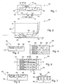
- a sensor device 100 for detecting biological particles will be explained.
- the sensor device 100 comprises a silicon substrate 102.
- a p + -doped region 104 is formed in a surface portion of the substrate 102 by a p-dopant implantation.
- a second doped region 106 namely an n + -doped region, is formed in another surface portion of the substrate 102 by implanting an n-dopant of an n-type of conductivity which differs from the p-type of conductivity of the p + -doped region 104.
- an optional lowly doped region 150 is formed in a surface portion of the substrate 102, which has an n - -dopant concentration that is significantly smaller than the dopant concentrations in the first and second doped regions 104, 106.
- a depletion region 108 is formed at a junction between the two oppositely doped regions 104, 150.
- a sensor active region 110 is configured to influence a property of the depletion region 108 (or more precisely of the diode structure 104, 106, 108, 150), particularly a size of the depletion region 108 which may have an impact on a current-voltage correlation of the diode-like configuration, in the presence of electrically charged particles to be detected.
- the sensing region 110 can be exactly on top of the depletion region 108.
- a detection unit 112 is provided which may be a CPU (Central Processing Unit) or microprocessor which may be adapted to detect the particles based on an electric measurement performed upon application of a predetermined reference voltage between the first doped region 104 and the second doped region 106, the electric measurement being indicative of the presence of the particles in the sensor active region 110.
- the measurement may be performed at a predetermined reference voltage, particularly at a breakdown voltage estimated in the sample free state of the sensor device 100. It is possible to evaluate the breakdown voltage and the I(V) curves, which change when the size of the depletion region 108 changes.
- the detection unit 112 is adapted to apply a predetermined reference voltage between the first doped region 104 and the second doped region 106 and to perform an electric measurement to detect the particles based on an evaluation of the electric measurement being sensitive to the property of the depletion region 108.
- the sensor active region 110 is provided on or over the depletion region 108.
- the sensor active region 110 comprises capture particles 114 adapted for attachment with the particles to be detected.
- a dielectric layer 116 is provided between the capture particles 114 and the depletion region 108.
- the detection unit 112 controls the voltage V of a voltage source 120. Further, the detection unit 112 is in bidirectional communication with a current detector 122 or Amperemeter.
- the detection unit 112 is further coupled to an input/output unit 124. Via the input/output unit 124, a user may enter control commands or may receive detection results from the detection unit 112.
- the detection unit 112 may be adapted for detecting the particles by first determining the predetermined voltage as a breakdown voltage of the diode formed by the first doped region 104 and the second doped region 106 in the absence of the particles. Then, the Amperemeter 122 at the breakdown voltage of the arrangement may measure an electric current in the absence of the particles. Subsequently, the Amperemeter 122 in the presence of the particles may measure the electric current. This measurement may be performed at the breakdown voltage of the arrangement determined beforehand in the absence of the particles. Subsequently, the detection unit 112 may compare the electric current values measured in the presence of the particles and in the absence of the particles, and may derive a sensor result therefrom.
- a sensing device 100 is provided using a shift in the breakdown voltage of a reverse biased diode 104, 106, 108, 150.
- the breakdown voltage of the pn diode 104, 106, 108, 150 in reverse bias is closely related to the size of the diode depletion region 108.
- the depletion region 108 size, and thus the breakdown voltage can be increased by adding an optional lowly doped region 150 between the p + region 104 and the n + region 106.
- the breakdown voltage can be tuned by applying an external potential to this lowly doped region. Therefore, a change in the external potential on top of the lowly doped region 108 induced by the attachment of charged particles to the capture particles 114 will modify the breakdown voltage of the diode 104, 106, 108, 150.
- the above-described effect may be used to detect the presence of charged particles. This will be described referring to Fig. 2 .
- Fig. 2 is a diagram 200 having an abscissa 202 along which the voltage is plotted in Volt. Along an ordinate 204, the current is plotted in Ampere.
- the voltage V BDO is shown as well in Fig. 2 for the diode 104, 106, 108, 150 of Fig. 1 .
- a characteristic curve 206 is measured.
- a second curve 208 is measured.
- the current value at the voltage V BDO significantly differs (compare I after , I before ).
- a first measurement 206 determines a voltage V BD0 , close the breakdown voltage of the diode 104, 106, 108, 150 and where the current increases a lot as a function of the potential, and measures the current at V BD0 .
- a second measurement 208 determines the current also at V BD0 . Because the measurements occur in the range of the breakdown voltage, the simulations show that the difference in the current between both measurements can be of several orders of magnitude.
- the high-voltage devices are a background because described herein makes use of the techniques (lowly-doped region, modification of the size of the depletion region by an external potential) that are used in their field.
- a main challenge in high voltage devices is to make diodes that can withstand a high voltage difference without breakdown. This increase in the breakdown voltage is often achieved by integrating a large lowly doped drift region between the p-type and n-type regions, see Fig. 3, Fig. 4 .
- the dimensions and doping of the region 308 are adequately tuned, this increase in the breakdown voltage can be enhanced by the RESURF effect. Furthermore, applying a potential to the n-region may further modify the breakdown voltage of the diode.
- DIELER diodes are disclosed as such in WO 2006/136979 . Trenches filled with an isolator and located as shown in Fig. 5 to Fig. 7 will increase further the breakdown voltage of the diode.
- An alternative to the DIELER is to only partially fill the trenches with oxide and thus create conducting field plates in the trenches.
- Fig. 5 shows a top view 500 of a DIELER diode 500. As compared to Fig. 4 , a plurality of trenches 502 is provided.
- Fig. 6 shows a cross-sectional view 600 along a line B-B' of Fig. 5
- Fig. 7 shows a cross-sectional view 700 along a line C-C' of Fig. 5 .
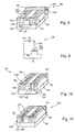
- Fig. 8 shows a three-dimensional view 800 of a conventional DIELER diode 800.
- a buried oxide layer 802 is shown.
- An n - -external drain region 804 is provided thereon.
- a first n + source/drain region 806 and a second n + source/drain region 808 are shown.
- a gate 810 is shown.
- Trenches 812 are formed having a dielectric layer 814 and an electrically conductive field plate 816.
- a p-well 818 is shown.
- Fig. 9 shows a conventional FET sensor 900.
- a counter electrode 902 is coupled to a voltage source V CE 904, which voltage source is further coupled to a transistor 906 having a gate being coupled to a detection electrode 908.
- a further voltage source 910 V ds is shown as well.
- the liquid containing the species to detect is in contact with the counter electrode 902 (sometimes called reference electrode) and a detection electrode 908.
- the detection electrode 908 is connected to the gate of the transistor 906.
- the detection of an event resulting in a change in the gate potential is made by a measurement in a change of the source/drain current.
- Fig. 10 shows a sensor device 1100 according to an embodiment of the invention.
- the sensor device 1100 comprises a plurality of trenches 1102 filled partially with dielectric material 1104 and extending from the first doped region 104 via the lowly-doped region 108 to the second doped region 106.
- the sensor device 1100 comprises an electrically conductive inlay 1106 in the dielectric material 1104 of the plurality of trenches 1102.
- the trenches 1102 are part of the sensor active region 110.
- Fig. 10 shows a scenario in which particles to be detected 1120 are provided functionally coupled to the field plates 1106.
- the particles 1120 are provided within the trenches 1102.
- the charged particles 1120 to detect can either be on top of fields plates 1106 ( Fig. 10 ) or the STI 1104 can be empty and the charged particles 1120 come in the place of the field plates 1106 (see Fig. 11 ). There, the area coverage by the external potential induced by the charge attached will even be larger than with the "basic" diode. Thus a higher difference in the breakdown voltage may be possible.
- the sensor of Fig. 1 (simple diode) is very easy to build with doping a piece of monocrystalline silicon or by using the technology of high-voltage CMOS. Taking into account the fact that the liquid should not be in contact with the electrical connections, several solutions for this problem are possible. It is possible to give to the liquid a direct access to the detection electrode or to build the interconnect structure of the circuit and to have the electrode included in this interconnect structure.
- Fig. 12 shows a cross-sectional view 1400 of a layer sequence .
- the layer sequence 1400 includes a further p-conductive layer 1402 below an interconnect structure 1404 which includes contacts 1406, 1408 to the first and second doped regions 104, 106, respectively.
- Fig. 12 shows a wafer with an interconnect structure.
- Fig. 13 shows a layer sequence 1500, in which the wafer 102 is grinded to provide liquid access.
- Fig. 14 shows a layer sequence 1600, in which an oxide layer 1602 is created, and charged particles 1604 are deposited thereon.
- silicon on nothing vias may be implemented. This may use a silicon-on-nothing method, like the one shown in Fig. 15 to Fig. 17 .
- Fig. 15 shows an image 1700 regarding spherical ESS.
- An image 1800 shown in Fig. 16 relates to pipe shaped ESS.
- An image 1900 shown in Fig. 17 relates to plate shaped ESS.
- Fig. 18 to Fig. 21 illustrate the use of a silicon-on-nothing system to bring the liquid close to the detection electrode.
- Fig. 18 to Fig. 21 show the fabrication of a silicon-on-nothing device 2300.
- a hole 2000 is formed in the substrate 102.
- An interconnect structure 1404 is then formed, as can be taken from Fig. 19 .
- vias 2200 are etched, and a silicon oxide layer 1602 is created in the hole 2000.
- Fig. 21 then shows a liquid motion direction 2302.
- a sensor according to the invention is capable to measure the difference between two situations: a reference situation and detection itself.
- the measurement protocol may be the following:
- Fig. 22 to Fig. 25 illustrate particles sensing, these particles being DNA.
- a solution with highly concentrated DNA 2500 is measured.
- a measurement with known strand of DNA 2600 is performed.
- Fig. 25 attachment between the strands 2600 and test DNA 2700 occurs.
- a sensor device 2800 for detecting biological particles will be explained.
- Fig. 26, Fig. 27, Fig. 29 and Fig. 30 illustrate layer sequences used for explaining a working principle of the sensor device 2800, which is shown in Fig. 28 .
- the sensor of Fig. 28 omits the central lowly-doped region n - 150 of Fig.1 .
- a diode is formed of a p-doped region 104 and an n-doped region 106.
- the fact that these regions 104, 106 are in contact with each other creates at their junction a depletion region 108.
- the breakdown voltage of the diode depends on the size of this depletion region 108.
- Fig. 28 shows that the central lowly-doped region 150 is not needed.
- the breakdown voltage depends on the size of the depletion region 108 which in turn depends on the doping concentration. Therefore, a way to increase the breakdown voltage of a diode is to add a lowly doped region 150 (n - for example but it can be p - ) between the p and n regions 104, 106, see Fig. 1 , Fig. 29, Fig. 30 . In that case, the depletion region 108 will be localized at the junction between the p and n - regions 104, 150 and it may extend more in the n - region 150 than in the p region 104 (see Fig. 30 ). It may sometimes be so large that it extends to the n region 106.
Landscapes
- Health & Medical Sciences (AREA)
- Life Sciences & Earth Sciences (AREA)
- Chemical & Material Sciences (AREA)
- Molecular Biology (AREA)
- Physics & Mathematics (AREA)
- Chemical Kinetics & Catalysis (AREA)
- Microelectronics & Electronic Packaging (AREA)
- Engineering & Computer Science (AREA)
- Spectroscopy & Molecular Physics (AREA)
- Electrochemistry (AREA)
- Analytical Chemistry (AREA)
- Biochemistry (AREA)
- General Health & Medical Sciences (AREA)
- General Physics & Mathematics (AREA)
- Immunology (AREA)
- Pathology (AREA)
- Investigating Or Analyzing Materials By The Use Of Electric Means (AREA)
Claims (15)
- Eine Sensorvorrichtung (100, 2800) zum Detektieren von Partikeln, die Sensorvorrichtung (100, 2800) aufweisend:ein Substrat (102);einen ersten dotierten Bereich (104), welcher in dem Substrat (102) mittels eines ersten Dotierstoffs von einer ersten Art von Konduktivität gebildet ist;einen zweiten dotierten Bereich (106, 150), welcher in dem Substrat (102) mittels eines zweiten Dotierstoffs von einer zweiten Art von Konduktivität gebildet wird, welcher sich von der ersten Art von Konduktivität unterscheidet;einen Verarmungsbereich (108) an einer Grenzzone zwischen dem ersten dotieren Bereich (104) und dem zweiten dotiertem Bereich (106, 150);einen sensoraktiven Bereich (110), welcher adaptiert ist, um eine Eigenschaft von dem Verarmungsbereich (108) in Anwesenheit der Partikel zu beeinflussen;eine Detektierungseinheit (112), welche adaptiert ist die Partikel, basierend auf einer elektrischen Messung zu detektieren, welche bei Beaufschlagung von einer vorbestimmten Referenzspannung zwischen dem ersten dotieren Bereich (104) und dem zweiten dotieren Bereich (106, 150) ausgeführt wird, wobei die elektrische Messung für die Anwesenheit der Partikel in dem sensoraktiven Bereich (104) indikativ ist;dadurch gekennzeichnet, dass das Substrat (102) eine Mehrzahl von Gräben (1102) aufweist, welche zumindest teilweise mit dielektrischem Material (1104) gefüllt sind und welche sich von dem ersten dotierten Bereich (104) zu dem zweiten dotierten Bereich (106, 150) erstrecken; unddass die Detektierungseinheit (112) zum Detektieren der Partikel adaptiert ist mittels Bestimmen der vorbestimmten Referenzspannung als eine Durchschlagsspannung einer Andordnung, welche mittels des ersten dotierten Bereichs (104), des zweiten dotieren Bereichs (106, 150) und des Verarmungsbereichs (108) in Abwesenheit der Partikel gebildet wird;Messen eines elektrischen Stroms bei der Durchschlagsspannung der Anordnung in Abwesenheit der Partikel;Messen, in Anwesenheit der Partikel einen elektrischen Strom bei der Durchschlagsspannung der Anordnung, welche in Abwesenheit der Partikel ermittelt wurde;Vergleichen des elektrischen Stroms, welcher in Anwesenheit der Partikel und in Abwesenheit der Partikel gemessen wurde.
- Die Sensorvorrichtung (1100) gemäß Anspruch 1, welche ein elektrisch konduktives Inlay (1106) in dem dielektrischen Material (1104) von zumindest einem Teil der Mehrzahl der Gräben (1102) aufweist.
- Die Sensorvorrichtung (1100) gemäß Anspruch 1 oder 2,
wobei die Mehrzahl der Gräben (1102) ein Teil des sensoraktiven Bereichs (110) ist. - Die Sensorvorrichtung (100, 2800) gemäß Anspruch 1,
wobei der erste dotierte Bereich (104) ein p-dotierter Bereich und der zweite dotierte Bereich (106,150) ein n-dotierter Bereich ist. - Die Sensorvorrichtung (100, 2800) gemäß Anspruch 1,
wobei der sensoraktive Bereich (100) adaptiert ist, um einen Wert der Durchschlagsspannung der Anordnung zu beeinflussen, welche mittels des ersten dotierten Bereichs (104), des zweiten dotierten Bereichs (106, 150) und des Verarmungsbereichs (108) in Anwesenheit der Partikel gebildet wird. - Die Sensorvorrichtung (100, 2800) gemäß Anspruch 1,
wobei sich der sensoraktive Bereich (110) unmittelbar ab dem Verarmungsbereich befindet. - Die Sensorvorrichtung (100, 2800) gemäß Anspruch 1,
wobei der sensoraktive Bereich (110) Einfang-Partikel (114) aufweist, welche zum Anlagern an die Partikel adaptiert sind. - Die Sensorvorrichtung (100, 2800) gemäß Anspruch 7,
wobei der sensoraktive Bereich (110) eine dielektrische Schicht (116) zwischen den Einfang-Partikel (114) und dem Verarmungsbereich (108) aufweist. - Die Sensorvorrichtung (100, 2800) gemäß Anspruch 1,
wobei die Detektierungseinheit (112) adaptiert ist, um die Partikel zu detektieren mittels Durchführens der elektrischen Messung bei genau oder ungefähr einer Durchschlagsspannung, wie die vorbestimmte Referenzspannung von einer Anordnung, welche mittels dem ersten dotieren Bereich (104), dem zweiten dotierten Bereich (106, 150) und dem Verarmungsbereich (108) gebildet ist. - Die Sensorvorrichtung (100, 2800) gemäß Anspruch 1, welche zum Detektieren von elektrisch aufgeladenen Partikeln adaptiert ist.
- Die Sensorvorrichtung (100, 2800) gemäß Anspruch 1, welche derart adaptiert ist, dass eine flüssige Probe, welche Partikel beinhaltet, frei ist von einem Kotakt mit den elektrischen Verbindungen der Sensorvorrichtung (100, 2800).
- Die Sensorvorrichtung (100, 2800) gemäß Anspruch 1,
wobei der Eigenschaft eine Größe des Verarmungsbereichs (108) ist. - Die Sensorvorrichtung (100, 2800) gemäß Anspruch 1,
wobei der Verarmungsbereich (108) eine Konzentration von Ladungsträgern hat, welche zumindest 102 fach, insbesondere zumindest 103 fach, weiter insbesondere zumindest 104 fach kleiner ist als eine Konzentration von Ladungsträgern in dem ersten dotierten Bereich (104) und/oder in dem zweiten dotierten Bereich (106, 150). - Die Sensorvorrichtung (100) gemäß Anspruch 1,
wobei der zweite dotierte Bereich (106,150) einen hoch dotierten Bereich (106) und einen niedrig dotierten Bereich (150) aufweist, wobei der niedrig dotierte Bereich (150) an den ersten dotieren Bereich angrenzend angeordnet ist, um die Verarmungszone (108) an einer Grenzzone mit dem ersten dotierten Bereich (104) zu bilden. - Die Sensorvorrichtung (100) gemäß Anspruch 1,
welche adaptiert ist als eine von einer Gruppe bestehend aus einer Biosensorvorrichtung, einer chemischen Sensorvorrichtung, einer pH Sensorvorrichtung, einer enzymatischen Sensorvorrichtung, einer DNA Sensorvorrichtung, und einer Protein Sensorvorrichtung.
Priority Applications (1)
| Application Number | Priority Date | Filing Date | Title |
|---|---|---|---|
| EP09721177A EP2255177B1 (de) | 2008-03-14 | 2009-03-09 | Sensorvorrichtung zur erkennung von partikeln |
Applications Claiming Priority (3)
| Application Number | Priority Date | Filing Date | Title |
|---|---|---|---|
| EP08102607 | 2008-03-14 | ||
| PCT/IB2009/050976 WO2009113013A2 (en) | 2008-03-14 | 2009-03-09 | A sensor device and a method of detecting particles |
| EP09721177A EP2255177B1 (de) | 2008-03-14 | 2009-03-09 | Sensorvorrichtung zur erkennung von partikeln |
Publications (2)
| Publication Number | Publication Date |
|---|---|
| EP2255177A2 EP2255177A2 (de) | 2010-12-01 |
| EP2255177B1 true EP2255177B1 (de) | 2012-06-20 |
Family
ID=40943838
Family Applications (1)
| Application Number | Title | Priority Date | Filing Date |
|---|---|---|---|
| EP09721177A Not-in-force EP2255177B1 (de) | 2008-03-14 | 2009-03-09 | Sensorvorrichtung zur erkennung von partikeln |
Country Status (3)
| Country | Link |
|---|---|
| US (1) | US9799757B2 (de) |
| EP (1) | EP2255177B1 (de) |
| WO (1) | WO2009113013A2 (de) |
Cited By (1)
| Publication number | Priority date | Publication date | Assignee | Title |
|---|---|---|---|---|
| US10168477B2 (en) | 2014-04-02 | 2019-01-01 | International Business Machines Corporation | Integration of photonic, electronic, and sensor devices with SOI VLSI microprocessor technology |
Families Citing this family (6)
| Publication number | Priority date | Publication date | Assignee | Title |
|---|---|---|---|---|
| US20150268184A1 (en) * | 2014-03-18 | 2015-09-24 | Georgia Tech Research Corporation | Gas sensors using magnetic fields and methods of use thereof |
| US10030265B2 (en) | 2015-01-14 | 2018-07-24 | International Business Machines Corporation | DNA sequencing using MOSFET transistors |
| US10656088B2 (en) | 2016-08-12 | 2020-05-19 | Silanna UV Technologies Pte Ltd | Ultraviolet biosensor |
| IT201800004621A1 (it) | 2018-04-17 | 2019-10-17 | Dispositivo optoelettronico ad elevata sensibilita' per la rilevazione di specie chimiche e relativo metodo di fabbricazione | |
| IT201800004620A1 (it) | 2018-04-17 | 2019-10-17 | Dispositivo a semiconduttore ad elevata sensibilita' per la rilevazione di specie chimiche fluide e relativo metodo di fabbricazione | |
| IT201800004622A1 (it) | 2018-04-17 | 2019-10-17 | Fotorilevatore includente un fotodiodo a valanga operante in modalita' geiger e un resistore integrato e relativo metodo di fabbricazione |
Family Cites Families (17)
| Publication number | Priority date | Publication date | Assignee | Title |
|---|---|---|---|---|
| US4103227A (en) * | 1977-03-25 | 1978-07-25 | University Of Pennsylvania | Ion-controlled diode |
| US5434442A (en) * | 1990-07-02 | 1995-07-18 | Motorola, Inc. | Field plate avalanche diode |
| JPH053337A (ja) * | 1990-11-28 | 1993-01-08 | Hitachi Ltd | 半導体放射線検出装置及び半導体放射線検出器並びにその製造方法 |
| GB2278235B (en) * | 1991-10-21 | 1996-05-08 | Holm Kennedy James W | Method and device for biochemical sensing |
| DE4343365A1 (de) * | 1993-12-18 | 1995-07-13 | Bosch Gmbh Robert | Driftfreie Lawinendurchbruchdiode |
| US5394735A (en) * | 1993-12-20 | 1995-03-07 | National Science Council | Gas sensor |
| US6627959B1 (en) * | 2002-04-16 | 2003-09-30 | Boston Microsystems, Inc. | P-n junction sensor |
| US7498657B2 (en) * | 2002-10-10 | 2009-03-03 | Taiwan Semiconductor Manufacturing Co., Ltd. | Vertical resistors and band-gap voltage reference circuits |
| FR2857952B1 (fr) * | 2003-07-25 | 2005-12-16 | St Microelectronics Sa | Resonateur electromecanique et procede de fabrication d'un tel resonateur |
| US7692219B1 (en) * | 2004-06-25 | 2010-04-06 | University Of Hawaii | Ultrasensitive biosensors |
| US7488991B2 (en) * | 2004-12-03 | 2009-02-10 | Yeda Research And Development Co. Ltd. | Molecular controlled semiconductor device |
| US7808050B2 (en) * | 2005-06-22 | 2010-10-05 | Nxp B.V. | Semiconductor device with relatively high breakdown voltage and manufacturing method |
| JP2009521126A (ja) * | 2005-12-22 | 2009-05-28 | エヌエックスピー ビー ヴィ | フィールドプレートを具える半導体デバイス及びその製造方法 |
| US20090250696A1 (en) * | 2006-06-04 | 2009-10-08 | Guy Silver | Near natural breakdown device |
| US8188548B2 (en) * | 2007-02-15 | 2012-05-29 | Infineon Technologies Ag | Device and method for reducing a voltage dependent capacitive coupling |
| US9034637B2 (en) * | 2007-04-25 | 2015-05-19 | Nxp, B.V. | Apparatus and method for molecule detection using nanopores |
| US20100052080A1 (en) | 2007-04-27 | 2010-03-04 | Nxp B.V. | Biosensor chip and a method of manufacturing the same |
-
2009
- 2009-03-09 WO PCT/IB2009/050976 patent/WO2009113013A2/en not_active Ceased
- 2009-03-09 EP EP09721177A patent/EP2255177B1/de not_active Not-in-force
- 2009-03-09 US US12/922,665 patent/US9799757B2/en not_active Expired - Fee Related
Cited By (2)
| Publication number | Priority date | Publication date | Assignee | Title |
|---|---|---|---|---|
| US10168477B2 (en) | 2014-04-02 | 2019-01-01 | International Business Machines Corporation | Integration of photonic, electronic, and sensor devices with SOI VLSI microprocessor technology |
| US10168478B2 (en) | 2014-04-02 | 2019-01-01 | International Business Machines Corporation | Integration of photonic, electronic, and sensor devices with SOI VLSI microprocessor technology |
Also Published As
| Publication number | Publication date |
|---|---|
| US20110204872A1 (en) | 2011-08-25 |
| EP2255177A2 (de) | 2010-12-01 |
| WO2009113013A3 (en) | 2009-11-05 |
| US9799757B2 (en) | 2017-10-24 |
| WO2009113013A2 (en) | 2009-09-17 |
Similar Documents
| Publication | Publication Date | Title |
|---|---|---|
| US20240377352A1 (en) | High sensitivity isfet sensor | |
| EP2142666B1 (de) | Vorrichtung zur molekülerkennung mithilfe von nanoporen | |
| US9799757B2 (en) | PN junction chemical sensor | |
| US10184912B2 (en) | Backside sensing BioFET with enhanced performance | |
| US11008611B2 (en) | Double gate ion sensitive field effect transistor | |
| US7893466B2 (en) | Semiconductor FET sensor and method of fabricating the same | |
| EP2293053A1 (de) | Sensor und verfahren zu seiner herstellung | |
| KR100906154B1 (ko) | 반도체 나노선 센서 소자 및 이의 제조 방법 | |
| EP2140256A2 (de) | Biosensorchip und herstellungsverfahren dafür | |
| WO2012125727A1 (en) | Calibration of nanostructure sensors | |
| US11320394B2 (en) | Biosensor electrode having three-dimensional structured sensing surfaces | |
| US20210325339A1 (en) | Biosensor Devices and Methods of Forming the Same | |
| Knopfmacher et al. | Dual gated silicon nanowire field effect transistors | |
| US20250116629A1 (en) | Semiconductor biosensor | |
| US9746442B2 (en) | Switched-capacitor biosensor device | |
| US20260118312A1 (en) | Microwell sensor and reference electrode semiconductor structures and methods of forming same | |
| WO2008068692A1 (en) | Method of manufacturing a semiconductor sensor device and semiconductor sensor device obtained with such method | |
| Ha et al. | Process Integration of Ion Sensitive Field Effect Transistor Bio-Sensor Array Platform |
Legal Events
| Date | Code | Title | Description |
|---|---|---|---|
| PUAI | Public reference made under article 153(3) epc to a published international application that has entered the european phase |
Free format text: ORIGINAL CODE: 0009012 |
|
| 17P | Request for examination filed |
Effective date: 20101014 |
|
| AK | Designated contracting states |
Kind code of ref document: A2 Designated state(s): AT BE BG CH CY CZ DE DK EE ES FI FR GB GR HR HU IE IS IT LI LT LU LV MC MK MT NL NO PL PT RO SE SI SK TR |
|
| AX | Request for extension of the european patent |
Extension state: AL BA RS |
|
| DAX | Request for extension of the european patent (deleted) | ||
| REG | Reference to a national code |
Ref country code: DE Ref legal event code: R079 Ref document number: 602009007731 Country of ref document: DE Free format text: PREVIOUS MAIN CLASS: G01N0027000000 Ipc: G01N0027414000 |
|
| GRAP | Despatch of communication of intention to grant a patent |
Free format text: ORIGINAL CODE: EPIDOSNIGR1 |
|
| RIC1 | Information provided on ipc code assigned before grant |
Ipc: H01L 29/739 20060101ALI20120112BHEP Ipc: G01N 27/414 20060101AFI20120112BHEP |
|
| RTI1 | Title (correction) |
Free format text: SENSOR DEVICE FOR DETECTING PARTICLES |
|
| GRAS | Grant fee paid |
Free format text: ORIGINAL CODE: EPIDOSNIGR3 |
|
| GRAA | (expected) grant |
Free format text: ORIGINAL CODE: 0009210 |
|
| AK | Designated contracting states |
Kind code of ref document: B1 Designated state(s): AT BE BG CH CY CZ DE DK EE ES FI FR GB GR HR HU IE IS IT LI LT LU LV MC MK MT NL NO PL PT RO SE SI SK TR |
|
| REG | Reference to a national code |
Ref country code: GB Ref legal event code: FG4D |
|
| REG | Reference to a national code |
Ref country code: CH Ref legal event code: EP |
|
| REG | Reference to a national code |
Ref country code: AT Ref legal event code: REF Ref document number: 563326 Country of ref document: AT Kind code of ref document: T Effective date: 20120715 |
|
| REG | Reference to a national code |
Ref country code: IE Ref legal event code: FG4D |
|
| REG | Reference to a national code |
Ref country code: DE Ref legal event code: R096 Ref document number: 602009007731 Country of ref document: DE Effective date: 20120816 |
|
| PG25 | Lapsed in a contracting state [announced via postgrant information from national office to epo] |
Ref country code: SE Free format text: LAPSE BECAUSE OF FAILURE TO SUBMIT A TRANSLATION OF THE DESCRIPTION OR TO PAY THE FEE WITHIN THE PRESCRIBED TIME-LIMIT Effective date: 20120620 Ref country code: NO Free format text: LAPSE BECAUSE OF FAILURE TO SUBMIT A TRANSLATION OF THE DESCRIPTION OR TO PAY THE FEE WITHIN THE PRESCRIBED TIME-LIMIT Effective date: 20120920 Ref country code: LT Free format text: LAPSE BECAUSE OF FAILURE TO SUBMIT A TRANSLATION OF THE DESCRIPTION OR TO PAY THE FEE WITHIN THE PRESCRIBED TIME-LIMIT Effective date: 20120620 Ref country code: FI Free format text: LAPSE BECAUSE OF FAILURE TO SUBMIT A TRANSLATION OF THE DESCRIPTION OR TO PAY THE FEE WITHIN THE PRESCRIBED TIME-LIMIT Effective date: 20120620 |
|
| REG | Reference to a national code |
Ref country code: NL Ref legal event code: VDEP Effective date: 20120620 |
|
| REG | Reference to a national code |
Ref country code: AT Ref legal event code: MK05 Ref document number: 563326 Country of ref document: AT Kind code of ref document: T Effective date: 20120620 |
|
| REG | Reference to a national code |
Ref country code: LT Ref legal event code: MG4D Effective date: 20120620 |
|
| PG25 | Lapsed in a contracting state [announced via postgrant information from national office to epo] |
Ref country code: HR Free format text: LAPSE BECAUSE OF FAILURE TO SUBMIT A TRANSLATION OF THE DESCRIPTION OR TO PAY THE FEE WITHIN THE PRESCRIBED TIME-LIMIT Effective date: 20120620 Ref country code: SI Free format text: LAPSE BECAUSE OF FAILURE TO SUBMIT A TRANSLATION OF THE DESCRIPTION OR TO PAY THE FEE WITHIN THE PRESCRIBED TIME-LIMIT Effective date: 20120620 Ref country code: LV Free format text: LAPSE BECAUSE OF FAILURE TO SUBMIT A TRANSLATION OF THE DESCRIPTION OR TO PAY THE FEE WITHIN THE PRESCRIBED TIME-LIMIT Effective date: 20120620 Ref country code: GR Free format text: LAPSE BECAUSE OF FAILURE TO SUBMIT A TRANSLATION OF THE DESCRIPTION OR TO PAY THE FEE WITHIN THE PRESCRIBED TIME-LIMIT Effective date: 20120921 |
|
| PG25 | Lapsed in a contracting state [announced via postgrant information from national office to epo] |
Ref country code: AT Free format text: LAPSE BECAUSE OF FAILURE TO SUBMIT A TRANSLATION OF THE DESCRIPTION OR TO PAY THE FEE WITHIN THE PRESCRIBED TIME-LIMIT Effective date: 20120620 Ref country code: RO Free format text: LAPSE BECAUSE OF FAILURE TO SUBMIT A TRANSLATION OF THE DESCRIPTION OR TO PAY THE FEE WITHIN THE PRESCRIBED TIME-LIMIT Effective date: 20120620 Ref country code: EE Free format text: LAPSE BECAUSE OF FAILURE TO SUBMIT A TRANSLATION OF THE DESCRIPTION OR TO PAY THE FEE WITHIN THE PRESCRIBED TIME-LIMIT Effective date: 20120620 Ref country code: CY Free format text: LAPSE BECAUSE OF FAILURE TO SUBMIT A TRANSLATION OF THE DESCRIPTION OR TO PAY THE FEE WITHIN THE PRESCRIBED TIME-LIMIT Effective date: 20120620 Ref country code: BE Free format text: LAPSE BECAUSE OF FAILURE TO SUBMIT A TRANSLATION OF THE DESCRIPTION OR TO PAY THE FEE WITHIN THE PRESCRIBED TIME-LIMIT Effective date: 20120620 Ref country code: SK Free format text: LAPSE BECAUSE OF FAILURE TO SUBMIT A TRANSLATION OF THE DESCRIPTION OR TO PAY THE FEE WITHIN THE PRESCRIBED TIME-LIMIT Effective date: 20120620 Ref country code: IS Free format text: LAPSE BECAUSE OF FAILURE TO SUBMIT A TRANSLATION OF THE DESCRIPTION OR TO PAY THE FEE WITHIN THE PRESCRIBED TIME-LIMIT Effective date: 20121020 Ref country code: CZ Free format text: LAPSE BECAUSE OF FAILURE TO SUBMIT A TRANSLATION OF THE DESCRIPTION OR TO PAY THE FEE WITHIN THE PRESCRIBED TIME-LIMIT Effective date: 20120620 |
|
| PG25 | Lapsed in a contracting state [announced via postgrant information from national office to epo] |
Ref country code: PL Free format text: LAPSE BECAUSE OF FAILURE TO SUBMIT A TRANSLATION OF THE DESCRIPTION OR TO PAY THE FEE WITHIN THE PRESCRIBED TIME-LIMIT Effective date: 20120620 Ref country code: IT Free format text: LAPSE BECAUSE OF FAILURE TO SUBMIT A TRANSLATION OF THE DESCRIPTION OR TO PAY THE FEE WITHIN THE PRESCRIBED TIME-LIMIT Effective date: 20120620 Ref country code: PT Free format text: LAPSE BECAUSE OF FAILURE TO SUBMIT A TRANSLATION OF THE DESCRIPTION OR TO PAY THE FEE WITHIN THE PRESCRIBED TIME-LIMIT Effective date: 20121022 |
|
| PG25 | Lapsed in a contracting state [announced via postgrant information from national office to epo] |
Ref country code: NL Free format text: LAPSE BECAUSE OF FAILURE TO SUBMIT A TRANSLATION OF THE DESCRIPTION OR TO PAY THE FEE WITHIN THE PRESCRIBED TIME-LIMIT Effective date: 20120620 |
|
| PLBE | No opposition filed within time limit |
Free format text: ORIGINAL CODE: 0009261 |
|
| STAA | Information on the status of an ep patent application or granted ep patent |
Free format text: STATUS: NO OPPOSITION FILED WITHIN TIME LIMIT |
|
| PG25 | Lapsed in a contracting state [announced via postgrant information from national office to epo] |
Ref country code: ES Free format text: LAPSE BECAUSE OF FAILURE TO SUBMIT A TRANSLATION OF THE DESCRIPTION OR TO PAY THE FEE WITHIN THE PRESCRIBED TIME-LIMIT Effective date: 20121001 Ref country code: DK Free format text: LAPSE BECAUSE OF FAILURE TO SUBMIT A TRANSLATION OF THE DESCRIPTION OR TO PAY THE FEE WITHIN THE PRESCRIBED TIME-LIMIT Effective date: 20120620 |
|
| 26N | No opposition filed |
Effective date: 20130321 |
|
| REG | Reference to a national code |
Ref country code: DE Ref legal event code: R097 Ref document number: 602009007731 Country of ref document: DE Effective date: 20130321 |
|
| PG25 | Lapsed in a contracting state [announced via postgrant information from national office to epo] |
Ref country code: BG Free format text: LAPSE BECAUSE OF FAILURE TO SUBMIT A TRANSLATION OF THE DESCRIPTION OR TO PAY THE FEE WITHIN THE PRESCRIBED TIME-LIMIT Effective date: 20120920 |
|
| PG25 | Lapsed in a contracting state [announced via postgrant information from national office to epo] |
Ref country code: MC Free format text: LAPSE BECAUSE OF NON-PAYMENT OF DUE FEES Effective date: 20130331 |
|
| REG | Reference to a national code |
Ref country code: CH Ref legal event code: PL |
|
| REG | Reference to a national code |
Ref country code: IE Ref legal event code: MM4A |
|
| PG25 | Lapsed in a contracting state [announced via postgrant information from national office to epo] |
Ref country code: IE Free format text: LAPSE BECAUSE OF NON-PAYMENT OF DUE FEES Effective date: 20130309 Ref country code: CH Free format text: LAPSE BECAUSE OF NON-PAYMENT OF DUE FEES Effective date: 20130331 Ref country code: LI Free format text: LAPSE BECAUSE OF NON-PAYMENT OF DUE FEES Effective date: 20130331 |
|
| PG25 | Lapsed in a contracting state [announced via postgrant information from national office to epo] |
Ref country code: MT Free format text: LAPSE BECAUSE OF FAILURE TO SUBMIT A TRANSLATION OF THE DESCRIPTION OR TO PAY THE FEE WITHIN THE PRESCRIBED TIME-LIMIT Effective date: 20120620 |
|
| PG25 | Lapsed in a contracting state [announced via postgrant information from national office to epo] |
Ref country code: TR Free format text: LAPSE BECAUSE OF FAILURE TO SUBMIT A TRANSLATION OF THE DESCRIPTION OR TO PAY THE FEE WITHIN THE PRESCRIBED TIME-LIMIT Effective date: 20120620 |
|
| PG25 | Lapsed in a contracting state [announced via postgrant information from national office to epo] |
Ref country code: MK Free format text: LAPSE BECAUSE OF FAILURE TO SUBMIT A TRANSLATION OF THE DESCRIPTION OR TO PAY THE FEE WITHIN THE PRESCRIBED TIME-LIMIT Effective date: 20120620 Ref country code: LU Free format text: LAPSE BECAUSE OF NON-PAYMENT OF DUE FEES Effective date: 20130309 Ref country code: HU Free format text: LAPSE BECAUSE OF FAILURE TO SUBMIT A TRANSLATION OF THE DESCRIPTION OR TO PAY THE FEE WITHIN THE PRESCRIBED TIME-LIMIT; INVALID AB INITIO Effective date: 20090309 |
|
| REG | Reference to a national code |
Ref country code: FR Ref legal event code: PLFP Year of fee payment: 8 |
|
| REG | Reference to a national code |
Ref country code: FR Ref legal event code: PLFP Year of fee payment: 9 |
|
| REG | Reference to a national code |
Ref country code: FR Ref legal event code: PLFP Year of fee payment: 10 |
|
| PGFP | Annual fee paid to national office [announced via postgrant information from national office to epo] |
Ref country code: GB Payment date: 20200221 Year of fee payment: 12 Ref country code: DE Payment date: 20200218 Year of fee payment: 12 |
|
| PGFP | Annual fee paid to national office [announced via postgrant information from national office to epo] |
Ref country code: FR Payment date: 20200220 Year of fee payment: 12 |
|
| REG | Reference to a national code |
Ref country code: DE Ref legal event code: R119 Ref document number: 602009007731 Country of ref document: DE |
|
| GBPC | Gb: european patent ceased through non-payment of renewal fee |
Effective date: 20210309 |
|
| PG25 | Lapsed in a contracting state [announced via postgrant information from national office to epo] |
Ref country code: GB Free format text: LAPSE BECAUSE OF NON-PAYMENT OF DUE FEES Effective date: 20210309 Ref country code: FR Free format text: LAPSE BECAUSE OF NON-PAYMENT OF DUE FEES Effective date: 20210331 Ref country code: DE Free format text: LAPSE BECAUSE OF NON-PAYMENT OF DUE FEES Effective date: 20211001 |