EP2251969A1 - Five-level inverter - Google Patents
Five-level inverter Download PDFInfo
- Publication number
- EP2251969A1 EP2251969A1 EP10002375A EP10002375A EP2251969A1 EP 2251969 A1 EP2251969 A1 EP 2251969A1 EP 10002375 A EP10002375 A EP 10002375A EP 10002375 A EP10002375 A EP 10002375A EP 2251969 A1 EP2251969 A1 EP 2251969A1
- Authority
- EP
- European Patent Office
- Prior art keywords
- terminal
- arm pair
- power source
- semiconductor devices
- midpoint
- Prior art date
- Legal status (The legal status is an assumption and is not a legal conclusion. Google has not performed a legal analysis and makes no representation as to the accuracy of the status listed.)
- Granted
Links
Images


Classifications
-
- H—ELECTRICITY
- H02—GENERATION; CONVERSION OR DISTRIBUTION OF ELECTRIC POWER
- H02M—APPARATUS FOR CONVERSION BETWEEN AC AND AC, BETWEEN AC AND DC, OR BETWEEN DC AND DC, AND FOR USE WITH MAINS OR SIMILAR POWER SUPPLY SYSTEMS; CONVERSION OF DC OR AC INPUT POWER INTO SURGE OUTPUT POWER; CONTROL OR REGULATION THEREOF
- H02M7/00—Conversion of ac power input into dc power output; Conversion of dc power input into ac power output
- H02M7/42—Conversion of dc power input into ac power output without possibility of reversal
- H02M7/44—Conversion of dc power input into ac power output without possibility of reversal by static converters
- H02M7/48—Conversion of dc power input into ac power output without possibility of reversal by static converters using discharge tubes with control electrode or semiconductor devices with control electrode
- H02M7/483—Converters with outputs that each can have more than two voltages levels
Definitions
- the invention relates to a power converter, in particular to a five-level inverter that can directly output five voltage levels.
- FIG. 5 shows one phase of a five-level inverter disclosed, for example, in Japanese Patent Application Laid-Open No. 2006-271042 .
- a serial circuit of semiconductor switches Q1 to Q8 is connected between a positive electrode and a negative electrode of a DC battery BA1 connected in series to DC unit power sources b1 to b4, and the connection point of the semiconductor switches Q4 and Q5 serves as an AC output point U.
- An external terminal of a diode arm pair DA1 formed by diodes D1 and D4 is connected between the connection point of the semiconductor switches Q1 and Q2 and between the connection point of Q5 and Q6, and the midpoint terminal of the diode arm pair is connected to the connection point of the DC unit power sources b1 and b2.
- the external terminal of the arm pair as referred to herein is a general name used to distinguish this terminal from the midpoint terminal, and in some cases the external terminal is omitted.
- an external terminal of a diode arm pair DA2 formed by diodes D2 and D5 is connected between the connection point of the semiconductor switches Q2 and Q3 and between the connection point of Q6 and Q7, and the midpoint terminal of the diode arm pair is connected to the connection point of the DC unit power sources b2 and b3.
- An external terminal of a diode arm pair DA3 formed by diodes D3 and D6 is connected between the connection point of the semiconductor switches Q3 and Q4 and between the connection point of Q7 and Q8, and the midpoint terminal of the diode arm pair is connected to the connection point of the DC unit power sources b3 and b4.
- the maximum number of semiconductor switches that pass an output current (also simply referred to as "current") between the DC battery BA1 and the AC output terminal U is four.
- the resultant problem is that the stationary ON loss in the semiconductor switch becomes large, the efficiency of the entire device decreases, and the device is difficult to reduce in size and cost. Accordingly, it is an object of the present invention to decrease the number of semiconductor switches that pass the electric current with respect to that in the conventional configuration, decrease the generated loss, and enable the reduction of the device is size and cost.
- the invention as set forth in claim 1 provides a five-level inverter that is provided with quartered five terminals and can select and output any voltage level from an input DC power source having five mutually different voltage levels including zero, the inverter comprising:
- the invention as set forth in claim 3 provides a five-level inverter that is provided with quartered five terminals and can select and output any voltage level from an input DC power source having five mutually different voltage levels including zero, the inverter comprising:
- each of the arms constituting the first to third arm pairs is selectively ON-OFF switched and driven so that only voltages of two or less fractions, from among the quartered DC power source voltages, are applied during the operation of the arms (claim 5).
- the maximum number of semiconductor switches through which a current passes between a DC power source serving as an input and an AC output is three. Therefore loss is reduced. As a result, the device is improved in efficiency and reduced in cost and size.
- FIG. 1 is a circuit diagram illustrating an embodiment of the invention.
- An external terminal of an arm pair QA1 composed of semiconductor switches Q1, Q2 is connected between a positive electrode and an intermediate (zero potential) terminal of a DC battery BA1 in which DC unit power sources b1 to b4, each having a 1E voltage, are connected in series, and an external terminal of an arm pair QA2 composed of Q3, Q4 is connected between the intermediate terminal and a negative electrode of the BA1.
- an external terminal of an arm pair QA3 composed of semiconductor switches Q5, Q6 is connected between the midpoint terminal of the arm pairs QA1 and QA2, and the midpoint terminal of the QA3 serves as an AC output terminal U.
- an AC switch SW1 composed of semiconductor switches Q11, Q12 is connected between the connection point of the DC unit power sources b1 and b2 and the midpoint terminal of QA1
- an AC switch SW2 composed of semiconductor switches Q13, Q14 is connected between the connection point of the DC unit power sources b3 and b4 and the midpoint terminal of QA2.
- FIG. 2 shows a modification example of the configuration shown in FIG. 1 .
- the difference between this configuration and that shown in FIG. 1 is that each inverse serial connection circuit of semiconductor switches Q11 and Q12, Q13 and Q14 constituting the AC switches SW1, SW2 is replaced with a corresponding inverse parallel circuit of respective reverse blocking IGBT Q21 and Q22, Q23 and Q24.
- the functions and action are not particularly different from those of the configuration with switches SW1, SW2 and the operation is identical to that of the configuration shown in FIG. 1 .
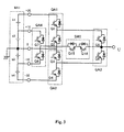
- FIG. 3 is a circuit diagram showing another embodiment of the invention.
- An external terminal of an arm pair QA1 composed of semiconductor switches Q1, Q2 is connected between a positive electrode and an intermediate terminal of a DC battery BA1 in which DC unit power sources b1 to b4, each having a 1E voltage, are connected in series, and an external terminal of an arm pair QA2 composed of Q3, Q4 is connected between the intermediate terminal and a negative electrode of the BA1.
- an external terminal of an arm pair QA3 composed of semiconductor switches Q5, Q6 is connected between the midpoint terminal of the arm pairs QA1 and QA2, and the midpoint terminal of the QA3 serves as an AC output terminal U.
- An external terminal of an arm pair QA4 composed of semiconductor switches Q7, Q8 is connected between the connection point of the DC unit power sources b1 and b2 and the connection point of b3 and b4, and an AC switch SW3 composed of semiconductor switches Q15, Q16 is connected between the midpoint points of the QA4 and QA3.
- a voltage applied to the semiconductor switches that have been switched OFF in QA1 to QA4 is clamped to a maximum 2E. Because of circuit symmetry, the operation of outputting -1E and -2E to the AC output point U is similar to that of outputting +1E, +2E, and the explanation thereof is omitted.
- FIG. 4 shows a modification example of the configuration shown in FIG. 3 .
- the difference between this configuration and that shown in FIG. 3 is that the inverted series connection circuit of semiconductor switches Q15 and Q16 constituting the AC switch SW3 is replaced with an inverted parallel circuit of Q25 and Q26 of reverse blocking IGBT.
- the functions and action are not particularly different from those of the configuration with the switch SW3 and the operation is identical to that of the configuration shown in FIG. 3 .
- each DC unit power source b1 to b4 is 400 V and a voltage of the DC battery is BA1 is 1600 V
- IGBT with a standard breakdown voltage of 1200 V can be applied to all the semiconductor switches Q1 to Q8, and IGBT or reverse blocking IGBT with a standard breakdown voltage of 600 V can be applied to the semiconductor switches Q11 to Q16 or reverse blocking IGBT Q21 to Q26.
- the output voltage of the AC output point U can be about AC 560 V as a phase voltage.
- the above-described five-level inverters can be combined for three phases, and a voltage output of equal to or higher than AC 1000 V can be obtained when a trapezoidal wave modulation system with a three harmonic superposition is used.
Abstract
Description
- The invention relates to a power converter, in particular to a five-level inverter that can directly output five voltage levels.
-
FIG. 5 shows one phase of a five-level inverter disclosed, for example, in Japanese Patent Application Laid-Open No.2006-271042
Referring toFIG. 5 , a serial circuit of semiconductor switches Q1 to Q8 is connected between a positive electrode and a negative electrode of a DC battery BA1 connected in series to DC unit power sources b1 to b4, and the connection point of the semiconductor switches Q4 and Q5 serves as an AC output point U. An external terminal of a diode arm pair DA1 formed by diodes D1 and D4 is connected between the connection point of the semiconductor switches Q1 and Q2 and between the connection point of Q5 and Q6, and the midpoint terminal of the diode arm pair is connected to the connection point of the DC unit power sources b1 and b2. The external terminal of the arm pair as referred to herein is a general name used to distinguish this terminal from the midpoint terminal, and in some cases the external terminal is omitted. - Likewise, an external terminal of a diode arm pair DA2 formed by diodes D2 and D5 is connected between the connection point of the semiconductor switches Q2 and Q3 and between the connection point of Q6 and Q7, and the midpoint terminal of the diode arm pair is connected to the connection point of the DC unit power sources b2 and b3. An external terminal of a diode arm pair DA3 formed by diodes D3 and D6 is connected between the connection point of the semiconductor switches Q3 and Q4 and between the connection point of Q7 and Q8, and the midpoint terminal of the diode arm pair is connected to the connection point of the DC unit power sources b3 and b4.
- In such a configuration, where the semiconductor switches Q1 to Q4 are ON and Q5 to Q8 are OFF, a voltage of a +2E level is outputted to the AC output terminal U, where the semiconductor switches Q2 to Q5 are ON and Q1, Q6 to Q8 are OFF, a voltage of a 1E level is outputted to the AC output terminal U, and where the semiconductor switches Q3 to Q6 are ON and Q1, Q2, Q7, and Q8 are OFF, a zero-level voltage is outputted to the AC output terminal U.
- Likewise, where the semiconductor switches Q4 to Q7 are ON and Q1 to Q3 and Q8 are OFF, a voltage of a -1E level is outputted to the AC output terminal U, and where the semiconductor switches Q5 to Q8 are ON and Q1 to Q4 are OFF, a voltage of a -2E level is outputted to the AC output terminal U.
As described hereinabove, by ON-OFF regulating the semiconductor switches Q1 to Q8, it is possible to output voltages of five different levels (2E, 1E, 0, -1E, -2E) to the AC output terminal U. - However, in the configuration shown in
FIG. 5 , the maximum number of semiconductor switches that pass an output current (also simply referred to as "current") between the DC battery BA1 and the AC output terminal U is four. The resultant problem is that the stationary ON loss in the semiconductor switch becomes large, the efficiency of the entire device decreases, and the device is difficult to reduce in size and cost.
Accordingly, it is an object of the present invention to decrease the number of semiconductor switches that pass the electric current with respect to that in the conventional configuration, decrease the generated loss, and enable the reduction of the device is size and cost. - In order to resolve the above-described problem, the invention as set forth in claim 1 provides a five-level inverter that is provided with quartered five terminals and can select and output any voltage level from an input DC power source having five mutually different voltage levels including zero, the inverter comprising:
- first, second, and third arm pairs each being configured by combining in series two arms formed of semiconductor devices, and first and second AC switches configured by inverse serially combining the arms formed of semiconductor devices, wherein
- the first arm pair is connected between a first DC terminal having the highest potential of the DC power source and a third DC terminal having an intermediate potential, the second arm pair is connected between the third DC terminal and a fifth DC terminal having the lowest potential, and the third arm pair is connected between the midpoint terminal of the first arm pair and the midpoint terminal of the second arm pair;
- the first AC switch is connected between a second DC terminal having the second highest potential of the DC power source and the midpoint terminal of the first arm pair, the second AC switch is connected between a fourth DC terminal having the fourth highest potential of the DC power source and the midpoint terminal of the second arm pair, and the midpoint terminal of the third arm pair serves as an output terminal.
- In the inverter according to the invention as set forth in claim 1, a configuration, in which arms formed of semiconductor devices are inverse serially combined, is replaced with a configuration, in which semiconductor devices with inverse withstand voltage are inverse parallel connected, as the first and second AC switches (invention as set forth in claim 2).
- The invention as set forth in claim 3 provides a five-level inverter that is provided with quartered five terminals and can select and output any voltage level from an input DC power source having five mutually different voltage levels including zero, the inverter comprising:
- first, second, third, and fourth arm pairs each being configured by combining in series two arms formed of semiconductor devices; and an AC switch configured by inverse serially combining the arms formed of semiconductor devices, wherein
- the first arm pair is connected between a first DC terminal having the highest potential of the DC power source and a third DC terminal having an intermediate potential, the second arm pair is connected between the third DC terminal and a fifth DC terminal having the lowest potential, the third arm pair is connected between the midpoint terminal of the first arm pair and the midpoint terminal of the second arm pair, and the fourth arm pair is connected between a second DC terminal having the second highest potential of the DC power source and a fourth DC terminal having the fourth highest potential of the DC power source;
- the AC switch is connected between a midpoint terminal of the fourth arm pair and a midpoint terminal of the third arm pair, and the midpoint terminal of the third arm pair serves as an output terminal.
- In the inverter according to the invention as set forth in claim 3, a configuration, in which arms formed of semiconductor devices are inverse serially combined, is replaced with a configuration, in which semiconductor devices with inverse withstand voltage are inverse parallel connected, as the AC switch (invention as set forth in claim 4). In the inverter according to the invention as set forth in any one of claims 1 to 4, each of the arms constituting the first to third arm pairs is selectively ON-OFF switched and driven so that only voltages of two or less fractions, from among the quartered DC power source voltages, are applied during the operation of the arms (claim 5).
- According to the invention, the maximum number of semiconductor switches through which a current passes between a DC power source serving as an input and an AC output is three. Therefore loss is reduced. As a result, the device is improved in efficiency and reduced in cost and size.
-
-
FIG. 1 is a circuit diagram illustrating an embodiment of the invention; -
FIG. 2 is a circuit diagram illustrating a modification example of the configuration shown inFIG. 1 ; -
FIG. 3 is a circuit diagram showing another embodiment of the invention; -
FIG. 4 is a circuit diagram illustrating a modification example of the configuration shown inFIG. 3 ; and -
FIG. 5 is a block diagram showing a conventional example of a five-level inverter. -
FIG. 1 is a circuit diagram illustrating an embodiment of the invention.
An external terminal of an arm pair QA1 composed of semiconductor switches Q1, Q2 is connected between a positive electrode and an intermediate (zero potential) terminal of a DC battery BA1 in which DC unit power sources b1 to b4, each having a 1E voltage, are connected in series, and an external terminal of an arm pair QA2 composed of Q3, Q4 is connected between the intermediate terminal and a negative electrode of the BA1. - Further, an external terminal of an arm pair QA3 composed of semiconductor switches Q5, Q6 is connected between the midpoint terminal of the arm pairs QA1 and QA2, and the midpoint terminal of the QA3 serves as an AC output terminal U. Further, an AC switch SW1 composed of semiconductor switches Q11, Q12 is connected between the connection point of the DC unit power sources b1 and b2 and the midpoint terminal of QA1, and an AC switch SW2 composed of semiconductor switches Q13, Q14 is connected between the connection point of the DC unit power sources b3 and b4 and the midpoint terminal of QA2.
- In the above-described configuration, when the semiconductor switches Q1, Q5 are switched ON and Q2, Q6, and AC switch SW1 are switched OFF, a +2E voltage is outputted to the AC output terminal U. In this case, a current passes through two semiconductor switches Q1, Q5. Where Q4 and SW2 are further switched OFF, a voltage applied to the semiconductor switches that have been switched OFF in QA1 to QA3 is clamped to a maximum of 2E. Likewise, a voltage applied to the semiconductor switches that have been switched OFF in the AC switches SW1 and SW2 is clamped to 1E.
- Where the AC switch SW1 and Q5 are switched ON and Q1, Q2, and Q6 are switched OFF, a +1E voltage is applied to the AC output terminal U. In this case a current passes through three semiconductor switches Q11, Q12, and Q5. Where Q4 is further also switched OFF, a voltage applied to the semiconductor switches that have been switched OFF in QA1 to QA3 is clamped to a maximum of 2E. Likewise, a voltage applied to the semiconductor switch that has been switched OFF in the AC switch SW2 is clamped to 1E.
- Where Q2, Q5 or Q3, Q6 are switched On and Q1, Q4 and SW1, SW2 are switched OFF, a zero voltage is outputted to the AC output terminal U, and in this case an electric current passes through two semiconductor switches Q2, Q5 or Q3, Q6. A voltage applied to the semiconductor switch that has been switched OFF in QA1 to QA3 is clamped to a maximum 2E. Likewise, a voltage applied to the semiconductor switch that has been switched OFF in the AC switches SW1 and SW2 is clamped to 1E. Because of circuit symmetry, the operation of outputting -1E and -2E to the AC output point U is similar to that of outputting +1E, +2E, and the explanation thereof is omitted.
-
FIG. 2 shows a modification example of the configuration shown inFIG. 1 . The difference between this configuration and that shown inFIG. 1 is that each inverse serial connection circuit of semiconductor switches Q11 and Q12, Q13 and Q14 constituting the AC switches SW1, SW2 is replaced with a corresponding inverse parallel circuit of respective reverse blocking IGBT Q21 and Q22, Q23 and Q24. With the configuration changed to the reverse blocking IGBT, the functions and action are not particularly different from those of the configuration with switches SW1, SW2 and the operation is identical to that of the configuration shown inFIG. 1 . - However, when a current flows in the switches SW1, SW2, the current flows through two switches Q11, Q12 or Q13, Q14 in the circuit shown in
FIG. 1 , whereas in the circuit shown inFIG. 2 , the current flows only through one switch, namely, Q21 or Q22, Q23 or Q24. As a result, the maximum number of semiconductor switches through which the electric current flows (including reverse blocking IGBT) is decreased from 3 to 2 and therefore an even higher efficiency can be obtained. -
FIG. 3 is a circuit diagram showing another embodiment of the invention.
An external terminal of an arm pair QA1 composed of semiconductor switches Q1, Q2 is connected between a positive electrode and an intermediate terminal of a DC battery BA1 in which DC unit power sources b1 to b4, each having a 1E voltage, are connected in series, and an external terminal of an arm pair QA2 composed of Q3, Q4 is connected between the intermediate terminal and a negative electrode of the BA1. - Further, an external terminal of an arm pair QA3 composed of semiconductor switches Q5, Q6 is connected between the midpoint terminal of the arm pairs QA1 and QA2, and the midpoint terminal of the QA3 serves as an AC output terminal U. An external terminal of an arm pair QA4 composed of semiconductor switches Q7, Q8 is connected between the connection point of the DC unit power sources b1 and b2 and the connection point of b3 and b4, and an AC switch SW3 composed of semiconductor switches Q15, Q16 is connected between the midpoint points of the QA4 and QA3.
- In such a configuration, where the semiconductor switches Q1, Q5 are switched ON and the Q2, Q6, and AC switch SW3 are switched OFF, a +2E voltage is outputted to the AC output terminal U, and in this case an electric current flows in two semiconductor switches Q1, Q5. Further, where Q4 and Q8 are also switched OFF, the voltage applied to the semiconductor switches that are switched OFF in QA1 to QA4 are clamped to a maximum 2E, and a voltage applied to a semiconductor switch that has been switched OFF in the AC switch SW3 is similarly clamped to 1E.
- Where the AC switch SW3 and Q7 are switched ON and Q8, Q6, Q5, and Q2 are switched OFF, a +1E voltage is outputted to the AC output terminal U, and in this case a current flows in three semiconductor switches Q7, Q15, and Q16. Where Q4 is further also switched OFF, a voltage applied to the semiconductor switch that has been switched OFF in QA1 to QA4 is clamped to a maximum 2E.
Where Q2, Q5, or Q3, Q6 are switched ON and Q1, Q4 and Q7, Q8 are switched OFF, a zero voltage is outputted to the AC output terminal U, and in this case a current flows in two semiconductor switches Q2, Q5 or Q3, Q6. A voltage applied to the semiconductor switches that have been switched OFF in QA1 to QA4 is clamped to a maximum 2E.
Because of circuit symmetry, the operation of outputting -1E and -2E to the AC output point U is similar to that of outputting +1E, +2E, and the explanation thereof is omitted. -
FIG. 4 shows a modification example of the configuration shown inFIG. 3 . The difference between this configuration and that shown inFIG. 3 is that the inverted series connection circuit of semiconductor switches Q15 and Q16 constituting the AC switch SW3 is replaced with an inverted parallel circuit of Q25 and Q26 of reverse blocking IGBT. With the configuration changed to the reverse blocking IGBT, the functions and action are not particularly different from those of the configuration with the switch SW3 and the operation is identical to that of the configuration shown inFIG. 3 . - However, when a current flows in the switch SW3, the current flows through two semiconductor switches Q15, Q16 in the circuit shown in
FIG. 3 , whereas in the circuit shown inFIG. 4 , the current flows only through one switch, namely, Q25 or Q26. As a result, the maximum number of semiconductor switches through which the electric current flows (including reverse blocking IGBT) is decreased from 3 to 2 and therefore an even higher efficiency can be obtained. - In the circuits shown in
FIGS. 1 to 4 , for example, when a voltage of each DC unit power source b1 to b4 is 400 V and a voltage of the DC battery is BA1 is 1600 V, IGBT with a standard breakdown voltage of 1200 V can be applied to all the semiconductor switches Q1 to Q8, and IGBT or reverse blocking IGBT with a standard breakdown voltage of 600 V can be applied to the semiconductor switches Q11 to Q16 or reverse blocking IGBT Q21 to Q26. In this case, the output voltage of the AC output point U can be about AC 560 V as a phase voltage. Further, the above-described five-level inverters can be combined for three phases, and a voltage output of equal to or higher than AC 1000 V can be obtained when a trapezoidal wave modulation system with a three harmonic superposition is used.
Claims (5)
- A five-level inverter that is provided with quartered five terminals and can select and output any voltage level from an input DC power source (BA1) having five mutually different voltage levels (+2E, +1E, 0, -1E, -2E) including zero,
the inverter comprising:first, second, and third arm pairs (QA1, QA2, QA3) each being configured by combining in series two arms (Q1, Q2; Q3, Q4; Q5, Q6) formed of semiconductor devices; and first and second AC switches (SW1, SW2) configured by inverse serially combining the arms (Q11, Q12, Q21, Q22) formed of semiconductor devices, whereinthe first arm pair (QA1) is connected between a first DC terminal (+2E) having the highest potential of the DC power source (BA1) and a third DC terminal (0) having an intermediate potential, the second arm pair (QA2) is connected between the third DC terminal (0) and a fifth DC terminal (-2E)having the lowest potential, and the third arm pair (QA3) is connected between a midpoint terminal of the first arm pair (QA1) and a midpoint terminal of the second arm pair (QA2);the first AC switch (SW1) is connected between a second DC terminal (+1E) having the second highest potential of the DC power source and the midpoint terminal (0) of the first arm pair (QA1), the second AC switch (SW2) is connected between a fourth DC terminal (-1E) having the fourth highest potential of the DC power source (BA1) and the midpoint terminal (0) of the second arm pair (QA2), and a midpoint terminal of the third arm pair (QA3) serves as an output terminal (U). - The five-level inverter according to claim 1,
wherein a configuration, in which arms (Q11, Q22, Q13, Q14) formed of semiconductor devices are inverse serially combined, is replaced with a configuration, in which semiconductor devices (Q21, Q22, Q23, Q24) with inverse withstand voltage are inverse parallel connected, as the first and second AC switches (SW1, SW2). - A five-level inverter that is provided with quartered five terminals and can select and output any voltage level from an input DC power source (BA1) having five mutually different voltage levels (+2E, +1E, 0, -1E, -2E) including zero,
the inverter comprising:first, second, third, and fourth arm pairs (QA1, QA2, QA3, QA4) each being configured by combining in series two arms (Q1, Q2; Q3, Q4; Q5, Q6; Q7, Q8) formed of semiconductor devices; and an AC switch (SW3) configured by inverse serially combining the arms (Q15, Q16) formed of semiconductor devices, whereinthe first arm pair (QA1) is connected between a first DC terminal (+2E) having the highest potential of the DC power source (BA1) and a third DC terminal (0) having an intermediate potential, the second arm pair (QA2) is connected between the third DC terminal (0) and a fifth DC terminal (-2E) having the lowest potential, the third arm pair (QA3) is connected between a midpoint terminal of the first arm pair (QA1) and a midpoint terminal of the second arm pair (QA2), and the fourth arm pair (QA4) is connected between a second DC terminal (+1E) having the second highest potential of the DC power source (BA1) and a fourth DC terminal (-1E) having the fourth highest potential of the DC power source (BA1);the AC switch (SW3) is connected between a midpoint terminal of the fourth arm pair (QA4) and a midpoint terminal of the third arm pair (QA3), and the midpoint terminal of the third arm pair (QA3) serves as an output terminal (U). - The five-level inverter according to claim 3,
wherein a configuration, in which arms (Q15, Q16) formed of semiconductor devices are inverse serially combined, is replaced with a configuration, in which semiconductor devices (Q25, Q26) with inverse withstand voltage are inverse parallel connected, as the AC switch (SW3). - The five-level inverter according to any one of claims 1 to 4, wherein each of the arms constituting the first to third arm pairs (QA1, QA2, QA3) is selectively ON-OFF switched and driven so that only voltages of two or less fractions, from among the quartered DC power source voltages, are applied during the operation of the arms.
Applications Claiming Priority (1)
| Application Number | Priority Date | Filing Date | Title |
|---|---|---|---|
| JP2009092276A JP2010246267A (en) | 2009-04-06 | 2009-04-06 | Five-level inverter |
Publications (2)
| Publication Number | Publication Date |
|---|---|
| EP2251969A1 true EP2251969A1 (en) | 2010-11-17 |
| EP2251969B1 EP2251969B1 (en) | 2016-10-05 |
Family
ID=42799883
Family Applications (1)
| Application Number | Title | Priority Date | Filing Date |
|---|---|---|---|
| EP10002375.3A Active EP2251969B1 (en) | 2009-04-06 | 2010-03-08 | Five-level inverter |
Country Status (3)
| Country | Link |
|---|---|
| EP (1) | EP2251969B1 (en) |
| JP (1) | JP2010246267A (en) |
| CN (1) | CN101860248B (en) |
Cited By (10)
| Publication number | Priority date | Publication date | Assignee | Title |
|---|---|---|---|---|
| CN102594186A (en) * | 2012-02-20 | 2012-07-18 | 阳光电源股份有限公司 | Four-level topological unit and application circuits thereof |
| CN102882411A (en) * | 2012-10-29 | 2013-01-16 | 阳光电源股份有限公司 | Single-phase seven-level inverter |
| US20130270917A1 (en) * | 2012-04-13 | 2013-10-17 | Fuji Electric Co., Ltd. | Multilevel power converter |
| US9001544B2 (en) | 2012-08-29 | 2015-04-07 | Murata Manufacturing Co., Ltd. | Inverter device |
| US9013906B2 (en) | 2012-08-29 | 2015-04-21 | Murata Manufacturing Co., Ltd. | Power system-interconnected inverter device |
| US9479080B2 (en) | 2011-07-05 | 2016-10-25 | Fuji Electric Co., Ltd. | Multilevel converter circuit for generating a plurality of voltage levels |
| US9966875B2 (en) | 2015-01-29 | 2018-05-08 | Hongliang Wang | Five-level topology units and inverter thereof |
| US10044291B2 (en) | 2014-12-18 | 2018-08-07 | Sungrow Power Supply Co., Ltd. | Method and device for modulating a five-level inverter, and photovoltaic system |
| KR20190109313A (en) | 2018-03-17 | 2019-09-25 | 이재권 | Multilevel Inverters and Driving Methods Thereof |
| US10581313B2 (en) | 2018-02-28 | 2020-03-03 | Eaton Intelligent Power Limited | Hybrid I-T type multi-level converters |
Families Citing this family (21)
| Publication number | Priority date | Publication date | Assignee | Title |
|---|---|---|---|---|
| JP5556703B2 (en) * | 2011-03-07 | 2014-07-23 | 富士電機株式会社 | Power converter |
| JP5710387B2 (en) * | 2011-06-03 | 2015-04-30 | 株式会社東芝 | Power converter |
| JP5803683B2 (en) * | 2012-01-13 | 2015-11-04 | 富士電機株式会社 | Multi-level power conversion circuit |
| CN102594188B (en) * | 2012-02-20 | 2014-06-25 | 阳光电源股份有限公司 | Four-level topological unit and application circuit of four-level topological unit |
| CN102594181A (en) * | 2012-02-20 | 2012-07-18 | 阳光电源股份有限公司 | Multilevel inversion topological unit and multilevel inverter |
| CN102624269B (en) * | 2012-04-01 | 2014-09-17 | 阳光电源股份有限公司 | Five-level inverted topology unit and five-level inverter |
| CN102624270B (en) * | 2012-04-01 | 2014-08-06 | 阳光电源股份有限公司 | Topology unit for five-level inverter and five-level inverter |
| CN102624271B (en) * | 2012-04-01 | 2014-07-16 | 阳光电源股份有限公司 | Five-level inverted topology unit and five-level inverter |
| CN102647102B (en) * | 2012-04-13 | 2014-09-17 | 阳光电源股份有限公司 | Seven-level inversion topological unit and seven-level inverter |
| CN102664546A (en) * | 2012-05-18 | 2012-09-12 | 浙江大学 | Five-level current transformation topological structure with bi-directional power switch and applications thereof |
| JP6111541B2 (en) * | 2012-07-09 | 2017-04-12 | 富士電機株式会社 | Control method of multi-level power conversion circuit |
| CN102769401B (en) * | 2012-07-30 | 2015-02-18 | 阳光电源股份有限公司 | Five-level inverter topology unit and five-level inverter |
| JP2014135799A (en) * | 2013-01-08 | 2014-07-24 | Toshiba Mitsubishi-Electric Industrial System Corp | Power conversion device |
| CN103178736B (en) * | 2013-03-22 | 2015-07-29 | 阳光电源股份有限公司 | A kind of five-electrical level inverter |
| JP6009985B2 (en) | 2013-04-04 | 2016-10-19 | 東芝三菱電機産業システム株式会社 | Power converter |
| WO2014162591A1 (en) * | 2013-04-05 | 2014-10-09 | 東芝三菱電機産業システム株式会社 | Power conversion device |
| KR101769176B1 (en) * | 2013-04-10 | 2017-08-17 | 엘에스산전 주식회사 | Multi-level inverter system |
| CN103856089A (en) * | 2014-03-26 | 2014-06-11 | 南京理工大学 | High-frequency isolation-type five-level inverter |
| CN103916036B (en) * | 2014-04-18 | 2016-03-23 | 南京理工大学 | A kind of Buck high frequency isolation type five-electrical level inverter |
| JP6433392B2 (en) * | 2015-08-27 | 2018-12-05 | 株式会社日立製作所 | Power converter |
| CN109088558A (en) * | 2018-10-26 | 2018-12-25 | 国网江苏省电力有限公司南通供电分公司 | The novel nine electrical level inverters topological structure of one kind and control method |
Citations (3)
| Publication number | Priority date | Publication date | Assignee | Title |
|---|---|---|---|---|
| WO2003005551A2 (en) * | 2001-07-02 | 2003-01-16 | Siemens Aktiengesellschaft | N-point-converter connection |
| EP1443648A1 (en) * | 2003-01-31 | 2004-08-04 | Abb Research Ltd. | Inverter circuit for switching three voltage levels |
| JP2006271042A (en) | 2005-03-23 | 2006-10-05 | Fuji Electric Holdings Co Ltd | Multilevel inverter |
Family Cites Families (4)
| Publication number | Priority date | Publication date | Assignee | Title |
|---|---|---|---|---|
| JPH05211776A (en) * | 1992-01-31 | 1993-08-20 | Fuji Electric Co Ltd | Inverter |
| JP2002247862A (en) * | 2001-02-20 | 2002-08-30 | Hitachi Ltd | Power converter |
| JP2007028860A (en) * | 2005-07-21 | 2007-02-01 | Hitachi Ltd | Power-converting device and rolling stock equipped with the same |
| FR2952482B1 (en) * | 2009-11-06 | 2011-11-18 | Mge Ups Systems | CONVERTER DEVICE COMPRISING AT LEAST FIVE LEVELS OF CONTINUOUS VOLTAGE AND NON - INTERRUPTION POWER SUPPLY PROVIDED WITH SAID DEVICE. |
-
2009
- 2009-04-06 JP JP2009092276A patent/JP2010246267A/en active Pending
-
2010
- 2010-03-08 EP EP10002375.3A patent/EP2251969B1/en active Active
- 2010-03-25 CN CN201010142758.0A patent/CN101860248B/en active Active
Patent Citations (3)
| Publication number | Priority date | Publication date | Assignee | Title |
|---|---|---|---|---|
| WO2003005551A2 (en) * | 2001-07-02 | 2003-01-16 | Siemens Aktiengesellschaft | N-point-converter connection |
| EP1443648A1 (en) * | 2003-01-31 | 2004-08-04 | Abb Research Ltd. | Inverter circuit for switching three voltage levels |
| JP2006271042A (en) | 2005-03-23 | 2006-10-05 | Fuji Electric Holdings Co Ltd | Multilevel inverter |
Cited By (13)
| Publication number | Priority date | Publication date | Assignee | Title |
|---|---|---|---|---|
| US9479080B2 (en) | 2011-07-05 | 2016-10-25 | Fuji Electric Co., Ltd. | Multilevel converter circuit for generating a plurality of voltage levels |
| CN102594186B (en) * | 2012-02-20 | 2014-06-25 | 阳光电源股份有限公司 | Four-level topological unit and application circuits thereof |
| CN102594186A (en) * | 2012-02-20 | 2012-07-18 | 阳光电源股份有限公司 | Four-level topological unit and application circuits thereof |
| US9142956B2 (en) * | 2012-04-13 | 2015-09-22 | Fuji Electric Co., Ltd. | Multilevel power converter |
| US20130270917A1 (en) * | 2012-04-13 | 2013-10-17 | Fuji Electric Co., Ltd. | Multilevel power converter |
| US9001544B2 (en) | 2012-08-29 | 2015-04-07 | Murata Manufacturing Co., Ltd. | Inverter device |
| US9013906B2 (en) | 2012-08-29 | 2015-04-21 | Murata Manufacturing Co., Ltd. | Power system-interconnected inverter device |
| CN102882411A (en) * | 2012-10-29 | 2013-01-16 | 阳光电源股份有限公司 | Single-phase seven-level inverter |
| US10044291B2 (en) | 2014-12-18 | 2018-08-07 | Sungrow Power Supply Co., Ltd. | Method and device for modulating a five-level inverter, and photovoltaic system |
| US9966875B2 (en) | 2015-01-29 | 2018-05-08 | Hongliang Wang | Five-level topology units and inverter thereof |
| US10581313B2 (en) | 2018-02-28 | 2020-03-03 | Eaton Intelligent Power Limited | Hybrid I-T type multi-level converters |
| US11095232B2 (en) | 2018-02-28 | 2021-08-17 | Eaton Intelligent Power Limited | Hybrid I-T type multi-level converters |
| KR20190109313A (en) | 2018-03-17 | 2019-09-25 | 이재권 | Multilevel Inverters and Driving Methods Thereof |
Also Published As
| Publication number | Publication date |
|---|---|
| EP2251969B1 (en) | 2016-10-05 |
| CN101860248A (en) | 2010-10-13 |
| JP2010246267A (en) | 2010-10-28 |
| CN101860248B (en) | 2013-06-26 |
Similar Documents
| Publication | Publication Date | Title |
|---|---|---|
| EP2251969A1 (en) | Five-level inverter | |
| EP2306629B1 (en) | Five-level converter | |
| JP5974516B2 (en) | 5-level power converter | |
| EP2651024B1 (en) | Multilevel power converter | |
| Hota et al. | An optimized three-phase multilevel inverter topology with separate level and phase sequence generation part | |
| US10447173B2 (en) | Single-phase five-level active clamping converter unit and converter | |
| JP5803683B2 (en) | Multi-level power conversion circuit | |
| US7626840B2 (en) | Parallel multiplex matrix converter | |
| JP2013223274A5 (en) | ||
| KR20110043789A (en) | Power converter | |
| EP2822164B1 (en) | Multi-level medium-voltage inverter | |
| US9106074B2 (en) | Multilevel power converter | |
| EP3143687A1 (en) | Multi level inverter | |
| US9276499B2 (en) | Procedures for the operation of an electrical circuit | |
| JP2012130224A (en) | Three-level inverter device | |
| JP5362657B2 (en) | Power converter | |
| JP5443289B2 (en) | Power converter | |
| EP3462594B1 (en) | Five-level converter | |
| JP2006230035A (en) | Power converter and its driving method | |
| WO2019236861A8 (en) | Scalable multi-level power converter | |
| JP7054816B2 (en) | Power converter | |
| JP7457240B2 (en) | Power conversion device and motor simulator equipped with the same | |
| EP4236054A1 (en) | Controller for power converter | |
| JP2012157187A (en) | Power conversion circuit | |
| JP6895643B2 (en) | Power converter |
Legal Events
| Date | Code | Title | Description |
|---|---|---|---|
| PUAI | Public reference made under article 153(3) epc to a published international application that has entered the european phase |
Free format text: ORIGINAL CODE: 0009012 |
|
| AK | Designated contracting states |
Kind code of ref document: A1 Designated state(s): AT BE BG CH CY CZ DE DK EE ES FI FR GB GR HR HU IE IS IT LI LT LU LV MC MK MT NL NO PL PT RO SE SI SK SM TR |
|
| AX | Request for extension of the european patent |
Extension state: AL BA ME RS |
|
| 17P | Request for examination filed |
Effective date: 20110224 |
|
| RAP1 | Party data changed (applicant data changed or rights of an application transferred) |
Owner name: FUJI ELECTRIC CO., LTD. |
|
| 17Q | First examination report despatched |
Effective date: 20151204 |
|
| GRAP | Despatch of communication of intention to grant a patent |
Free format text: ORIGINAL CODE: EPIDOSNIGR1 |
|
| INTG | Intention to grant announced |
Effective date: 20160428 |
|
| GRAS | Grant fee paid |
Free format text: ORIGINAL CODE: EPIDOSNIGR3 |
|
| GRAA | (expected) grant |
Free format text: ORIGINAL CODE: 0009210 |
|
| AK | Designated contracting states |
Kind code of ref document: B1 Designated state(s): AT BE BG CH CY CZ DE DK EE ES FI FR GB GR HR HU IE IS IT LI LT LU LV MC MK MT NL NO PL PT RO SE SI SK SM TR |
|
| REG | Reference to a national code |
Ref country code: GB Ref legal event code: FG4D |
|
| REG | Reference to a national code |
Ref country code: CH Ref legal event code: EP |
|
| REG | Reference to a national code |
Ref country code: AT Ref legal event code: REF Ref document number: 835378 Country of ref document: AT Kind code of ref document: T Effective date: 20161015 |
|
| REG | Reference to a national code |
Ref country code: IE Ref legal event code: FG4D |
|
| REG | Reference to a national code |
Ref country code: DE Ref legal event code: R096 Ref document number: 602010036879 Country of ref document: DE |
|
| REG | Reference to a national code |
Ref country code: NL Ref legal event code: MP Effective date: 20161005 |
|
| REG | Reference to a national code |
Ref country code: LT Ref legal event code: MG4D |
|
| PG25 | Lapsed in a contracting state [announced via postgrant information from national office to epo] |
Ref country code: LV Free format text: LAPSE BECAUSE OF FAILURE TO SUBMIT A TRANSLATION OF THE DESCRIPTION OR TO PAY THE FEE WITHIN THE PRESCRIBED TIME-LIMIT Effective date: 20161005 |
|
| REG | Reference to a national code |
Ref country code: AT Ref legal event code: MK05 Ref document number: 835378 Country of ref document: AT Kind code of ref document: T Effective date: 20161005 |
|
| PG25 | Lapsed in a contracting state [announced via postgrant information from national office to epo] |
Ref country code: LT Free format text: LAPSE BECAUSE OF FAILURE TO SUBMIT A TRANSLATION OF THE DESCRIPTION OR TO PAY THE FEE WITHIN THE PRESCRIBED TIME-LIMIT Effective date: 20161005 Ref country code: GR Free format text: LAPSE BECAUSE OF FAILURE TO SUBMIT A TRANSLATION OF THE DESCRIPTION OR TO PAY THE FEE WITHIN THE PRESCRIBED TIME-LIMIT Effective date: 20170106 Ref country code: SE Free format text: LAPSE BECAUSE OF FAILURE TO SUBMIT A TRANSLATION OF THE DESCRIPTION OR TO PAY THE FEE WITHIN THE PRESCRIBED TIME-LIMIT Effective date: 20161005 Ref country code: NO Free format text: LAPSE BECAUSE OF FAILURE TO SUBMIT A TRANSLATION OF THE DESCRIPTION OR TO PAY THE FEE WITHIN THE PRESCRIBED TIME-LIMIT Effective date: 20170105 |
|
| PG25 | Lapsed in a contracting state [announced via postgrant information from national office to epo] |
Ref country code: NL Free format text: LAPSE BECAUSE OF FAILURE TO SUBMIT A TRANSLATION OF THE DESCRIPTION OR TO PAY THE FEE WITHIN THE PRESCRIBED TIME-LIMIT Effective date: 20161005 Ref country code: IS Free format text: LAPSE BECAUSE OF FAILURE TO SUBMIT A TRANSLATION OF THE DESCRIPTION OR TO PAY THE FEE WITHIN THE PRESCRIBED TIME-LIMIT Effective date: 20170205 Ref country code: PL Free format text: LAPSE BECAUSE OF FAILURE TO SUBMIT A TRANSLATION OF THE DESCRIPTION OR TO PAY THE FEE WITHIN THE PRESCRIBED TIME-LIMIT Effective date: 20161005 Ref country code: PT Free format text: LAPSE BECAUSE OF FAILURE TO SUBMIT A TRANSLATION OF THE DESCRIPTION OR TO PAY THE FEE WITHIN THE PRESCRIBED TIME-LIMIT Effective date: 20170206 Ref country code: HR Free format text: LAPSE BECAUSE OF FAILURE TO SUBMIT A TRANSLATION OF THE DESCRIPTION OR TO PAY THE FEE WITHIN THE PRESCRIBED TIME-LIMIT Effective date: 20161005 Ref country code: AT Free format text: LAPSE BECAUSE OF FAILURE TO SUBMIT A TRANSLATION OF THE DESCRIPTION OR TO PAY THE FEE WITHIN THE PRESCRIBED TIME-LIMIT Effective date: 20161005 Ref country code: ES Free format text: LAPSE BECAUSE OF FAILURE TO SUBMIT A TRANSLATION OF THE DESCRIPTION OR TO PAY THE FEE WITHIN THE PRESCRIBED TIME-LIMIT Effective date: 20161005 Ref country code: BE Free format text: LAPSE BECAUSE OF FAILURE TO SUBMIT A TRANSLATION OF THE DESCRIPTION OR TO PAY THE FEE WITHIN THE PRESCRIBED TIME-LIMIT Effective date: 20161005 Ref country code: FI Free format text: LAPSE BECAUSE OF FAILURE TO SUBMIT A TRANSLATION OF THE DESCRIPTION OR TO PAY THE FEE WITHIN THE PRESCRIBED TIME-LIMIT Effective date: 20161005 |
|
| REG | Reference to a national code |
Ref country code: DE Ref legal event code: R097 Ref document number: 602010036879 Country of ref document: DE |
|
| PG25 | Lapsed in a contracting state [announced via postgrant information from national office to epo] |
Ref country code: RO Free format text: LAPSE BECAUSE OF FAILURE TO SUBMIT A TRANSLATION OF THE DESCRIPTION OR TO PAY THE FEE WITHIN THE PRESCRIBED TIME-LIMIT Effective date: 20161005 Ref country code: SK Free format text: LAPSE BECAUSE OF FAILURE TO SUBMIT A TRANSLATION OF THE DESCRIPTION OR TO PAY THE FEE WITHIN THE PRESCRIBED TIME-LIMIT Effective date: 20161005 Ref country code: CZ Free format text: LAPSE BECAUSE OF FAILURE TO SUBMIT A TRANSLATION OF THE DESCRIPTION OR TO PAY THE FEE WITHIN THE PRESCRIBED TIME-LIMIT Effective date: 20161005 Ref country code: DK Free format text: LAPSE BECAUSE OF FAILURE TO SUBMIT A TRANSLATION OF THE DESCRIPTION OR TO PAY THE FEE WITHIN THE PRESCRIBED TIME-LIMIT Effective date: 20161005 Ref country code: EE Free format text: LAPSE BECAUSE OF FAILURE TO SUBMIT A TRANSLATION OF THE DESCRIPTION OR TO PAY THE FEE WITHIN THE PRESCRIBED TIME-LIMIT Effective date: 20161005 |
|
| PLBE | No opposition filed within time limit |
Free format text: ORIGINAL CODE: 0009261 |
|
| STAA | Information on the status of an ep patent application or granted ep patent |
Free format text: STATUS: NO OPPOSITION FILED WITHIN TIME LIMIT |
|
| PG25 | Lapsed in a contracting state [announced via postgrant information from national office to epo] |
Ref country code: SM Free format text: LAPSE BECAUSE OF FAILURE TO SUBMIT A TRANSLATION OF THE DESCRIPTION OR TO PAY THE FEE WITHIN THE PRESCRIBED TIME-LIMIT Effective date: 20161005 Ref country code: BG Free format text: LAPSE BECAUSE OF FAILURE TO SUBMIT A TRANSLATION OF THE DESCRIPTION OR TO PAY THE FEE WITHIN THE PRESCRIBED TIME-LIMIT Effective date: 20170105 Ref country code: IT Free format text: LAPSE BECAUSE OF FAILURE TO SUBMIT A TRANSLATION OF THE DESCRIPTION OR TO PAY THE FEE WITHIN THE PRESCRIBED TIME-LIMIT Effective date: 20161005 |
|
| 26N | No opposition filed |
Effective date: 20170706 |
|
| REG | Reference to a national code |
Ref country code: CH Ref legal event code: PL |
|
| GBPC | Gb: european patent ceased through non-payment of renewal fee |
Effective date: 20170308 |
|
| PG25 | Lapsed in a contracting state [announced via postgrant information from national office to epo] |
Ref country code: MC Free format text: LAPSE BECAUSE OF FAILURE TO SUBMIT A TRANSLATION OF THE DESCRIPTION OR TO PAY THE FEE WITHIN THE PRESCRIBED TIME-LIMIT Effective date: 20161005 Ref country code: SI Free format text: LAPSE BECAUSE OF FAILURE TO SUBMIT A TRANSLATION OF THE DESCRIPTION OR TO PAY THE FEE WITHIN THE PRESCRIBED TIME-LIMIT Effective date: 20161005 |
|
| REG | Reference to a national code |
Ref country code: IE Ref legal event code: MM4A |
|
| REG | Reference to a national code |
Ref country code: FR Ref legal event code: ST Effective date: 20171130 |
|
| PG25 | Lapsed in a contracting state [announced via postgrant information from national office to epo] |
Ref country code: FR Free format text: LAPSE BECAUSE OF NON-PAYMENT OF DUE FEES Effective date: 20170331 Ref country code: LU Free format text: LAPSE BECAUSE OF NON-PAYMENT OF DUE FEES Effective date: 20170308 |
|
| PG25 | Lapsed in a contracting state [announced via postgrant information from national office to epo] |
Ref country code: IE Free format text: LAPSE BECAUSE OF NON-PAYMENT OF DUE FEES Effective date: 20170308 Ref country code: LI Free format text: LAPSE BECAUSE OF NON-PAYMENT OF DUE FEES Effective date: 20170331 Ref country code: CH Free format text: LAPSE BECAUSE OF NON-PAYMENT OF DUE FEES Effective date: 20170331 Ref country code: GB Free format text: LAPSE BECAUSE OF NON-PAYMENT OF DUE FEES Effective date: 20170308 |
|
| PG25 | Lapsed in a contracting state [announced via postgrant information from national office to epo] |
Ref country code: MT Free format text: LAPSE BECAUSE OF NON-PAYMENT OF DUE FEES Effective date: 20170308 |
|
| PG25 | Lapsed in a contracting state [announced via postgrant information from national office to epo] |
Ref country code: HU Free format text: LAPSE BECAUSE OF FAILURE TO SUBMIT A TRANSLATION OF THE DESCRIPTION OR TO PAY THE FEE WITHIN THE PRESCRIBED TIME-LIMIT; INVALID AB INITIO Effective date: 20100308 |
|
| PG25 | Lapsed in a contracting state [announced via postgrant information from national office to epo] |
Ref country code: CY Free format text: LAPSE BECAUSE OF NON-PAYMENT OF DUE FEES Effective date: 20161005 |
|
| PG25 | Lapsed in a contracting state [announced via postgrant information from national office to epo] |
Ref country code: MK Free format text: LAPSE BECAUSE OF FAILURE TO SUBMIT A TRANSLATION OF THE DESCRIPTION OR TO PAY THE FEE WITHIN THE PRESCRIBED TIME-LIMIT Effective date: 20161005 |
|
| PG25 | Lapsed in a contracting state [announced via postgrant information from national office to epo] |
Ref country code: TR Free format text: LAPSE BECAUSE OF FAILURE TO SUBMIT A TRANSLATION OF THE DESCRIPTION OR TO PAY THE FEE WITHIN THE PRESCRIBED TIME-LIMIT Effective date: 20161005 |
|
| PGFP | Annual fee paid to national office [announced via postgrant information from national office to epo] |
Ref country code: DE Payment date: 20230131 Year of fee payment: 14 |