EP2251916A1 - Light emitting device, light emitting device package and lighting system including the same - Google Patents
Light emitting device, light emitting device package and lighting system including the same Download PDFInfo
- Publication number
- EP2251916A1 EP2251916A1 EP10162697A EP10162697A EP2251916A1 EP 2251916 A1 EP2251916 A1 EP 2251916A1 EP 10162697 A EP10162697 A EP 10162697A EP 10162697 A EP10162697 A EP 10162697A EP 2251916 A1 EP2251916 A1 EP 2251916A1
- Authority
- EP
- European Patent Office
- Prior art keywords
- layer
- semiconductor layer
- current blocking
- led
- electrode
- Prior art date
- Legal status (The legal status is an assumption and is not a legal conclusion. Google has not performed a legal analysis and makes no representation as to the accuracy of the status listed.)
- Ceased
Links
Images



Classifications
-
- H—ELECTRICITY
- H10—SEMICONDUCTOR DEVICES; ELECTRIC SOLID-STATE DEVICES NOT OTHERWISE PROVIDED FOR
- H10H—INORGANIC LIGHT-EMITTING SEMICONDUCTOR DEVICES HAVING POTENTIAL BARRIERS
- H10H20/00—Individual inorganic light-emitting semiconductor devices having potential barriers, e.g. light-emitting diodes [LED]
- H10H20/80—Constructional details
- H10H20/81—Bodies
- H10H20/816—Bodies having carrier transport control structures, e.g. highly-doped semiconductor layers or current-blocking structures
- H10H20/8162—Current-blocking structures
-
- H—ELECTRICITY
- H10—SEMICONDUCTOR DEVICES; ELECTRIC SOLID-STATE DEVICES NOT OTHERWISE PROVIDED FOR
- H10H—INORGANIC LIGHT-EMITTING SEMICONDUCTOR DEVICES HAVING POTENTIAL BARRIERS
- H10H20/00—Individual inorganic light-emitting semiconductor devices having potential barriers, e.g. light-emitting diodes [LED]
- H10H20/80—Constructional details
- H10H20/81—Bodies
- H10H20/8215—Bodies characterised by crystalline imperfections, e.g. dislocations; characterised by the distribution of dopants, e.g. delta-doping
Definitions
- a light emitting device, package, and system are disclosed herein.
- a light emitting device, a light emitting device package, and a lighting system including the same are known. However, they suffer from various disadvantages.
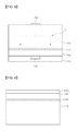
- Figure 1 is a sectional view of a light emitting device (LED) according to an embodiment.
- Figures 2 to 4 are sectional views illustrating a process of manufacturing the LED according to an embodiment.
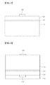
- Figure 5 is a sectional view of an LED according to another embodiment.
- Figures 6 to 8 are sectional views illustrating a process of manufacturing the LED according to another embodiment.
- Figure 9 is a sectional view of an LED package according to an embodiment.
- LEDs Light emitting devices
- Red and green LEDs may be used as light sources for electronic devices, including information communication devices.
- a gallium nitride (GaN) semiconductor has a high thermal stability and a wide band gap.
- the GaN semiconductor may be combined with other elements (e.g., In and Al) to fabricate a semiconductor layer emitting green, blue or white light, and its emitted wavelength may be controlled.
- LEDs including the GaN semiconductor may be used in high-power electronic devices.
- the LEDs may be a lateral type or a vertical type.
- an n-type electrode and a p-type electrode that inject current are disposed at an upper side and a lower side of the LEDs, respectively. Electrons and holes injected by the n-type electrode and the p-type electrode, respectively, flow into an active layer where they combine with each other to generate light that may be emitted.
- a portion of the light generated in the active layer may be reflected by the n-type electrode.
- the reflected light may be lost within the LED, thus light emission efficiency may be reduced.
- heat may be generated by re-absorbing the light reflected by the n-type electrode.
- a phenomenon of electron overflow may also occur below the n-type electrode which reduces the amount of emitted light.
- the electrons and holes may combine in a region outside the active layer which may generate additional heat. Current crowding may additionally deteriorate lifetime and reliability of the LED.
- FIG. 1 is a sectional view of a light emitting device (LED) according to an embodiment.
- a light emitting device (LED) may include a light emitting structure, a first current blocking layer 141, a second electrode 150, and a first electrode 160.
- the light emitting structure may include a second semiconductor layer 130 of a second conductivity type, an active layer 120, and a first semiconductor layer 110 of a first conductivity type.
- the first current blocking layer 141 may be disposed on the second semiconductor layer 130.
- the second electrode 150 may be disposed on the second semiconductor layer 130 and the first current blocking layer 141.
- the first electrode 160 may be disposed on the first semiconductor layer 110.
- the first current blocking layer 141 may be disposed in the second semiconductor layer 130, but is not limited thereto.
- the current blocking layer 141 may be disposed to induce a voltage drop that may adjust carrier distribution in the active layer 120.
- a doping concentration and thickness of a first conductive region that forms the current blocking layer 141 may be adjusted, or an ohmic contact with the second electrode may be adjusted to adjust the voltage drop in the active region defined below the first electrode, thereby reducing the electron overflow as well as improving current spreading and light emitting power.
- a method of manufacturing the LED according to an embodiment will be described with reference to Figures 2 to 4 .
- a first substrate is prepared.
- the first substrate may be a sapphire substrate, a SiC substrate, or other appropriate material based on the intended use of the material.
- a wet etching process may be performed on the first substrate to remove impurities on a surface of the first substrate.
- a first semiconductor layer 110 of a first conductivity type may be formed on the first substrate.
- an n-type GaN layer of the first semiconductor layer 110 of the first conductivity type may be formed using a chemical vapor deposition (CVD) process, a molecular beam epitaxy (MBE) process, a sputtering process, a hydride vapor phase epitaxial (HVPE) deposition process, or other appropriate processes.
- CVD chemical vapor deposition
- MBE molecular beam epitaxy
- HVPE hydride vapor phase epitaxial
- trimethylgallium gas (TMGa), ammonia gas (NH 3 ), nitrogen gas (N 2 ), silane gas (SiH 4 ), or other appropriate gases containing n-type impurities, such as silicon (Si) may be injected into a chamber to form the first semiconductor layer 110.
- An undoped semiconductor layer may be formed on the first substrate, and the first semiconductor layer 110 of the first conductivity type may be formed on the undoped semiconductor layer.
- an undoped GaN layer may be formed on the first substrate, then an n-type GaN layer may be formed on the undoped GaN layer to form the first semiconductor layer 110 of the first conductivity type.
- An active layer 120 may be formed on the first semiconductor layer 110.
- electrons injected through the first semiconductor layer 110 of the first conductivity type may combine when holes injected through the second semiconductor layer 130 of the second conductivity type to emit light having energy that is determined by an energy band of a material constituting the active layer (e.g., the light emitting layer).
- the active layer 120 may include at least one of a single quantum well structure, a multi-quantum well (MQW) structure, a quantum wire structure, and a quantum dot structure or other appropriate structures.
- the active layer 120 may have the multi-quantum well (MQW) structure of an InGaN/GaN structure formed by implanting a trimethyl gallium gas (TMGa), an ammonium gas (NH 3 ), a nitrogen gas (N 2 ), a Trimethyl indium gas (TMIn), or other appropriate gases.
- TMGa trimethyl gallium gas
- NH 3 ammonium gas
- N 2 nitrogen gas
- TIn Trimethyl indium gas
- the active layer 120 may have one or more structures of an InGaN/GaN structure, an InGaN/InGaN structure, an AIGaN/GaN structure, an InAlGaN/GaN structure, a GaAs/AlGaAs(InGaAs) structure, a GaP/AlGaP(InGaP) structure, or other appropriate structures.
- a second semiconductor layer 130 of the second conductivity type may be formed on the active layer 120.
- bis(ethylcyclopentadienyl) magnesium (EtCp 2 Mg) ⁇ Mg(C 2 H 5 C 5 H 4 ) 2 ⁇ containing p-type impurities, such as trimethyl gallium (TMGa) gas, ammonia (NH 3 ) gas, nitrogen (N 2 ) gas, magnesium (Mg), or other appropriate gases may be injected into the chamber to form a p-type GaN layer of the second semiconductor layer 130 of the second conductivity type, but is not limited thereto.
- TMGa trimethyl gallium
- NH 3 ammonia
- N 2 nitrogen
- Mg magnesium
- a first current blocking layer 141 may be formed on the second semiconductor layer 130 of the second conductivity type.
- the first current blocking layer 141 may include a semiconductor region of a conductivity type different than the second conductivity type.
- the first current blocking layer 141 may be a first conductive region or a non-conductive region that may be formed by performing a diffusion or ion implantation process on the second semiconductor layer 130 of the second conductivity type.
- the diffusion or ion implantation process may be performed using the first pattern as a mask.
- the first current blocking layer 141 may be formed at a position which spatially corresponds to a first electrode 160 that will be formed later.
- current blocking layer 141 may be formed to spatially overlap the first electrode 160.
- the spatial overlap may be a complete overlap or partial overlap.
- the current blocking layer 141 may be formed to cause a voltage drop when a constant voltage is applied.
- an energy barrier of the active layer 120 may increase in a region below the current blocking layer 141 to reduce carrier flow, thereby preventing electrons and holes from being combined with each other.
- an ohmic contact is provided between the second electrode 150 and the second semiconductor layer 130 other than where the current blocking layer 141 contacts the second semiconductor layer 130, thereby allowing carriers to smoothly flow through the ohmic contact.
- Such a structure may increase current spreading efficiency that may improve light extraction efficiency.
- the current blocking layer 141 may be formed to induce the voltage drop which adjusts carrier distribution in the active layer.
- a doping concentration and thickness of the first conductive region that forms the current blocking layer 141 may be adjusted, or an ohmic contact between the second electrode may be adjusted to adjust the voltage drop in the active region defined below the first electrode, thereby reducing the electron overflow as well as improving the current spreading and a light emitting power.
- the first pattern may be removed, and a second electrode 150 may be formed on the second semiconductor layer 130.
- the second electrode 150 may include an ohmic layer, a reflective layer, a coupling layer (e.g., junction layer), and a second substrate.
- the second electrode 150 may be formed of at least one of Titanium (Ti), Chrome (Cr), Nickel (Ni), Platinum (Pe), Gold (Av), Tungsten (N), or other appropriate materials, and a semiconductor substrate in which impurities are injected.
- the second electrode 150 may include the ohmic layer that may be formed by stacking a material, such as, a single metal, a metal alloy, a metal oxide, or other appropriate materials, in multiple layers to improve the efficiency of electron hole injection.
- the ohmic layer may be formed of at least one of ITO, IZO(In-ZnO), GZO(Ga-ZnO), AZO(Al-ZnO), AGZO(Al-Ga ZnO), IGZO(In-Ga ZnO), IrOx, RuOx, RuOx/ITO, Ni/IrOx/Au, Ni/IrOx/Au/ITO, Ni, Pt, Cr, Ti, Ag, or other appropriate materials.
- the second electrode 150 may include a metal layer containing Al, Ag, an alloy containing Al or Ag, or other appropriate materials.
- the material, such as Al or Ag may effectively reflect light generated at the active layer to improve light extraction efficiency, or optical efficiency, of the LED.
- the reflective layer may serve as the coupling layer, or the coupling layer may be formed using Ni or Au, or other appropriate materials.
- the second electrode 150 may further include the second substrate. However, when the first semiconductor layer 110 of the first conductivity type has a sufficient thickness of about 50 ⁇ m or greater, the second electrode 150 may, alternatively, not include the second substrate.
- the second substrate may be formed of a metal having good conductive properties, a metal alloy, a conductive semiconductor material, or other appropriate conductive material, to efficiently inject holes into the light emitting structure.
- the second substrate may be formed of one or more of copper (Cu), a Cu alloy, Si, molybdenum (Mo), SiGe, or other appropriate materials.
- the second substrate may be formed using an electrochemical metal deposition method, a bonding method using eutectic metals, or other appropriate methods.
- the first substrate may be removed to expose the first semiconductor layer 110 or the undoped semiconductor layer.
- the first substrate may be separated using a high power laser or removed using a chemical etching process.
- the first substrate may be also removed by performing a physical grinding process.
- the first electrode 160 may be formed on the first semiconductor layer 110.
- the first electrode 160 may be formed to spatially correspond to, the first current blocking layer 141.
- the first electrode 160 may be formed on first semiconductor layer 110 to overlap a region occupied by the first current blocking layer 141 on the second semiconductor layer 150.
- the first current blocking layer 141 may be placed in a region of the second semiconductor layer that spatially corresponds to, or at least partially overlaps, the first electrode 160, current C may not easily flow into the region above the first current blocking layer 141 may be reduced. Thus, current C may be diffused into a region outside the region above the first current blocking layer 141.
- the first current blocking layer 141 may include the first conductive region to serve as a current blocking layer 141. Thus, efficient current flow may be realized to improve reliability, and light absorption may be minimized to increase the amount of light that may be produced.
- the light extraction efficiency may be increased by including a light extraction structure.
- this embodiment may increase the light extraction efficiency by forming a photonic crystal or a roughness on the first semiconductor layer 110 of the first conductivity type, but is not limited thereto.
- the current blocking layer 141 may also be formed to efficiently adjust the current flow, thereby increasing the light extraction efficiency.
- the current blocking layer 141 may also improve the reliability due to the current spreading effect, and thereby increase a light output power.
- FIG. 5 is a sectional view of an LED according to another embodiment.
- An LED according to this embodiment may include a light emitting structure, a second current blocking layer 142, a second electrode 150, and a first electrode 160.
- the light emitting structure may include a second semiconductor layer 130 of a second conductivity type, an active layer 120, and a first semiconductor layer 110 of a first conductivity type.
- the second current blocking layer 142 may be disposed on the second semiconductor layer 130.
- the second electrode 150 may be disposed on the second semiconductor layer 130.
- the first electrode 160 may be disposed on the first semiconductor layer 110.
- the second current blocking layer 142 may be disposed in the second electrode 150, but is not limited thereto.
- the second current blocking layer 142 may be disposed on the second semiconductor layer 130, or alternatively, in the second electrode 150.
- a method of manufacturing the LED according to the second embodiment will be described with reference to Figures 6 to 8 .
- a first substrate (not shown) is prepared. Thereafter, a first semiconductor layer 110 of a first conductivity type, an active layer 120, and a second semiconductor layer 130 of a second conductivity type are formed on the first substrate.
- a second current blocking layer 142 may be formed on the second semiconductor layer 130.
- the second current blocking layer 142 may include a semiconductor region of a conductivity type different than the second conductivity type.
- the second current blocking layer 142 including a semiconductor region e.g., a first conductive layer doped with n-type impurities or a non-conductive layer, may be formed on the second semiconductor layer 130 of the second conductivity type.
- the first conductive layer or the non-conductive layer may be epitaxially grown, but is not limited thereto.
- a first pattern exposing a region in which the second current blocking layer 142 will be formed may be formed. Then, the first conductive layer 142a may be etched using the second pattern as an etch mask to form the second current blocking layer 142.
- the second current blocking layer 142 may be formed at a position that spatially corresponds to a first electrode 160 that will be formed later.
- the current blocking layer 142 may be formed to cause a voltage drop when a constant voltage is applied.
- an energy barrier of the active layer 120 may increase in a region below the current blocking layer 142, thereby decreasing carrier flow and preventing electron and hole combination at that region.
- a second electrode 150 (discussed in further detail below) has an ohmic contact with the second semiconductor layer 130 on surfaces other than where the current blocking layer 142 is positioned to allow carriers to smoothly flow through the ohmic contact.
- Such a structure may increase current spreading efficiency that may improve light extraction efficiency.
- the current blocking layer 142 may be formed to induce the voltage drop which adjusts carrier distribution in the active layer.
- a doping concentration and thickness of the first conductive region that forms the current blocking layer 142 may be adjusted, or an ohmic contact between the second electrode may be adjusted to adjust the voltage drop in the active region defined below the first electrode, thereby reducing the electron overflow as well as improving the current spreading and a light emitting power.
- the second pattern may be removed, and the second electrode 150 may be formed on the second semiconductor layer 130.
- the second electrode 150 may include an ohmic layer, a reflective layer, a coupling layer (e.g., junction layer), and a second substrate.
- the first substrate may be removed to expose the first semiconductor layer 110.
- the first electrode 160 may then be formed on the first semiconductor layer 110.
- the first electrode 160 may be positioned to spatially overlap the second current blocking layer 142.
- the second current blocking layer 142 may be formed on a region of the second semiconductor layer 130 that spatially corresponds below the first electrode 160, current C may not easily flow into the region above the second current blocking layer 142. Thus, current C may be diffused into a region outside the region above the second current blocking layer 142. Moreover, efficient current flow may be realized to improve reliability, and light absorption may be minimized increase the amount of light that may be produced.
- the current blocking layer 142 may also be formed to vary the efficiency of current flow, thereby increasing the light extraction efficiency. The current blocking layer may also improve the reliability due to the current spreading effect, and thereby increase a light output power.
- FIG 9 is a sectional view of an LED package according to an embodiment.
- an LED package according to an embodiment includes a body 200, a third electrode layer 210 and a fourth electrode layer 220 disposed in the body 200, an LED 100 disposed in the body 200 and electrically connected to the third electrode layer 210 and the fourth electrode layer 220, and a molding member 400 surrounding the LED 100.
- the body 200 may be formed of a silicon material, a synthetic resin material, a metal material, or other appropriate materials.
- a sloped surface may be disposed around the LED 100.
- the third electrode layer 210 and the fourth electrode layer 220 are electrically separated from each other, and may supply power to the LED 100. Also, the third electrode layer 210 and the fourth electrode layer 220 may reflect light generated in the LED 100 to improve light efficiency. In addition, the third electrode layer 210 and the fourth electrode layer 220 may transfer heat generated in the LED 100 to the body 200.
- LED 100 may be a vertical type LED as illustrated in Figure 1 , but is not limited thereto.
- a lateral type LED may be applicable as the LED 100.
- the LED 100 may be disposed on the body 200 or on the third electrode layer 210 or the fourth electrode layer 220.
- the LED 100 may be electrically connected to the third electrode layer 210 and/or the fourth electrode layer 220 through a wire 300.
- a vertical type LED 100 for example, one wire 300 may be used, but is not limited thereto.
- the LED 100 includes the lateral type LED, two wires may be used.
- the LED 100 includes a flip-chip type LED, the wire 300 may not be needed.
- the molding member 400 may surround the LED 100 to protect the LED 100.
- a phosphor may be also contained in the molding member 400 to vary a wavelength of light emitted from the LED 100.
- the current blocking layer may be formed to efficiently adjust the current flow, thereby increasing the light extraction efficiency.
- the current blocking layer 142 may be also formed to improve the reliability due to the current spreading effect and increase the light output power.
- a plurality of LED packages are arranged in an array on a substrate.
- a light guide panel, a prism sheet, and a diffusion sheet, which are optical members, may be disposed on an optical path of the LED package.
- the LED package, the substrate, and the optical member may serve as a light unit.
- a display device, an indication device, and a light system which may include the LED or the LED package disclosed in the above-described embodiments, may be realized.
- the lighting system including a light emitting module including the LED package may be used as a lamp or streetlight.
- Embodiments provide a light emitting device that can improve current crowding and light extraction efficiency, a light emitting device package and a lighting system including the same.
- a light emitting device comprises: a light emitting structure comprising a second conductive type semiconductor layer, an active layer on the second conductive type semiconductor layer, and a first conductive type semiconductor layer on the active layer; a current blocking layer below the second conductive type semiconductor layer; a second electrode below the second conductive type semiconductor layer; and a first electrode on the first conductive type semiconductor layer, wherein the current blocking layer comprises a non second conductive region.
- an LED package comprises the LED; and a package body in which the LED is disposed.
- a lighting system comprises a light emitting module comprising the LED package.
- a light emitting device comprises a light emitting structure comprising a first semiconductor layer of a first conductivity type, an active layer adjacent the first semiconductor layer, and a second semiconductor layer of a second conductivity type adjacent the active layer; a current blocking layer adjacent to the second semiconductor layer; a first electrode adjacent the first semiconductor layer; and a second electrode adjacent the second semiconductor layer; and wherein the current blocking layer comprises a semiconductor region.
- the LED includes the current blocking layer comprising a GaN semiconductor layer; wherein the semiconductor region has a first conductivity type; wherein the semiconductor region is an undoped semiconductor region; wherein the semiconductor region is a lightly doped semiconductor region; wherein the first electrode spatially overlaps at least portion of the current blocking layer; wherein the current blocking layer is disposed in the second semiconductor layer; wherein the current blocking layer is disposed in the second electrode; and wherein an ohmic contact is provided between the second semiconductor layer and the second electrode other than where the current blocking layer contacts the second semiconductor layer.
- a method of manufacturing a light emitting device comprises forming an active layer on a first semiconductor layer of a first conductivity type; forming a second semiconductor layer of a second conductivity type on the active layer; forming a current blocking layer including a semiconductor region on the second semiconductor layer; forming a first electrode on the first semiconductor layer, wherein the first electrode is positioned to spatially overlap the current blocking layer formed on the second semiconductor layer; and forming a second electrode on the second semiconductor layer and the semiconductor region.
- the method further includes the step of forming the current blocking layer comprising placing a first mask on a surface of the second semiconductor layer; and doping the surface of the second semiconductor layer using the first mask to form the semiconductor region of a conductivity type different than that of the second semiconductor layer; wherein the conductivity type of the semiconductor region is the first conductivity type; and wherein the semiconductor region is at least one of an undoped or a lightly doped semiconductor region.
- the method further includes the step of forming the current blocking layer comprising forming a semiconductor region on top of the second semiconductor layer; wherein the step of forming the second electrode includes forming an ohmic contact between the second electrode and the second semiconductor layer other than where the current blocking layer contacts the second semiconductor layer; wherein the step of forming the current blocking layer further comprises adjusting a thickness of the current blocking layer to control a carrier distribution in the active layer that is spatially overlapped by the current blocking layer; wherein the step of forming the current blocking layer further comprises adjusting a doping concentration of the current blocking layer to control a carrier distribution in the active layer that is spatially overlapped by the current blocking layer; and wherein the step of forming the second electrode further comprises adjusting the ohmic contact of the second electrode to vary a voltage drop in an active region below the first electrode, wherein the voltage drop controls a carrier distribution in the active layer that is spatially overlapped by the current blocking layer.
- a layer (or film) is referred to as being 'on' another layer or substrate, it can be directly on another layer or substrate, or intervening layers may also be present. Further, it will be understood that when a layer is referred to as being 'under' another layer, it can be directly under another layer, and one or more intervening layers may also be present. In addition, it will also be understood that when a layer is referred to as being 'between' two layers, it can be the only layer between the two layers, or one or more intervening layers may also be present.
- any reference in this specification to "one embodiment,” “an embodiment,” “example embodiment,” etc. means that a particular feature, structure, or characteristic described in connection with the embodiment is included in at least one embodiment of the invention.
- the appearances of such phrases in various places in the specification are not necessarily all referring to the same embodiment.
Landscapes
- Led Devices (AREA)
Abstract
Description
- A light emitting device, package, and system are disclosed herein.
- A light emitting device, a light emitting device package, and a lighting system including the same are known. However, they suffer from various disadvantages.
- The embodiments will be described in detail with reference to the following drawings in which like reference numerals refer to like elements, wherein:
-
Figure 1 is a sectional view of a light emitting device (LED) according to an embodiment. -
Figures 2 to 4 are sectional views illustrating a process of manufacturing the LED according to an embodiment. -
Figure 5 is a sectional view of an LED according to another embodiment. -
Figures 6 to 8 are sectional views illustrating a process of manufacturing the LED according to another embodiment. -
Figure 9 is a sectional view of an LED package according to an embodiment. - Light emitting devices (LEDs) are semiconductor devices that convert a current into light. Red and green LEDs may be used as light sources for electronic devices, including information communication devices. For example, a gallium nitride (GaN) semiconductor has a high thermal stability and a wide band gap. The GaN semiconductor may be combined with other elements (e.g., In and Al) to fabricate a semiconductor layer emitting green, blue or white light, and its emitted wavelength may be controlled. Thus, LEDs including the GaN semiconductor may be used in high-power electronic devices.
- The LEDs may be a lateral type or a vertical type. In vertical LEDs, an n-type electrode and a p-type electrode that inject current are disposed at an upper side and a lower side of the LEDs, respectively. Electrons and holes injected by the n-type electrode and the p-type electrode, respectively, flow into an active layer where they combine with each other to generate light that may be emitted.
- A portion of the light generated in the active layer may be reflected by the n-type electrode. Thus, the reflected light may be lost within the LED, thus light emission efficiency may be reduced. Further, heat may be generated by re-absorbing the light reflected by the n-type electrode. A phenomenon of electron overflow may also occur below the n-type electrode which reduces the amount of emitted light. The electrons and holes may combine in a region outside the active layer which may generate additional heat. Current crowding may additionally deteriorate lifetime and reliability of the LED.
-
Figure 1 is a sectional view of a light emitting device (LED) according to an embodiment. A light emitting device (LED) according to this embodiment may include a light emitting structure, a firstcurrent blocking layer 141, asecond electrode 150, and afirst electrode 160. The light emitting structure may include asecond semiconductor layer 130 of a second conductivity type, anactive layer 120, and afirst semiconductor layer 110 of a first conductivity type. The firstcurrent blocking layer 141 may be disposed on thesecond semiconductor layer 130. Thesecond electrode 150 may be disposed on thesecond semiconductor layer 130 and the firstcurrent blocking layer 141. Thefirst electrode 160 may be disposed on thefirst semiconductor layer 110. - The first
current blocking layer 141 may be disposed in thesecond semiconductor layer 130, but is not limited thereto. Thecurrent blocking layer 141 may be disposed to induce a voltage drop that may adjust carrier distribution in theactive layer 120. For example, a doping concentration and thickness of a first conductive region that forms thecurrent blocking layer 141 may be adjusted, or an ohmic contact with the second electrode may be adjusted to adjust the voltage drop in the active region defined below the first electrode, thereby reducing the electron overflow as well as improving current spreading and light emitting power. - A method of manufacturing the LED according to an embodiment will be described with reference to
Figures 2 to 4 . A first substrate is prepared. The first substrate may be a sapphire substrate, a SiC substrate, or other appropriate material based on the intended use of the material. A wet etching process may be performed on the first substrate to remove impurities on a surface of the first substrate. - A
first semiconductor layer 110 of a first conductivity type may be formed on the first substrate. For example, an n-type GaN layer of thefirst semiconductor layer 110 of the first conductivity type may be formed using a chemical vapor deposition (CVD) process, a molecular beam epitaxy (MBE) process, a sputtering process, a hydride vapor phase epitaxial (HVPE) deposition process, or other appropriate processes. Also, trimethylgallium gas (TMGa), ammonia gas (NH3), nitrogen gas (N2), silane gas (SiH4), or other appropriate gases containing n-type impurities, such as silicon (Si), may be injected into a chamber to form thefirst semiconductor layer 110. - An undoped semiconductor layer may be formed on the first substrate, and the
first semiconductor layer 110 of the first conductivity type may be formed on the undoped semiconductor layer. For example, an undoped GaN layer may be formed on the first substrate, then an n-type GaN layer may be formed on the undoped GaN layer to form thefirst semiconductor layer 110 of the first conductivity type. - An
active layer 120 may be formed on thefirst semiconductor layer 110. In theactive layer 120, electrons injected through thefirst semiconductor layer 110 of the first conductivity type may combine when holes injected through thesecond semiconductor layer 130 of the second conductivity type to emit light having energy that is determined by an energy band of a material constituting the active layer (e.g., the light emitting layer). - The
active layer 120 may include at least one of a single quantum well structure, a multi-quantum well (MQW) structure, a quantum wire structure, and a quantum dot structure or other appropriate structures. For example, theactive layer 120 may have the multi-quantum well (MQW) structure of an InGaN/GaN structure formed by implanting a trimethyl gallium gas (TMGa), an ammonium gas (NH3), a nitrogen gas (N2), a Trimethyl indium gas (TMIn), or other appropriate gases. Theactive layer 120 may have one or more structures of an InGaN/GaN structure, an InGaN/InGaN structure, an AIGaN/GaN structure, an InAlGaN/GaN structure, a GaAs/AlGaAs(InGaAs) structure, a GaP/AlGaP(InGaP) structure, or other appropriate structures. - A
second semiconductor layer 130 of the second conductivity type may be formed on theactive layer 120. For example, bis(ethylcyclopentadienyl) magnesium (EtCp2Mg){Mg(C2H5C5H4)2} containing p-type impurities, such as trimethyl gallium (TMGa) gas, ammonia (NH3) gas, nitrogen (N2) gas, magnesium (Mg), or other appropriate gases may be injected into the chamber to form a p-type GaN layer of thesecond semiconductor layer 130 of the second conductivity type, but is not limited thereto. - Referring to
Figure 3 , a firstcurrent blocking layer 141 may be formed on thesecond semiconductor layer 130 of the second conductivity type. The firstcurrent blocking layer 141 may include a semiconductor region of a conductivity type different than the second conductivity type. For example, the firstcurrent blocking layer 141 may be a first conductive region or a non-conductive region that may be formed by performing a diffusion or ion implantation process on thesecond semiconductor layer 130 of the second conductivity type. A first pattern exposing a region in which the firstcurrent blocking layer 141 may be formed on thesecond semiconductor layer 130. The diffusion or ion implantation process may be performed using the first pattern as a mask. The firstcurrent blocking layer 141 may be formed at a position which spatially corresponds to afirst electrode 160 that will be formed later. For example,current blocking layer 141 may be formed to spatially overlap thefirst electrode 160. The spatial overlap may be a complete overlap or partial overlap. - The
current blocking layer 141 may be formed to cause a voltage drop when a constant voltage is applied. Thus, an energy barrier of theactive layer 120 may increase in a region below thecurrent blocking layer 141 to reduce carrier flow, thereby preventing electrons and holes from being combined with each other. Referring now toFigure 4 , an ohmic contact is provided between thesecond electrode 150 and thesecond semiconductor layer 130 other than where thecurrent blocking layer 141 contacts thesecond semiconductor layer 130, thereby allowing carriers to smoothly flow through the ohmic contact. Such a structure may increase current spreading efficiency that may improve light extraction efficiency. - For example, the
current blocking layer 141 may be formed to induce the voltage drop which adjusts carrier distribution in the active layer. In particular, a doping concentration and thickness of the first conductive region that forms thecurrent blocking layer 141 may be adjusted, or an ohmic contact between the second electrode may be adjusted to adjust the voltage drop in the active region defined below the first electrode, thereby reducing the electron overflow as well as improving the current spreading and a light emitting power. - As shown in
Figure 4 , the first pattern may be removed, and asecond electrode 150 may be formed on thesecond semiconductor layer 130. Thesecond electrode 150 may include an ohmic layer, a reflective layer, a coupling layer (e.g., junction layer), and a second substrate. Thesecond electrode 150 may be formed of at least one of Titanium (Ti), Chrome (Cr), Nickel (Ni), Platinum (Pe), Gold (Av), Tungsten (N), or other appropriate materials, and a semiconductor substrate in which impurities are injected. - The
second electrode 150 may include the ohmic layer that may be formed by stacking a material, such as, a single metal, a metal alloy, a metal oxide, or other appropriate materials, in multiple layers to improve the efficiency of electron hole injection. The ohmic layer may be formed of at least one of ITO, IZO(In-ZnO), GZO(Ga-ZnO), AZO(Al-ZnO), AGZO(Al-Ga ZnO), IGZO(In-Ga ZnO), IrOx, RuOx, RuOx/ITO, Ni/IrOx/Au, Ni/IrOx/Au/ITO, Ni, Pt, Cr, Ti, Ag, or other appropriate materials. - When the
second electrode 150 includes the reflective layer, thesecond electrode 150 may include a metal layer containing Al, Ag, an alloy containing Al or Ag, or other appropriate materials. The material, such as Al or Ag, may effectively reflect light generated at the active layer to improve light extraction efficiency, or optical efficiency, of the LED. When thesecond electrode 150 further includes the coupling layer, the reflective layer may serve as the coupling layer, or the coupling layer may be formed using Ni or Au, or other appropriate materials. - The
second electrode 150 may further include the second substrate. However, when thefirst semiconductor layer 110 of the first conductivity type has a sufficient thickness of about 50 µm or greater, thesecond electrode 150 may, alternatively, not include the second substrate. The second substrate may be formed of a metal having good conductive properties, a metal alloy, a conductive semiconductor material, or other appropriate conductive material, to efficiently inject holes into the light emitting structure. For example, the second substrate may be formed of one or more of copper (Cu), a Cu alloy, Si, molybdenum (Mo), SiGe, or other appropriate materials. The second substrate may be formed using an electrochemical metal deposition method, a bonding method using eutectic metals, or other appropriate methods. - The first substrate may be removed to expose the
first semiconductor layer 110 or the undoped semiconductor layer. The first substrate may be separated using a high power laser or removed using a chemical etching process. The first substrate may be also removed by performing a physical grinding process. Thereafter, thefirst electrode 160 may be formed on thefirst semiconductor layer 110. Thefirst electrode 160 may be formed to spatially correspond to, the firstcurrent blocking layer 141. For example, thefirst electrode 160 may be formed onfirst semiconductor layer 110 to overlap a region occupied by the firstcurrent blocking layer 141 on thesecond semiconductor layer 150. - Since the first
current blocking layer 141 may be placed in a region of the second semiconductor layer that spatially corresponds to, or at least partially overlaps, thefirst electrode 160, current C may not easily flow into the region above the firstcurrent blocking layer 141 may be reduced. Thus, current C may be diffused into a region outside the region above the firstcurrent blocking layer 141. For example, the firstcurrent blocking layer 141 may include the first conductive region to serve as acurrent blocking layer 141. Thus, efficient current flow may be realized to improve reliability, and light absorption may be minimized to increase the amount of light that may be produced. - Further, the light extraction efficiency may be increased by including a light extraction structure. For example, this embodiment may increase the light extraction efficiency by forming a photonic crystal or a roughness on the
first semiconductor layer 110 of the first conductivity type, but is not limited thereto. Thecurrent blocking layer 141 may also be formed to efficiently adjust the current flow, thereby increasing the light extraction efficiency. Thecurrent blocking layer 141 may also improve the reliability due to the current spreading effect, and thereby increase a light output power. -
Figure 5 is a sectional view of an LED according to another embodiment. An LED according to this embodiment may include a light emitting structure, a secondcurrent blocking layer 142, asecond electrode 150, and afirst electrode 160. The light emitting structure may include asecond semiconductor layer 130 of a second conductivity type, anactive layer 120, and afirst semiconductor layer 110 of a first conductivity type. The secondcurrent blocking layer 142 may be disposed on thesecond semiconductor layer 130. Thesecond electrode 150 may be disposed on thesecond semiconductor layer 130. Thefirst electrode 160 may be disposed on thefirst semiconductor layer 110. In this embodiment, the secondcurrent blocking layer 142 may be disposed in thesecond electrode 150, but is not limited thereto. - This embodiment may adopt the technical features of the embodiments discussed previously. Thus, where possible, the disclosure of this embodiment will be directed to the differences to the previous embodiments. In this embodiment, the second
current blocking layer 142 may be disposed on thesecond semiconductor layer 130, or alternatively, in thesecond electrode 150. - A method of manufacturing the LED according to the second embodiment will be described with reference to
Figures 6 to 8 . Referring toFigure 6 , a first substrate (not shown) is prepared. Thereafter, afirst semiconductor layer 110 of a first conductivity type, anactive layer 120, and asecond semiconductor layer 130 of a second conductivity type are formed on the first substrate. A secondcurrent blocking layer 142 may be formed on thesecond semiconductor layer 130. In this embodiment, the secondcurrent blocking layer 142 may include a semiconductor region of a conductivity type different than the second conductivity type. - In this embodiment, the second
current blocking layer 142 including a semiconductor region, e.g., a first conductive layer doped with n-type impurities or a non-conductive layer, may be formed on thesecond semiconductor layer 130 of the second conductivity type. For example, the first conductive layer or the non-conductive layer may be epitaxially grown, but is not limited thereto. - Referring to
Figure 7 , a first pattern exposing a region in which the secondcurrent blocking layer 142 will be formed may be formed. Then, the first conductive layer 142a may be etched using the second pattern as an etch mask to form the secondcurrent blocking layer 142. The secondcurrent blocking layer 142 may be formed at a position that spatially corresponds to afirst electrode 160 that will be formed later. - The
current blocking layer 142 may be formed to cause a voltage drop when a constant voltage is applied. Thus, an energy barrier of theactive layer 120 may increase in a region below thecurrent blocking layer 142, thereby decreasing carrier flow and preventing electron and hole combination at that region. Further, a second electrode 150 (discussed in further detail below) has an ohmic contact with thesecond semiconductor layer 130 on surfaces other than where thecurrent blocking layer 142 is positioned to allow carriers to smoothly flow through the ohmic contact. Such a structure may increase current spreading efficiency that may improve light extraction efficiency. - For example, the
current blocking layer 142 may be formed to induce the voltage drop which adjusts carrier distribution in the active layer. In particular, a doping concentration and thickness of the first conductive region that forms thecurrent blocking layer 142 may be adjusted, or an ohmic contact between the second electrode may be adjusted to adjust the voltage drop in the active region defined below the first electrode, thereby reducing the electron overflow as well as improving the current spreading and a light emitting power. - As shown in
Figure 8 , the second pattern may be removed, and thesecond electrode 150 may be formed on thesecond semiconductor layer 130. Thesecond electrode 150 may include an ohmic layer, a reflective layer, a coupling layer (e.g., junction layer), and a second substrate. The first substrate may be removed to expose thefirst semiconductor layer 110. Thefirst electrode 160 may then be formed on thefirst semiconductor layer 110. Thefirst electrode 160 may be positioned to spatially overlap the secondcurrent blocking layer 142. - Since the second
current blocking layer 142 may be formed on a region of thesecond semiconductor layer 130 that spatially corresponds below thefirst electrode 160, current C may not easily flow into the region above the secondcurrent blocking layer 142. Thus, current C may be diffused into a region outside the region above the secondcurrent blocking layer 142. Moreover, efficient current flow may be realized to improve reliability, and light absorption may be minimized increase the amount of light that may be produced. Thecurrent blocking layer 142 may also be formed to vary the efficiency of current flow, thereby increasing the light extraction efficiency. The current blocking layer may also improve the reliability due to the current spreading effect, and thereby increase a light output power. -
Figure 9 is a sectional view of an LED package according to an embodiment. Referring toFigure 9 , an LED package according to an embodiment includes abody 200, athird electrode layer 210 and afourth electrode layer 220 disposed in thebody 200, anLED 100 disposed in thebody 200 and electrically connected to thethird electrode layer 210 and thefourth electrode layer 220, and amolding member 400 surrounding theLED 100. - The
body 200 may be formed of a silicon material, a synthetic resin material, a metal material, or other appropriate materials. A sloped surface may be disposed around theLED 100. - The
third electrode layer 210 and thefourth electrode layer 220 are electrically separated from each other, and may supply power to theLED 100. Also, thethird electrode layer 210 and thefourth electrode layer 220 may reflect light generated in theLED 100 to improve light efficiency. In addition, thethird electrode layer 210 and thefourth electrode layer 220 may transfer heat generated in theLED 100 to thebody 200. -
LED 100 may be a vertical type LED as illustrated inFigure 1 , but is not limited thereto. For example, a lateral type LED may be applicable as theLED 100. TheLED 100 may be disposed on thebody 200 or on thethird electrode layer 210 or thefourth electrode layer 220. - The
LED 100 may be electrically connected to thethird electrode layer 210 and/or thefourth electrode layer 220 through awire 300. In this embodiment, if avertical type LED 100 is used, for example, onewire 300 may be used, but is not limited thereto. Further, when theLED 100 includes the lateral type LED, two wires may be used. Also, when theLED 100 includes a flip-chip type LED, thewire 300 may not be needed. Further, themolding member 400 may surround theLED 100 to protect theLED 100. A phosphor may be also contained in themolding member 400 to vary a wavelength of light emitted from theLED 100. - The current blocking layer may be formed to efficiently adjust the current flow, thereby increasing the light extraction efficiency. The
current blocking layer 142 may be also formed to improve the reliability due to the current spreading effect and increase the light output power. - In the LED package according to an embodiment, a plurality of LED packages are arranged in an array on a substrate. A light guide panel, a prism sheet, and a diffusion sheet, which are optical members, may be disposed on an optical path of the LED package. The LED package, the substrate, and the optical member may serve as a light unit. In another embodiment, a display device, an indication device, and a light system, which may include the LED or the LED package disclosed in the above-described embodiments, may be realized. For example, the lighting system, including a light emitting module including the LED package may be used as a lamp or streetlight.
- Embodiments provide a light emitting device that can improve current crowding and light extraction efficiency, a light emitting device package and a lighting system including the same.
- In one embodiment, a light emitting device (LED) comprises: a light emitting structure comprising a second conductive type semiconductor layer, an active layer on the second conductive type semiconductor layer, and a first conductive type semiconductor layer on the active layer; a current blocking layer below the second conductive type semiconductor layer; a second electrode below the second conductive type semiconductor layer; and a first electrode on the first conductive type semiconductor layer, wherein the current blocking layer comprises a non second conductive region.
- In another embodiment, an LED package comprises the LED; and a package body in which the LED is disposed.
- In further another embodiment, a lighting system comprises a light emitting module comprising the LED package.
- A light emitting device (LED) comprises a light emitting structure comprising a first semiconductor layer of a first conductivity type, an active layer adjacent the first semiconductor layer, and a second semiconductor layer of a second conductivity type adjacent the active layer; a current blocking layer adjacent to the second semiconductor layer; a first electrode adjacent the first semiconductor layer; and a second electrode adjacent the second semiconductor layer; and wherein the current blocking layer comprises a semiconductor region.
- The LED includes the current blocking layer comprising a GaN semiconductor layer; wherein the semiconductor region has a first conductivity type; wherein the semiconductor region is an undoped semiconductor region; wherein the semiconductor region is a lightly doped semiconductor region; wherein the first electrode spatially overlaps at least portion of the current blocking layer; wherein the current blocking layer is disposed in the second semiconductor layer; wherein the current blocking layer is disposed in the second electrode; and wherein an ohmic contact is provided between the second semiconductor layer and the second electrode other than where the current blocking layer contacts the second semiconductor layer.
- A method of manufacturing a light emitting device (LED) comprises forming an active layer on a first semiconductor layer of a first conductivity type; forming a second semiconductor layer of a second conductivity type on the active layer; forming a current blocking layer including a semiconductor region on the second semiconductor layer; forming a first electrode on the first semiconductor layer, wherein the first electrode is positioned to spatially overlap the current blocking layer formed on the second semiconductor layer; and forming a second electrode on the second semiconductor layer and the semiconductor region.
- The method further includes the step of forming the current blocking layer comprising placing a first mask on a surface of the second semiconductor layer; and doping the surface of the second semiconductor layer using the first mask to form the semiconductor region of a conductivity type different than that of the second semiconductor layer; wherein the conductivity type of the semiconductor region is the first conductivity type; and wherein the semiconductor region is at least one of an undoped or a lightly doped semiconductor region.
- The method further includes the step of forming the current blocking layer comprising forming a semiconductor region on top of the second semiconductor layer; wherein the step of forming the second electrode includes forming an ohmic contact between the second electrode and the second semiconductor layer other than where the current blocking layer contacts the second semiconductor layer; wherein the step of forming the current blocking layer further comprises adjusting a thickness of the current blocking layer to control a carrier distribution in the active layer that is spatially overlapped by the current blocking layer; wherein the step of forming the current blocking layer further comprises adjusting a doping concentration of the current blocking layer to control a carrier distribution in the active layer that is spatially overlapped by the current blocking layer; and wherein the step of forming the second electrode further comprises adjusting the ohmic contact of the second electrode to vary a voltage drop in an active region below the first electrode, wherein the voltage drop controls a carrier distribution in the active layer that is spatially overlapped by the current blocking layer.
- In the descriptions of embodiments, it will be understood that when a layer (or film) is referred to as being 'on' another layer or substrate, it can be directly on another layer or substrate, or intervening layers may also be present. Further, it will be understood that when a layer is referred to as being 'under' another layer, it can be directly under another layer, and one or more intervening layers may also be present. In addition, it will also be understood that when a layer is referred to as being 'between' two layers, it can be the only layer between the two layers, or one or more intervening layers may also be present.
- Any reference in this specification to "one embodiment," "an embodiment," "example embodiment," etc., means that a particular feature, structure, or characteristic described in connection with the embodiment is included in at least one embodiment of the invention. The appearances of such phrases in various places in the specification are not necessarily all referring to the same embodiment. Further, when a particular feature, structure, or characteristic is described in connection with any embodiment, it is submitted that it is within the purview of one skilled in the art to effect such feature, structure, or characteristic in connection with other ones of the embodiments.
- Although embodiments have been described with reference to a number of illustrative embodiments thereof, it should be understood that numerous other modifications and embodiments can be devised by those skilled in the art that will fall within the spirit and scope of the principles of this disclosure. More particularly, various variations and modifications are possible in the component parts and/or arrangements of the subject combination arrangement within the scope of the disclosure, the drawings and the appended claims. In addition to variations and modifications in the component parts and/or arrangements, alternative uses will also be apparent to those skilled in the art.
Claims (15)
- A light emitting device (LED) comprising:a light emitting structure comprising a first semiconductor layer of a first conductivity type, an active layer adjacent the first semiconductor layer, and a second semiconductor layer of a second conductivity type adjacent the active layer;a current blocking layer adjacent to the second semiconductor layer;a first electrode adjacent the first semiconductor layer; anda second electrode adjacent the second semiconductor layer; andwherein the current blocking layer comprises a semiconductor region.
- The LED of claim 1, wherein the current blocking layer comprises a GaN semiconductor layer.
- The LED of claim 1, wherein the semiconductor region has a first conductivity type.
- The LED of claim 1, wherein the semiconductor region is an undoped semiconductor region.
- The LED of claim 1, wherein the semiconductor region is a lightly doped semiconductor region.
- The LED of claim 1, wherein the first electrode spatially overlaps at least portion of the current blocking layer.
- The LED of claim 1, wherein the current blocking layer is disposed in the second semiconductor layer.
- The LED of claim 1, wherein the current blocking layer is disposed in the second electrode.
- The LED of claim 1, wherein an ohmic contact is provided between the second semiconductor layer and the second electrode other than where the current blocking layer contacts the second semiconductor layer.
- An LED package comprising:the LED of claim 1; anda package body in which the LED is disposed.
- A lighting system comprising a light emitting module comprising the LED package of claim 10.
- A method of manufacturing a light emitting device (LED), comprising
forming an active layer on a first semiconductor layer of a first conductivity type;
forming a second semiconductor layer of a second conductivity type on the active layer;
forming a current blocking layer including a semiconductor region on the second semiconductor layer;
forming a first electrode on the first semiconductor layer, wherein the first electrode is positioned to spatially overlap the current blocking layer formed on the second semiconductor layer; and
forming a second electrode on the second semiconductor layer and the semiconductor region. - The method of claim 12, wherein the step of forming the current blocking layer comprises:placing a first mask on a surface of the second semiconductor layer; anddoping the surface of the second semiconductor layer using the first mask to form the semiconductor region of a conductivity type different than that of the second semiconductor layer.
- The method of claim 12, wherein the step of forming the current blocking layer comprises forming a semiconductor region on top of the second semiconductor layer.
- The method of claim 12, wherein the step of forming the current blocking layer further comprises adjusting a doping concentration of the current blocking layer to control a carrier distribution in the active layer that is spatially overlapped by the current blocking layer.
Applications Claiming Priority (1)
| Application Number | Priority Date | Filing Date | Title |
|---|---|---|---|
| KR1020090041971A KR20100122998A (en) | 2009-05-14 | 2009-05-14 | Light emitting device and method for fabricating the same |
Publications (1)
| Publication Number | Publication Date |
|---|---|
| EP2251916A1 true EP2251916A1 (en) | 2010-11-17 |
Family
ID=42671749
Family Applications (1)
| Application Number | Title | Priority Date | Filing Date |
|---|---|---|---|
| EP10162697A Ceased EP2251916A1 (en) | 2009-05-14 | 2010-05-12 | Light emitting device, light emitting device package and lighting system including the same |
Country Status (4)
| Country | Link |
|---|---|
| US (1) | US20100308339A1 (en) |
| EP (1) | EP2251916A1 (en) |
| KR (1) | KR20100122998A (en) |
| CN (1) | CN101887933A (en) |
Families Citing this family (7)
| Publication number | Priority date | Publication date | Assignee | Title |
|---|---|---|---|---|
| KR100969100B1 (en) * | 2010-02-12 | 2010-07-09 | 엘지이노텍 주식회사 | Light emitting device, manufacturing method and light emitting device package |
| CN102214743A (en) * | 2011-06-09 | 2011-10-12 | 中国科学院半导体研究所 | Method for manufacturing current blocking layer of gallium nitride-based light-emitting diode (LED) |
| CN102299218B (en) * | 2011-08-24 | 2015-04-01 | 上海蓝光科技有限公司 | Light emitting diode and manufacturing method thereof |
| KR101865934B1 (en) * | 2011-12-16 | 2018-06-11 | 엘지이노텍 주식회사 | Light emitting device, light emitting device package, and light unit |
| CN103311382B (en) * | 2012-03-14 | 2016-04-13 | 上海博恩世通光电股份有限公司 | A kind of LED chip and preparation method thereof |
| CN105428483B (en) * | 2015-12-21 | 2018-04-10 | 天津三安光电有限公司 | Light emitting diode and preparation method thereof |
| CN106935151B (en) * | 2017-02-28 | 2019-04-26 | 郑清团 | Wafer-level micro-nano-scale semiconductor LED display and preparation method thereof |
Citations (6)
| Publication number | Priority date | Publication date | Assignee | Title |
|---|---|---|---|---|
| US5814839A (en) * | 1995-02-16 | 1998-09-29 | Sharp Kabushiki Kaisha | Semiconductor light-emitting device having a current adjusting layer and a uneven shape light emitting region, and method for producing same |
| DE19745723A1 (en) * | 1997-10-16 | 1998-12-10 | Telefunken Microelectron | Light emitting semiconductor device especially LED |
| US6420198B1 (en) * | 1996-12-24 | 2002-07-16 | Nec Corporation | Gallium nitride based compound semiconductor laser and method of forming the same |
| US20070145391A1 (en) * | 2005-12-26 | 2007-06-28 | Samsung Electro-Mechanics Co., Ltd. | Vertical type nitride semiconductor light emitting device and method of manufacturing the same |
| DE102006034847A1 (en) * | 2006-04-27 | 2007-10-31 | Osram Opto Semiconductors Gmbh | Opto-electronic semiconductor chip e.g. light emitting diode chip, has contact layer, where electrical contact resistance of contact layer to connection layer is smaller than contact layer to barrier layer |
| US20080217635A1 (en) * | 2004-06-30 | 2008-09-11 | David Todd Emerson | Light emitting devices having current reducing structures and methods of forming light emitting devices having current reducing structures |
Family Cites Families (6)
| Publication number | Priority date | Publication date | Assignee | Title |
|---|---|---|---|---|
| US7339255B2 (en) * | 2004-08-24 | 2008-03-04 | Kabushiki Kaisha Toshiba | Semiconductor device having bidirectionally inclined toward <1-100> and <11-20> relative to {0001} crystal planes |
| KR20060034456A (en) * | 2004-10-19 | 2006-04-24 | 삼성전자주식회사 | Semiconductor laser diode and manufacturing method thereof |
| US8100567B2 (en) * | 2005-10-19 | 2012-01-24 | Rambus International Ltd. | Light-emitting devices and related systems |
| DE112006002927B4 (en) * | 2006-01-09 | 2010-06-02 | Seoul Opto Device Co. Ltd., Ansan | Light-emitting diode with ITO layer and method for producing such |
| JP5430826B2 (en) * | 2006-03-08 | 2014-03-05 | シャープ株式会社 | Nitride semiconductor laser device |
| TWI363440B (en) * | 2007-11-01 | 2012-05-01 | Univ Nat Taiwan | Light-emitting device, light-emitting diode and method for forming a light-emitting device |
-
2009
- 2009-05-14 KR KR1020090041971A patent/KR20100122998A/en not_active Ceased
-
2010
- 2010-05-12 US US12/778,537 patent/US20100308339A1/en not_active Abandoned
- 2010-05-12 EP EP10162697A patent/EP2251916A1/en not_active Ceased
- 2010-05-14 CN CN2010101805404A patent/CN101887933A/en active Pending
Patent Citations (6)
| Publication number | Priority date | Publication date | Assignee | Title |
|---|---|---|---|---|
| US5814839A (en) * | 1995-02-16 | 1998-09-29 | Sharp Kabushiki Kaisha | Semiconductor light-emitting device having a current adjusting layer and a uneven shape light emitting region, and method for producing same |
| US6420198B1 (en) * | 1996-12-24 | 2002-07-16 | Nec Corporation | Gallium nitride based compound semiconductor laser and method of forming the same |
| DE19745723A1 (en) * | 1997-10-16 | 1998-12-10 | Telefunken Microelectron | Light emitting semiconductor device especially LED |
| US20080217635A1 (en) * | 2004-06-30 | 2008-09-11 | David Todd Emerson | Light emitting devices having current reducing structures and methods of forming light emitting devices having current reducing structures |
| US20070145391A1 (en) * | 2005-12-26 | 2007-06-28 | Samsung Electro-Mechanics Co., Ltd. | Vertical type nitride semiconductor light emitting device and method of manufacturing the same |
| DE102006034847A1 (en) * | 2006-04-27 | 2007-10-31 | Osram Opto Semiconductors Gmbh | Opto-electronic semiconductor chip e.g. light emitting diode chip, has contact layer, where electrical contact resistance of contact layer to connection layer is smaller than contact layer to barrier layer |
Also Published As
| Publication number | Publication date |
|---|---|
| US20100308339A1 (en) | 2010-12-09 |
| KR20100122998A (en) | 2010-11-24 |
| CN101887933A (en) | 2010-11-17 |
Similar Documents
| Publication | Publication Date | Title |
|---|---|---|
| US9142718B2 (en) | Light emitting device | |
| KR101707118B1 (en) | Light emitting diode and method for fabricating the light emitting device | |
| EP2226856B1 (en) | Light emitting device | |
| KR101813935B1 (en) | Light emitting device | |
| EP2341557B1 (en) | Light emitting diode, light emitting diode package and lighting system | |
| EP2315276A1 (en) | Light emitting diode, LED package, and lighting system | |
| US8373190B2 (en) | Light emitting device, light emitting device package, and lighting system including the same | |
| US10177274B2 (en) | Red light emitting diode and lighting device | |
| US20100308339A1 (en) | Light emitting device, light emitting device package and lighting system including the same | |
| US10381510B2 (en) | Red light emitting device and lighting system | |
| KR20120020436A (en) | Light emitting device | |
| KR101719623B1 (en) | Light emitting diode | |
| EP2482318B1 (en) | Light emitting device | |
| KR20120138275A (en) | Light emitting device | |
| KR101729268B1 (en) | Light emitting diode and method for fabricating the light emitting device | |
| KR101742617B1 (en) | Light emitting device | |
| KR101777263B1 (en) | Light emitting diode and method for fabricating the light emitting device | |
| KR101742616B1 (en) | Light emitting device and method for fabricating the light emitting device | |
| KR101827969B1 (en) | Light emitting diode and method for fabricating the light emitting device | |
| KR101894348B1 (en) | Light emitting diode and method for fabricating the light emitting device | |
| KR101729269B1 (en) | Light emitting diode and method for fabricating the light emitting device | |
| KR101832305B1 (en) | Light emitting diode and method for fabricating the light emitting device | |
| KR101633814B1 (en) | light emitting device | |
| KR101742618B1 (en) | Light emitting diode and method for fabricating the light emitting device | |
| KR20120047448A (en) | Light emitting device |
Legal Events
| Date | Code | Title | Description |
|---|---|---|---|
| PUAI | Public reference made under article 153(3) epc to a published international application that has entered the european phase |
Free format text: ORIGINAL CODE: 0009012 |
|
| 17P | Request for examination filed |
Effective date: 20100512 |
|
| AK | Designated contracting states |
Kind code of ref document: A1 Designated state(s): AL AT BE BG CH CY CZ DE DK EE ES FI FR GB GR HR HU IE IS IT LI LT LU LV MC MK MT NL NO PL PT RO SE SI SK SM TR |
|
| AX | Request for extension of the european patent |
Extension state: BA ME RS |
|
| 17Q | First examination report despatched |
Effective date: 20121008 |
|
| RAP1 | Party data changed (applicant data changed or rights of an application transferred) |
Owner name: LG INNOTEK CO., LTD. |
|
| STAA | Information on the status of an ep patent application or granted ep patent |
Free format text: STATUS: THE APPLICATION HAS BEEN REFUSED |
|
| 18R | Application refused |
Effective date: 20161031 |