EP2251908A2 - Cellule solaire à film mince et son procédé de fabrication - Google Patents
Cellule solaire à film mince et son procédé de fabrication Download PDFInfo
- Publication number
- EP2251908A2 EP2251908A2 EP10150014A EP10150014A EP2251908A2 EP 2251908 A2 EP2251908 A2 EP 2251908A2 EP 10150014 A EP10150014 A EP 10150014A EP 10150014 A EP10150014 A EP 10150014A EP 2251908 A2 EP2251908 A2 EP 2251908A2
- Authority
- EP
- European Patent Office
- Prior art keywords
- thin film
- layer
- solar cell
- film solar
- conductive layer
- Prior art date
- Legal status (The legal status is an assumption and is not a legal conclusion. Google has not performed a legal analysis and makes no representation as to the accuracy of the status listed.)
- Withdrawn
Links
- 239000010409 thin film Substances 0.000 title claims abstract description 142
- 238000000034 method Methods 0.000 title claims abstract description 49
- 238000004519 manufacturing process Methods 0.000 title claims abstract description 22
- 238000002161 passivation Methods 0.000 claims abstract description 71
- 239000000758 substrate Substances 0.000 claims abstract description 68
- 230000002093 peripheral effect Effects 0.000 claims abstract description 18
- 239000000463 material Substances 0.000 claims description 25
- 239000010408 film Substances 0.000 claims description 24
- 239000004065 semiconductor Substances 0.000 claims description 19
- XUIMIQQOPSSXEZ-UHFFFAOYSA-N Silicon Chemical group [Si] XUIMIQQOPSSXEZ-UHFFFAOYSA-N 0.000 claims description 16
- 229910052710 silicon Inorganic materials 0.000 claims description 16
- 239000010703 silicon Substances 0.000 claims description 16
- -1 Poly(3-hexylthiophene) Polymers 0.000 claims description 15
- 150000001875 compounds Chemical class 0.000 claims description 13
- 239000011810 insulating material Substances 0.000 claims description 7
- 229910000577 Silicon-germanium Inorganic materials 0.000 claims description 6
- 150000002894 organic compounds Chemical class 0.000 claims description 6
- 229920000301 poly(3-hexylthiophene-2,5-diyl) polymer Polymers 0.000 claims description 6
- 229910021417 amorphous silicon Inorganic materials 0.000 claims description 4
- 229910021424 microcrystalline silicon Inorganic materials 0.000 claims description 4
- 238000007650 screen-printing Methods 0.000 claims description 4
- 238000004528 spin coating Methods 0.000 claims description 4
- 229910001218 Gallium arsenide Inorganic materials 0.000 claims description 3
- MCEWYIDBDVPMES-UHFFFAOYSA-N [60]pcbm Chemical compound C123C(C4=C5C6=C7C8=C9C%10=C%11C%12=C%13C%14=C%15C%16=C%17C%18=C(C=%19C=%20C%18=C%18C%16=C%13C%13=C%11C9=C9C7=C(C=%20C9=C%13%18)C(C7=%19)=C96)C6=C%11C%17=C%15C%13=C%15C%14=C%12C%12=C%10C%10=C85)=C9C7=C6C2=C%11C%13=C2C%15=C%12C%10=C4C23C1(CCCC(=O)OC)C1=CC=CC=C1 MCEWYIDBDVPMES-UHFFFAOYSA-N 0.000 claims description 3
- 238000007688 edging Methods 0.000 claims description 3
- 238000005530 etching Methods 0.000 claims description 3
- 238000003475 lamination Methods 0.000 claims description 3
- 239000000203 mixture Substances 0.000 claims description 3
- 229920000098 polyolefin Polymers 0.000 claims description 3
- 238000005488 sandblasting Methods 0.000 claims description 3
- 229910004613 CdTe Inorganic materials 0.000 claims 1
- 238000000623 plasma-assisted chemical vapour deposition Methods 0.000 description 12
- 238000001764 infiltration Methods 0.000 description 5
- 230000008595 infiltration Effects 0.000 description 5
- RPPBZEBXAAZZJH-UHFFFAOYSA-N cadmium telluride Chemical compound [Te]=[Cd] RPPBZEBXAAZZJH-UHFFFAOYSA-N 0.000 description 4
- 239000012780 transparent material Substances 0.000 description 4
- 239000000853 adhesive Substances 0.000 description 3
- 230000001070 adhesive effect Effects 0.000 description 3
- 239000003973 paint Substances 0.000 description 3
- 238000000059 patterning Methods 0.000 description 3
- XLOMVQKBTHCTTD-UHFFFAOYSA-N Zinc monoxide Chemical compound [Zn]=O XLOMVQKBTHCTTD-UHFFFAOYSA-N 0.000 description 2
- LHWFITGRQSRUKI-UHFFFAOYSA-N [Cu][Cd][Se] Chemical compound [Cu][Cd][Se] LHWFITGRQSRUKI-UHFFFAOYSA-N 0.000 description 2
- UMIVXZPTRXBADB-UHFFFAOYSA-N benzocyclobutene Chemical compound C1=CC=C2CCC2=C1 UMIVXZPTRXBADB-UHFFFAOYSA-N 0.000 description 2
- AQCDIIAORKRFCD-UHFFFAOYSA-N cadmium selenide Chemical compound [Cd]=[Se] AQCDIIAORKRFCD-UHFFFAOYSA-N 0.000 description 2
- JAONJTDQXUSBGG-UHFFFAOYSA-N dialuminum;dizinc;oxygen(2-) Chemical compound [O-2].[O-2].[O-2].[O-2].[O-2].[Al+3].[Al+3].[Zn+2].[Zn+2] JAONJTDQXUSBGG-UHFFFAOYSA-N 0.000 description 2
- 229910052751 metal Inorganic materials 0.000 description 2
- 239000002184 metal Substances 0.000 description 2
- 229910017107 AlOx Inorganic materials 0.000 description 1
- 239000004952 Polyamide Substances 0.000 description 1
- 239000004698 Polyethylene Substances 0.000 description 1
- 239000004642 Polyimide Substances 0.000 description 1
- 229920000265 Polyparaphenylene Polymers 0.000 description 1
- 239000004721 Polyphenylene oxide Substances 0.000 description 1
- 229910004012 SiCx Inorganic materials 0.000 description 1
- 229910004205 SiNX Inorganic materials 0.000 description 1
- 229910004286 SiNxOy Inorganic materials 0.000 description 1
- VYPSYNLAJGMNEJ-UHFFFAOYSA-N Silicium dioxide Chemical compound O=[Si]=O VYPSYNLAJGMNEJ-UHFFFAOYSA-N 0.000 description 1
- 229910052782 aluminium Inorganic materials 0.000 description 1
- XAGFODPZIPBFFR-UHFFFAOYSA-N aluminium Chemical compound [Al] XAGFODPZIPBFFR-UHFFFAOYSA-N 0.000 description 1
- IEJHYFOJNUCIBD-UHFFFAOYSA-N cadmium(2+) indium(3+) oxygen(2-) Chemical compound [O-2].[Cd+2].[In+3] IEJHYFOJNUCIBD-UHFFFAOYSA-N 0.000 description 1
- 238000005229 chemical vapour deposition Methods 0.000 description 1
- CDZGJSREWGPJMG-UHFFFAOYSA-N copper gallium Chemical compound [Cu].[Ga] CDZGJSREWGPJMG-UHFFFAOYSA-N 0.000 description 1
- 150000001925 cycloalkenes Chemical class 0.000 description 1
- 230000008020 evaporation Effects 0.000 description 1
- 238000001704 evaporation Methods 0.000 description 1
- 239000011521 glass Substances 0.000 description 1
- 229910000449 hafnium oxide Inorganic materials 0.000 description 1
- WIHZLLGSGQNAGK-UHFFFAOYSA-N hafnium(4+);oxygen(2-) Chemical compound [O-2].[O-2].[Hf+4] WIHZLLGSGQNAGK-UHFFFAOYSA-N 0.000 description 1
- AMGQUBHHOARCQH-UHFFFAOYSA-N indium;oxotin Chemical compound [In].[Sn]=O AMGQUBHHOARCQH-UHFFFAOYSA-N 0.000 description 1
- 238000012986 modification Methods 0.000 description 1
- 230000004048 modification Effects 0.000 description 1
- 229910021423 nanocrystalline silicon Inorganic materials 0.000 description 1
- 238000004806 packaging method and process Methods 0.000 description 1
- 229920002647 polyamide Polymers 0.000 description 1
- 229920000728 polyester Polymers 0.000 description 1
- 229920000570 polyether Polymers 0.000 description 1
- 229920000573 polyethylene Polymers 0.000 description 1
- 229920001721 polyimide Polymers 0.000 description 1
- 229920001470 polyketone Polymers 0.000 description 1
- 238000002310 reflectometry Methods 0.000 description 1
- 229920005989 resin Polymers 0.000 description 1
- 239000011347 resin Substances 0.000 description 1
- 229910052814 silicon oxide Inorganic materials 0.000 description 1
- 229910052709 silver Inorganic materials 0.000 description 1
- 239000004332 silver Substances 0.000 description 1
- 238000004544 sputter deposition Methods 0.000 description 1
- 150000005846 sugar alcohols Polymers 0.000 description 1
- YVTHLONGBIQYBO-UHFFFAOYSA-N zinc indium(3+) oxygen(2-) Chemical compound [O--].[Zn++].[In+3] YVTHLONGBIQYBO-UHFFFAOYSA-N 0.000 description 1
- TYHJXGDMRRJCRY-UHFFFAOYSA-N zinc indium(3+) oxygen(2-) tin(4+) Chemical compound [O-2].[Zn+2].[Sn+4].[In+3] TYHJXGDMRRJCRY-UHFFFAOYSA-N 0.000 description 1
- 239000011787 zinc oxide Substances 0.000 description 1
- UMJICYDOGPFMOB-UHFFFAOYSA-N zinc;cadmium(2+);oxygen(2-) Chemical compound [O-2].[O-2].[Zn+2].[Cd+2] UMJICYDOGPFMOB-UHFFFAOYSA-N 0.000 description 1
Images


Classifications
-
- H—ELECTRICITY
- H10—SEMICONDUCTOR DEVICES; ELECTRIC SOLID-STATE DEVICES NOT OTHERWISE PROVIDED FOR
- H10F—INORGANIC SEMICONDUCTOR DEVICES SENSITIVE TO INFRARED RADIATION, LIGHT, ELECTROMAGNETIC RADIATION OF SHORTER WAVELENGTH OR CORPUSCULAR RADIATION
- H10F77/00—Constructional details of devices covered by this subclass
- H10F77/10—Semiconductor bodies
- H10F77/16—Material structures, e.g. crystalline structures, film structures or crystal plane orientations
- H10F77/169—Thin semiconductor films on metallic or insulating substrates
- H10F77/1696—Thin semiconductor films on metallic or insulating substrates the films including Group II-VI materials, e.g. CdTe or CdS
-
- H—ELECTRICITY
- H10—SEMICONDUCTOR DEVICES; ELECTRIC SOLID-STATE DEVICES NOT OTHERWISE PROVIDED FOR
- H10F—INORGANIC SEMICONDUCTOR DEVICES SENSITIVE TO INFRARED RADIATION, LIGHT, ELECTROMAGNETIC RADIATION OF SHORTER WAVELENGTH OR CORPUSCULAR RADIATION
- H10F19/00—Integrated devices, or assemblies of multiple devices, comprising at least one photovoltaic cell covered by group H10F10/00, e.g. photovoltaic modules
- H10F19/80—Encapsulations or containers for integrated devices, or assemblies of multiple devices, having photovoltaic cells
- H10F19/85—Protective back sheets
-
- H—ELECTRICITY
- H10—SEMICONDUCTOR DEVICES; ELECTRIC SOLID-STATE DEVICES NOT OTHERWISE PROVIDED FOR
- H10F—INORGANIC SEMICONDUCTOR DEVICES SENSITIVE TO INFRARED RADIATION, LIGHT, ELECTROMAGNETIC RADIATION OF SHORTER WAVELENGTH OR CORPUSCULAR RADIATION
- H10F77/00—Constructional details of devices covered by this subclass
- H10F77/10—Semiconductor bodies
- H10F77/16—Material structures, e.g. crystalline structures, film structures or crystal plane orientations
- H10F77/169—Thin semiconductor films on metallic or insulating substrates
- H10F77/1694—Thin semiconductor films on metallic or insulating substrates the films including Group I-III-VI materials, e.g. CIS or CIGS
-
- H—ELECTRICITY
- H10—SEMICONDUCTOR DEVICES; ELECTRIC SOLID-STATE DEVICES NOT OTHERWISE PROVIDED FOR
- H10F—INORGANIC SEMICONDUCTOR DEVICES SENSITIVE TO INFRARED RADIATION, LIGHT, ELECTROMAGNETIC RADIATION OF SHORTER WAVELENGTH OR CORPUSCULAR RADIATION
- H10F77/00—Constructional details of devices covered by this subclass
- H10F77/30—Coatings
- H10F77/306—Coatings for devices having potential barriers
- H10F77/311—Coatings for devices having potential barriers for photovoltaic cells
-
- Y—GENERAL TAGGING OF NEW TECHNOLOGICAL DEVELOPMENTS; GENERAL TAGGING OF CROSS-SECTIONAL TECHNOLOGIES SPANNING OVER SEVERAL SECTIONS OF THE IPC; TECHNICAL SUBJECTS COVERED BY FORMER USPC CROSS-REFERENCE ART COLLECTIONS [XRACs] AND DIGESTS
- Y02—TECHNOLOGIES OR APPLICATIONS FOR MITIGATION OR ADAPTATION AGAINST CLIMATE CHANGE
- Y02E—REDUCTION OF GREENHOUSE GAS [GHG] EMISSIONS, RELATED TO ENERGY GENERATION, TRANSMISSION OR DISTRIBUTION
- Y02E10/00—Energy generation through renewable energy sources
- Y02E10/50—Photovoltaic [PV] energy
- Y02E10/541—CuInSe2 material PV cells
Definitions
- the present invention generally relates to a solar cell and a fabrication method thereof, and more particularly, to a thin film solar cell capable of avoiding infiltration of moisture in air and a fabrication method thereof.
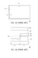
- FIG. 1A is a top view of a conventional thin film solar cell.
- FIG. 1B is a cross-sectional view of the thin film solar cell along the line AA' in FIG. 1A .
- FIG. 1A simply illustrates the top view of films on a first substrate in FIG. 1B but ignores a second substrate and an adhesive between the first substrate and the second substrate.
- the thin film solar cell 100 has an active area P1 and a dead area P2.
- a photovoltaic layer 130 disposed in the active area P1 transforms photonic energy into electric energy.
- a passivation layer 140 such as a white paint, is disposed on the photovoltaic layer 130 and used to protect the photovoltaic layer 130 and electrode layers (not shown) on the sides of the photovoltaic layer 130.
- the electrode layer, the photovoltaic layer 130, the electrode layer, and the passivation layer 140 are disposed on the first substrate 110 in sequence. During the process of stacking these films, they are patterned by using laser scribing processes to manufacturing a plurality of sub-cells in series.
- a process for insulating is proceeded to a peripheral of the first substrate 110, so as to form the dead area P2 shown in FIG. 1A and FIG. 1B . Thereafter, the first substrate 110 and a second substrate 120 are packaged with an adhesive 150, so that the thin film solar cell 100 shown in FIG. 1B is finished.
- the thin film solar cell 100 shown in FIG. 1B there is no passivation layer, such as the above-described white paint, disposed on the peripheral of the photovoltaic layer 130 and the electrode layers on the sides of the photovoltaic layer 130, such as an area 102 shown in FIG. 1B . Accordingly, moisture in air is easy to contact with the photovoltaic layer and the electrode layers by infiltrating into the thin film solar cell 100 through two sides thereof. As a result, leakage current is generated due to the moisture in air, and further an electrical property of the thin film solar cell 100 is affected thereby. It is dangerous for users, and the thin film solar cell's life is reduced.
- a passivation layer such as the above-described white paint
- one embodiment of the present invention provides a thin film solar cell capable of effectively avoiding infiltration of moisture in air and having a good electrical property.
- One embodiment of the present invention provides a fabrication method of a thin film solar cell, by disposing insulating materials on a peripheral of an photovoltaic layer, to effectively avoid infiltration of moisture in air, so as to have the above-described advantage.
- the thin film solar cell includes a first substrate, a first conductive, a photovoltaic layer, a second conductive layer, a first passivation layer, and a second passivation layer.
- the first conductive layer is disposed on the first substrate and located in the active area.
- the photovoltaic layer is disposed on the first conductive layer and located in the active area.
- the second conductive layer is disposed on the photovoltaic layer and located in the active area.
- the first passivation layer is disposed on the second conductive layer and located in the active area.
- the second passivation layer is disposed on a peripheral of the photovoltaic layer and located in the dead area to avoid the photovoltaic layer from contacting with moisture in air.
- a material of the second passivation layer is an insulating material.
- the thin film solar cell further includes a second substrate and an adhesion layer, wherein the adhesion layer covers the first passivation layer and the second passivation layer, and is located between the first substrate and the second substrate to package the first substrate and the second substrate.
- a material of the adhesion layer includes EVA, PVB, Poly Olefin, or PU.
- the photovoltaic layer is a silicon thin film, a III-V compound semiconductor thin film, a II-VI compound semiconductor thin film, or an organic compound semiconductor thin film.
- a material of the silicon thin film includes at least one of a-Si, ⁇ c-Si, a-SiGe, ⁇ c-SiGe, a-SiC, and ⁇ c-SiC, and the silicon thin film is a tandem silicon thin film or a triple silicon thin film.
- a material of the III-V compound semiconductor thin film includes GaAs, InGaP, or a combination thereof.
- a material of the II-VI compound semiconductor thin film includes CIS, CIGS, CdTe, or a combination thereof.
- a material of the organic compound semiconductor thin film includes Poly(3-hexylthiophene) ( P3HT) and a PCBM mixture.
- the first conductive layer is a transparent conductive layer
- the second conductive layer includes one of a reflecting layer and a transparent conductive layer.
- the second conductive layer is a transparent conductive layer
- the first conductive layer includes one of a reflecting layer and a transparent conductive layer.
- One embodiment of the present invention provides a fabrication method of a thin film solar cell.
- the fabrication method includes following steps. First, a first substrate is provided. Next, a first conductive layer is formed on the first substrate. Thereafter, an photovoltaic layer is formed on the first conductive layer. Next, a second conductive layer is formed on the photovoltaic layer. Thereafter, a first passivation layer is formed on the second conductive layer. Next, a portion of the first conductive layer, a portion of the photovoltaic layer, a portion of the second conductive layer, and a portion of the first passivation layer located on a peripheral of the first substrate are removed to define an active region and a dead area on the first substrate. Thereafter, a second passivation layer located in the dead area is formed to cover a peripheral of the photovoltaic layer, so as to avoid the photovoltaic layer contacting moisture in air.
- the fabrication method further includes a step of covering an adhesion layer on the first passivation layer and the second passivation layer to package the first substrate and a second substrate.
- a method of forming the photovoltaic layer includes radio frequency plasma enhanced chemical vapor deposition (RF PECVD), very high frequency plasma enhanced chemical vapor deposition (VHF PECVD, or microwave plasma enhanced chemical vapor deposition (MW PECVD).
- RF PECVD radio frequency plasma enhanced chemical vapor deposition
- VHF PECVD very high frequency plasma enhanced chemical vapor deposition
- MW PECVD microwave plasma enhanced chemical vapor deposition
- a method of forming the first passivation layer and the second passivation layer includes a process of screen printing, dry film lamination, or spin coating.
- a method of defining the active region and the dead area on the first substrate includes a process of etching, sandblasting, edging, or laser scribing.
- the step of forming the first conductive layer further includes a step of forming at least one of a transparent conductive layer and a reflecting layer on the first substrate, wherein the second conductive layer is a transparent conductive layer.
- the step of forming the first conductive layer further includes a step of forming at least one of a transparent conductive layer and a reflecting layer on the first substrate, wherein the first conductive layer is a transparent conductive layer.
- the second passivation layer covers a peripheral of the film structure composed of the first conductive layer, the photovoltaic layer, and the second conductive layer in the thin film solar cell of the embodiment consistent with the present invention. Accordingly, leakage current or bad films due to infiltration of moisture in air are avoided, so that the thin film solar cell has a relatively good electrical property. Moreover, a fabrication method of the thin film solar cell is also provided in the embodiment consistent with the present invention.
- FIG. 1A is a top view of a conventional thin film solar cell.
- FIG. 1B is a cross-sectional view of the thin film solar cell along the line AA' in FIG. 1A .
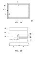
- FIG. 2A is a top view of a thin film solar cell according to an embodiment consistent with the present invention.
- FIG. 2B is a cross-sectional view of the thin film solar cell along the line BB' in FIG. 2A .
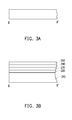
- FIG. 3A through FIG. 3D are schematic cross-sectional views showing steps for manufacturing a thin film solar cell according to an embodiment consistent with the present invention.
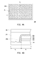
- FIG. 4A is a top view of a thin film solar cell according to another embodiment consistent with the present invention.
- FIG. 4B is a cross-sectional view of the thin film solar cell along the line CC' in FIG. 4A .
- FIG. 5A is a top view of a thin film solar cell according to an embodiment consistent with the present invention.
- FIG. 5B is a cross-sectional view of the thin film solar cell along the line DD' in FIG. 5A .
- FIG. 6A is a top view of a thin film solar cell according to an embodiment consistent with the present invention.
- FIG. 6B is a cross-sectional view of the thin film solar cell along the line EE' in FIG. 6A .
- FIG. 2A is a top view of a thin film solar cell according to an embodiment consistent with the present invention.
- FIG. 2B is a cross-sectional view of the thin film solar cell along the line BB' in FIG. 2A .
- FIG. 2A simply illustrates the top view of films on a first substrate in FIG. 2B but ignores a second substrate and an adhesion layer between the first substrate and the second substrate.
- the thin film solar cell 200 of the present embodiment has an active area P1 and a dead area P2.
- the thin film solar cell 200 includes the first substrate 210, a first conductive 220, an photovoltaic layer 230, a second conductive layer 240, a first passivation layer 250, and a second passivation layer 260.
- the first conductive layer 220 is disposed on the first substrate 210 and located in the active area P2, as shown in FIG. 2B .
- the first substrate 210 may be a transparent substrate, such as a glass substrate.
- the first substrate 210 may be a transparent conductive layer, and a material thereof is at least one of indium tin oxide (ITO), indium zinc oxide (IZO), indium tin zinc oxide (ITZO), zinc oxide, aluminum tin oxide (ATO), aluminum zinc oxide (AZO), cadmium indium oxide (CIO), cadmium zinc oxide (CZO), GZO, and FTO.
- ITO indium tin oxide
- IZO indium zinc oxide
- ITZO indium tin zinc oxide
- ATO aluminum tin oxide
- AZO aluminum zinc oxide
- CIO cadmium indium oxide
- CZO cadmium zinc oxide
- GZO and FTO.
- the first conductive layer 220 may be a reflecting layer (not shown) or a stack of the above-described transparent conductive layer and the reflecting layer, wherein the reflecting layer is located between the transparent conductive layer and the first substrate 210, and a material of the reflecting layer is a metal having high reflectivity, such as silver or aluminum.
- the photovoltaic layer 230 is disposed on the first conductive layer 220 and located in the active area P1 as shown FIG. 2B .
- the photovoltaic layer 230 may be a silicon thin film, a III-V compound semiconductor thin film, a II-VI compound semiconductor thin film, or an organic compound semiconductor thin film.
- a material of the silicon thin film for example, includes at least one of a-Si, ⁇ c-Si, a-SiGe, ⁇ c-SiGe, a-SiC, and ⁇ c-SiC, and the silicon thin film may be a tandem silicon thin film or a triple silicon thin film.
- IIIA material of the III-V compound semiconductor thin film for example, includes GaAs, InGaP, or a combination thereof.
- a material of the II-VI compound semiconductor thin film for example, includes CIS, CIGS, CdTe, or a combination thereof.
- a material of the organic compound semiconductor thin film for example, includes Poly(3-hexylthiophene) ( P3HT) and a PCBM mixture.
- the thin film solar cell 200 may adopt at least one film structure of an amorphous silicon thin film solar cell, a micro-crystalline or nano-crystalline silicon thin film solar cell, a tandem thin film solar cell, a triple thin film solar cell, a copper selenium cadmium (CIS) thin film solar cell, a copper gallium selenium cadmium (CIGS) thin film solar cell, a cadmium tellurium (CdTe) thin film solar cell, and an organic thin film solar cell.
- CIS copper selenium cadmium
- CGS copper gallium selenium cadmium
- CdTe cadmium tellurium
- the photovoltaic layer 230 of the present embodiment may be modified in consideration of the actual demands.
- the above description is merely exemplary.
- the thin film solar cell 200 may adopt another film structure of other thin film solar cells.
- the second conductive layer 240 is disposed on the photovoltaic layer 230 and located in the active area P1 as shown FIG. 2B .
- the second conductive layer 240 may adopt the materials of the above-described transparent conductive layer, and thus, detail descriptions are omitted.
- the second conductive layer 240 may further include the reflecting layer, wherein the reflecting layer is located on the above-described transparent conductive layer. It should be noted that, when the second conductive layer 240 includes the reflecting layer, the first conductive layer 220 is simply the transparent conductive layer. On the contrary, when the first conductive layer 220 includes the reflecting layer, the second conductive layer 240 is simply the transparent conductive layer without the above-described reflecting layer.
- the first conductive layer 220 and the second conductive layer 240 may both the transparent conductive layer without the above-described reflecting layer. In other words, it may be changed for different design requirements, such as a bifacial thin film solar cell or a single-facial thin film solar cell.
- the above description is merely exemplary, and the present invention is not limited herein.
- the first passivation layer 250 is disposed on the second conductive layer 240 and located in the active area P1. In the present embodiment, the first passivation layer 250 is used to avoid the second conductive layer 240 and the films therebelow from contacting with moisture in air which may lower the electrical property of the thin film solar cell 200.
- a material of the first passivation layer 250 is an insulating material. In another embodiment, the material of the first passivation layer 250 may be one of other insulating and transparent materials.
- the second passivation layer 260 is disposed on a peripheral of the photovoltaic layer 240 and located in the dead area P2 to avoid the photovoltaic layer 230 from contacting with moisture in air, as shown in FIG. 2B .
- the second passivation layer 260 since the second passivation layer 260 at least covers the peripheral of the film structure composed of the first conductive 220, the photovoltaic layer 230, and the second conductive layer 240 and contacts with the first passivation layer 250, the first conductive 220, the photovoltaic layer 230, and the second conductive layer 240 are avoided from contacting with moisture in air, as that the thin film solar cell 200 has a better electrical property.
- materials of the first passivation layer 250 and the second passivation layer 260 may be the same transparent materials. That is, the second passivation layer 260 may adopt a suitable material, such as a white paint, for protecting. Similarly, the second passivation layer 260 may be one of other insulating and transparent material.
- the insulating and transparent material may be SiO x , SiN x , SiN x O y , SiC x , hafnium oxide, AlO x , benzocyclobutane (BCB), cycloolefin, polyimide, polyamide, polyester, polyalcohols, polyethylene, polyphenylene, resin, polyether, polyketone, or a combinarion thereof.
- the second passivation layer 260 may adopt a material different from the first passivation layer 250.
- the thin film solar cell 200 further includes a second substrate 280 and an adhesion layer 270, as shown in FIG. 2B .
- the adhesion layer 270 covers the first passivation layer 250 and the second passivation layer 260 and is located between the first substrate 210 and the second substrate 280.
- the adhesion layer 270 is used to package the first substrate 210 and the second substrate 280.
- a material of the adhesion layer 270 may be an adhesive, such as EVA, PVB, Poly Olefin, or PU.
- the thin film solar cell 200 includes the second passivation layer 260 covering the peripheral of the film structure composed of the first conductive 220, the photovoltaic layer 230, and the second conductive layer 240, the first conductive 220, the photovoltaic layer 230, and the second conductive layer 240 are avoided from contacting with moisture in air which causes leakage current or bad films affecting the electrical property of thin film solar cell 200.
- the thin film solar cell 200 including the second passivation layer 260 has a better the electrical property.
- FIG. 3A through FIG. 3D are schematic cross-sectional views showing steps for manufacturing a thin film solar cell according to an embodiment consistent with the present invention.
- FIG. 3A through FIG. 3D simply illustrate the schematic cross-sectional views of the thin film solar cell along the line BB' in FIG. 2A Referring to FIG. 3A , first of all, the first substrate 210 mentioned above is provided.
- the first conductive layer 220 mentioned above is formed on the first substrate 210, as shown in FIG. 3B .
- a method of forming the first conductive layer 220 for example, is sputtering, metal organic chemical vapor deposition (MOCVD), and evaporation.
- MOCVD metal organic chemical vapor deposition
- a first laser scanning process for patterning the first conductive layer 220 is used to form bottom electrodes of sub cells connected in series later. It is well-known to those with ordinary skills in the art and will not be described herein.
- a method of forming the photovoltaic layer 230 includes radio frequency plasma enhanced chemical vapor deposition (RF PECVD), very high frequency plasma enhanced chemical vapor deposition (VHF PECVD, or microwave plasma enhanced chemical vapor deposition (MW PECVD).
- RF PECVD radio frequency plasma enhanced chemical vapor deposition
- VHF PECVD very high frequency plasma enhanced chemical vapor deposition
- MW PECVD microwave plasma enhanced chemical vapor deposition
- the method of forming the photovoltaic layer 230 may be modified according to the film structure adopted by the thin film solar cell, such as the film structure of the above-described silicon thin film solar cell or II-VI compound semiconductor thin film solar cell.
- a second laser scanning process for patterning the photovoltaic layer 230 is used. It is well-known to those with ordinary skills in the art and will not be described herein.
- the second conductive layer 240 mentioned above is formed on the photovoltaic layer 230, as shown in FIG. 3B .
- a method of forming the second conductive layer 240 is similar to the method of forming the first conductive layer 220. It can be referred to the above description and will not be described herein.
- a third laser scanning process for patterning the second conductive layer 240 is used form top electrodes of the sub cells connected in series later. It is well-known to those with ordinary skills in the art and will not be described herein.
- a method of forming the first passivation layer 250 includes a process of screen printing, dry film lamination, or spin coating.
- the process of screen printing is exemplary in detail below.
- a portion of the first conductive layer 220, a portion of the photovoltaic layer 230, a portion of the second conductive layer 240, and a portion of the first passivation layer 250 located on a peripheral of the first substrate 210 are removed to define the above-described active region P1 and the above-described dead area P2 on the first substrate 210, as shown in FIG. 3C .
- a method of removing the above-described films 220, 230, 240, and 250 to define the active region P1 and the dead area P2, for example, is a process of etching, sandblasting, edging, or laser scribing or one of other suitable processes.
- the above-described second passivation layer 260 is formed and located in the dead area P2 to cover a peripheral of the photovoltaic layer 230 to avoid the photovoltaic layer 230 from contacting with moisture in air, as shown in FIG. 3D .
- a method of forming the second passivation layer 260 is similar to the method of forming the first passivation layer 250. It can be referred to the above description and will not be described herein.
- the above-described adhesion layer 270 is covered on the first passivation layer 250 and the second passivation layer 260 to package the above-described first substrate 210 and the above-described second substrate 280. Accordingly, the thin film solar cell 200 shown in FIG. 2B is formed.
- a method of packaging the first substrate 210 and the second substrate 280 by using the adhesion layer 270 is well-known to those with ordinary skilled in the art and will not be described herein. Thereby, the fabrication method of the thin film solar cell is approximately completed.
- FIG. 4A is a top view of a thin film solar cell according to another embodiment consistent with the present invention.
- FIG. 4B is a cross-sectional view of the thin film solar cell along the line CC' in FIG. 4A .
- FIG. 4A simply illustrates the top view of films on a first substrate in FIG. 4B but ignores a second substrate and an adhesion layer between the first substrate and the second substrate.
- the thin film solar cell 300 of the present embodiment is structurally similar to the thin film solar cell 200, and the same reference numbers refer to the same components.
- the difference between the two thin film solar cells 300 and 200 lies in that the second passivation layer 260a is disposed not only on the peripheral of the photovoltaic layer 240 and located in the dead area P2 but also on the first passivation layer 250 to further protect the films below the first passivation layer 250, as shown in FIG. 4A and FIG. 4B .
- the thin film solar cell 300 of the present embodiment also has the same advantages as that of the above-described thin film solar cell 200 do, and it will not be described herein.
- the method of forming the second passivation layer 260a is preferred to spin coating. As a result, not only a process period for forming the second passivation layer 260a but also a manufacturing period for the thin film solar cell 300 is reduced.
- the second passivation layer 260b may overall cover on the active area P1 and the dead area P2, so that the thin film solar cell 400 is formed as shown in FIG. 5A and FIG. 5B.
- FIG. 5A is a top view of a thin film solar cell according to another embodiment consistent with the present invention.
- FIG. 5B is a cross-sectional view of the thin film solar cell along the line DD' in FIG. 5A .
- the thin film solar cell 400 since film structure thereof is similar to that of the thin film solar cell 200 or 300 besides the second passivation layer 260b overall covers on the active area P1 and the dead area P2, the thin film solar cell 400 also has the same advantages as that of the above-described thin film solar cell 200 or 300 do, and it will not be described herein.
- the second passivation layer 260c may cover on a part of the active area P1 and the dead area P2, so that the thin film solar cell 500 is formed as shown in FIG. 6A and FIG. 6B.
- FIG. 6A is a top view of a thin film solar cell according to another embodiment consistent with the present invention.
- FIG. 6B is a cross-sectional view of the thin film solar cell along the line EE' in FIG. 6A .
- the thin film solar cell 500 since film structure thereof is similar to that of the thin film solar cell 200, 300 or 400 besides the second passivation layer 260b covers on a part of the active area P1 and the dead area P2, the thin film solar cell 500 also has the same advantages as that of the above-described thin film solar cell 200, 300, or 400 do, and it will not be described herein.
- the thin film solar cell and the fabrication method thereof is provided in the above-described embodiment. Since the thin film solar cell has the second passivation layer covering on the peripheral of the film structure composed of the first conductive layer, the photovoltaic layer, and the second conductive layer, leakage current or bad films, which may lower the electrical property of the thin film solar cell, due to infiltration of moisture in air are avoided. In other words, the thin film solar cell of the embodiment consistent with the present invention has a better electrical property. Moreover, the fabrication method of the thin film solar cell is also provided in the embodiment consistent with the present invention.
Landscapes
- Photovoltaic Devices (AREA)
Applications Claiming Priority (1)
| Application Number | Priority Date | Filing Date | Title |
|---|---|---|---|
| TW098115711A TW201041158A (en) | 2009-05-12 | 2009-05-12 | Thin film solar cell and manufacturing method thereof |
Publications (1)
| Publication Number | Publication Date |
|---|---|
| EP2251908A2 true EP2251908A2 (fr) | 2010-11-17 |
Family
ID=41727538
Family Applications (1)
| Application Number | Title | Priority Date | Filing Date |
|---|---|---|---|
| EP10150014A Withdrawn EP2251908A2 (fr) | 2009-05-12 | 2010-01-04 | Cellule solaire à film mince et son procédé de fabrication |
Country Status (4)
| Country | Link |
|---|---|
| US (2) | US20100288349A1 (fr) |
| EP (1) | EP2251908A2 (fr) |
| DE (1) | DE10150014T1 (fr) |
| TW (1) | TW201041158A (fr) |
Families Citing this family (2)
| Publication number | Priority date | Publication date | Assignee | Title |
|---|---|---|---|---|
| US8697478B2 (en) * | 2012-09-06 | 2014-04-15 | Tsmc Solar Ltd. | Cover for protecting solar cells during fabrication |
| WO2018193747A1 (fr) * | 2017-04-19 | 2018-10-25 | Sony Semiconductor Solutions Corporation | Dispositif à semi-conducteur, son procédé de fabrication et appareil électronique |
Family Cites Families (21)
| Publication number | Priority date | Publication date | Assignee | Title |
|---|---|---|---|---|
| US4331492A (en) * | 1979-10-17 | 1982-05-25 | Solarex Corporation | Method of making a solar panel |
| US5176758A (en) * | 1991-05-20 | 1993-01-05 | United Solar Systems Corporation | Translucent photovoltaic sheet material and panels |
| US5356488A (en) * | 1991-12-27 | 1994-10-18 | Rudolf Hezel | Solar cell and method for its manufacture |
| JP3651932B2 (ja) * | 1994-08-24 | 2005-05-25 | キヤノン株式会社 | 光起電力素子用裏面反射層及びその形成方法並びに光起電力素子及びその製造方法 |
| US7732243B2 (en) * | 1995-05-15 | 2010-06-08 | Daniel Luch | Substrate structures for integrated series connected photovoltaic arrays and process of manufacture of such arrays |
| WO2002075816A1 (fr) * | 2001-03-19 | 2002-09-26 | Shin-Etsu Handotai Co.,Ltd. | Pile solaire et son procede de fabrication |
| JP2003031824A (ja) * | 2001-07-13 | 2003-01-31 | Sharp Corp | 太陽電池モジュール |
| JP3841790B2 (ja) * | 2002-03-06 | 2006-11-01 | シャープ株式会社 | 光電変換素子及びその製造方法 |
| FR2883663B1 (fr) * | 2005-03-22 | 2007-05-11 | Commissariat Energie Atomique | Procede de fabrication d'une cellule photovoltaique a base de silicium en couche mince. |
| JP5010468B2 (ja) * | 2005-03-24 | 2012-08-29 | 京セラ株式会社 | 光電変換素子とその製造方法、及びこれを用いた光電変換モジュール |
| US20100147379A1 (en) * | 2005-10-03 | 2010-06-17 | Katsushi Kishimoto | Silicon-based thin-film photoelectric conversion device, and method and apparatus for manufacturing the same |
| US20080023067A1 (en) * | 2005-12-27 | 2008-01-31 | Liangbing Hu | Solar cell with nanostructure electrode |
| TW200814393A (en) * | 2006-07-18 | 2008-03-16 | Univ Southern California | Organic optoelectronic device electrodes with nanotubes |
| US20090038669A1 (en) * | 2006-09-20 | 2009-02-12 | Translucent Photonics, Inc. | Thin Film Solar Cell III |
| US20080121264A1 (en) * | 2006-11-28 | 2008-05-29 | Industrial Technology Research Institute | Thin film solar module and method of fabricating the same |
| US7982126B2 (en) * | 2007-05-21 | 2011-07-19 | Macfarlane Alexander T | Photovoltaic module with improved heat transfer and recovery potential |
| US8247254B2 (en) * | 2007-07-13 | 2012-08-21 | Silicon China (HK) Ltd. | System and method for forming solar cell structures |
| ATE498203T1 (de) * | 2007-07-23 | 2011-02-15 | Basf Se | Photovoltaische tandem-zelle |
| US20090158750A1 (en) * | 2007-12-14 | 2009-06-25 | Matthew Rubin | Novel solid state thermovoltaic device for isothermal power generation and cooling |
| US20090229664A1 (en) * | 2008-03-17 | 2009-09-17 | Nanopv Technologies Inc. | Method of manufacturing nanocrystalline photovoltaic devices |
| US8916769B2 (en) * | 2008-10-01 | 2014-12-23 | International Business Machines Corporation | Tandem nanofilm interconnected semiconductor wafer solar cells |
-
2009
- 2009-05-12 TW TW098115711A patent/TW201041158A/zh unknown
- 2009-12-04 US US12/630,844 patent/US20100288349A1/en not_active Abandoned
-
2010
- 2010-01-04 EP EP10150014A patent/EP2251908A2/fr not_active Withdrawn
- 2010-01-04 DE DE10150014T patent/DE10150014T1/de active Pending
-
2011
- 2011-06-08 US US13/155,975 patent/US20110237017A1/en not_active Abandoned
Non-Patent Citations (1)
| Title |
|---|
| None |
Also Published As
| Publication number | Publication date |
|---|---|
| TW201041158A (en) | 2010-11-16 |
| DE10150014T1 (de) | 2011-05-05 |
| US20100288349A1 (en) | 2010-11-18 |
| US20110237017A1 (en) | 2011-09-29 |
Similar Documents
| Publication | Publication Date | Title |
|---|---|---|
| US9246131B2 (en) | Layered element for encapsulating a senstive element | |
| US12211656B2 (en) | Photovoltaic structure and method of fabrication | |
| US8212143B2 (en) | Thin film solar cell and manufacturing method thereof | |
| US20120145233A1 (en) | Back contact solar cell and manufacturing method thereof | |
| KR20210124521A (ko) | 박막 광기전 모듈 상호연결부들 내에서의 바이패스 다이오드들의 통합 | |
| JP6055787B2 (ja) | 太陽電池及びその製造方法 | |
| GB2339963A (en) | Photovoltaic module | |
| US20120000506A1 (en) | Photovoltaic module and method of manufacturing the same | |
| US11810984B1 (en) | Photovoltaic cell, method for preparing same, and photovoltaic module | |
| US20110088764A1 (en) | Solar cell and manufacturing method thereof | |
| CN110574170A (zh) | 一种柔性薄膜太阳电池及其制造方法 | |
| US20130105930A1 (en) | Method for making semiconductor light detection devices | |
| JP3755048B2 (ja) | 集積化薄膜タンデム太陽電池とその製造方法 | |
| EP2341547A2 (fr) | Cellule solaire à film mince et son procédé de fabrication | |
| EP2251908A2 (fr) | Cellule solaire à film mince et son procédé de fabrication | |
| US20110120534A1 (en) | Thin film solar cell and manufacturing method thereof | |
| US20110088779A1 (en) | Method for manufacturing thin-film solar cell and thin-film solar cell | |
| KR101081095B1 (ko) | 태양전지 및 이의 제조방법 | |
| CN120981098B (zh) | 叠层太阳能电池及光伏组件 | |
| CN102255004A (zh) | 一种薄膜太阳能电池的制造方法 | |
| KR102396820B1 (ko) | 태양 전지 모듈 및 그 제조 방법 | |
| JP4173692B2 (ja) | 太陽電池素子およびその製造方法 | |
| TW201324829A (zh) | 薄膜太陽能電池的製作方法 | |
| KR101072067B1 (ko) | 팁, 태양전지 및 이를 이용한 태양전지 제조방법 | |
| TW201123476A (en) | Thin film solar cell and fabrication method thereof |
Legal Events
| Date | Code | Title | Description |
|---|---|---|---|
| PUAI | Public reference made under article 153(3) epc to a published international application that has entered the european phase |
Free format text: ORIGINAL CODE: 0009012 |
|
| AK | Designated contracting states |
Kind code of ref document: A2 Designated state(s): AT BE BG CH CY CZ DE DK EE ES FI FR GB GR HR HU IE IS IT LI LT LU LV MC MK MT NL NO PL PT RO SE SI SK SM TR |
|
| AX | Request for extension of the european patent |
Extension state: AL BA RS |
|
| DET | De: translation of patent claims | ||
| REG | Reference to a national code |
Ref country code: DE Ref legal event code: R210 Effective date: 20110505 |
|
| STAA | Information on the status of an ep patent application or granted ep patent |
Free format text: STATUS: THE APPLICATION IS DEEMED TO BE WITHDRAWN |
|
| 18D | Application deemed to be withdrawn |
Effective date: 20130801 |