EP2249631A1 - Multilayer circuit board, and motor-driving circuit board - Google Patents
Multilayer circuit board, and motor-driving circuit board Download PDFInfo
- Publication number
- EP2249631A1 EP2249631A1 EP09708156A EP09708156A EP2249631A1 EP 2249631 A1 EP2249631 A1 EP 2249631A1 EP 09708156 A EP09708156 A EP 09708156A EP 09708156 A EP09708156 A EP 09708156A EP 2249631 A1 EP2249631 A1 EP 2249631A1
- Authority
- EP
- European Patent Office
- Prior art keywords
- wiring
- circuit board
- multilayer circuit
- wirings
- conductor layers
- Prior art date
- Legal status (The legal status is an assumption and is not a legal conclusion. Google has not performed a legal analysis and makes no representation as to the accuracy of the status listed.)
- Granted
Links
Images



Classifications
-
- H—ELECTRICITY
- H05—ELECTRIC TECHNIQUES NOT OTHERWISE PROVIDED FOR
- H05K—PRINTED CIRCUITS; CASINGS OR CONSTRUCTIONAL DETAILS OF ELECTRIC APPARATUS; MANUFACTURE OF ASSEMBLAGES OF ELECTRICAL COMPONENTS
- H05K1/00—Printed circuits
- H05K1/02—Details
- H05K1/0213—Electrical arrangements not otherwise provided for
- H05K1/0216—Reduction of cross-talk, noise or electromagnetic interference
- H05K1/0228—Compensation of cross-talk by a mutually correlated lay-out of printed circuit traces, e.g. for compensation of cross-talk in mounted connectors
-
- B—PERFORMING OPERATIONS; TRANSPORTING
- B62—LAND VEHICLES FOR TRAVELLING OTHERWISE THAN ON RAILS
- B62D—MOTOR VEHICLES; TRAILERS
- B62D5/00—Power-assisted or power-driven steering
- B62D5/04—Power-assisted or power-driven steering electrical, e.g. using an electric servo-motor connected to, or forming part of, the steering gear
- B62D5/0403—Power-assisted or power-driven steering electrical, e.g. using an electric servo-motor connected to, or forming part of, the steering gear characterised by constructional features, e.g. common housing for motor and gear box
- B62D5/0406—Power-assisted or power-driven steering electrical, e.g. using an electric servo-motor connected to, or forming part of, the steering gear characterised by constructional features, e.g. common housing for motor and gear box including housing for electronic control unit
-
- H—ELECTRICITY
- H02—GENERATION; CONVERSION OR DISTRIBUTION OF ELECTRIC POWER
- H02M—APPARATUS FOR CONVERSION BETWEEN AC AND AC, BETWEEN AC AND DC, OR BETWEEN DC AND DC, AND FOR USE WITH MAINS OR SIMILAR POWER SUPPLY SYSTEMS; CONVERSION OF DC OR AC INPUT POWER INTO SURGE OUTPUT POWER; CONTROL OR REGULATION THEREOF
- H02M7/00—Conversion of AC power input into DC power output; Conversion of DC power input into AC power output
- H02M7/003—Constructional details, e.g. physical layout, assembly, wiring or busbar connections
-
- H—ELECTRICITY
- H02—GENERATION; CONVERSION OR DISTRIBUTION OF ELECTRIC POWER
- H02M—APPARATUS FOR CONVERSION BETWEEN AC AND AC, BETWEEN AC AND DC, OR BETWEEN DC AND DC, AND FOR USE WITH MAINS OR SIMILAR POWER SUPPLY SYSTEMS; CONVERSION OF DC OR AC INPUT POWER INTO SURGE OUTPUT POWER; CONTROL OR REGULATION THEREOF
- H02M1/00—Details of apparatus for conversion
- H02M1/44—Circuits or arrangements for compensating for electromagnetic interference in converters or inverters
-
- H—ELECTRICITY
- H05—ELECTRIC TECHNIQUES NOT OTHERWISE PROVIDED FOR
- H05K—PRINTED CIRCUITS; CASINGS OR CONSTRUCTIONAL DETAILS OF ELECTRIC APPARATUS; MANUFACTURE OF ASSEMBLAGES OF ELECTRICAL COMPONENTS
- H05K1/00—Printed circuits
- H05K1/02—Details
- H05K1/0213—Electrical arrangements not otherwise provided for
- H05K1/0263—High current adaptations, e.g. printed high current conductors or using auxiliary non-printed means; Fine and coarse circuit patterns on one circuit board
-
- H—ELECTRICITY
- H05—ELECTRIC TECHNIQUES NOT OTHERWISE PROVIDED FOR
- H05K—PRINTED CIRCUITS; CASINGS OR CONSTRUCTIONAL DETAILS OF ELECTRIC APPARATUS; MANUFACTURE OF ASSEMBLAGES OF ELECTRICAL COMPONENTS
- H05K1/00—Printed circuits
- H05K1/02—Details
- H05K1/0296—Conductive pattern lay-out details not covered by sub groups H05K1/02 - H05K1/0295
- H05K1/0298—Multilayer circuits
-
- H—ELECTRICITY
- H05—ELECTRIC TECHNIQUES NOT OTHERWISE PROVIDED FOR
- H05K—PRINTED CIRCUITS; CASINGS OR CONSTRUCTIONAL DETAILS OF ELECTRIC APPARATUS; MANUFACTURE OF ASSEMBLAGES OF ELECTRICAL COMPONENTS
- H05K2201/00—Indexing scheme relating to printed circuits covered by H05K1/00
- H05K2201/09—Shape and layout
- H05K2201/09209—Shape and layout details of conductors
- H05K2201/09654—Shape and layout details of conductors covering at least two types of conductors provided for in H05K2201/09218 - H05K2201/095
- H05K2201/09672—Superposed layout, i.e. in different planes
-
- H—ELECTRICITY
- H05—ELECTRIC TECHNIQUES NOT OTHERWISE PROVIDED FOR
- H05K—PRINTED CIRCUITS; CASINGS OR CONSTRUCTIONAL DETAILS OF ELECTRIC APPARATUS; MANUFACTURE OF ASSEMBLAGES OF ELECTRICAL COMPONENTS
- H05K2201/00—Indexing scheme relating to printed circuits covered by H05K1/00
- H05K2201/10—Details of components or other objects attached to or integrated in a printed circuit board
- H05K2201/10007—Types of components
- H05K2201/10166—Transistor
-
- H—ELECTRICITY
- H10—SEMICONDUCTOR DEVICES; ELECTRIC SOLID-STATE DEVICES NOT OTHERWISE PROVIDED FOR
- H10W—GENERIC PACKAGES, INTERCONNECTIONS, CONNECTORS OR OTHER CONSTRUCTIONAL DETAILS OF DEVICES COVERED BY CLASS H10
- H10W72/00—Interconnections or connectors in packages
- H10W72/50—Bond wires
- H10W72/541—Dispositions of bond wires
- H10W72/5445—Dispositions of bond wires being orthogonal to a side surface of the chip, e.g. parallel arrangements
-
- H—ELECTRICITY
- H10—SEMICONDUCTOR DEVICES; ELECTRIC SOLID-STATE DEVICES NOT OTHERWISE PROVIDED FOR
- H10W—GENERIC PACKAGES, INTERCONNECTIONS, CONNECTORS OR OTHER CONSTRUCTIONAL DETAILS OF DEVICES COVERED BY CLASS H10
- H10W72/00—Interconnections or connectors in packages
- H10W72/50—Bond wires
- H10W72/541—Dispositions of bond wires
- H10W72/547—Dispositions of multiple bond wires
- H10W72/5475—Dispositions of multiple bond wires multiple bond wires connected to common bond pads at both ends of the wires
Definitions
- a motor drive circuit board for an electric power steering system comprising: a multilayer circuit board which includes a plurality of conductor layers and a plurality of resin insulation layers which are laminated alternately; a first wiring formed on a first layer of the plurality of conductor layers; and a second wiring formed on a second layer of the plurality of conductor layers, wherein portions of the first wiring and the second wiring which face each other in a direction in which the plurality of conductor layers are laminated extend in parallel; and wherein the first wiring and the second wiring are arranged so as to weaken a magnetic field generated by a current which flows through the first wiring and a magnetic field generated by a current which flows through the second wiring to each other.
- Fig. 1 is an external plan view of a multilayer circuit board according to one embodiment of the invention
- Fig. 2 is an external plan view of the multilayer circuit board with those other than components and wirings which are included in the circuit board made transparent
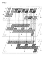
- Fig. 3 is an exploded perspective view showing respective constructions of layers of the multilayer circuit board.
- Fig. 4 is a circuit diagram of the motor drive circuit.
- drain terminals of the MOSFETs 15u, 15v, 15w which are included in the motor drive circuit are connected to positive poles of the power source, not shown, and source terminals thereof are connected to the corresponding phase input terminals of the motor, respectively.
- Source terminals of the MOSFETs 16u, 16v, 16w which are included in the motor drive circuit are connected to the negative pole (the ground pole) of the power source, not shown, via the resistor 17, and drain terminals thereof are connected to the corresponding phase input terminals of the motor, respectively.
- a connecting relationship of the motor drive circuit shown in Fig. 4 corresponds to a connecting relationship between the respective layers shown in Fig. 3 .
- dotted lines extending in a vertical direction in Fig. 3 denote positions of through holes. Since conductor layers (typically, copper plated layers) are formed on inner faces of the through holes, energization or electrical communication is established between the conductors linked to both ends of the through holes. Consequently, as is shown in the circuit diagram in Fig.
- the ground wiring 22 and the power source wiring 33 are disposed so that most of the wirings are superposed vertically.
- the inductance of these wirings is reduced. Namely, since the ground wiring 22 is connected to the ground terminal 20 in the vicinity of a rightward lower end portion in the figure (via the through hole and the resistor 17), a current flows therethrough from the right towards the left of the figure. Consequently, the currents flow in an opposite direction to each other along the direction of the longer side in the portions of the ground wiring 22 and the power source wiring 33 which are superposed. Therefore, since magnetic fields generated by these currents are canceled by each other (namely, since a mutual inductance becomes large), the inductance of these wirings which generally extend long from the terminals can be reduced.
- a multilayer circuit board such as the multilayer circuit boards 100, 110 described above may be used.
- This heat dissipating land 312 is brought into press contact with a projecting portion 302 which is formed underneath an upper gear housing 301 via a heat conduction sheet 321.
- heat of the CPU 330 is transferred to the upper gear housing 301 having a large heat capacity.
- the heat of the CPU 330 is dissipated with good efficiency.
- a configuration may be adopted in which in place of the heat conduction sheet 321, a gel containing a material having heat conduction properties may be applied.
- the CPU 330 has been described as representing an element having a large heat capacity, and this heat dissipating configuration may be applied to other electronic components.
- the configuration in question may be adopted for the MOSFETs 15u, 15v, 15w, 16u, 16v, 16w which are provided on the multilayer circuit boards 100, 110 described above.
- Fig. 9 is a schematic sectional view showing configurations of a bare chip and a non-contacting heat sink.
- a bare chip 450 is mounted on an electronic circuit board 403, and a normal heat sink 404 is attached to a rear face (a lower face in the figure) of the electronic circuit board 403.
- a coating resin 402 is applied to the periphery of the bare chip 405, and a non-contacting heat sink 401 is disposed directly above the bare chip 405 in a closest position so as to face the bare chip 405.
- This non-contacting heat sink 401 is fixed to a housing having a larger heat capacity.
- the invention can provide the multilayer circuit board in which the wirings are arranged so that the inductance thereof is reduced and a motor drive circuit board employing the multilayer circuit board which is used in an electric power steering system.
Landscapes
- Engineering & Computer Science (AREA)
- Physics & Mathematics (AREA)
- Electromagnetism (AREA)
- Microelectronics & Electronic Packaging (AREA)
- Chemical & Material Sciences (AREA)
- Combustion & Propulsion (AREA)
- Transportation (AREA)
- Mechanical Engineering (AREA)
- Power Engineering (AREA)
- Power Steering Mechanism (AREA)
- Structure Of Printed Boards (AREA)
Abstract
Description
- The present invention relates to a multilayer circuit board and a motor drive circuit board for an electric power steering system which employs the multilayer circuit board.
- In an electric power steering system for a vehicle, a steering assist motor is driven so as to obtain a preferred steering assist force in accordance with a steering torque given to a steering wheel by a driver and a vehicle speed.
The steering assist motor is driven by a motor drive circuit which is incorporated in an electronic control unit (hereinafter, referred to as ECU). The motor drive circuit controls large power of the order of 500W to 2000W when it drives the steering assist motor. - As this occurs, the motor drive circuit generates heat, in order to prevent erroneous operations or failure of the ECU due to the generated heat, the motor drive circuit is mounted on a circuit board having good heat conduction properties. As is shown in
Fig. 10(a) , for example, the motor drive circuit is mounted on a metallic circuit board in which oneconductor layer 91 made of copper and oneinsulation layer 92 made of resin are formed one on top of the other on a metallic substrate 93 (a heat sink) made of aluminum. - Since electronic components can only be mounted on one side (specifically, on the conductor layer 91) of the circuit board shown in
Fig. 10(a) , an area occupied by this circuit board within the ECU becomes large. Then, as one of methods for reducing the substrate area, a method is considered in which a circuit board is fabricated with a multiplicity of layers, as is shown inFig. 10(b) . A ceramic multilayer substrate shown inFig. 10(b) is such thatcopper conductor layers 91 andceramic insulation layers 94 are laminated into a multilayer construction, which is then affixed to an aluminum metallic substrate 93 (a heat sink) with an adhesive 95. By adopting the multilayer construction, since the length of circuit conductors (the length of wirings) can be shortened, the inductance thereof can be suppressed to a lower level, thereby making it possible to suppress the generation of switching noise. - In relation to the invention of this patent application, the following related-art techniques are known.
Patent Document 1 discloses an electric power steering system which includes a circuit case which is assembled to a heat sink while covering a power substrate including a switching element and in which the heat sink is assembled to a speed reduction mechanism.Patent Document 2 discloses an electric power steering system in which a power circuit board and a control circuit board are installed to be laminated one on top of the other in a circuit casing and the power circuit board is assembled closely to a bracket of a motor. These constructions eliminate wiring harnesses and connectors so as to reduce radiation noise. Further,Patent Document 3 discloses a configuration in which a substrate including a motor drive circuit and a control circuit is mounted on a motor case to thereby stabilize the operations of the circuits. - Patent Document 1:
JP-A-2002-120739 - Patent Document 2:
JP-A-2002-345211 - Patent Document 3:
WO99/16654 - As has been described above, although in the event that the length of circuit conductors (the length of wirings) is shortened by fabricating a substrate into a multilayer construction, the generation of switching noise can be suppressed, there may be a case in which the length of wirings becomes long depending upon a place where such a multilayer circuit board is mounted. For example, when a place where a circuit board is mounted is narrow and long, the length of a longer side of a substrate becomes much longer than the length of a shorter side thereof. As this occurs, since the inductance of a wiring which extends in the direction of the longer side increases, switching noise increases accordingly.
- Then, an object of the invention is to provide a multilayer circuit board in which wirings are arranged so that the inductance is decrease, and a motor drive circuit board for an electric power steering system which employs the multilayer circuit board.
- According to a first invention, there is provided a multilayer circuit board including a plurality of conductor layers and a plurality of resin insulation layers which are laminated alternately, comprising: a first wiring formed on a first layer of the plurality of conductor layers; and a second wiring formed on a second layer of the plurality of conductor layers, wherein portions of the first wiring and the second wiring which face each other in a direction in which the plurality of conductor layers are laminated extend in parallel; and wherein the first wiring and the second wiring are arranged so as to weaken a magnetic field generated by a current which flows through the first wiring and a magnetic field generated by a current which flows through the second wiring to each other.
- According to a second invention, there is provided a multilayer circuit board according to the first invention, the first wiring and the second wiring are a power source wiring and a ground wiring in which currents flow therethrough in an opposite direction to each other.
- According to a third invention, there is provided a multilayer circuit board according to the first invention, further including a third wiring formed on a third layer of the plurality of conductor layers, wherein the first wiring, the second wiring and the third wiring are wirings which are respectively connected to phases of a multiphase motor provided outside.
- According to a fourth invention, there is provided a multilayer circuit board according to any of the first to third inventions, further including a terminal which is provided in a vicinity of at least one of two short edges of four edges of a substrate surface which is configured by curved lines or straight lines, and is connected to at least one of the first wiring and the second wiring, wherein the portions of the first wiring and the second wiring which face each other extend along two long edges of the four edges.
- According to a fifth invention, there is provided a motor drive circuit board for an electric power steering system comprising: a multilayer circuit board which includes a plurality of conductor layers and a plurality of resin insulation layers which are laminated alternately; a first wiring formed on a first layer of the plurality of conductor layers; and a second wiring formed on a second layer of the plurality of conductor layers, wherein portions of the first wiring and the second wiring which face each other in a direction in which the plurality of conductor layers are laminated extend in parallel; and wherein the first wiring and the second wiring are arranged so as to weaken a magnetic field generated by a current which flows through the first wiring and a magnetic field generated by a current which flows through the second wiring to each other.
- According to the first invention, since the wirings are arranged so that the magnetic fields are canceled by each other, the inductance of the wirings can be made small. In addition, the switching noise that is generated thereby can be suppressed to a lower level. Further, since the inductance of the wirings is small, the substrate can be lengthened in the direction in which the wirings extend.
- According to the second invention, the inductance of the power line and the ground line which generally extend long from the terminals can be made small.
- According to the third invention, the inductance of at least the three wirings which generally extend long from the terminals to connect, respectively, to the phases of the multiphase motor can be made small.
- According to the fourth invention, since the terminals are provided in the vicinity of at least one of the two shorter edges (typically, the shorter sides) of the main four edges (typically, the four sides) of the substrate surface, even in the event that a place where to accommodate the circuit board is narrow and long to extend along the two longer edges (typically, the longer sides) of the edges, the circuit board can easily be placed (accommodated) in the place in question without being interrupted by the wirings extending individually from the terminals.
- According to the fifth invention, the advantage provided in the first invention can also be provided in the motor drive circuit board.
-
- [
Fig. 1 ] An external plan view of a multilayer circuit board according to one embodiment of the invention. - [
Fig. 2 ] An external plan view of the multilayer circuit board with those other than components and wirings which are included in the circuit board made transparent in the embodiment. - [
Fig. 3 ] An exploded perspective view showing respective constructions of layers of the multilayer circuit board according to the embodiment. - [
Fig. 4 ] A circuit diagram of a motor drive circuit of the embodiment. - [
Fig. 5 ] An external plan view of a multilayer circuit board having another different configuration from the multilayer circuit board of the embodiment. - [
Fig. 6 ] An external plan view of the multilayer circuit board having the other configuration with those other than components and wirings which are included in the circuit board made transparent in the embodiment shown inFig. 5 . - [
Fig. 7 ] A sectional view showing a metallic substrate and a heat sink which are screwed together so as to eliminate a clearance on a substrate surface in the embodiment. - [
Fig. 8 ] An exploded perspective view showing schematically a construction for allowing heat of CPU to escape to a gear housing in the embodiment. - [
Fig. 9 ] A schematic sectional view showing constructions of a bare chip and a non-contacting heat sink in the embodiment. - [
Fig. 10 ] A sectional view of a conventional circuit board. - 10u U-phase terminal; 10v V-phase terminal; 10w W-phase terminal; 11 W-phase wiring; 15u, 15v, 15w, 16u, 16v, 16w MOSFET; 17 resistor; 20 ground terminal; 21 V-phase wiring; 22 ground wiring; 30 power source terminal; 31 U-phase terminal; 33 power source wiring; 100 multilayer circuit board; 101 first layer; 102 second layer; 103 third layer; 201 circuit conductor; 202 insulation layer; 203 metallic substrate; 204 heat sink; 205a, 205b screw; 301 upper gear housing; 310 control circuit board; 311 heat dissipating through hole; 321 heat conduction sheet; 330 CPU; 401 non-contacting heat sink; 402 coating resin; 403 electronic circuit board; 404 heat sink; 405 bare chip.
- A multilayer circuit board according to an embodiment of the invention is a motor drive circuit board for an electric power steering system, and this motor drive circuit board is incorporated for use in an ECU (Electronic Control Unit) for the electric power steering system.
- This ECU includes a motor control circuit for calculating a quantity of drive current that is supplied to the steering assist motor and a motor drive circuit for controlling a large current to drive the steering assist motor. Although the heat value of the motor control circuit is small and the current which flows therethrough is small when the circuit operates, the heat value of the motor drive circuit is large and the current which flows therethrough is large when the circuit operates. The motor drive circuit is mounted on a motor drive circuit board, and the motor control circuit is mounted on a separate circuit board from the motor drive circuit board. These two circuit boards are disposed side by side or superposed one on top of the other into two stages in an interior of the ECU. Hereinafter, the construction of the multilayer circuit board, which is the motor drive circuit board, will be described by reference to
Figs. 1 to 3 . -
Fig. 1 is an external plan view of a multilayer circuit board according to one embodiment of the invention,Fig. 2 is an external plan view of the multilayer circuit board with those other than components and wirings which are included in the circuit board made transparent, andFig. 3 is an exploded perspective view showing respective constructions of layers of the multilayer circuit board. - A
multilayer circuit board 100 shown in these figures has a three-layer construction in which a first layer (a top layer) 101, asecond layer 102 and athird layer 103, which are all conductor layers and insulation layers which are provided between those conductor layers are bonded together through thermocompression bonding. The conductor layers are made of metal such as copper having high conduction properties, and the insulation layers are made of a composite material (a so-called, prepreg) in which a glass fiber is impregnated with an insulation resin material. Screw holes are opened in a top right-hand corner and a bottom left-hand corner of themultilayer circuit board 100 as viewed in the figure so that the circuit board is screwed to an aluminum base or a heat sink. - A
resistor 17 and sixMOSFETs multilayer circuit board 100. Connecting terminals at upper portions of these MOSFETs are connected individually to wiring conductors which are provided in predetermined positions on thefirst layer 101 with four aluminum wires through wire bonding. Further, a U-phase terminal 10u which is connected to a U-phase input terminal, a V-phase terminal 10v which is connected to a V-phase input terminal and a W-phase terminal 10w which is connected to a W-phase input terminal of a steering assist motor, not shown, are provided on thefirst layer 101 of themultilayer circuit board 100. Furthermore, a W-phase wiring 11 which is linked to the W-phase terminal 10w, aground terminal 20 which is linked to theresistor 17 and which is connected to a negative pole (a ground pole) provided in a power source unit, not shown, which lies outside the circuit board and apower source terminal 30 are provided on thefirst layer 101. - In addition to the
MOSFETs resistor 17, electronic components that are to be mounted on themultilayer circuit board 100 which is the motor drive circuit board may include a current detection sensor, a noise removing coil, a power source interrupting relay, a motor phase current interrupting relay and the like. - Next, a
ground wiring 22 which is linked to theground terminal 20 on thefirst layer 101 and a V-phase wiring 21 which is linked to the V-phase terminal 10v on thefirst layer 101 are provided on thesecond layer 102 of themultilayer circuit board 100. In addition, a power source wiring 33 which is connected to thepower source terminal 30 on thefirst layer 101 and aU-phase wiring 31 which is linked to theU-phase terminal 10u are provided on thethird layer 103 of themultilayer circuit board 100. - Here, the configuration of the motor drive circuit will be described by reference to
Fig. 4. Fig. 4 is a circuit diagram of the motor drive circuit. As is shown inFig. 4 , drain terminals of the MOSFETs 15u, 15v, 15w which are included in the motor drive circuit are connected to positive poles of the power source, not shown, and source terminals thereof are connected to the corresponding phase input terminals of the motor, respectively. Source terminals of the MOSFETs 16u, 16v, 16w which are included in the motor drive circuit are connected to the negative pole (the ground pole) of the power source, not shown, via theresistor 17, and drain terminals thereof are connected to the corresponding phase input terminals of the motor, respectively. - Referring to
Fig. 3 in association withFig. 4 , it is seen that a connecting relationship of the motor drive circuit shown inFig. 4 corresponds to a connecting relationship between the respective layers shown inFig. 3 . Namely, dotted lines extending in a vertical direction inFig. 3 denote positions of through holes. Since conductor layers (typically, copper plated layers) are formed on inner faces of the through holes, energization or electrical communication is established between the conductors linked to both ends of the through holes. Consequently, as is shown in the circuit diagram inFig. 4 , theresistor 17 and the sixMOSFETs phase wiring 11, V-phase wiring 21,U-phase wiring 31, theground wiring 22, and the power source wiring 33 which are shown inFig. 3 . - As is seen from
Figs. 2 and3 , in the wirings described above, theground wiring 22 and thepower source wiring 33 are disposed so that most of the wirings are superposed vertically. By this configuration, the inductance of these wirings is reduced. Namely, since theground wiring 22 is connected to theground terminal 20 in the vicinity of a rightward lower end portion in the figure (via the through hole and the resistor 17), a current flows therethrough from the right towards the left of the figure.
Consequently, the currents flow in an opposite direction to each other along the direction of the longer side in the portions of theground wiring 22 and the power source wiring 33 which are superposed. Therefore, since magnetic fields generated by these currents are canceled by each other (namely, since a mutual inductance becomes large), the inductance of these wirings which generally extend long from the terminals can be reduced. - Similarly, in the wirings described above, the W-
phase wiring 11, the V-phase wiring 21 andU-phase wiring 31 are also disposed so as to be superposed partially along the longer side direction of themultilayer circuit board 100. By this configuration, the inductance of these wirings is also reduced. Namely, when a general motor control is implemented, a sum of U-phase current, V-phase current and W-phase current becomes zero at all times. By this, magnetic fields generated by currents which flow along the longer side direction in the superposed portions of the W-phase wiring 11, V-phase wiring 21 and W-phase wiring 31 which are canceled by each other (the inductance becomes large). Consequently, the inductance of these wirings which tend to extend long from the terminals can be reduced in a similar fashion. - In this way, since even in the event that the length of the
multilayer circuit board 100 is lengthened in the longer side direction, the inductance of the wirings can be suppressed, the length of themultilayer circuit board 100 in the longer side direction thereof can be made longer than the length in the shorter side direction to a significant extent, and the length of themultilayer circuit board 100 in the shorter side direction can be made smaller without changing the area thereof. Consequently, even in the event that a place where to install themultilayer circuit board 100 is narrow and long, themultilayer circuit board 100 can easily be installed (accommodated) therein. - When the
multilayer circuit board 100 is installed (accommodated) in the narrow and long place, however, there is a case in which the position of theground terminal 20 provided on the longer side of themultilayer circuit board 100 becomes a problem. This is because in certain circumstances, the wiring (the wire) cannot be laid to extend from theground terminal 20 towards the shorter side direction of themultilayer circuit board 100 due to an obstacle lying along the longer side thereof. As this occurs, as is shown inFigs. 5 and 6 , aground terminal 20 is preferably provided on a shorter side of amultilayer circuit board 110. -
Fig. 5 is an external plan view of a multilayer circuit board which has another different configuration from the multilayer circuit board according to the embodiment.Fig. 6 is an external plan view of the multilayer circuit board having the other configuration with those other than components and wirings which are included in the circuit board made transparent. - As is seen when
Figs. 5 and 6 are referred to, in thismultilayer circuit board 110, aground terminal 20 and aresistor 17 are provided in different positions from those in themultilayer circuit board 100 shown inFig. 2 . Namely, in themultilayer circuit board 110 shown inFigs. 5 and 6 , theground terminal 20 and apower source terminal 30 are provided in the vicinity of one of shorter sides thereof. In addition, a U-phase terminal 10u, a V-phase terminal 10v and a W-phase terminal 10w are provided in the vicinity of the other shorter side of themultilayer circuit board 110 in the same positions as those in themultilayer circuit board 100. - By the configuration in which the terminals to which wirings linked to external systems (here, the motor and the power source) are connected are provided only at the portions of the
multilayer circuit board 110 which lie along the shorter sides thereof, even in the event that a place where to install (accommodate) themultilayer circuit board 110 is narrow and long along the longer side direction thereof, themultilayer circuit board 110 can easily be installed (accommodated) in the place without being interrupted by the wirings which are laid to extend from the respective terminals. - In the embodiment, while the
multilayer circuit boards multilayer circuit boards Fig. 8 , which will be described later, may be adopted. In the multilayer circuit board having the shape as viewed from the top in which the longer edges are curved along the predetermined circumference, a configuration can be thought of in which wirings extend along the circumference thereof. Even with this configuration, the inductance of the wirings which extend along the circumference can be reduced in the way described above. In addition, by the configuration in which the terminals to which the wirings linked to the external systems are connected are provided at the portions lying along the shorter edges of the circuit board which extend along a radial direction of the circumference, the multilayer circuit board can easily be installed (accommodated) within the cylindrical motor housing without being interrupted by the wirings which are laid to extend from the terminals. - The
multilayer circuit boards ground wiring 22 and the power source wiring 33 or the combination of the W-phase wiring 11, the V-phase wiring 21 and theU-phase wiring 31. - Next, since the
multilayer circuit boards Fig. 7 , the face of the substrate does not have to be so increased. Hereinafter, this will be described in detail by reference toFig. 7 . -
Fig. 7 is a sectional view showing a metallic substrate and a heat sink which are screwed together so that no clearance is necessary on a face of the substrate. As is shown inFig. 7 , although (electronic components, not shown, and) circuit conductors 201 (typically, made of copper) are disposed on a face (a top face) of ametallic substrate 203 via aninsulation layer 202, a clearance forscrews metallic substrate 203 is made thicker than a normal one, and tappings (holes) for screwing are formed at predetermined portions thereof, and spot facing is provided on aheat sink 204 so that themetallic substrate 203 is accommodated therein. Themetallic substrate 203 is accommodated in the spot-faced portion, and thescrews heat sink 204 from a rear side (a lower side) of theheat sink 204 which is an opposite side to a contact side thereof, so as to screw themetallic substrate 203 and theheat sink 204 together. - By adopting this configuration, since a clearance on the face of the substrate becomes unnecessary, the area of the face of the substrate can be reduced. In addition, since the
metallic substrate 203 is allowed to be accommodated in the spot-faced portion, even in the event that themetallic substrate 203 is thick, an increase in the overall thickness of the circuit board including theheat sink 204 can be suppressed. However, as long as themetallic substrate 203 has an enough thickness for tappings for screwing to be formed therein, themetallic substrate 203 may be relatively thin. As this occurs, a case can be considered in which the spot facing is unnecessary. However, when the spot facing is made unnecessary, since the mounting strength is reduced, in the event that a certain mounting strength is required, themetallic substrate 203 needs to be made thick. As this occurs, it is preferable that theheat sink 204 is spot-faced as shown inFig. 7 . - In
Fig. 7 , while the so-called single layer substrate is illustrated in which thecircuit conductors 201 and the like are formed on themetallic substrate 203 with thesingle insulation layer 202 interposed therebetween, in place of this, a multilayer circuit board such as themultilayer circuit boards - Following what has been described above, in addition to heat dissipation by the heat sink described above, further heat dissipation is preferably applied particularly to the CPU incorporated in the ECU used in the electric power steering system for control. Although an ECU used in a column assisting electric power steering system is generally provided in the vicinity of a power steering assist motor in many cases, the ECU is subjected to influence by heat generated by the motor due to the arrangement. Then, an ECU used in a pinion assisting electric power steering system is installed in a position which lies away from a steering assist motor and is connected to the motor by a wiring harness in many cases. In recent years, however, in many cases, an ECU is accommodated within a housing of a motor (and a gear) from the viewpoint of making the ECU smaller in size and highly efficient in performance. As this occurs, a sufficient heat dissipating measure needs to be secured for the CPU which generates heat largely. Then, heat generated from the CPU can be dissipated sufficiently in a secured fashion by a configuration shown in
Fig. 8 in which heat generated by the CPU is dissipated to a gear housing having a large heat capacity. Hereinafter, this will be described in detail by reference toFig. 8 . -
Fig. 8 is an exploded perspective view showing schematically a configuration for allowing heat of the CPU to escape to the gear housing. In acontrol circuit board 310 shown inFig. 8 , aCPU 330, electronic components and circuit conductors are disposed on a lower side thereof as viewed in the figure, and thecontrol circuit board 310 has a doughnut-like shape. A shaft of a steering assist motor, not shown, passes through an opening in the vicinity of a center of thecontrol circuit board 310 in a vertical direction relative to a face of the substrate. Thecontrol circuit board 310 is formed to match a cylindrical shape of the motor and has a shape which follows a circle which is a cross-sectional shape of the cylindrical shape of the motor so as to be accommodated within a housing of the motor efficiently in terms of space. The whole or part of this control circuit board may be made up of themultilayer circuit boards - Here, the
CPU 330 has a metallic heat dissipating portion, and a heat sink, not shown, is attached to a face (a lower face in the figure) thereof. In addition to this, with a view to enabling heat to be dissipated from a rear face (an upper side face in the figure) of the CPU 300, heat dissipating throughholes 311 are formed in a land (an area) where theCPU 330 is attached. These heat dissipating throughholes 311 are such that conductor layers plated with such as copper are formed on inner faces of holes which penetrate from the land (the area) to which theCPU 330 is attached to a land for dissipating heat (hereinafter, referred to as a "heat dissipating land") (which is a copper plated portion) 312 formed on a rear face (an upper face in the figure) of thecontrol circuit board 310, and resin is filled in interiors of the holes. Heat of theCPU 330 is transferred to theheat dissipating land 312 by the heat dissipating throughholes 311. - This
heat dissipating land 312 is brought into press contact with a projectingportion 302 which is formed underneath anupper gear housing 301 via aheat conduction sheet 321. By this configuration, heat of theCPU 330 is transferred to theupper gear housing 301 having a large heat capacity. By this, the heat of theCPU 330 is dissipated with good efficiency. A configuration may be adopted in which in place of theheat conduction sheet 321, a gel containing a material having heat conduction properties may be applied. TheCPU 330 has been described as representing an element having a large heat capacity, and this heat dissipating configuration may be applied to other electronic components. For example, the configuration in question may be adopted for theMOSFETs multilayer circuit boards - As has been described above, although there are various methods for dissipating heat from the electronic components on the circuit board, in the case of the electronic component being a bare chip, a heat sink cannot be attached directly to the bare chip. Then, it is a general configuration in which a heat sink is attached to a circuit board on which the bare chip is mounted. However, there is a tendency that the quantity of heat conducted from a circuit board to a heat sink is reduced as circuit boards are made smaller in size. With insufficient heat dissipating efficiency, there is a possibility that an abnormal operation or destruction of the bare chip takes place due to heat imposed thereon. Then, a configuration can be considered in which the efficiency with which heat is dissipated from the bare chip is increased by providing a new non-contacting heat sink as is shown in
Fig. 9 . Hereinafter, the configuration will be described in detail by reference toFig. 9 . -
Fig. 9 is a schematic sectional view showing configurations of a bare chip and a non-contacting heat sink. As is shown inFig. 9 , a bare chip 450 is mounted on anelectronic circuit board 403, and anormal heat sink 404 is attached to a rear face (a lower face in the figure) of theelectronic circuit board 403. Acoating resin 402 is applied to the periphery of thebare chip 405, and anon-contacting heat sink 401 is disposed directly above thebare chip 405 in a closest position so as to face thebare chip 405. Thisnon-contacting heat sink 401 is fixed to a housing having a larger heat capacity. - By adopting this configuration, since heat from the
bare chip 405 is transferred to thenon-contacting heat sink 401 via thecoating resin 402 by heat radiation or heat conduction via air, in addition to the heat dissipating effect by thenormal heat sink 404, the heat dissipating efficiency of heat from thebare chip 405 can be increased further. By this, theelectronic circuit board 403 can be made smaller in size without increasing the heat load borne by thebare chip 405. In addition, thenon-contacting heat sink 401 can be mounted and controlled easily, and thecoating resin 402, which will be described later, is inexpensive, and therefore, the heat dissipating efficiency can be increased without involving large fabricating costs for addition of the configuration described above. - Here, in order to increase the heat dissipating efficiency by heat radiation, the
non-coating heat sink 401 and thecoating resin 402 are preferably black in color. In particular, thecoating resin 402 may be a black insulation material or a material containing a known black paint. In place of these materials or together with the materials, a material containing a substance (for example, a ceramic mainly containing aluminum oxide) with high radiation efficiency may be used as thecoating resin 402. - Although the heat dissipating efficiency is reduced, it is possible to omit the
non-contacting heat sink 401. As this occurs, heat dissipation is implemented by heat from thecoating resin 402 having high radiation efficiency being dissipated to the atmosphere (and further to the peripheral members). Although the shorter the distance between thecoating resin 402 and thenon-contacting heat sink 401, the higher the heat dissipating efficiency, there is a possibility that in case the distance is too short, a physical force is applied to thebare chip 405 to thereby be destroyed. Because of this, it is preferable to set a space between thecoating resin 402 and thenon-contacting heat sink 401 to be near at least something like a distance in which the heat conduction effect by heat radiation is interrupted by the heat insulation effect by air. - As has been described heretofore, in the
multilayer circuit board 100 in the embodiment, since the wirings are arranged so that the magnetic fields are cancelled by each other, the inductance of the wirings can be reduced. In addition, the switching noise that is generated thereby can be suppressed to a lower level. Further, since the inductance of the wirings is small, the circuit board can be lengthened in the direction in which the wirings extend. - The invention is based on Japanese Patent Application (No.
2008-028111 - The invention can provide the multilayer circuit board in which the wirings are arranged so that the inductance thereof is reduced and a motor drive circuit board employing the multilayer circuit board which is used in an electric power steering system.
Claims (5)
- A multilayer circuit board including a plurality of conductor layers and a plurality of resin insulation layers which are laminated alternately, comprising:a first wiring formed on a first layer of the plurality of conductor layers; anda second wiring formed on a second layer of the plurality of conductor layers,wherein portions of the first wiring and the second wiring which face each other in a direction in which the plurality of conductor layers are laminated extend in parallel; andwherein the first wiring and the second wiring are arranged so as to weaken a magnetic field generated by a current which flows through the first wiring and a magnetic field generated by a current which flows through the second wiring to each other.
- The multilayer circuit board according to claim 1, wherein the first wiring and the second wiring are a power source wiring and a ground wiring in which currents flow therethrough in an opposite direction to each other.
- The multilayer circuit board according to claim 1, further comprising:a third wiring formed on a third layer of the plurality of conductor layers,wherein the first wiring, the second wiring and the third wiring are wirings which are respectively connected to phases of a multiphase motor provided outside.
- The multilayer circuit board according to any one of claims 1 to 3, further comprising:a terminal which is provided in a vicinity of at least one of two short edges of four edges of a substrate surface which is configured by curved lines or straight lines, and is connected to at least one of the first wiring and the second wiring,wherein the portions of the first wiring and the second wiring which face each other extend along two long edges of the four edges.
- A motor drive circuit board for an electric power steering system, comprising:a multilayer circuit board which includes a plurality of conductor layers and a plurality of resin insulation layers which are laminated alternately;a first wiring formed on a first layer of the plurality of conductor layers; anda second wiring formed on a second layer of the plurality of conductor layers,wherein portions of the first wiring and the second wiring which face each other in a direction in which the plurality of conductor layers are laminated extend in parallel; andwherein the first wiring and the second wiring are arranged so as to weaken a magnetic field generated by a current which flows through the first wiring and a magnetic field generated by a current which flows through the second wiring to each other.
Applications Claiming Priority (2)
| Application Number | Priority Date | Filing Date | Title |
|---|---|---|---|
| JP2008028111A JP5444619B2 (en) | 2008-02-07 | 2008-02-07 | Multi-layer circuit board and motor drive circuit board |
| PCT/JP2009/051943 WO2009099131A1 (en) | 2008-02-07 | 2009-02-05 | Multilayer circuit board, and motor-driving circuit board |
Publications (3)
| Publication Number | Publication Date |
|---|---|
| EP2249631A1 true EP2249631A1 (en) | 2010-11-10 |
| EP2249631A4 EP2249631A4 (en) | 2014-06-25 |
| EP2249631B1 EP2249631B1 (en) | 2017-12-27 |
Family
ID=40952204
Family Applications (1)
| Application Number | Title | Priority Date | Filing Date |
|---|---|---|---|
| EP09708156.6A Not-in-force EP2249631B1 (en) | 2008-02-07 | 2009-02-05 | Multilayer circuit board, and motor-driving circuit board |
Country Status (5)
| Country | Link |
|---|---|
| US (1) | US8288658B2 (en) |
| EP (1) | EP2249631B1 (en) |
| JP (1) | JP5444619B2 (en) |
| CN (1) | CN101940071B (en) |
| WO (1) | WO2009099131A1 (en) |
Cited By (2)
| Publication number | Priority date | Publication date | Assignee | Title |
|---|---|---|---|---|
| EP3352362A4 (en) * | 2015-09-18 | 2019-05-15 | Mitsubishi Electric Corporation | INTEGRATED ELECTRIC POWER STEERING APPARATUS |
| EP3487274A1 (en) * | 2017-11-20 | 2019-05-22 | Valeo Comfort and Driving Assistance | Electronic device comprising a structral piece with a cage positionned over an electronic component |
Families Citing this family (31)
| Publication number | Priority date | Publication date | Assignee | Title |
|---|---|---|---|---|
| KR101385094B1 (en) * | 2007-09-11 | 2014-04-14 | 삼성디스플레이 주식회사 | Printed circuit board, display apparatus having the same and method of manufacturing the printed circuit board |
| JP5039171B2 (en) | 2010-05-11 | 2012-10-03 | 三菱電機株式会社 | Electric drive device and electric power steering device equipped with the electric drive device |
| WO2012056735A1 (en) | 2010-10-27 | 2012-05-03 | 三菱電機株式会社 | Device for controlling drive of motor for electric power steering device |
| EP2557666B1 (en) * | 2011-08-10 | 2020-05-20 | LG Innotek Co., Ltd. | EPS motor |
| JP6075128B2 (en) * | 2013-03-11 | 2017-02-08 | 株式会社ジェイテクト | Drive circuit device |
| US10080301B2 (en) | 2013-10-17 | 2018-09-18 | Cree, Inc. | High voltage power chip module |
| US9389656B2 (en) * | 2014-01-30 | 2016-07-12 | Asia Vital Components Co., Ltd. | Heat dissipation structure applied to mobile device |
| US20150221576A1 (en) * | 2014-01-31 | 2015-08-06 | Asia Vital Components Co., Ltd. | Heat Dissipation Structure for Semiconductor Element |
| CN104022695A (en) * | 2014-06-23 | 2014-09-03 | 济南科亚电子科技有限公司 | Double brush direct-current driver |
| US9839146B2 (en) | 2015-10-20 | 2017-12-05 | Cree, Inc. | High voltage power module |
| JP6672747B2 (en) * | 2015-11-30 | 2020-03-25 | 株式会社ニコン | Electronic unit, imaging device and flexible substrate |
| CN106364551A (en) * | 2016-10-21 | 2017-02-01 | 杭州飞越汽车零部件有限公司 | Electric power steering (EPS) controller power assembly with embedded multi-layer circuit board |
| JP7422542B2 (en) * | 2016-12-15 | 2024-01-26 | サン・ディエゴ・ステート・ユニバーシティ・リサーチ・ファンデーション | Non-overlapping power/ground planes for localized power distribution network designs |
| US10008411B2 (en) * | 2016-12-15 | 2018-06-26 | Infineon Technologies Ag | Parallel plate waveguide for power circuits |
| US10410952B2 (en) | 2016-12-15 | 2019-09-10 | Infineon Technologies Ag | Power semiconductor packages having a substrate with two or more metal layers and one or more polymer-based insulating layers for separating the metal layers |
| JP2018148693A (en) * | 2017-03-06 | 2018-09-20 | 日立オートモティブシステムズ株式会社 | Drive controller for electric motor |
| JP6729474B2 (en) * | 2017-04-24 | 2020-07-22 | 三菱電機株式会社 | Semiconductor device |
| US10522442B2 (en) * | 2017-06-29 | 2019-12-31 | Performance Motion Devices, Inc. | Dissipating heat from an electronic device in a protective housing |
| JP6549200B2 (en) * | 2017-10-03 | 2019-07-24 | 三菱電機株式会社 | Power conversion circuit |
| JP6779193B2 (en) * | 2017-11-07 | 2020-11-04 | 日立オートモティブシステムズ株式会社 | Electric drive |
| JP6490255B1 (en) * | 2018-01-16 | 2019-03-27 | 三菱電機株式会社 | Automotive electronics |
| USD908632S1 (en) | 2018-09-17 | 2021-01-26 | Cree Fayetteville, Inc. | Power module |
| JP7172849B2 (en) * | 2019-05-17 | 2022-11-16 | 株式会社デンソー | power converter |
| JP7136023B2 (en) * | 2019-07-01 | 2022-09-13 | 株式会社豊田自動織機 | Circuit boards and circuit board modules |
| US10959323B1 (en) | 2019-09-06 | 2021-03-23 | Performance Motion Devices, Inc. | Over-torque protection features for mounting an electronic device to a heat dissipation object |
| JP7215402B2 (en) * | 2019-11-28 | 2023-01-31 | 株式会社豊田自動織機 | semiconductor equipment |
| CN115039518B (en) * | 2020-01-31 | 2025-09-23 | 发那科株式会社 | Motor drive device and manufacturing method thereof |
| CN113346752B (en) * | 2020-07-03 | 2025-02-18 | 广东工业大学 | An isolated high-frequency dual active bridge converter based on GaN devices |
| JP7518776B2 (en) * | 2021-01-21 | 2024-07-18 | 株式会社Soken | Multilayer Board |
| JP7519312B2 (en) * | 2021-02-09 | 2024-07-19 | Tdk株式会社 | Capacitor Parts |
| JP7730752B2 (en) * | 2021-12-24 | 2025-08-28 | Astemo株式会社 | Electronic circuit board |
Family Cites Families (28)
| Publication number | Priority date | Publication date | Assignee | Title |
|---|---|---|---|---|
| JPH04310315A (en) | 1991-04-09 | 1992-11-02 | Mitsubishi Electric Corp | Power source device for electric discharge machining |
| JP2854757B2 (en) * | 1992-06-17 | 1999-02-03 | 三菱電機株式会社 | Semiconductor power module |
| JP3684239B2 (en) * | 1995-01-10 | 2005-08-17 | 株式会社 日立製作所 | Low EMI electronic equipment |
| JPH09181407A (en) | 1995-12-25 | 1997-07-11 | Sony Tektronix Corp | Circuit board |
| JP3732927B2 (en) * | 1997-07-31 | 2006-01-11 | 京セラ株式会社 | Multilayer wiring board |
| JP3535827B2 (en) * | 1997-10-01 | 2004-06-07 | カヤバ工業株式会社 | Electric motor for electric power steering device |
| JPH11152050A (en) | 1997-11-21 | 1999-06-08 | Kayaba Ind Co Ltd | Electric power steering device |
| JP3595163B2 (en) * | 1998-05-26 | 2004-12-02 | 松下電器産業株式会社 | Electronics |
| JP3552549B2 (en) * | 1998-09-08 | 2004-08-11 | 株式会社豊田自動織機 | Electrode terminal connection structure of semiconductor module |
| JP3795687B2 (en) * | 1998-12-15 | 2006-07-12 | 三菱電機株式会社 | High current circuit board |
| JP3644835B2 (en) * | 1999-01-18 | 2005-05-11 | 三菱電機株式会社 | Electric power steering circuit device |
| JP3692906B2 (en) * | 2000-05-25 | 2005-09-07 | 日産自動車株式会社 | Power wiring structure and semiconductor device |
| JP4475757B2 (en) | 2000-07-19 | 2010-06-09 | 京セラ株式会社 | Inverter control module |
| JP2002094246A (en) * | 2000-09-13 | 2002-03-29 | Minebea Co Ltd | Multi-layer printed wiring board and method for packaging the same |
| JP3774624B2 (en) | 2000-10-18 | 2006-05-17 | 三菱電機株式会社 | Electric power steering device |
| JP3614380B2 (en) | 2001-05-17 | 2005-01-26 | 三菱電機株式会社 | Electric power steering device |
| US6420778B1 (en) * | 2001-06-01 | 2002-07-16 | Aralight, Inc. | Differential electrical transmission line structures employing crosstalk compensation and related methods |
| US6765298B2 (en) * | 2001-12-08 | 2004-07-20 | National Semiconductor Corporation | Substrate pads with reduced impedance mismatch and methods to fabricate substrate pads |
| JP3638269B2 (en) * | 2002-03-14 | 2005-04-13 | 三菱電機株式会社 | Electric power steering device |
| JP2005064028A (en) | 2003-08-12 | 2005-03-10 | Ngk Spark Plug Co Ltd | Wiring board |
| JP4479522B2 (en) * | 2005-02-02 | 2010-06-09 | 株式会社デンソー | Electronic equipment |
| KR100799839B1 (en) | 2005-03-30 | 2008-01-31 | 삼성전기주식회사 | Phosphor mixture for wavelength conversion and white light emitting device using the same |
| JP4327774B2 (en) * | 2005-07-21 | 2009-09-09 | 富士ネームプレート株式会社 | Printed wiring board and manufacturing method thereof |
| JP4333675B2 (en) * | 2006-01-12 | 2009-09-16 | 株式会社デンソー | Inverter wiring board |
| WO2007080748A1 (en) * | 2006-01-16 | 2007-07-19 | Mitsubishi Electric Corporation | Drive circuit of motor and outdoor unit of air conditioner |
| JP4353951B2 (en) * | 2006-03-06 | 2009-10-28 | 三菱電機株式会社 | Electric power steering device |
| JP4209904B2 (en) * | 2006-06-16 | 2009-01-14 | 三菱電機株式会社 | Multilayer board |
| JP4962228B2 (en) * | 2006-12-26 | 2012-06-27 | 株式会社ジェイテクト | Multi-layer circuit board and motor drive circuit board |
-
2008
- 2008-02-07 JP JP2008028111A patent/JP5444619B2/en not_active Expired - Fee Related
-
2009
- 2009-02-05 EP EP09708156.6A patent/EP2249631B1/en not_active Not-in-force
- 2009-02-05 US US12/866,638 patent/US8288658B2/en not_active Expired - Fee Related
- 2009-02-05 WO PCT/JP2009/051943 patent/WO2009099131A1/en not_active Ceased
- 2009-02-05 CN CN2009801048927A patent/CN101940071B/en not_active Expired - Fee Related
Cited By (4)
| Publication number | Priority date | Publication date | Assignee | Title |
|---|---|---|---|---|
| EP3352362A4 (en) * | 2015-09-18 | 2019-05-15 | Mitsubishi Electric Corporation | INTEGRATED ELECTRIC POWER STEERING APPARATUS |
| US10759467B2 (en) | 2015-09-18 | 2020-09-01 | Mitsubishi Electric Corporation | Integrated electric power steering apparatus |
| EP3487274A1 (en) * | 2017-11-20 | 2019-05-22 | Valeo Comfort and Driving Assistance | Electronic device comprising a structral piece with a cage positionned over an electronic component |
| WO2019097063A1 (en) * | 2017-11-20 | 2019-05-23 | Valeo Comfort And Driving Assistance | Electronic device comprising a structural piece with a cage positionned over an electronic component |
Also Published As
| Publication number | Publication date |
|---|---|
| CN101940071A (en) | 2011-01-05 |
| EP2249631B1 (en) | 2017-12-27 |
| JP5444619B2 (en) | 2014-03-19 |
| JP2009188271A (en) | 2009-08-20 |
| EP2249631A4 (en) | 2014-06-25 |
| WO2009099131A1 (en) | 2009-08-13 |
| CN101940071B (en) | 2012-10-03 |
| US20110011633A1 (en) | 2011-01-20 |
| US8288658B2 (en) | 2012-10-16 |
Similar Documents
| Publication | Publication Date | Title |
|---|---|---|
| US8288658B2 (en) | Multilayer circuit board and motor drive circuit board | |
| CN107408871B (en) | Electric drives and electric power steering | |
| CN107431418B (en) | Electric drives and electric power steering | |
| JP6444495B2 (en) | Electric power steering drive device | |
| JP4909961B2 (en) | Control device for electric power steering | |
| DE112015006036B4 (en) | ENGINE DRIVE CONTROL DEVICE FOR ELECTRIC POWER STEERING | |
| US10136555B2 (en) | Power conversion apparatus having a metal plate for heat dissipation | |
| CN107004649B (en) | Heat-dissipating substrates for mounting electronic components | |
| JP6294195B2 (en) | Power converter | |
| US10763729B2 (en) | Electronic control unit, and electric power steering device using the same | |
| US10800444B2 (en) | Electric driving device and electric power steering device | |
| JP5397417B2 (en) | Semiconductor device and driving device using the same | |
| US8520394B2 (en) | Control device | |
| US10249558B2 (en) | Electronic part mounting heat-dissipating substrate | |
| JP6863875B2 (en) | Electric drive device and electric power steering device | |
| JP2018061363A (en) | Motor drive device, motor system and electric power steering device | |
| CN115206911A (en) | Circuit board | |
| JP2014057514A (en) | Drive device | |
| US9066429B2 (en) | Control device and vehicle steering system including control device | |
| EP2635096B1 (en) | Control unit for electric motor and vehicle steering system including the same | |
| EP2166824A1 (en) | Multilayer circuit board and motor driving circuit board | |
| JP4209904B2 (en) | Multilayer board | |
| JP7296205B2 (en) | Wiring board and electric drive device |
Legal Events
| Date | Code | Title | Description |
|---|---|---|---|
| PUAI | Public reference made under article 153(3) epc to a published international application that has entered the european phase |
Free format text: ORIGINAL CODE: 0009012 |
|
| 17P | Request for examination filed |
Effective date: 20100805 |
|
| AK | Designated contracting states |
Kind code of ref document: A1 Designated state(s): AT BE BG CH CY CZ DE DK EE ES FI FR GB GR HR HU IE IS IT LI LT LU LV MC MK MT NL NO PL PT RO SE SI SK TR |
|
| AX | Request for extension of the european patent |
Extension state: AL BA RS |
|
| DAX | Request for extension of the european patent (deleted) | ||
| A4 | Supplementary search report drawn up and despatched |
Effective date: 20140528 |
|
| RIC1 | Information provided on ipc code assigned before grant |
Ipc: H05K 1/02 20060101AFI20140521BHEP Ipc: B62D 5/04 20060101ALI20140521BHEP Ipc: H02M 7/00 20060101ALI20140521BHEP |
|
| GRAP | Despatch of communication of intention to grant a patent |
Free format text: ORIGINAL CODE: EPIDOSNIGR1 |
|
| RIC1 | Information provided on ipc code assigned before grant |
Ipc: H02M 7/00 20060101ALI20170815BHEP Ipc: H05K 1/02 20060101AFI20170815BHEP Ipc: B62D 5/04 20060101ALI20170815BHEP Ipc: H02M 1/44 20070101ALN20170815BHEP |
|
| INTG | Intention to grant announced |
Effective date: 20170830 |
|
| GRAS | Grant fee paid |
Free format text: ORIGINAL CODE: EPIDOSNIGR3 |
|
| GRAA | (expected) grant |
Free format text: ORIGINAL CODE: 0009210 |
|
| AK | Designated contracting states |
Kind code of ref document: B1 Designated state(s): AT BE BG CH CY CZ DE DK EE ES FI FR GB GR HR HU IE IS IT LI LT LU LV MC MK MT NL NO PL PT RO SE SI SK TR |
|
| REG | Reference to a national code |
Ref country code: GB Ref legal event code: FG4D Ref country code: FR Ref legal event code: PLFP Year of fee payment: 10 |
|
| REG | Reference to a national code |
Ref country code: CH Ref legal event code: EP |
|
| REG | Reference to a national code |
Ref country code: AT Ref legal event code: REF Ref document number: 959378 Country of ref document: AT Kind code of ref document: T Effective date: 20180115 |
|
| REG | Reference to a national code |
Ref country code: IE Ref legal event code: FG4D |
|
| REG | Reference to a national code |
Ref country code: DE Ref legal event code: R096 Ref document number: 602009050075 Country of ref document: DE |
|
| PG25 | Lapsed in a contracting state [announced via postgrant information from national office to epo] |
Ref country code: NO Free format text: LAPSE BECAUSE OF FAILURE TO SUBMIT A TRANSLATION OF THE DESCRIPTION OR TO PAY THE FEE WITHIN THE PRESCRIBED TIME-LIMIT Effective date: 20180327 Ref country code: FI Free format text: LAPSE BECAUSE OF FAILURE TO SUBMIT A TRANSLATION OF THE DESCRIPTION OR TO PAY THE FEE WITHIN THE PRESCRIBED TIME-LIMIT Effective date: 20171227 Ref country code: LT Free format text: LAPSE BECAUSE OF FAILURE TO SUBMIT A TRANSLATION OF THE DESCRIPTION OR TO PAY THE FEE WITHIN THE PRESCRIBED TIME-LIMIT Effective date: 20171227 |
|
| REG | Reference to a national code |
Ref country code: NL Ref legal event code: MP Effective date: 20171227 |
|
| REG | Reference to a national code |
Ref country code: LT Ref legal event code: MG4D |
|
| REG | Reference to a national code |
Ref country code: AT Ref legal event code: MK05 Ref document number: 959378 Country of ref document: AT Kind code of ref document: T Effective date: 20171227 |
|
| PG25 | Lapsed in a contracting state [announced via postgrant information from national office to epo] |
Ref country code: LV Free format text: LAPSE BECAUSE OF FAILURE TO SUBMIT A TRANSLATION OF THE DESCRIPTION OR TO PAY THE FEE WITHIN THE PRESCRIBED TIME-LIMIT Effective date: 20171227 Ref country code: GR Free format text: LAPSE BECAUSE OF FAILURE TO SUBMIT A TRANSLATION OF THE DESCRIPTION OR TO PAY THE FEE WITHIN THE PRESCRIBED TIME-LIMIT Effective date: 20180328 Ref country code: HR Free format text: LAPSE BECAUSE OF FAILURE TO SUBMIT A TRANSLATION OF THE DESCRIPTION OR TO PAY THE FEE WITHIN THE PRESCRIBED TIME-LIMIT Effective date: 20171227 Ref country code: BG Free format text: LAPSE BECAUSE OF FAILURE TO SUBMIT A TRANSLATION OF THE DESCRIPTION OR TO PAY THE FEE WITHIN THE PRESCRIBED TIME-LIMIT Effective date: 20180327 |
|
| PG25 | Lapsed in a contracting state [announced via postgrant information from national office to epo] |
Ref country code: NL Free format text: LAPSE BECAUSE OF FAILURE TO SUBMIT A TRANSLATION OF THE DESCRIPTION OR TO PAY THE FEE WITHIN THE PRESCRIBED TIME-LIMIT Effective date: 20171227 |
|
| PG25 | Lapsed in a contracting state [announced via postgrant information from national office to epo] |
Ref country code: SK Free format text: LAPSE BECAUSE OF FAILURE TO SUBMIT A TRANSLATION OF THE DESCRIPTION OR TO PAY THE FEE WITHIN THE PRESCRIBED TIME-LIMIT Effective date: 20171227 Ref country code: CZ Free format text: LAPSE BECAUSE OF FAILURE TO SUBMIT A TRANSLATION OF THE DESCRIPTION OR TO PAY THE FEE WITHIN THE PRESCRIBED TIME-LIMIT Effective date: 20171227 Ref country code: ES Free format text: LAPSE BECAUSE OF FAILURE TO SUBMIT A TRANSLATION OF THE DESCRIPTION OR TO PAY THE FEE WITHIN THE PRESCRIBED TIME-LIMIT Effective date: 20171227 Ref country code: EE Free format text: LAPSE BECAUSE OF FAILURE TO SUBMIT A TRANSLATION OF THE DESCRIPTION OR TO PAY THE FEE WITHIN THE PRESCRIBED TIME-LIMIT Effective date: 20171227 Ref country code: CY Free format text: LAPSE BECAUSE OF FAILURE TO SUBMIT A TRANSLATION OF THE DESCRIPTION OR TO PAY THE FEE WITHIN THE PRESCRIBED TIME-LIMIT Effective date: 20171227 |
|
| PG25 | Lapsed in a contracting state [announced via postgrant information from national office to epo] |
Ref country code: RO Free format text: LAPSE BECAUSE OF FAILURE TO SUBMIT A TRANSLATION OF THE DESCRIPTION OR TO PAY THE FEE WITHIN THE PRESCRIBED TIME-LIMIT Effective date: 20171227 Ref country code: IS Free format text: LAPSE BECAUSE OF FAILURE TO SUBMIT A TRANSLATION OF THE DESCRIPTION OR TO PAY THE FEE WITHIN THE PRESCRIBED TIME-LIMIT Effective date: 20180427 Ref country code: PL Free format text: LAPSE BECAUSE OF FAILURE TO SUBMIT A TRANSLATION OF THE DESCRIPTION OR TO PAY THE FEE WITHIN THE PRESCRIBED TIME-LIMIT Effective date: 20171227 Ref country code: IT Free format text: LAPSE BECAUSE OF FAILURE TO SUBMIT A TRANSLATION OF THE DESCRIPTION OR TO PAY THE FEE WITHIN THE PRESCRIBED TIME-LIMIT Effective date: 20171227 Ref country code: AT Free format text: LAPSE BECAUSE OF FAILURE TO SUBMIT A TRANSLATION OF THE DESCRIPTION OR TO PAY THE FEE WITHIN THE PRESCRIBED TIME-LIMIT Effective date: 20171227 |
|
| REG | Reference to a national code |
Ref country code: CH Ref legal event code: PL |
|
| PG25 | Lapsed in a contracting state [announced via postgrant information from national office to epo] |
Ref country code: MC Free format text: LAPSE BECAUSE OF FAILURE TO SUBMIT A TRANSLATION OF THE DESCRIPTION OR TO PAY THE FEE WITHIN THE PRESCRIBED TIME-LIMIT Effective date: 20171227 |
|
| REG | Reference to a national code |
Ref country code: DE Ref legal event code: R097 Ref document number: 602009050075 Country of ref document: DE |
|
| PLBE | No opposition filed within time limit |
Free format text: ORIGINAL CODE: 0009261 |
|
| STAA | Information on the status of an ep patent application or granted ep patent |
Free format text: STATUS: NO OPPOSITION FILED WITHIN TIME LIMIT |
|
| GBPC | Gb: european patent ceased through non-payment of renewal fee |
Effective date: 20180327 |
|
| REG | Reference to a national code |
Ref country code: IE Ref legal event code: MM4A |
|
| REG | Reference to a national code |
Ref country code: BE Ref legal event code: MM Effective date: 20180228 |
|
| PG25 | Lapsed in a contracting state [announced via postgrant information from national office to epo] |
Ref country code: LU Free format text: LAPSE BECAUSE OF NON-PAYMENT OF DUE FEES Effective date: 20180205 Ref country code: CH Free format text: LAPSE BECAUSE OF NON-PAYMENT OF DUE FEES Effective date: 20180228 Ref country code: DK Free format text: LAPSE BECAUSE OF FAILURE TO SUBMIT A TRANSLATION OF THE DESCRIPTION OR TO PAY THE FEE WITHIN THE PRESCRIBED TIME-LIMIT Effective date: 20171227 Ref country code: LI Free format text: LAPSE BECAUSE OF NON-PAYMENT OF DUE FEES Effective date: 20180228 |
|
| 26N | No opposition filed |
Effective date: 20180928 |
|
| PG25 | Lapsed in a contracting state [announced via postgrant information from national office to epo] |
Ref country code: IE Free format text: LAPSE BECAUSE OF NON-PAYMENT OF DUE FEES Effective date: 20180205 |
|
| PG25 | Lapsed in a contracting state [announced via postgrant information from national office to epo] |
Ref country code: BE Free format text: LAPSE BECAUSE OF NON-PAYMENT OF DUE FEES Effective date: 20180228 Ref country code: GB Free format text: LAPSE BECAUSE OF NON-PAYMENT OF DUE FEES Effective date: 20180327 Ref country code: SI Free format text: LAPSE BECAUSE OF FAILURE TO SUBMIT A TRANSLATION OF THE DESCRIPTION OR TO PAY THE FEE WITHIN THE PRESCRIBED TIME-LIMIT Effective date: 20171227 |
|
| PG25 | Lapsed in a contracting state [announced via postgrant information from national office to epo] |
Ref country code: MT Free format text: LAPSE BECAUSE OF NON-PAYMENT OF DUE FEES Effective date: 20180205 |
|
| PG25 | Lapsed in a contracting state [announced via postgrant information from national office to epo] |
Ref country code: TR Free format text: LAPSE BECAUSE OF FAILURE TO SUBMIT A TRANSLATION OF THE DESCRIPTION OR TO PAY THE FEE WITHIN THE PRESCRIBED TIME-LIMIT Effective date: 20171227 |
|
| PG25 | Lapsed in a contracting state [announced via postgrant information from national office to epo] |
Ref country code: HU Free format text: LAPSE BECAUSE OF FAILURE TO SUBMIT A TRANSLATION OF THE DESCRIPTION OR TO PAY THE FEE WITHIN THE PRESCRIBED TIME-LIMIT; INVALID AB INITIO Effective date: 20090205 Ref country code: PT Free format text: LAPSE BECAUSE OF FAILURE TO SUBMIT A TRANSLATION OF THE DESCRIPTION OR TO PAY THE FEE WITHIN THE PRESCRIBED TIME-LIMIT Effective date: 20171227 |
|
| PG25 | Lapsed in a contracting state [announced via postgrant information from national office to epo] |
Ref country code: MK Free format text: LAPSE BECAUSE OF NON-PAYMENT OF DUE FEES Effective date: 20171227 Ref country code: SE Free format text: LAPSE BECAUSE OF FAILURE TO SUBMIT A TRANSLATION OF THE DESCRIPTION OR TO PAY THE FEE WITHIN THE PRESCRIBED TIME-LIMIT Effective date: 20171227 |
|
| PGFP | Annual fee paid to national office [announced via postgrant information from national office to epo] |
Ref country code: FR Payment date: 20210113 Year of fee payment: 13 |
|
| PGFP | Annual fee paid to national office [announced via postgrant information from national office to epo] |
Ref country code: DE Payment date: 20210126 Year of fee payment: 13 |
|
| REG | Reference to a national code |
Ref country code: DE Ref legal event code: R119 Ref document number: 602009050075 Country of ref document: DE |
|
| PG25 | Lapsed in a contracting state [announced via postgrant information from national office to epo] |
Ref country code: FR Free format text: LAPSE BECAUSE OF NON-PAYMENT OF DUE FEES Effective date: 20220228 |
|
| PG25 | Lapsed in a contracting state [announced via postgrant information from national office to epo] |
Ref country code: DE Free format text: LAPSE BECAUSE OF NON-PAYMENT OF DUE FEES Effective date: 20220901 |