EP2246981A1 - Digital noise protection circuit and method - Google Patents
Digital noise protection circuit and method Download PDFInfo
- Publication number
- EP2246981A1 EP2246981A1 EP10161176A EP10161176A EP2246981A1 EP 2246981 A1 EP2246981 A1 EP 2246981A1 EP 10161176 A EP10161176 A EP 10161176A EP 10161176 A EP10161176 A EP 10161176A EP 2246981 A1 EP2246981 A1 EP 2246981A1
- Authority
- EP
- European Patent Office
- Prior art keywords
- signal
- logic state
- vcomp
- vout
- output signal
- Prior art date
- Legal status (The legal status is an assumption and is not a legal conclusion. Google has not performed a legal analysis and makes no representation as to the accuracy of the status listed.)
- Withdrawn
Links
- 238000000034 method Methods 0.000 title claims abstract description 16
- 230000008859 change Effects 0.000 claims abstract description 13
- 230000002401 inhibitory effect Effects 0.000 claims abstract 6
- 239000003990 capacitor Substances 0.000 claims description 28
- 238000001514 detection method Methods 0.000 claims description 11
- 230000003111 delayed effect Effects 0.000 claims description 10
- 238000007599 discharging Methods 0.000 claims description 6
- 230000010355 oscillation Effects 0.000 claims description 4
- 230000000737 periodic effect Effects 0.000 claims description 2
- 238000012795 verification Methods 0.000 claims 9
- 230000000873 masking effect Effects 0.000 description 51
- 230000002123 temporal effect Effects 0.000 description 20
- 230000000630 rising effect Effects 0.000 description 5
- 230000005764 inhibitory process Effects 0.000 description 4
- 230000006870 function Effects 0.000 description 3
- 238000004513 sizing Methods 0.000 description 3
- 230000009897 systematic effect Effects 0.000 description 3
- 230000010349 pulsation Effects 0.000 description 2
- 230000004913 activation Effects 0.000 description 1
- 230000001143 conditioned effect Effects 0.000 description 1
- 230000008878 coupling Effects 0.000 description 1
- 238000010168 coupling process Methods 0.000 description 1
- 238000005859 coupling reaction Methods 0.000 description 1
- 230000007423 decrease Effects 0.000 description 1
- 230000003247 decreasing effect Effects 0.000 description 1
- 230000001934 delay Effects 0.000 description 1
- 230000008030 elimination Effects 0.000 description 1
- 238000003379 elimination reaction Methods 0.000 description 1
- 238000005516 engineering process Methods 0.000 description 1
- 238000012986 modification Methods 0.000 description 1
- 230000004048 modification Effects 0.000 description 1
- 230000000750 progressive effect Effects 0.000 description 1
Images


Classifications
-
- H—ELECTRICITY
- H03—ELECTRONIC CIRCUITRY
- H03K—PULSE TECHNIQUE
- H03K19/00—Logic circuits, i.e. having at least two inputs acting on one output; Inverting circuits
- H03K19/02—Logic circuits, i.e. having at least two inputs acting on one output; Inverting circuits using specified components
- H03K19/173—Logic circuits, i.e. having at least two inputs acting on one output; Inverting circuits using specified components using elementary logic circuits as components
-
- H—ELECTRICITY
- H03—ELECTRONIC CIRCUITRY
- H03K—PULSE TECHNIQUE
- H03K5/00—Manipulating of pulses not covered by one of the other main groups of this subclass
- H03K5/125—Discriminating pulses
- H03K5/1252—Suppression or limitation of noise or interference
Definitions
- the present invention relates to a device and a method of protection from noise that is present in a digital signal.
- Figure 1 shows a continuous-time differential comparator 1 of a known type.
- the comparator 1 is configured for accepting at input an analog input signal Vin and supplying at output a comparison signal Vcomp, of a binary type, which can assume a high logic value Vcomp H (logic 1) or a low logic value Vcomp L (logic 0) on the basis of the analog input signal Vin.
- the comparison signal Vcomp is of a binary type, since it assumes alternatively the high logic value Vcomp H and the low logic value Vcomp L .
- the analog input signal Vin generally comprises a useful signal component and a noise component.
- the noise component may in turn be broken down into an electronic-noise component and in an impulsive-noise component, for example caused by capacitive couplings, often associated to switched-capacitor circuit structures, which cause brief and sudden voltage peaks (referred to as "glitches”), generally of a periodic type, when there occurs switching of digital signals present the switched-capacitor structures.
- the noise switchings 6 can cause improper operation of a system in which the comparator 1 is implemented. For instance, if the output voltage signal of the comparator 1 is used as input of a phase-locked-loop (PLL) circuit, for example of a feedback circuit that operates synchronously, the noise switchings could jeopardize proper operation of the PLL circuit and consequently of the entire system.
- PLL phase-locked-loop
- the aim of the present invention is to provide a device and a method of protection from noise that is present in a digital signal that will overcome the drawbacks of the prior art.
- a device and a method of protection from noise that is present in a digital signal are provided, as defined in claims 1 and 9.
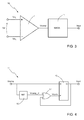
- Figure 3 shows a comparator device 10 comprising a comparator 1, for example, of the type described with reference to Figure 1 , and a protection circuit 11, which is configured for receiving at input a digital signal, possibly with noise signals superimposed thereon (such as, for example, the impulsive noise 5 shown in Figure 2b ) and generating a useful output signal Vout similar to the signal at input but without noise switchings 6 in rapid succession with respect to one another.
- a comparator device 10 comprising a comparator 1, for example, of the type described with reference to Figure 1 , and a protection circuit 11, which is configured for receiving at input a digital signal, possibly with noise signals superimposed thereon (such as, for example, the impulsive noise 5 shown in Figure 2b ) and generating a useful output signal Vout similar to the signal at input but without noise switchings 6 in rapid succession with respect to one another.
- the useful output signal Vout generated by the protection circuit 11 has the same period and the same duty cycle as the comparison signal Vcomp at input to the protection circuit 11. Particular cases, where the duty cycle and/or the period of the useful output signal Vout could vary with respect to the ones of the comparison signal Vcomp, will be illustrated more fully in what follows.
- the protection circuit 11 receives at input the comparison signal Vcomp generated by the comparator 1, which, as has been described with reference to Figures 2a, 2b , can be subject to noise switchings 6, and generates at output a useful output signal Vout without noise switchings 6 in rapid succession with respect to one another.
- the protection circuit 11, in fact, operates a masking of the comparison signal Vcomp generated by the comparator 1 in order to prevent noise switchings 6 present in the comparison signal Vcomp from causing respective noise switchings in the useful output signal Vout.
- the masking is activated when a first switching of the comparison signal Vcomp is detected and has a masking duration Tmask.
- the protection circuit 11 In normal operation, i.e., in the absence of masking, the protection circuit 11 is substantially transparent and the comparison signal Vcomp is reproduced at output, creating the useful output signal Vout.
- a first switching edge of the comparison signal Vcomp causes a respective switching of the useful output signal Vout.
- the masking is activated.
- the protection circuit 11 decouples its own input from its own output, and maintains, for a time equal to the masking duration Tmask, the useful output signal Vout at the last value acquired by the comparison signal Vcomp following upon detection of the switching edge, irrespective of possible further switching edges by the comparison signal Vcomp. In this way, during the entire masking duration Tmask, any possible noise switchings 6 of the comparison signal Vcomp do not generate respective switchings of the useful output signal Vout.
- the masking step terminates, the useful output signal Vout on the output of the protection circuit 11 reproduces again the comparison signal Vcomp, and the protection circuit 11 remains in a wait state for a subsequent switching edge of the comparison signal Vcomp.
- the subsequent switching edge in a way similar to what is described regarding the first switching edge, controls a respective switching of the useful output signal Vout and hence, with a delay given by the electronic components used, the masking is activated again.
- the protection circuit 11 decouples again its own input from its own output and maintains the useful output signal Vout at the last value acquired for the entire masking duration Tmask.
- the duration of Tmask is conditioned by the duration of the period of the signal at input to the protection circuit 11 (the comparison signal Vcomp in the embodiment described).
- Tmask Tmask ⁇ T SEM
- T SEM is the shortest semi-period of the period of the analog input signal Vin (equal, but for noise switchings 6, to the shortest semi-period of the period of the comparison signal Vcomp).
- the comparison signal Vcomp has a duty cycle of 50% (semi-periods of equal duration)
- the masking duration Tmask as being lower than half of the period of the analog input signal Vin, it is possible to obtain an adequate protection from possible noise, in any case guaranteeing detection of the switching edge (rising/falling edge) of the comparison signal Vcomp (assuming absence of noise in the interval comprised between the end of the masking duration Tmask and the switching edge of the comparison signal Vcomp).
- the protection circuit 11 comprises: a memory element, for example a flip-flop 15, configured for accepting on a data input D the comparison signal Vcomp and on an enable input E an enable signal and for generating on an output Q the useful output signal Vout; a delay element 16, configured for accepting at input the comparison signal Vcomp and for generating at output a delayed digital input signal Vcomp_rit, in particular delayed by a time equal to the desired masking duration Tmask; and a logic gate 17, more precisely an XOR gate, configured for accepting on a first input the delayed digital input signal Vcomp_rit and on a second input the useful output signal Vout generated by the flip-flop 15, and for generating at output a masking control signal Vcontr, of a digital type, supplied on the enable input E of the flip-flop 15.
- a memory element for example a flip-flop 15, configured for accepting on a data input D the comparison signal Vcomp and on an enable input E an enable signal and for generating on an output Q the useful output signal Vout
- a delay element 16 configured for
- the output Vcomp_rit of the delay element 16 and the output Vout of the flip-flop 15 control, through the XOR logic gate 17, operation of the flip-flop 15 itself.
- the masking control signal Vcontr when the masking control signal Vcontr is low (logic 0), the useful output signal Vout corresponds to the comparison signal Vcomp, but for a delay introduced by the flip-flop 15, and hence the masking is de-activated; instead, when the masking control signal Vcontr is high (logic 1), the masking is active and the flip-flop 15 maintains the useful output signal Vout at the value defined by the state previously acquired.
- Figure 5 shows a circuit scheme of the delay element 16, according to a possible embodiment.
- the delay element 16 comprises a charge pump 20, of a known type, connected to the input of the delay element and configured for being controlled by the comparison signal Vcomp.
- the charge pump 20 is shown according to a schematic representation, and comprises: a first current generator 22, connected to a supply voltage Vdd (of an appropriate value, for example comprised between 2 V and 5 V) and configured for generating a current Iup; a second current generator 23, connected to a ground terminal GND (for example set at 0 V) and configured for generating a current Idw, for example equal to 2 ⁇ Iup; and a switch 24, for example an N-channel MOSFET, which is sent into conduction or inhibition by means of the comparison signal Vcomp and has a first conduction terminal connected to the first current generator 22 and a second conduction terminal connected to the second current generator 23.
- Vdd supply voltage
- GND for example set at 0 V
- a switch 24 for example an N-channel MOSFET, which is sent into conduction or inhibition by means of the comparison signal Vcomp and has a first conduction terminal connected to the first current generator 22 and a second conduction terminal connected to the second current generator 23.
- the first conduction terminal of the electronic switch 24 is moreover connected to a first pin of a capacitor 25, which is in turn connected via a second pin to the ground terminal GND.
- the first conduction terminal of the electronic switch 24 is connected to an inverter 26.
- Further inverters 27, for example of the same type as the inverter 26, can optionally be connected in series to the inverter 26 to obtain at output from the delay block a signal with faster rising and falling edges.
- the output of the series of the inverters 26 and 27 forms the delayed digital input signal Vcomp_rit.
- the masking duration Tmask is hence intrinsically defined by the charging/discharging time of the capacitor 25 upon reaching of the inversion threshold voltage Vth of the inverter 26 (and of the further inverters 27, if present).
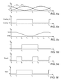
- Figures 6a-6f and 7a-7d show an example of variation in time of the signals involved during masking. The masking intervenes always, both in the presence of glitches or other noise and in the absence thereof.
- Figures 6a-6f show a case in which masking intervenes in the absence of glitch and noise in general. An example of masking in the presence of glitches and noise is described with reference to Figures 7a-7d .
- Figure 6a shows the analog input signal Vin according to a differential representation, showing the voltage signals Vin P and Vin N present on respective non-inverting and inverting inputs of the comparator 1 of Figure 3 .
- the analog input signal Vin is of a sinusoidal type, ideally comprised in the range of voltage values (-Vs, ..., +Vs).
- analog input signal Vin can be of a different type from the one shown and can be comprised in any range of voltage values, according to the need.
- Figure 6b shows the comparison signal Vcomp generated at output from the comparator 1 of Figure 3 .
- the comparison signal Vcomp is a square wave, with duty cycle of 50% and frequency equal to the frequency of the analog input signal Vin.
- Figure 6b shows an ideal representation in which the signal Vcomp takes a value of logic zero Vcomp L and a value of logic one Vcomp H . It is also in this case clear that the logic zero and the logic one can be implemented by means of appropriate voltage values, according to the need.
- the value of effective voltage of Vcomp H must be such as to send the switch 24 into conduction and enable a progressive discharging of the capacitor 25. For example, it is possible to associate to the logic one the value of 3.5 V.
- the capacitor 25 starts to discharge at the temporal instant t1 (the voltage Vc across it decreases) and is completely discharged at the temporal instant tc1.
- the masking control signal Vcontr on the enable input E of the flip-flop 15 (the reversed signal is not shown in the figure), in such a way that a high masking control signal Vcontr will control the flip-flop 15 in a memory state.
- the useful output signal Vout on the output Q maintains the last logic value acquired irrespective of the value assumed by the comparison signal Vcomp on the data input D .
- the output Q of the latch preserves its own state irrespective of the value assumed by the comparison signal Vcomp on the input D .
- the signal on the output Q assumes the logic value of the comparison signal Vcomp present on the input D .
- the flip-flop 15 During the interval t1-tR, i.e., as long as the masking control signal Vcontr is maintained at the high logic value, the flip-flop 15 generates a useful output signal Vout having a high logic value, irrespective of the variations of the comparison signal Vcomp.
- the delayed digital input signal Vcomp_rit assumes a high logic value
- the masking control signal Vcontr assumes a low logic value.
- the output of the flip-flop 15 will consequently switch at the next switching of the comparison signal Vcomp.
- the comparison signal Vcomp switches at the temporal instant t2 from the high logic level to the low logic level, assuming the value Vcomp L and causing a respective switching of the useful output signal Vout.
- Vcomp L must be such as to send the switch 24 into inhibition and enable discharging of the capacitor 25 (for example, Vcomp L can be equal to 0 V).
- Vcomp L can be equal to 0 V.
- the capacitor 25 starts to charge at the temporal instant t2 (the voltage Vc across it increases) and is completely charged at the temporal instant tc2.
- the delayed digital input signal Vcomp_rit generated by the delay circuit 16 assumes a low logic value.
- the masking control signal Vcontr generated by the logic gate 17, of an XOR type is again a signal with high logic value, in so far as, in the time interval, the useful output signal Vout has a low logic value, whilst the signal Vcomp_rit has a high logic value.
- the flip-flop 15 generates at output a low logic value, independent of the variations of the comparison signal Vcomp.
- the flip-flop 15 is driven into a memory state and maintains the useful output signal Vout fixed at the last logic value assumed (in this case, a low logic value).
- the voltage Vc reaches the inversion threshold voltage Vth of the inverter 26 (and of the inverters 27, if present) and the delayed digital input signal Vcomp_rit assumes a low logic value. Consequently, also the masking control signal Vcontr assumes a low logic value, terminating masking.
- the useful output signal Vout generated by the flip-flop 15 can consequently switch at the next switching of the comparison signal Vcomp.
- the masking duration Tmask is, consequently, defined by the time of discharging and charging of the capacitor 25, i.e., by the time intervals t1-tR and t2-tD, respectively.
- Figure 6f shows the useful output signal Vout, generated by the flip-flop 15 according to what is described with reference to Figures 6a-6e .
- the useful output signal Vout is uncoupled from the comparison signal Vcomp during the time intervals t1-tR and t2-tD, and follows the variations of the comparison signal Vcomp outside of the time intervals.
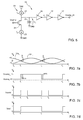
- Figures 7a-7d show an example in which noise (for example, marked differential glitches) present on the input voltage signal Vin ( Figure 7a ) cause undesirable switchings of the input digital signal ( Figure 7b ) generated by the comparator 1 of Figure 3 .
- noise for example, marked differential glitches
- the protection circuit 11 operates as already described with reference to Figures 6a-6f .
- the masking duration Tmask is longer than the duration of the noise disturbances that arise following upon passage through the zero of the analog input signal Vin.
- the useful output signal Vout is insensitive to the presence of the noise and coincides with the useful output signal Vout that would be obtained in the absence of noise on the analog input signal Vin.
- the masking duration Tmask depends upon the current Iup, upon the value of capacitance C of the capacitor 25, and upon the inversion threshold voltage Vth.
- the latter in particular, can vary as a function of the value of supply voltage Vdd (for example, in the case of an inverter of a CMOS type, the inversion threshold voltage Vth is equal to Vdd/2).
- a way for sizing the various parameters that determine Tmask as a function of formulas (3) and (4) can be the following.
- Vcomp the frequency value of the maximum comparison signal Vcomp envisaged (period of the minimum comparison signal Vcomp)
- reasonably small nominal values of current Iup and Idw are considered, to limit consumption.
- a nominal value of capacitance C of the capacitor 25 is defined.
- the comparator device 10 can, for example, be used in circuits for driving micro-electromechanical structures, where a mobile mass must be energized and continuously kept in oscillation at a natural resonance pulsation, such as, for example, a microintegrated gyroscope. This must not, however, be considered as being in any way limiting in so far as the invention can be exploited in all the cases where it is advantageous to mask noise signals superimposed on a digital signal generated by a converter, by a comparator, or other device.
- a microintegrated system 100 for example, a microintegrated gyroscope, comprises a microstructure 102, obtained using MEMS technology, a driving device 103, and a reading device 104, housed on a support (not shown).
- the microstructure 102 is provided with an actuation system 5 and an inertial sensor 6, which includes respective mobile masses.
- the actuation system 5 comprises a driving mass 107, oscillating about a position of rest according to a degree of freedom of its own, whilst the inertial sensor 6 comprises a detection mass 108, mechanically connected to the driving mass 107 by means of springs (not illustrated herein) so as to be set in motion when the driving mass 107 is energized.
- the detection mass 108 is relatively mobile with respect to the driving mass 107 according to a further degree of freedom.
- the driving device 103 comprises, for example, an amplifier 109, a derivative stage 110, a variable-gain-amplifier (VGA) circuit 111, a controller 112, and a phase-locked-loop (PLL) circuit 113.
- VGA variable-gain-amplifier
- PLL phase-locked-loop
- the PLL circuit 113 has inputs connected to the outputs of the derivative stage 110 through the comparator device 10, and an output 113a, connected to a timing input 112c of the controller 112.
- the comparator device 10 receives at input an analog input signal Vin at output from the derivative stage, for example, a sinusoidal signal with a frequency of 4.6 kHz, and supplies at output to the PLL circuit 113 an output signal Vout, of a binary type (in particular a square-wave signal that assumes two logic values, a high one and a low one).
- the output signal Vout has here the function of first clock signal CK.
- the first clock signal CK together with a second clock signal CK 90 , out of phase by 90° and picked up on the output of the PLL circuit 113, is supplied to the reading device 104 in order to synchronize the operations of driving and reading of the microstructure 102.
- the driving device 103 operates on the total gain and phase of the feedback-control loop 105 so as to maintain the driving mass 107 constantly in oscillation at a resonance pulsation ⁇ R .
- noise signals could in fact generate a plurality of undesirable switchings on the first clock signal CK; in this case, the PLL circuit 113 could lose synchronism, unlocking from the frequency of oscillation of the driving mass 107, which would hence be energized at a frequency different from the resonance frequency.
- the masking control signal Vcontr (and hence the masking of possible switchings of the comparison signal Vcomp) is activated by any change of logic state of the comparison signal Vcomp, i.e., by the passage from a low logic value to a high logic value and vice versa, irrespective of whether the change of logic state is caused by an event of noise present on the analog input signal Vin or by an effective variation of logic state.
- the noises are generally systematic glitches, such as to cause a temporal shift of the comparison signal Vcomp. This causes a systematic advance of the useful output signal Vout, which comes to find itself no longer in phase with the analog input signal Vin. Since the temporal shift is systematic, it can be calibrated digitally to enable the synchronism to be restored.
- the useful output signal Vout is supplied at input to a PLL circuit.
- a possible jitter noise can be in any case compensated for by the PLL circuit itself, which, on the basis of its own specifications, is able to recover the synchronism.
- the present invention enables elimination of problems of synchronism deriving from multiple switchings in rapid succession deriving from noise signals, especially in the case of glitches that arise in switched-capacitor architectures.
- the masking of the noise is carried out without the need for digital signals generated outside the comparator circuit 10 by a purposely provided digital circuit dedicated to control of the masking.
- the delay circuit 16 and the logic gate 17 can be provided in a totally digital integrated form, for example, by implementing a software comprising a counter block (not shown), configured for receiving at input the comparison signal Vcomp and supplying at output the masking control signal Vcontr, having a rising edge controlled by the rising edge of the comparison signal Vcomp and a falling edge controlled by the counter block itself.
- a software comprising a counter block (not shown), configured for receiving at input the comparison signal Vcomp and supplying at output the masking control signal Vcontr, having a rising edge controlled by the rising edge of the comparison signal Vcomp and a falling edge controlled by the counter block itself.
Landscapes
- Physics & Mathematics (AREA)
- Engineering & Computer Science (AREA)
- Computer Hardware Design (AREA)
- Computing Systems (AREA)
- General Engineering & Computer Science (AREA)
- Mathematical Physics (AREA)
- Nonlinear Science (AREA)
- Manipulation Of Pulses (AREA)
- Amplifiers (AREA)
- Noise Elimination (AREA)
- Analogue/Digital Conversion (AREA)
Abstract
Description
- The present invention relates to a device and a method of protection from noise that is present in a digital signal.
Figure 1 shows a continuous-timedifferential comparator 1 of a known type. Thecomparator 1 is configured for accepting at input an analog input signal Vin and supplying at output a comparison signal Vcomp, of a binary type, which can assume a high logic value VcompH (logic 1) or a low logic value VcompL (logic 0) on the basis of the analog input signal Vin. - In greater detail, the
comparator 1 receives on an inverting input and on a non-inverting input the analog input signal Vin. In use, thecomparator 1 compares the voltage signal VinP present on the non-inverting input with the voltage signal VinN present on the inverting input, and supplies at output the comparison signal Vcomp according to the following formula (1):
- It is clear that, whereas the voltage signals VinP and VinN are analog signals, the comparison signal Vcomp is of a binary type, since it assumes alternatively the high logic value VcompH and the low logic value VcompL.
- Defining the analog input signal Vin as differential signal Vin = VinP - VinN the equations of formula (1) can be expressed according to the following formula (2):

-
Figure 2a shows an analog input signal Vin of a sinusoidal type, represented showing the voltage signals VinP and VinN at the inputs of thecomparator 1, which oscillates assuming the voltage values (-Vs, ..., +Vs), whilstFigure 2b shows the comparison signal Vcomp, which assumes the logic value VcompH = 1 or VcompL = 0 according to the equation expressed by the formula (2). - The analog input signal Vin generally comprises a useful signal component and a noise component. The noise component may in turn be broken down into an electronic-noise component and in an impulsive-noise component, for example caused by capacitive couplings, often associated to switched-capacitor circuit structures, which cause brief and sudden voltage peaks (referred to as "glitches"), generally of a periodic type, when there occurs switching of digital signals present the switched-capacitor structures.
- As is shown in the
figures 2a and 2b , the presence of numerous events of impulsive noise 5 (for example, glitches) in rapid succession with respect to one another in the analog input signal Vin can causerespective noise switchings 6 of spurious and undesirable noise, which also occur in rapid succession with respect to one another, of the comparison signal Vcomp of thecomparator 1. - The
noise switchings 6 can cause improper operation of a system in which thecomparator 1 is implemented. For instance, if the output voltage signal of thecomparator 1 is used as input of a phase-locked-loop (PLL) circuit, for example of a feedback circuit that operates synchronously, the noise switchings could jeopardize proper operation of the PLL circuit and consequently of the entire system. - The aim of the present invention is to provide a device and a method of protection from noise that is present in a digital signal that will overcome the drawbacks of the prior art.
- According to the present invention, a device and a method of protection from noise that is present in a digital signal are provided, as defined in
claims 1 and 9. - For a better understanding of the invention, a preferred embodiment thereof is now described, purely by way of nonlimiting example and with reference to the attached drawings, wherein:
-
Figure 1 shows a comparator of a known type; -
Figures 2a and 2b show, respectively, a differential signal at input to and at output from the comparator ofFigure 1 ; -
Figure 3 shows a comparator device according to the present invention; -
Figure 4 shows a circuit for protection from noise signals of the comparator device ofFigure 3 ; -
Figure 5 shows a circuit for delay of signals within the protection circuit ofFigure 4 ; -
Figures 6a-6f show waveforms of signals at input to, present within, and generated by the comparator device ofFigure 3 , in the absence of noise signals; -
Figures 7a-7d show waveforms of signals at input to, present within, and generated by the comparator device ofFigure 3 in the presence of noise signals; and -
Figure 8 shows a micro-electromechanical system in which the comparator device ofFigure 3 can be implemented. -
Figure 3 shows acomparator device 10 comprising acomparator 1, for example, of the type described with reference toFigure 1 , and aprotection circuit 11, which is configured for receiving at input a digital signal, possibly with noise signals superimposed thereon (such as, for example, theimpulsive noise 5 shown inFigure 2b ) and generating a useful output signal Vout similar to the signal at input but withoutnoise switchings 6 in rapid succession with respect to one another. - In general, the useful output signal Vout generated by the
protection circuit 11 has the same period and the same duty cycle as the comparison signal Vcomp at input to theprotection circuit 11. Particular cases, where the duty cycle and/or the period of the useful output signal Vout could vary with respect to the ones of the comparison signal Vcomp, will be illustrated more fully in what follows. - In greater detail, the
protection circuit 11 receives at input the comparison signal Vcomp generated by thecomparator 1, which, as has been described with reference toFigures 2a, 2b , can be subject tonoise switchings 6, and generates at output a useful output signal Vout withoutnoise switchings 6 in rapid succession with respect to one another. Theprotection circuit 11, in fact, operates a masking of the comparison signal Vcomp generated by thecomparator 1 in order to preventnoise switchings 6 present in the comparison signal Vcomp from causing respective noise switchings in the useful output signal Vout. The masking is activated when a first switching of the comparison signal Vcomp is detected and has a masking duration Tmask. - In normal operation, i.e., in the absence of masking, the
protection circuit 11 is substantially transparent and the comparison signal Vcomp is reproduced at output, creating the useful output signal Vout. A first switching edge of the comparison signal Vcomp causes a respective switching of the useful output signal Vout. Then, following upon the first switching edge, with a minimum delay, intrinsic to the electronic components used (generally of a few nanoseconds), the masking is activated. In this case, theprotection circuit 11 decouples its own input from its own output, and maintains, for a time equal to the masking duration Tmask, the useful output signal Vout at the last value acquired by the comparison signal Vcomp following upon detection of the switching edge, irrespective of possible further switching edges by the comparison signal Vcomp. In this way, during the entire masking duration Tmask, anypossible noise switchings 6 of the comparison signal Vcomp do not generate respective switchings of the useful output signal Vout. - At the end of the masking duration Tmask, the masking step terminates, the useful output signal Vout on the output of the
protection circuit 11 reproduces again the comparison signal Vcomp, and theprotection circuit 11 remains in a wait state for a subsequent switching edge of the comparison signal Vcomp. The subsequent switching edge, in a way similar to what is described regarding the first switching edge, controls a respective switching of the useful output signal Vout and hence, with a delay given by the electronic components used, the masking is activated again. Theprotection circuit 11 decouples again its own input from its own output and maintains the useful output signal Vout at the last value acquired for the entire masking duration Tmask. - The duration of Tmask is conditioned by the duration of the period of the signal at input to the protection circuit 11 (the comparison signal Vcomp in the embodiment described).
- For example, it is possible to size the masking duration Tmask according to the following formula (3):

where TSEM is the shortest semi-period of the period of the analog input signal Vin (equal, but fornoise switchings 6, to the shortest semi-period of the period of the comparison signal Vcomp). - Assuming that the comparison signal Vcomp has a duty cycle of 50% (semi-periods of equal duration), by sizing the masking duration Tmask as being lower than half of the period of the analog input signal Vin, it is possible to obtain an adequate protection from possible noise, in any case guaranteeing detection of the switching edge (rising/falling edge) of the comparison signal Vcomp (assuming absence of noise in the interval comprised between the end of the masking duration Tmask and the switching edge of the comparison signal Vcomp).
- In the case where the duty cycle of the comparison signal Vcomp is different from 50%, detection of the switching edge is guaranteed by sizing the masking duration Tmask in such a way that it is shorter than the semi-period of the comparison signal Vcomp having shortest duration.
-
Figure 4 shows a possible embodiment of theprotection circuit 11. According to this embodiment, theprotection circuit 11 comprises: a memory element, for example a flip-flop 15, configured for accepting on a data input D the comparison signal Vcomp and on an enable input E an enable signal and for generating on an output Q the useful output signal Vout; adelay element 16, configured for accepting at input the comparison signal Vcomp and for generating at output a delayed digital input signal Vcomp_rit, in particular delayed by a time equal to the desired masking duration Tmask; and alogic gate 17, more precisely an XOR gate, configured for accepting on a first input the delayed digital input signal Vcomp_rit and on a second input the useful output signal Vout generated by the flip-flop 15, and for generating at output a masking control signal Vcontr, of a digital type, supplied on the enable input E of the flip-flop 15. - In this way, the output Vcomp_rit of the
delay element 16 and the output Vout of the flip-flop 15 control, through theXOR logic gate 17, operation of the flip-flop 15 itself. In fact, when the masking control signal Vcontr is low (logic 0), the useful output signal Vout corresponds to the comparison signal Vcomp, but for a delay introduced by the flip-flop 15, and hence the masking is de-activated; instead, when the masking control signal Vcontr is high (logic 1), the masking is active and the flip-flop 15 maintains the useful output signal Vout at the value defined by the state previously acquired. -
Figure 5 shows a circuit scheme of thedelay element 16, according to a possible embodiment. - The
delay element 16 comprises acharge pump 20, of a known type, connected to the input of the delay element and configured for being controlled by the comparison signal Vcomp. - The
charge pump 20 is shown according to a schematic representation, and comprises: a firstcurrent generator 22, connected to a supply voltage Vdd (of an appropriate value, for example comprised between 2 V and 5 V) and configured for generating a current Iup; a secondcurrent generator 23, connected to a ground terminal GND (for example set at 0 V) and configured for generating a current Idw, for example equal to 2·Iup; and aswitch 24, for example an N-channel MOSFET, which is sent into conduction or inhibition by means of the comparison signal Vcomp and has a first conduction terminal connected to the firstcurrent generator 22 and a second conduction terminal connected to the secondcurrent generator 23. - The first conduction terminal of the
electronic switch 24 is moreover connected to a first pin of acapacitor 25, which is in turn connected via a second pin to the ground terminal GND. In addition, the first conduction terminal of theelectronic switch 24 is connected to aninverter 26.Further inverters 27, for example of the same type as theinverter 26, can optionally be connected in series to theinverter 26 to obtain at output from the delay block a signal with faster rising and falling edges. The output of the series of theinverters - In use, when the comparison voltage Vcomp switches to VcompL, the
electronic switch 24 is sent into inhibition, and thecapacitor 25 is charged by the current Iup, until the voltage on thecapacitor 25 reaches a voltage value Vc ≈ Vdd. Instead, when the comparison voltage Vcomp switches to VcompH, theelectronic switch 24 is sent into conduction, and thecapacitor 25 discharges with a current given by Idw - Iup, until the voltage on thecapacitor 25 reaches a voltage value Vc ≈ GND. - Masking starts when the
capacitor 25 starts to charge/discharge, and lasts until the voltage Vc by increasing or decreasing crosses the inversion threshold of the inverter 26 (and of thefurther inverters 27, if present). Consequently, masking is activated both on the rising edge and on the falling edge of the comparison voltage Vcomp. According to the embodiment shown, the masking duration Tmask is defined by the value of capacitance C of thecapacitor 25, by the current Iup, and by the value of the inversion threshold voltage Vth of theinverter 26, according to the following formula (4):
- The masking duration Tmask is hence intrinsically defined by the charging/discharging time of the
capacitor 25 upon reaching of the inversion threshold voltage Vth of the inverter 26 (and of thefurther inverters 27, if present).Figures 6a-6f and7a-7d show an example of variation in time of the signals involved during masking. The masking intervenes always, both in the presence of glitches or other noise and in the absence thereof.Figures 6a-6f show a case in which masking intervenes in the absence of glitch and noise in general. An example of masking in the presence of glitches and noise is described with reference toFigures 7a-7d . - With reference to
Figures 6a-6f and7a-7d , the intrinsic delays of the flip-flop 15 and of thelogic gate 17 are not considered for simplicity of description. -
Figure 6a shows the analog input signal Vin according to a differential representation, showing the voltage signals VinP and VinN present on respective non-inverting and inverting inputs of thecomparator 1 ofFigure 3 . In the example ofFigure 6a , the analog input signal Vin is of a sinusoidal type, ideally comprised in the range of voltage values (-Vs, ..., +Vs). - It is clear that the analog input signal Vin can be of a different type from the one shown and can be comprised in any range of voltage values, according to the need.
-
Figure 6b shows the comparison signal Vcomp generated at output from thecomparator 1 ofFigure 3 . The comparison signal Vcomp is a square wave, with duty cycle of 50% and frequency equal to the frequency of the analog input signal Vin. Given that the comparison signal Vcomp is a digital signal,Figure 6b shows an ideal representation in which the signal Vcomp takes a value of logic zero VcompL and a value of logic one VcompH. It is also in this case clear that the logic zero and the logic one can be implemented by means of appropriate voltage values, according to the need. In what follows, when not otherwise specified, the analog input signal Vin is understood as input differential signal Vin = VinP - VinN at input to thecomparator 1 ofFigure 3 . - With joint reference to
Figures 6a and 6b , in the time interval t0 - t1, the analog input signal Vin is negative. Consequently, with reference to formula (2), the comparison signal Vcomp has a low logic value, equal to VcompL = 0. With reference toFigure 5 , theswitch 24 is sent into inhibition, and thecapacitor 25, by charging, develops a voltage across its terminals equal to Vc ≈ Vdd.Figure 6c shows the evolution of the voltage Vc on the capacitor 25 (assumed, for simplicity of description, already partially charged at the instant t0). - At the temporal instant t1, the analog input signal Vin is equal to zero (VinP = VinN) and, at the temporal instants subsequent to t1, the analog input signal Vin assumes a positive value. The comparison signal Vcomp switches from the low logic level at the high logic level, assuming the value VcompH = 1. In particular, with joint reference to
Figure 5 , the value of effective voltage of VcompH must be such as to send theswitch 24 into conduction and enable a progressive discharging of thecapacitor 25. For example, it is possible to associate to the logic one the value of 3.5 V. - As is shown in
Figure 6c , thecapacitor 25 starts to discharge at the temporal instant t1 (the voltage Vc across it decreases) and is completely discharged at the temporal instant tc1. - When, at a temporal instant tR comprised between the temporal instants t1 and tc1, as the voltage Vc across the
capacitor 25 discharges it reaches the inversion threshold voltage Vth of the inverter 26 (and of theinverter 27, if present), and thedelay circuit 16 generates at output (Figure 6d ) the delayed digital input signal Vcomp_rit. During the time interval t1-tR the signals at input to thelogic gate 17 do not present the same logic value. In fact, as shown inFigures 6b, 6d and 6f , the comparison signal Vcomp with high logic value causes at the temporal instant t1 a switching to a high logic value of the useful output signal Vout, whilst the signal Vcomp_rit maintains a low logic value. The inputs of thelogic gate 17, of an XOR type, consequently assume a different logic value. The masking control signal Vcontr generated by thelogic gate 17 is hence a signal with high logic value. - The masking control signal Vcontr on the enable input E of the flip-flop 15 (the reversed signal is not shown in the figure), in such a way that a high masking control signal Vcontr will control the flip-
flop 15 in a memory state. The useful output signal Vout on the output Q maintains the last logic value acquired irrespective of the value assumed by the comparison signal Vcomp on the data input D. - Next, when the masking control signal Vcontr present on the activation input E of the flip-
flop 15 is maintained at the high logic level, the output Q of the latch preserves its own state irrespective of the value assumed by the comparison signal Vcomp on the input D. Instead, when the masking control signal Vcontr on the input E switches to the low logic level, the signal on the output Q assumes the logic value of the comparison signal Vcomp present on the input D. - During the interval t1-tR, i.e., as long as the masking control signal Vcontr is maintained at the high logic value, the flip-
flop 15 generates a useful output signal Vout having a high logic value, irrespective of the variations of the comparison signal Vcomp. - When, at the temporal instant tR, the delayed digital input signal Vcomp_rit assumes a high logic value, the masking control signal Vcontr assumes a low logic value. The output of the flip-
flop 15 will consequently switch at the next switching of the comparison signal Vcomp. - At the temporal instant t2, the analog input signal Vin is again equal to zero (VinP = VinN), whereas at the temporal instants subsequent to t2 it assumes a negative value. The comparison signal Vcomp switches at the temporal instant t2 from the high logic level to the low logic level, assuming the value VcompL and causing a respective switching of the useful output signal Vout.
- With reference to
Figure 5 , the value VcompL must be such as to send theswitch 24 into inhibition and enable discharging of the capacitor 25 (for example, VcompL can be equal to 0 V). As is shown inFigure 6c , thecapacitor 25 starts to charge at the temporal instant t2 (the voltage Vc across it increases) and is completely charged at the temporal instant tc2. - When the voltage Vc across the
capacitor 25 by charging reaches the inversion threshold voltage Vth of the inverter 26 (and of theinverters 27 if present), in a temporal instant tD comprised between the temporal instants t2 and tc2, the delayed digital input signal Vcomp_rit generated by thedelay circuit 16 assumes a low logic value. - In the time interval comprised between t2 and tD the masking control signal Vcontr generated by the
logic gate 17, of an XOR type, is again a signal with high logic value, in so far as, in the time interval, the useful output signal Vout has a low logic value, whilst the signal Vcomp_rit has a high logic value. - Next, during the interval t2-tD, the flip-
flop 15 generates at output a low logic value, independent of the variations of the comparison signal Vcomp. The flip-flop 15 is driven into a memory state and maintains the useful output signal Vout fixed at the last logic value assumed (in this case, a low logic value). - At the temporal instant tD the voltage Vc reaches the inversion threshold voltage Vth of the inverter 26 (and of the
inverters 27, if present) and the delayed digital input signal Vcomp_rit assumes a low logic value. Consequently, also the masking control signal Vcontr assumes a low logic value, terminating masking. The useful output signal Vout generated by the flip-flop 15 can consequently switch at the next switching of the comparison signal Vcomp. - The masking duration Tmask is, consequently, defined by the time of discharging and charging of the
capacitor 25, i.e., by the time intervals t1-tR and t2-tD, respectively.Figure 6f shows the useful output signal Vout, generated by the flip-flop 15 according to what is described with reference toFigures 6a-6e . The useful output signal Vout is uncoupled from the comparison signal Vcomp during the time intervals t1-tR and t2-tD, and follows the variations of the comparison signal Vcomp outside of the time intervals. - Hence, at the temporal instant t3 the input differential signal Vin is again equal to zero, and the steps described with reference to
Figures 6a-6f are repeated. -
Figures 7a-7d show an example in which noise (for example, marked differential glitches) present on the input voltage signal Vin (Figure 7a ) cause undesirable switchings of the input digital signal (Figure 7b ) generated by thecomparator 1 ofFigure 3 . - The
protection circuit 11 operates as already described with reference toFigures 6a-6f . - As may be noted from
Figure 7c , which shows the masking control signal Vcontr, the masking duration Tmask is longer than the duration of the noise disturbances that arise following upon passage through the zero of the analog input signal Vin. In this way, the useful output signal Vout is insensitive to the presence of the noise and coincides with the useful output signal Vout that would be obtained in the absence of noise on the analog input signal Vin. - As expressed by formula (4), the masking duration Tmask depends upon the current Iup, upon the value of capacitance C of the
capacitor 25, and upon the inversion threshold voltage Vth. The latter, in particular, can vary as a function of the value of supply voltage Vdd (for example, in the case of an inverter of a CMOS type, the inversion threshold voltage Vth is equal to Vdd/2). To obtain a masking duration Tmask equal both to the positive switching edge of the comparison signal Vcomp and to the negative switching edge, it is preferable to guarantee that thecapacitor 25 will be charged/discharged completely. - A way for sizing the various parameters that determine Tmask as a function of formulas (3) and (4) can be the following. There are considered the voltage value of the maximum threshold voltage Vth (defined in the design stage, for example, in the case of a CMOS inverter in which Vth = Vdd/2, considering the maximum value of supply voltage Vdd) and the frequency value of the maximum comparison signal Vcomp envisaged (period of the minimum comparison signal Vcomp), for which in fact the charging (and discharging) time of the
capacitor 25 is longer. In addition, reasonably small nominal values of current Iup and Idw are considered, to limit consumption. Finally, on the basis of the above considerations, a nominal value of capacitance C of thecapacitor 25 is defined. - The
comparator device 10 can, for example, be used in circuits for driving micro-electromechanical structures, where a mobile mass must be energized and continuously kept in oscillation at a natural resonance pulsation, such as, for example, a microintegrated gyroscope. This must not, however, be considered as being in any way limiting in so far as the invention can be exploited in all the cases where it is advantageous to mask noise signals superimposed on a digital signal generated by a converter, by a comparator, or other device. - For example, the
comparator device 10 can be used in a microintegrated gyroscope of the type described in the patent No.US 7,305,880 and described in brief in what follows with reference toFigure 8 . Here, amicrointegrated system 100, for example, a microintegrated gyroscope, comprises amicrostructure 102, obtained using MEMS technology, adriving device 103, and areading device 104, housed on a support (not shown). Themicrostructure 102 is provided with anactuation system 5 and aninertial sensor 6, which includes respective mobile masses. More precisely, theactuation system 5 comprises a drivingmass 107, oscillating about a position of rest according to a degree of freedom of its own, whilst theinertial sensor 6 comprises adetection mass 108, mechanically connected to the drivingmass 107 by means of springs (not illustrated herein) so as to be set in motion when the drivingmass 107 is energized. In addition, thedetection mass 108 is relatively mobile with respect to the drivingmass 107 according to a further degree of freedom. - The
driving device 103 comprises, for example, anamplifier 109, aderivative stage 110, a variable-gain-amplifier (VGA)circuit 111, acontroller 112, and a phase-locked-loop (PLL)circuit 113. - The
PLL circuit 113 has inputs connected to the outputs of thederivative stage 110 through thecomparator device 10, and anoutput 113a, connected to atiming input 112c of thecontroller 112. Thecomparator device 10 receives at input an analog input signal Vin at output from the derivative stage, for example, a sinusoidal signal with a frequency of 4.6 kHz, and supplies at output to thePLL circuit 113 an output signal Vout, of a binary type (in particular a square-wave signal that assumes two logic values, a high one and a low one). - The output signal Vout has here the function of first clock signal CK. The first clock signal CK, together with a second clock signal CK90, out of phase by 90° and picked up on the output of the
PLL circuit 113, is supplied to thereading device 104 in order to synchronize the operations of driving and reading of themicrostructure 102. - In addition, the driving
device 103 operates on the total gain and phase of the feedback-control loop 105 so as to maintain the drivingmass 107 constantly in oscillation at a resonance pulsation ωR. - It is thus clear how maintaining the synchronism for the operations of driving and reading of the
microstructure 102 is essential for proper operation of themicrointegrated gyroscope 100. As described with reference toFigures 2a and 2b , noise signals could in fact generate a plurality of undesirable switchings on the first clock signal CK; in this case, thePLL circuit 113 could lose synchronism, unlocking from the frequency of oscillation of the drivingmass 107, which would hence be energized at a frequency different from the resonance frequency. - It is evident from the description of the
protection circuit 11 that the masking control signal Vcontr (and hence the masking of possible switchings of the comparison signal Vcomp) is activated by any change of logic state of the comparison signal Vcomp, i.e., by the passage from a low logic value to a high logic value and vice versa, irrespective of whether the change of logic state is caused by an event of noise present on the analog input signal Vin or by an effective variation of logic state. - In the presence of marked noise on the analog input signal Vin, previous to the passage through the zero of the analog input signal Vin, (for example, with reference to
Figure 7b , prior to the temporal instant t1 and/or t2 but outside the masking interval tR-t1 and/or tD-t2), it can happen that the masking will be activated by an error switching generated by a noise and not by the effective switching of the signal. - The noises are generally systematic glitches, such as to cause a temporal shift of the comparison signal Vcomp. This causes a systematic advance of the useful output signal Vout, which comes to find itself no longer in phase with the analog input signal Vin. Since the temporal shift is systematic, it can be calibrated digitally to enable the synchronism to be restored.
- With particular reference to the gyroscope of
Figure 8 , the useful output signal Vout is supplied at input to a PLL circuit. In this case, a possible jitter noise can be in any case compensated for by the PLL circuit itself, which, on the basis of its own specifications, is able to recover the synchronism. - Alternatively, additional compensation methods and circuits can be implemented in order to compensate for the variation of the duty cycle.
- From an examination of the characteristics of the device and of the method of protection from noise of a digital signal provided according to the present invention the advantages that it enables emerge clearly.
- For example, the present invention enables elimination of problems of synchronism deriving from multiple switchings in rapid succession deriving from noise signals, especially in the case of glitches that arise in switched-capacitor architectures.
- In addition, the masking of the noise is carried out without the need for digital signals generated outside the
comparator circuit 10 by a purposely provided digital circuit dedicated to control of the masking. - Finally, it is clear that modifications and variations may be made to the device and method of protection from noise for a digital signal described and illustrated herein, without thereby departing from the sphere of protection of the present invention, as defined in the annexed claims. For example, the
delay circuit 16 and thelogic gate 17 can be provided in a totally digital integrated form, for example, by implementing a software comprising a counter block (not shown), configured for receiving at input the comparison signal Vcomp and supplying at output the masking control signal Vcontr, having a rising edge controlled by the rising edge of the comparison signal Vcomp and a falling edge controlled by the counter block itself.
Claims (15)
- A method of protection from noise for a digital signal (Vcomp) generated by a comparator (1), comprising the steps of:- generating an output signal (Vout), which switches from a first logic state to a second logic state at a first switching of logic state of the digital signal (Vcomp);- detecting a change from the first logic state to the second logic state of the output signal (Vout); and- inhibiting further switchings of the output signal (Vout) for a first time interval after the change from the first logic state to the second logic state.
- The method according to claim 1, wherein the inhibiting step comprises maintaining the output signal (Vout) at the second logic level during the first time interval (Tmask).
- The method according to claim 1 or claim 2, comprising, after the first time interval, the steps of:- switching the output signal (Vout) from the second logic state to the first logic state upon detection of a second switching of logic state of the digital signal (Vcomp);- detecting a change from the second logic state to the first logic state of the output signal (Vout); and- inhibiting further switchings of the output signal (Vout) for a second time interval after the change from the second logic state to the first logic state.
- The method according to claim 3, wherein the step of inhibiting further switchings of the output signal (Vout) for a second time interval comprises maintaining the output signal (Vout) at the first logic level during said second time interval (Tmask).
- The method according to claim 3 or claim 4, wherein said digital signal is a periodic signal having a semi-period, said first and second time intervals (Tmask) having a duration shorter than said semi-period of the digital signal (Vcomp).
- The method according to any one of claims 3-5, wherein the step of detecting a change from the first logic state to the second logic state of the output signal comprises:- collecting said output signal (Vout);- generating a verification signal (Vcomp_rit) delayed with respect to said digital signal;- comparing said output signal (Vout) with the verification signal (Vcomp_rit); and- generating an inhibition-control signal (Vcontr), which enables a further change of logic state of said output signal only after detection of a switching of logic state of said verification signal.
- The method according to claim 6, wherein said step of generating a verification signal (Vcomp_rit) comprises:- sending said digital signal (Vcomp) to a control input of a switch (24);- issuing a command, respectively, for charging and discharging of a capacitor (25) by the switch (24); and- enabling generation of the verification signal (Vcomp_rit) upon reaching of a value of charge of the capacitor (25).
- The method according to claim 6 or claim 7, wherein said comparison step comprises carrying out an XOR logic operation between the output signal (Vout) and the verification signal (Vcomp_rit).
- A comparator device (10) comprising a comparator (1), configured for generating a digital signal (Vcomp), and a protection circuit (11), the protection circuit (11) comprising:- signal-generating means (15), configured for generating an output signal (Vout) that switches from a first logic state to a second logic state upon detection of switchings of logic state of the digital signal (Vcomp);- state-change detection means (16, 17), configured for detecting a change from the first logic state to the second logic state of the output signal (Vout); and- switching-inhibition means (15), configured for inhibiting switching of the output signal (Vout) for a time interval (Tmask) after said change from the first logic state to the second logic state.
- The device according to claim 9, wherein said switching-inhibition means (15) comprise memory means (15), configured for maintaining the output signal (Vout) in said second logic state during said time interval (Tmask).
- The device according to claim 9 or claim 10, wherein said switching-detection means (16, 17) comprise:- delay means (16), configured for receiving the digital signal (Vcomp) and generating a verification signal delayed with respect to the digital signal; and- comparison means (17), configured for comparing said output signal (Vout) with the verification signal (Vcomp_rit), and generating an inhibition-control signal (Vcontr) that enables a further change of logic state of said output signal only after detection of a switching of logic state of said verification signal.
- The device according to claim 11, wherein the memory means comprise a flip-flop (15) of a D type, having an enable input (E) configured for receiving the control signal (Vcontr), a data input (D) configured for receiving the digital signal (Vcomp), and an output (Q) configured for generating the output signal (Vout); and the comparison means (17) comprise an XOR logic gate, having a first input connected to an output of the delay means (16), a second input connected to the output of the flip-flop (15), and an output connected to the enable input (E) of the flip-flop (15).
- The device according to claim 11 or 12, wherein the delay means (16) comprise:- a charge pump (20), including a switch (24) having a control terminal connected to an output of the comparator, a first conduction terminal connected to a first line at a reference potential (Vdd) and a second conduction terminal connected to a second line at a reference potential (GND);- a capacitor (25) having a first pin connected to the first conduction terminal of the switch and a second pin connected to the second line at a reference potential (GND); and- at least one threshold element (26), having an input connected to the first pin of the capacitor (25) and an output connected to the comparison means (17).
- A resonant micro-electromechanical system comprising: a microstructure (102), having a mass (107) free to oscillate; and a driving device (103), coupled to said mass (107) for keeping said mass (107) in oscillation, wherein said driving device (103) comprises:- a reading differential amplifier (109);- an actuation and control stage (111, 112, 113), including a PLL circuit (113) and configured for driving said mass (107); and- a comparator device (10) according to any one of claims 9-13, connected between said differential read amplifier (109) and the PLL circuit (113) of said actuation and control stage (111, 112, 113).
- The micro-electromechanical system according to claim 14 constituting a gyroscope.
Applications Claiming Priority (1)
| Application Number | Priority Date | Filing Date | Title |
|---|---|---|---|
| IT000334A ITTO20090334A1 (en) | 2009-04-28 | 2009-04-28 | DEVICE AND METHOD OF PROTECTION FROM DISTURBANCES FOR A DIGITAL SIGNAL |
Publications (1)
| Publication Number | Publication Date |
|---|---|
| EP2246981A1 true EP2246981A1 (en) | 2010-11-03 |
Family
ID=41786055
Family Applications (1)
| Application Number | Title | Priority Date | Filing Date |
|---|---|---|---|
| EP10161176A Withdrawn EP2246981A1 (en) | 2009-04-28 | 2010-04-27 | Digital noise protection circuit and method |
Country Status (4)
| Country | Link |
|---|---|
| US (3) | US8164357B2 (en) |
| EP (1) | EP2246981A1 (en) |
| JP (1) | JP2011019212A (en) |
| IT (1) | ITTO20090334A1 (en) |
Families Citing this family (16)
| Publication number | Priority date | Publication date | Assignee | Title |
|---|---|---|---|---|
| US8314685B2 (en) * | 2007-08-27 | 2012-11-20 | Texas Instruments Incorporated | Data detector for UHF RFID tags |
| US8727217B2 (en) | 2007-08-27 | 2014-05-20 | Texas Instruments Incorporated | Data detector for UHF RFID tags |
| US7759171B2 (en) * | 2007-08-28 | 2010-07-20 | Spansion Llc | Method and structure of minimizing mold bleeding on a substrate surface of a semiconductor package |
| ITTO20090334A1 (en) | 2009-04-28 | 2010-10-29 | St Microelectronics Srl | DEVICE AND METHOD OF PROTECTION FROM DISTURBANCES FOR A DIGITAL SIGNAL |
| JP5776927B2 (en) * | 2011-03-28 | 2015-09-09 | ソニー株式会社 | Information processing apparatus and method, and program |
| JP5778099B2 (en) * | 2012-08-24 | 2015-09-16 | 株式会社日本自動車部品総合研究所 | Receiver circuit |
| US10309782B2 (en) | 2015-04-07 | 2019-06-04 | Analog Devices, Inc. | Quality factor estimation for resonators |
| US9735759B1 (en) | 2016-04-11 | 2017-08-15 | Motorola Solutions, Inc. | Systems and methods for mitigating noise in an electronic device |
| FR3068548A1 (en) * | 2017-06-28 | 2019-01-04 | Stmicroelectronics (Grenoble 2) Sas | NON-OSCILLATING COMPARATOR |
| US10578435B2 (en) | 2018-01-12 | 2020-03-03 | Analog Devices, Inc. | Quality factor compensation in microelectromechanical system (MEMS) gyroscopes |
| US11041722B2 (en) | 2018-07-23 | 2021-06-22 | Analog Devices, Inc. | Systems and methods for sensing angular motion in the presence of low-frequency noise |
| US10491235B1 (en) | 2018-12-21 | 2019-11-26 | Motorola Solutions, Inc. | Devices and methods for multi-mode sample generation |
| US10985783B1 (en) * | 2019-09-26 | 2021-04-20 | Nanya Technology Corporation | Correction device |
| FR3102621B1 (en) | 2019-10-24 | 2022-01-14 | St Microelectronics Grenoble 2 | Voltage comparator |
| JP2022067812A (en) | 2020-10-21 | 2022-05-09 | セイコーエプソン株式会社 | Display device operation method and display device |
| CN113765347B (en) * | 2021-09-03 | 2024-03-12 | 江苏润石科技有限公司 | DC-DC circuit structure and method for eliminating burr effect |
Citations (8)
| Publication number | Priority date | Publication date | Assignee | Title |
|---|---|---|---|---|
| JPS62155615A (en) * | 1985-11-25 | 1987-07-10 | Mitsubishi Electric Corp | Frequency division circuit |
| JPH05218822A (en) * | 1991-12-04 | 1993-08-27 | Nec Corp | Pulse shaping circuit |
| JPH06209245A (en) * | 1993-01-12 | 1994-07-26 | Nec Ic Microcomput Syst Ltd | Delay circuit |
| EP0632590A1 (en) * | 1993-06-30 | 1995-01-04 | Harris Corporation | Glitch suppressor circuit and method |
| JPH08242153A (en) * | 1995-03-02 | 1996-09-17 | Nitsuko Corp | Latch circuit |
| JPH10190413A (en) * | 1996-12-25 | 1998-07-21 | Sharp Corp | Oscillation stop detection circuit |
| EP1294123A1 (en) * | 2001-09-18 | 2003-03-19 | Broadcom Corporation | Linear phase detector for high-speed clock and data recovery |
| US7305880B2 (en) | 2004-08-03 | 2007-12-11 | Stmicroelectronics S.R.L. | Resonant micro-electro-mechanical system with analog driving |
Family Cites Families (7)
| Publication number | Priority date | Publication date | Assignee | Title |
|---|---|---|---|---|
| US5537062A (en) * | 1995-06-07 | 1996-07-16 | Ast Research, Inc. | Glitch-free clock enable circuit |
| US6535057B2 (en) * | 2000-05-29 | 2003-03-18 | Stmicroelectronics Ltd. | Programmable glitch filter |
| DE10142679A1 (en) * | 2001-08-31 | 2003-04-03 | Infineon Technologies Ag | driver circuit |
| JP2004080721A (en) * | 2002-06-21 | 2004-03-11 | Shimada Phys & Chem Ind Co Ltd | Signal receiving circuit |
| JP3934504B2 (en) * | 2002-08-01 | 2007-06-20 | 松下電器産業株式会社 | Binary circuit |
| US6842044B1 (en) * | 2003-10-23 | 2005-01-11 | International Business Machines Corporation | Glitch-free receivers for bi-directional, simultaneous data bus |
| ITTO20090334A1 (en) * | 2009-04-28 | 2010-10-29 | St Microelectronics Srl | DEVICE AND METHOD OF PROTECTION FROM DISTURBANCES FOR A DIGITAL SIGNAL |
-
2009
- 2009-04-28 IT IT000334A patent/ITTO20090334A1/en unknown
-
2010
- 2010-04-27 US US12/768,276 patent/US8164357B2/en active Active
- 2010-04-27 JP JP2010102336A patent/JP2011019212A/en active Pending
- 2010-04-27 EP EP10161176A patent/EP2246981A1/en not_active Withdrawn
-
2012
- 2012-02-29 US US13/408,956 patent/US8519736B2/en active Active
-
2013
- 2013-07-25 US US13/951,312 patent/US9083338B2/en active Active
Patent Citations (8)
| Publication number | Priority date | Publication date | Assignee | Title |
|---|---|---|---|---|
| JPS62155615A (en) * | 1985-11-25 | 1987-07-10 | Mitsubishi Electric Corp | Frequency division circuit |
| JPH05218822A (en) * | 1991-12-04 | 1993-08-27 | Nec Corp | Pulse shaping circuit |
| JPH06209245A (en) * | 1993-01-12 | 1994-07-26 | Nec Ic Microcomput Syst Ltd | Delay circuit |
| EP0632590A1 (en) * | 1993-06-30 | 1995-01-04 | Harris Corporation | Glitch suppressor circuit and method |
| JPH08242153A (en) * | 1995-03-02 | 1996-09-17 | Nitsuko Corp | Latch circuit |
| JPH10190413A (en) * | 1996-12-25 | 1998-07-21 | Sharp Corp | Oscillation stop detection circuit |
| EP1294123A1 (en) * | 2001-09-18 | 2003-03-19 | Broadcom Corporation | Linear phase detector for high-speed clock and data recovery |
| US7305880B2 (en) | 2004-08-03 | 2007-12-11 | Stmicroelectronics S.R.L. | Resonant micro-electro-mechanical system with analog driving |
Also Published As
| Publication number | Publication date |
|---|---|
| US8519736B2 (en) | 2013-08-27 |
| US20130307581A1 (en) | 2013-11-21 |
| US8164357B2 (en) | 2012-04-24 |
| US9083338B2 (en) | 2015-07-14 |
| JP2011019212A (en) | 2011-01-27 |
| US20120153987A1 (en) | 2012-06-21 |
| US20100271067A1 (en) | 2010-10-28 |
| ITTO20090334A1 (en) | 2010-10-29 |
Similar Documents
| Publication | Publication Date | Title |
|---|---|---|
| US8519736B2 (en) | Digital noise protection circuit and method | |
| JP2011223375A (en) | Oscillator circuit | |
| US7656206B2 (en) | Phase-locked loop circuit | |
| US8786375B2 (en) | Runtime compensated oscillator | |
| US20040177290A1 (en) | Frequency detection circuit and data processing apparatus | |
| US6867657B2 (en) | Relaxation oscillator | |
| US6518848B2 (en) | Oscillation stop detection circuit | |
| CN118295857A (en) | Clock circuit | |
| CN103140764B (en) | The method and apparatus that frequency is determined | |
| JP2009529823A (en) | Pulse shaping circuit for crystal oscillator | |
| US9257976B2 (en) | Semiconductor device with touch sensor circuit | |
| CN103187034B (en) | Signal synchronization system and signal synchronization method for driving light-emitting diodes | |
| JP2005252447A (en) | Lock detection circuit and method | |
| JP2005301388A (en) | Semiconductor integrated circuit | |
| JP3392278B2 (en) | Oscillator | |
| JP3774038B6 (en) | Power-on reset signal generation circuit | |
| JP3774038B2 (en) | Power-on reset signal generation circuit | |
| JP2005184113A (en) | Serial link circuit | |
| JP4353791B2 (en) | Pulse generator | |
| JP6522956B2 (en) | Clock generator, clock generation module, and clock source selection method | |
| JP2757827B2 (en) | Microcomputer | |
| JPH118538A (en) | Repeat signal stop detection circuit | |
| JP4283717B2 (en) | Delay compensation circuit | |
| JP2009044402A (en) | Delay pulse generation circuit | |
| JP2006319446A (en) | Frequency-dividing circuit |
Legal Events
| Date | Code | Title | Description |
|---|---|---|---|
| PUAI | Public reference made under article 153(3) epc to a published international application that has entered the european phase |
Free format text: ORIGINAL CODE: 0009012 |
|
| AK | Designated contracting states |
Kind code of ref document: A1 Designated state(s): AT BE BG CH CY CZ DE DK EE ES FI FR GB GR HR HU IE IS IT LI LT LU LV MC MK MT NL NO PL PT RO SE SI SK SM TR |
|
| AX | Request for extension of the european patent |
Extension state: AL BA ME RS |
|
| 17P | Request for examination filed |
Effective date: 20110503 |
|
| RAP1 | Party data changed (applicant data changed or rights of an application transferred) |
Owner name: STMICROELECTRONICS SRL |
|
| 17Q | First examination report despatched |
Effective date: 20131030 |
|
| STAA | Information on the status of an ep patent application or granted ep patent |
Free format text: STATUS: THE APPLICATION IS DEEMED TO BE WITHDRAWN |
|
| 18D | Application deemed to be withdrawn |
Effective date: 20131101 |