JP5776927B2 - Information processing apparatus and method, and program - Google Patents
Information processing apparatus and method, and program Download PDFInfo
- Publication number
- JP5776927B2 JP5776927B2 JP2011069925A JP2011069925A JP5776927B2 JP 5776927 B2 JP5776927 B2 JP 5776927B2 JP 2011069925 A JP2011069925 A JP 2011069925A JP 2011069925 A JP2011069925 A JP 2011069925A JP 5776927 B2 JP5776927 B2 JP 5776927B2
- Authority
- JP
- Japan
- Prior art keywords
- attack
- strength
- security
- unit
- time
- Prior art date
- Legal status (The legal status is an assumption and is not a legal conclusion. Google has not performed a legal analysis and makes no representation as to the accuracy of the status listed.)
- Active
Links
Images


Classifications
-
- G—PHYSICS
- G06—COMPUTING; CALCULATING OR COUNTING
- G06F—ELECTRIC DIGITAL DATA PROCESSING
- G06F21/00—Security arrangements for protecting computers, components thereof, programs or data against unauthorised activity
- G06F21/50—Monitoring users, programs or devices to maintain the integrity of platforms, e.g. of processors, firmware or operating systems
- G06F21/55—Detecting local intrusion or implementing counter-measures
- G06F21/554—Detecting local intrusion or implementing counter-measures involving event detection and direct action
-
- G—PHYSICS
- G06—COMPUTING; CALCULATING OR COUNTING
- G06F—ELECTRIC DIGITAL DATA PROCESSING
- G06F21/00—Security arrangements for protecting computers, components thereof, programs or data against unauthorised activity
- G06F21/70—Protecting specific internal or peripheral components, in which the protection of a component leads to protection of the entire computer
- G06F21/71—Protecting specific internal or peripheral components, in which the protection of a component leads to protection of the entire computer to assure secure computing or processing of information
- G06F21/72—Protecting specific internal or peripheral components, in which the protection of a component leads to protection of the entire computer to assure secure computing or processing of information in cryptographic circuits
Description
本技術は、情報処理装置及び方法、並びにプログラムに関し、特に、処理速度を維持したまま、セキュリティレベルを向上させることができる、情報処理装置及び方法、並びにプログラムに関する。 The present technology relates to an information processing apparatus, method, and program, and more particularly, to an information processing apparatus, method, and program that can improve the security level while maintaining the processing speed.
近年、IC(Integrated Circuit)カードに含まれるICチップに対する能動攻撃が脅威となっている。能動攻撃とは、悪意のある第三者が、ICカードにレーザー光を照射させる等して、本来の通常動作とは異なる動作を人為的かつ強制的にICチップに実行させ、秘密情報を入手しようとすることをいう。 In recent years, active attacks against IC chips included in IC (Integrated Circuit) cards have become a threat. Active attack means that a malicious third party causes the IC chip to artificially and forcibly execute an operation different from the normal operation by irradiating the IC card with laser light, etc. to obtain confidential information It means trying.
このような能動攻撃の代表的な1つとして、DFA(Differential Fault Analysis)攻撃が存在する。DFAとは、悪意のある第三者が、本来の通常動作とは異なる動作を人為的かつ強制的にICチップに実行させ、その結果得られる異常な演算結果と、予め入手しておいた通常動作による正常な演算結果とを比較することによって、秘密情報を入手しようとすることをいう。 A typical example of such an active attack is a DFA (Differential Fault Analysis) attack. DFA is a malicious third party that artificially and forcibly executes an operation different from the normal normal operation on the IC chip. This means that secret information is to be obtained by comparing with a normal calculation result by operation.
このようなDFA等の能動攻撃に対して秘密情報を保護する従来の手法としては、暗号演算等の重要な処理を検算することで、通常動作とは異なる動作(すなわち、能動攻撃による異常動作)を検出する手法が存在する(特許文献1参照)。 As a conventional method for protecting confidential information against such active attacks such as DFA, operations that differ from normal operations (ie, abnormal operations due to active attacks) are verified by checking important processes such as cryptographic operations. There exists a technique for detecting the above (see Patent Document 1).
しかしながら、近年では、強いレーザー光を短周期で照射できる装置が製品化されている。このような装置による能動攻撃に対して、従来の手法を適用して秘密情報を守るためには、検算回数やセキュリティチェックをさらに増す等してセキュリティレベルを向上させる必要がある。一方、セキュリティレベルの向上は、ICチップの処理速度の低下を招く。このように、従来の手法を適用すると、セキュリティレベルと、ICチップの処理速度との間にトレードオフの関係が生じてしまい、ICチップの処理速度を維持したまま、セキュリティレベルを向上させることは非常に困難である。 However, in recent years, devices that can irradiate intense laser light in a short period have been commercialized. In order to protect the secret information by applying the conventional technique against the active attack by such an apparatus, it is necessary to improve the security level by increasing the number of verifications and the security check. On the other hand, the improvement of the security level causes a decrease in the processing speed of the IC chip. In this way, when the conventional method is applied, there is a trade-off relationship between the security level and the processing speed of the IC chip, and it is not possible to improve the security level while maintaining the processing speed of the IC chip. It is very difficult.
本技術は、このような状況に鑑みてなされたものであり、処理速度を維持したまま、セキュリティレベルを向上させることができるようにしたものである。 The present technology has been made in view of such a situation, and is capable of improving the security level while maintaining the processing speed.
本技術の一側面の情報処理装置は、攻撃を検出する攻撃検出部と、前記攻撃検出部により攻撃が検出される毎に、セキュリティ対策の強度を段階的に上げるために、重要処理を所定の回数だけ実行し、前記所定の回数分の前記重要処理の結果を比較して一致するか否かを判断する検算処理における前記所定の回数をインクリメントし、所定の条件が満たされる毎に、前記セキュリティ対策の強度を段階的に下げるために前記検算処理における前記所定の回数をデクリメントする強度調整部とを備える。 An information processing apparatus according to an aspect of the present technology includes an attack detection unit that detects an attack, and performs an important process in order to increase the strength of security measures step by step each time an attack is detected by the attack detection unit . The security processing is executed for the predetermined number of times, the result of the important processing for the predetermined number of times is compared to determine whether or not they match , and the predetermined number of times is incremented. An intensity adjusting unit that decrements the predetermined number of times in the verification process in order to lower the intensity of the countermeasure stepwise;
前記強度調整部は、前記セキュリティ対策の強度を上げるために、さらに、タイミングジッタの挿入量の増加、ダミー演算の挿入、通常モードに戻るまでの時間の増加、または規定処理の成功回数の増加のうち、少なくとも1つを行うことができる。 In order to increase the strength of the security measure , the strength adjustment unit further increases the amount of insertion of timing jitter, inserts dummy operations, increases the time until returning to the normal mode, or increases the number of times of successful prescribed processing. At least one of them can be performed .
前記強度調整部は、前記所定の条件として、前記攻撃検出部により攻撃が検出されてから所定時間が経過したという条件、または規定処理の実行が成功したという条件の少なくとも一方が満たされた場合、前記検算の回数をデクリメントすることができる。 The strength adjustment unit, as the predetermined condition, when at least one of a condition that a predetermined time has elapsed since the attack was detected by the attack detection unit , or a condition that the prescribed process has been successfully executed, is satisfied, The number of checks can be decremented.
前記攻撃検出部による攻撃の検出後にコンデンサを充電する充放電部と、前記充放電部により放電されつつある前記コンデンサの電荷量と、所定の閾値とを比較する電荷量検出部とをさらに備え、前記所定時間は、電荷量が前記所定の閾値となるまでの前記コンデンサの放電時間とすることができる。 A charge / discharge unit that charges a capacitor after detection of an attack by the attack detection unit; and a charge amount detection unit that compares a charge amount of the capacitor being discharged by the charge / discharge unit with a predetermined threshold value; The predetermined time can be a discharge time of the capacitor until the amount of charge reaches the predetermined threshold.
前記強度調整部は、前記セキュリティ対策の強度を上げる対象を、前記攻撃検出部により攻撃が検出された関数とすることができる。 The strength adjustment unit may set a target for increasing the strength of the security countermeasure as a function in which an attack is detected by the attack detection unit.
前記強度調整部は、前記セキュリティ対策の強度を上げる対象を、前記攻撃検出部により攻撃が検出された関数が実行されている前記情報処理装置の構成要素が実行するすべての関数とすることができる。 The strength adjusting unit can set targets for increasing the strength of the security countermeasures as all functions executed by the components of the information processing apparatus on which the function in which the attack is detected by the attack detecting unit is executed. .
本技術の一側面の情報処理方法及びプログラムは、上述した本技術の一側面の情報処理装置に対応する方法及びプログラムである。 An information processing method and program according to one aspect of the present technology are a method and program corresponding to the information processing apparatus according to one aspect of the present technology described above.
本技術の一側面においては、攻撃が検出され、攻撃が検出される毎に、セキュリティ対策の強度を段階的に上げるために、重要処理を所定の回数だけ実行し、前記所定の回数分の前記重要処理の結果を比較して一致するか否かを判断する検算処理における前記所定の回数がインクリメントされ、また、所定の条件が満たされる毎に、前記セキュリティ対策の強度を段階的に下げるために前記検算処理における前記所定の回数がデクリメントされる。 In one aspect of the present technology, an attack is detected, and each time an attack is detected, in order to gradually increase the strength of the security countermeasure , the important process is executed a predetermined number of times, and the predetermined number of times In order to reduce the strength of the security countermeasure step by step each time the predetermined number of times in the verification process for comparing the results of the important processes to determine whether or not they match is incremented and the predetermined condition is satisfied The predetermined number of times in the verification process is decremented.
以上のごとく、本技術によれば、処理速度を維持したまま、セキュリティレベルを向上させることができる。 As described above, according to the present technology, it is possible to improve the security level while maintaining the processing speed.
[本技術の概要]
はじめに、本技術の理解を容易なものとすべく、その概略について説明する。
[Overview of this technology]
First, the outline will be described in order to facilitate understanding of the present technology.
本技術に属するICカードは、能動攻撃(以下、攻撃と略称する)を検出する毎に、セキュリティレベル(以下、セキュリティ対策の強度とも称する)を段階的に上げる。例えば、セキュリティ対策として暗号演算の検算が採用されているICカードは、攻撃を検出する毎に、検算回数を1回ずつ増やしていく。すると、攻撃者がICカードに対する攻撃を試みる毎に、当該ICカードのセキュリティ対策の強度は加速度的に上がるので、当該ICカードに対する攻撃の成功率は飛躍的に低下していく。 Each time an IC card belonging to the present technology detects an active attack (hereinafter abbreviated as an attack), the security level (hereinafter also referred to as the strength of a security measure) is increased stepwise. For example, an IC card that uses cryptographic computation verification as a security measure increases the number of verifications by one each time an attack is detected. Then, every time an attacker attempts an attack on the IC card, the strength of the security measures for the IC card increases at an accelerated rate, and the success rate of the attack against the IC card decreases dramatically.
一方、セキュリティ対策の強度を上げたままでは、処理速度が低下して、ユーザビリティが損なわれるおそれがある。したがって、本技術に属するICカードは、ユーザビリティを維持するために、攻撃検出後に所定の条件が満たされると、セキュリティ対策の強度を段階的に下げる。例えば、攻撃検出後に所定時間が経過した場合や、既定処理の実行に成功した場合、当該ICカードは、検算回数を1回ずつ減らしていく。すると、所定の条件が満たされる毎に処理速度はもとの速度に近づくので、ユーザビリティが維持される。 On the other hand, if the strength of the security measures is increased, the processing speed may decrease and usability may be impaired. Therefore, in order to maintain usability, the IC card belonging to the present technology gradually reduces the strength of security measures when a predetermined condition is satisfied after an attack is detected. For example, when a predetermined time elapses after the attack is detected or when the predetermined process is successfully executed, the IC card decreases the number of verifications by one. Then, every time a predetermined condition is satisfied, the processing speed approaches the original speed, so that usability is maintained.
このように、ICカードにつき、セキュリティ対策の強度を段階的に調整することにより、処理速度を維持したまま、セキュリティレベルを向上させることができる。 In this way, by adjusting the strength of security measures stepwise for an IC card, the security level can be improved while maintaining the processing speed.
以下、本技術の4つの実施形態(以下、それぞれ第1実施形態乃至第4実施形態と称する)について、次の順序で説明する。
1.第1実施形態(セキュリティ対策として検算回数を段階的に調整する例)
2.第2実施形態(複数のセキュリティ対策の強度を段階的に調整する例)
3.第3実施形態(セキュリティ対策の強度を段階的に調整する関数を限定する例)
4.第4実施形態(セキュリティ対策の強度を段階的に調整する箇所を限定する例)
Hereinafter, four embodiments of the present technology (hereinafter referred to as first to fourth embodiments, respectively) will be described in the following order.
1. First embodiment (example of adjusting the number of verifications step by step as a security measure)
2. Second Embodiment (Example in which the strengths of a plurality of security measures are adjusted in stages)
3. Third embodiment (example of limiting a function for adjusting the strength of security measures step by step)
4). Fourth Embodiment (Example in which locations where the strength of security measures is adjusted in stages are limited)
<1.第1実施形態>
[ICカードの構成例]
図1は、ICカードに含まれるICチップの構成例を示すブロック図である。
<1. First Embodiment>
[Configuration example of IC card]
FIG. 1 is a block diagram illustrating a configuration example of an IC chip included in an IC card.
ICチップ11は、センサ21、RAM(Random Access Memory)22、EEPROM(Electrically Erasable and Programmable Read Only Memory)23、ROM(Read Only Memory)24、暗号エンジン25、乱数発生器26、I/O(Input/Output)27、およびCPU(Central Processing Unit)28が、内部バス29により相互に接続されることにより構成される。
The
センサ21は、ICチップ11への供給電圧、クロック周波数、温度や光といった外部条件等を検出し、検出結果が、予め設定された正常な範囲内にあるか否かを監視する。
The
RAM22は、CPU28が各種の処理を実行する上で必要な各種データなどを適宜記憶する。
The
EEPROM23、ROM24は、各種プログラムを記憶する。
The
暗号エンジン25は、乱数発生器26が発生した乱数を用いて、リーダライタ等の他の装置とICカードとの間で送受信されるデータ、EEPROM23に記憶されたデータ等の各種データをAES(Advanced Encryption Standard)方式で暗号化または復号化する。また、暗号エンジン25は、暗号化又は復号化に際し、鍵の生成、および相互認証等を行う。
The
乱数発生器26は、暗号エンジン25で用いる乱数を発生させ、内部バス29を介して暗号エンジン25に供給する。
The
I/O27は、他の装置とデータの送受信を行う。I/O27は、例えば、リーダライタと電磁波を利用して非接触でデータの送受信を行い、CPU28から内部バス29を介して供給されるデータをリーダライタに送信したり、リーダライタからのデータを受信して内部バス29を介してCPU28等に供給する。
The I /
CPU28は、EEPROM23またはROM24に記録されているプログラムに従って各種の処理を実行する。または、CPU28は、RAM22にロードされたプログラムに従って各種の処理を実行する。RAM22にはまた、CPU28が各種の処理を実行する上で必要なデータなども適宜記憶される。
The
図1に示されるICチップ11は、攻撃を検出する検出手法として、例えば、次の3通りの検出手法を採用することができる。
The
第1の検出手法は、センサ21が外部条件等から攻撃を検出する手法である。上述したように、センサ21は、ICチップ11への供給電圧、クロック周波数、温度や光などの外部条件等を検出し、その検出結果が、予め設定された正常な範囲内にあるか否かを監視する。そして、センサ21は、これらの外部条件等の検出値が異常値を示した場合には、ICチップ11が攻撃を受けたと判断する。
The first detection method is a method in which the
第2の検出手法は、CPU28が重要な処理の検算結果から攻撃を検出する手法である。CPU28は、重要な処理に対しては検算を行い、通常の演算結果と検算の演算結果が一致するかを検証する。そして、CPU28は、通常の演算結果と検算の演算結果が一致しなかった場合には、ICチップ11が攻撃を受けたと判断する。
The second detection method is a method in which the
第3の検出手法は、CPU28が関数の戻り値から攻撃を検出する手法である。CPU28は、予め設定された関数の戻り値が正常であるかを検証する。そして、CPU28は、戻り値が異常な値を示した場合には、ICチップ11が攻撃を受けたと判断する。
The third detection method is a method in which the
なお、第1乃至第3の検出手法は、個別に単体で用いてもよいし、任意の種類の任意の個数の検出手法を組み合わせて用いてもよい。さらに、ここでは説明しない別の検出手法を、単体で、又は、第1乃至第3の検出手法を含む他の検出手法のうち、任意の種類の任意の個数の検出手法と組み合せてもよい。要するに、ICチップ11が攻撃を検出する手法は、ICチップ11に対する攻撃を検出できる手法であれば足り、1以上の任意の種類の任意の個数の手法を適宜組み合わせて用いることができる。
The first to third detection methods may be used individually or in combination with any number of detection methods of any type. Furthermore, another detection method that is not described here may be combined with any number of detection methods of any type among a single detection method or other detection methods including the first to third detection methods. In short, the technique for detecting an attack by the
ICチップ11は、これらの手法により攻撃を検出した場合、攻撃を検出する毎に重要な処理の検算回数のカウント値を1ずつインクリメントすることによって、攻撃が成功してしまう難易度を上げる。以下、検算回数が増やされる重要な処理として、暗号演算が採用された場合を例に説明する。
When detecting an attack by these methods, the
[検算回数を段階的に増やす例]
図2は、暗号演算の検算回数を段階的に増やす例について説明する図である。
[Example of increasing the check count step by step]
FIG. 2 is a diagram for explaining an example in which the number of verifications of cryptographic operations is increased stepwise.
図2の左側の図に示されるように、セキュリティレベル1の時、すなわち攻撃が検出されていない通常時には、ICチップ11は、第1暗号演算を実行した後で、その検算を目的として、第1暗号演算と同様の第2暗号演算を実行する。したがって、セキュリティレベル1の場合、検算回数は1回となる。ICチップ11は、第1暗号演算と第2暗号演算の2つの演算結果を比較する比較処理を実行し、演算結果が一致した場合には攻撃を受けていないと判断し、一致しない場合には攻撃を受けたと判断する。
As shown in the diagram on the left side of FIG. 2, when the security level is 1, that is, in the normal time when no attack is detected, the
換言すると、攻撃者にとってすれは、第1暗号演算と第2暗号演算の両方を攻撃して同一エラーを発生させることができれば、比較処理の結果が一致してしまうので、ICチップ11に攻撃を受けていないと判断させることができる。この場合、ICチップ11に気付かれないうちに秘密情報が攻撃者に入手されてしまう。しかしながら、1回の攻撃のみで、連続して2回の同一エラーを発生させることは困難であるし、また、1回のエラー結果のみから秘密情報が漏洩してしまうことは非常にまれである。このため、通常、攻撃者は、ICチップ11に何度も攻撃を検出されながらも、複数回にわたって攻撃を執拗に繰り返すことになる。
In other words, if an attacker can attack both the first cryptographic operation and the second cryptographic operation to generate the same error, the results of the comparison process will match. It can be judged that it has not received. In this case, secret information is obtained by an attacker before the
そこで、セキュリティレベル1の状態で攻撃が1度検出されると、ICチップ11は、図2の中央の図に示されるように、セキュリティレベルを2にあげて、暗号演算の検算回数を2回に増やす。すなわち、ICチップ11は、第1暗号演算を実行した後で、その検算として、第2暗号演算及び第3暗号演算を行う。そして、ICチップ11は、第1暗号演算乃至第3暗号演算の3つの演算結果を比較する比較処理を実行し、3つの演算結果が全て一致した場合には攻撃を受けていないと判断し、3つの演算結果から選択された2つの演算結果の組み合わせのうち、1つの組み合わせでも一致しない場合には攻撃を受けたと判断する。
Therefore, the attack on the state of the
換言すると、攻撃者にとっては、ICチップ11に攻撃を受けていないと判断させるためには、セキュリティレベル1では、連続して同一エラーを発生させる回数は2回必要があったところ、セキュリティレベル2になると、当該回数は3回に増えることになる。このように、セキュリティレベル1からセキュリティレベル2になると、検算回数が2回から3回に増加し、その結果、攻撃の難易度(すなわち、秘密情報の入手に失敗する確率)が高くなる。
In other words, in order for an attacker to determine that the
さらに、セキュリティレベル2の状態で攻撃が検出されると、ICチップ11は、図2の右側に示されるように、セキュリティレベルを3にあげて、暗号演算の検算回数を3回に増やす。すなわち、ICチップ11は、第1暗号演算を実行した後で、その検算として、第2暗号演算乃至第4暗号演算を行う。そして、ICチップ11は、第1暗号演算乃至第4暗号演算の4つの演算結果を比較する比較処理を実行し、4つの演算結果が全て一致した場合には攻撃を受けていないと判断し、4つの演算結果から選択された2つの演算結果の組み合わせのうち、1つの組み合わせでも一致しない場合には攻撃を受けたと判断する。
Further, when an attack is detected in the state of
換言すると、攻撃者にとっては、ICチップ11に攻撃を受けていないと判断させるためには、セキュリティレベル2では、連続して同一エラーを発生させる回数は3回必要があったところ、セキュリティレベル3になると、当該回数は4回に増えることになる。このように、セキュリティレベル2からセキュリティレベル3になると、検算回数が3回から4回に増加し、その結果、攻撃の難易度(すなわち、秘密情報の入手に失敗する確率)が高くなる。
In other words, in order for an attacker to determine that the
このように、攻撃が検出される毎に、セキュリティレベルが上がり、その分だけ検算回数が増加していくので、その結果、攻撃の難易度が向上し、攻撃者が秘密情報を入手できる確率は低下していく。 In this way, each time an attack is detected, the security level increases, and the number of verifications increases accordingly.As a result, the difficulty of the attack improves, and the probability that the attacker can obtain confidential information is It goes down.
なお、当然のことながら、セキュリティの上昇毎に増加させる検算回数は1回ずつに限定されず、任意の回数を採用することができる。 As a matter of course, the number of verifications to be increased every time security is increased is not limited to one, and any number can be adopted.
一方、検算回数が増加すると、その分だけ、ICチップ11の処理速度が低下する。したがって、ICチップ11は、所定の条件が満たされた場合には検算回数を減らすことで、自己の処理速度の低下を抑制する。ここで、所定の条件として、例えば、次の2通りの条件のうち一方または両者の組み合わせを採用することができる。
On the other hand, when the number of verifications increases, the processing speed of the
第1の条件として、攻撃検出から所定時間が経過したことという条件を採用することができる。すなわち、攻撃検出から所定時間、例えば30分が経過する毎に、第1の条件が満たされたとして検算回数が1回ずつ減らされる。 As the first condition, a condition that a predetermined time has elapsed since the attack detection can be adopted. That is, every time a predetermined time, for example, 30 minutes elapses from the detection of an attack, the number of verifications is decreased by one because the first condition is satisfied.
第2の条件として、既定処理の実行が成功したことという条件を採用することができる。すなわち、規定処理、例えば相互認証処理における相互認証コマンドに従った処理の実行が成功した場合、条件が満たされたとして検算回数が1回減らされる。なお、既定処理としては、相互認証コマンドの実行に限定されず、例えば、検算回数初期化コマンドに従った処理等、その他ICチップ11が行う各種各様の処理を実行することができる。
As the second condition, a condition that the execution of the default process is successful can be adopted. That is, when the execution of the process according to the mutual authentication command in the prescribed process, for example, the mutual authentication process is successful, the number of verifications is reduced by one because the condition is satisfied. Note that the default process is not limited to the execution of the mutual authentication command, and various other processes performed by the
このように、第1の条件や第2の条件といったように、所定の条件が満たされた場合に検算回数を減らすことで、ICチップ11の処理速度の低下を抑制することができる。なお、所定の条件は、上述の第1及び第2の条件に限定されない。
As described above, when the predetermined condition is satisfied, such as the first condition and the second condition, a decrease in the processing speed of the
以下、さらに、このような第1の条件と第2の条件のうち、第1の条件の詳細について説明する。 Hereinafter, the details of the first condition among the first condition and the second condition will be described.
電力が常時供給される装置であれば、当該装置内に搭載されたクロックカウンタに基づいて、所定時間を計時することは容易である。しかしながら、従来のICカードは、リーダライタ等に接近している時にしか電力が供給されないので、所定時間を計測するのは非常に困難であった。 If the device is constantly supplied with electric power, it is easy to measure the predetermined time based on a clock counter mounted in the device. However, since the conventional IC card is supplied with power only when it is close to a reader / writer or the like, it is very difficult to measure a predetermined time.
そこで、本実施形態のICチップ11を搭載したICカードは、内蔵するコンデンサの充放電時間を用いて所定時間を計測することで、第1の条件が採用可能に構成されている。
Therefore, the IC card equipped with the
本実施形態のICカードには、所定時間の計測が可能となるように設計された充放電回路が搭載されている。このような充放電回路を用いた所定時間の計測について図3と図4を用いて説明する。 The IC card according to the present embodiment is equipped with a charge / discharge circuit designed to allow measurement for a predetermined time. Measurement of a predetermined time using such a charge / discharge circuit will be described with reference to FIGS.
[所定時間の計測について]
図3は、本実施形態のICカードに搭載された充放電回路の原理について説明する図である。
[About measurement of a predetermined time]
FIG. 3 is a diagram for explaining the principle of the charge / discharge circuit mounted on the IC card of the present embodiment.
図3Aは、リーダライタ等が接近してコンデンサが充電する場合の充放電回路41の等価回路図である。
FIG. 3A is an equivalent circuit diagram of the charge /
充放電回路41は、コンデンサC、及び抵抗R1,R2により構成されるCR回路である。即ち、コンデンサCと抵抗R2との並列接続のうち、一端が接地され、他端には、入力端が接続される。ICカードがリーダライタ等に接近すると、入力端に電源Erが接続され、当該入力端と抵抗R1の一端とが接続された状態、換言すると、入力端と抵抗R1を介して出力端とを結ぶ仮想スイッチ42がオン状態になったのと等価な状態になる。この場合、リーダライタ等から供給される電力(等価回路上は電源Erから供給される電力)は、コンデンサCの充電に用いられ、その結果、所定の電荷量Qの電荷が蓄えられる。
The charge /
図3Bは、リーダライタ等が離間してコンデンサが放電する場合の充放電回路41の等価回路図である。
FIG. 3B is an equivalent circuit diagram of the charge /
リーダライタ等がICカードから離間すると、図3Bに示すように、入力端と抵抗R1を介して出力端とを結ぶ仮想スイッチ42がオフ状態になったのと等価な状態になる。この場合、コンデンサCに蓄積された所定の電荷量Qの電荷は、出力端側に放電される。
When the reader / writer or the like is separated from the IC card, as shown in FIG. 3B, the
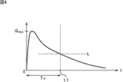
図4は、図3の等価回路のコンデンサCの充放電時の電荷量のタイミングチャートである。 FIG. 4 is a timing chart of the amount of charge during charging / discharging of the capacitor C of the equivalent circuit of FIG.
図4において、縦軸はコンデンサCの電荷量を示し、横軸は時間を示している。 In FIG. 4, the vertical axis indicates the amount of charge of the capacitor C, and the horizontal axis indicates time.
ICカードがリーダライタ等に接近して、仮想スイッチがオン状態に切り替えられた時刻、即ちコンデンサCへの充電が開始した時刻が、基準時刻0とされている。
The time when the IC card approaches the reader / writer or the like and the virtual switch is turned on, that is, the time when charging of the capacitor C is started is defined as the
図4に示すように、基準時刻0にコンデンサCへの充電が開始されると、その後電荷量は即座に上昇し、電荷量Qmaxまで到達する。この段階で、ICカードがリーダライタから離間すると、放電が開始され、電荷量は降下していく。
As shown in FIG. 4, when charging of the capacitor C is started at the
そこで、本実施形態では、放電開始(充電時間は非常に短いので無視すれば時刻0)から電荷量が所定の閾値Lよりも小さくなる時刻t1までの時間Trが、上述した所定時間、例えば30分となるように、充放電回路41が設計される。例えば、充放電回路41はCR回路であるため、コンデンサCの放電の応答特性は一次遅れとみなすことができ、所定の閾値Lを電荷量Qmaxの63%の電荷量とすると、当該閾値Lに到達するまでの時間Trが時定数となるため、時間Trは、コンデンサCの静電容量と抵抗R2の抵抗値の積によって容易に求めることができる。換言すると、設計者は、時間Trが所定時間(例えば30分)となるように、充放電回路41のコンデンサCの静電容量と抵抗R2の抵抗値とを容易に設計することができる。なお、このような閾値Lと所定時間は、例示に過ぎない。
Therefore, in the present embodiment, the time Tr from the start of discharge (
本実施形態のICカードは、このように所定時間を計測可能な充放電回路41を搭載しているので、攻撃が終了した後の検算回数を減らすための第1の条件を採用することができる。即ち、本実施形態のICカードは、充放電回路41により攻撃検出から所定時間が計測されると、第1の条件が満たされたとして、検算回数を1回減らす。
Since the IC card of this embodiment is equipped with the charge /
[CPUの機能的構成例]
図5は、図1のCPU28が有する機能のうち、セキュリティ対策の強度を段階的に調整するための各種機能を実現させるための機能的構成例を示すブロック図である。
[Functional configuration example of CPU]
FIG. 5 is a block diagram showing an example of a functional configuration for realizing various functions for adjusting the strength of security measures in stages among the functions of the
CPU28は、電源起動部61、強度判定部62、メイン処理部63、攻撃検出部64、強度調整部65、充放電部66、動作停止部67、電荷量検出部68、規定処理部69、および規定処理監視部70を有している。
The
電源起動部61は、ICカードがリーダライタ等に接近すると、仮想的に電源を起動させ、ICカードがリーダライタ等から離間すると、仮想的に電源を落とす。ここで、仮想的に電源を起動するとは、充放電回路41を図3Aに示す等価回路として機能させることを意味する。一方、仮想的に電源を落とすとは、充放電回路41を図3Bに示す等価回路として機能させることを意味する。
The
強度判定部62は、現在のICカードに設定されているセキュリティ対策の強度として、検算回数を判定する。
The
メイン処理部63は、ICチップ11が実行すべき処理のコマンドを受信して実行する。
The
攻撃検出部64は、ICチップ11に対する攻撃を検出する。すなわち、攻撃検出部64は、上述した攻撃を検出する第1乃至第3の検出手法のうちの少なくとも1つの検出手法に従って、ICチップ11に対する攻撃を検出する。
The
強度調整部65は、セキュリティ対策の強度の設定の調整、すなわち、検算回数の増減の調整を行う。
The
充放電部66は、図3の充放電回路41に相当し、電源起動部61により仮想的に電源が起動されるとコンデンサCの充電を開始し、電源起動部61により仮想的に電源が落とされるとコンデンサCの放電を開始する。
The charging / discharging
動作停止部67は、CPU28の動作、特にメイン処理部63の動作を停止させる制御を実行する。
The
電荷量検出部68は、充放電部66(すなわち、図3の充放電回路41)のコンデンサCの電荷量を検出し、所定の閾値Lと比較することによって、検算回数を減らすための第1の条件が満たされたか否かを判定する。すなわち、電荷量検出部68は、コンデンサの電荷量が所定の閾値Lよりも小さくなったことを検出したとき、第1の条件が満たされて所定時間が経過したと判断する。
The charge
規定処理部69は、検算回数を減らすための第2の条件として採用される規定処理を実行する。このような規定処理としては、例えば、相互認証コマンドや検算回数初期化コマンドの実行等の処理を採用することができる。
The
規定処理監視部70は、規定処理部69による規定処理の実行が成功したかを監視する。
The regulation
次に、検算回数を減らす所定の条件として、第1の条件、すなわち攻撃検出から所定時間の経過が採用された場合のCPU28が実行する処理(以下、第1のセキュリティ対策強度調整処理と称する)について説明する。
Next, as a predetermined condition for reducing the number of verifications, a process executed by the
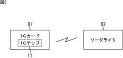
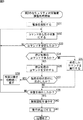
[第1のセキュリティ対策強度調整処理]
図6は、第1のセキュリティ対策強度調整処理が開始される状態を示す図である。
[First security countermeasure strength adjustment process]
FIG. 6 is a diagram illustrating a state in which the first security countermeasure strength adjustment process is started.
ICチップ11を含む非接触型のICカード81は、リーダライタ82に接近すると、電磁誘導によってリーダライタ82から電力の供給を受ける。すると、図7に示される第1のセキュリティ対策強度調整処理が開始される。
When the non-contact
図7は、第1のセキュリティ対策強度調整処理の流れを説明するフローチャートである。 FIG. 7 is a flowchart for explaining the flow of the first security countermeasure strength adjustment process.
ステップS11において、電源起動部61は、リーダライタ82から供給された電力により仮想的に電源を起動する。
In step S <b> 11, the
ステップS12において、強度判定部62は、検算回数が初期値であるかを判定する。なお、検算回数の初期値は、図2を用いて上述したセキュリティレベル1の検算回数である1回が採用されている。
In step S12, the
検算回数が初期値の1回でない場合、ステップS12においてNOであると判定されて、処理はステップS20に進む。なお、ステップS20以降の処理については後述する。 If the number of verifications is not one of the initial values, it is determined as NO in step S12, and the process proceeds to step S20. The processing after step S20 will be described later.
これに対して、検算回数が初期値の1回である場合、ステップS12においてYESであると判定されて、処理はステップS13に進む。すなわち、今までに一度も攻撃が検出されていないか、または攻撃が検出された後に、後述するステップS21で検算回数が初期値に戻された後に攻撃が再検出されていない場合、ステップS12においてYESであると判定されて、処理はステップS13に進む。 On the other hand, when the number of verifications is one of the initial values, it is determined as YES in Step S12, and the process proceeds to Step S13. That is, if no attack has been detected so far, or if an attack has not been detected again after the number of verifications has been returned to the initial value in step S21 described later after the attack has been detected, in step S12 If it is determined as YES, the process proceeds to step S13.
ステップS13において、メイン処理部63は、コマンド待ち受け状態にする。すなわち、メイン処理部63は、リーダライタ82からコマンドが送信されるのを待つ。
In step S13, the
ステップS14において、メイン処理部63は、コマンドを受信したかを判定する。
In step S14, the
コマンドが受信されない場合、ステップS14においてNOであると判定され、処理はステップS13に戻され、それ以降の処理が繰り返される。すなわち、コマンドを受信するまでの間、ステップS13,S14のループ処理が繰り返される。 If the command is not received, it is determined as NO in step S14, the process returns to step S13, and the subsequent processes are repeated. That is, until the command is received, the loop processing of steps S13 and S14 is repeated.
その後、コマンドを受信した場合、ステップS14においてYESであると判定されて、処理はステップS15に進む。 Thereafter, when a command is received, it is determined as YES in Step S14, and the process proceeds to Step S15.
ステップS15において、メイン処理部63は、受信したコマンドを実行する。
In step S15, the
ステップS16において、攻撃検出部64は、攻撃を検出したかを判定する。すなわち、攻撃検出部64は、上述した第1乃至第3の検出手法等により、ICチップ11に対する攻撃の検出を試みる。
In step S16, the
攻撃が検出されていない場合、ステップS16においてNOであると判定され、処理はステップS13に戻され、それ以降の処理が繰り返される。すなわち、攻撃を検出するまでの間、ステップS13乃至S16のループ処理が繰り返される。 If no attack is detected, it is determined as NO in step S16, the process returns to step S13, and the subsequent processes are repeated. That is, the loop process of steps S13 to S16 is repeated until an attack is detected.
その後、攻撃が検出された場合、ステップS16においてYESであると判定されて、処理はステップS17に進む。 Thereafter, when an attack is detected, it is determined as YES in Step S16, and the process proceeds to Step S17.
ステップS17において、強度調整部65は、検算回数を1回増やす。すなわち、強度調整部65は、検算回数を初期値の1回から2回に増やし、セキュリティ対策の強度を上げる。
In step S17, the
ステップS18において、充放電部66は、コンデンサを充電する。すなわち、充放電部66は、攻撃検出からの所定時間の経過を計測するために、コンデンサを充電する
In step S18, the charging / discharging
ステップS19において、動作停止部67は、ICチップ11の動作を停止する。
In step S19, the
これにより、第1のセキュリティ対策強度調整処理は終了する。 Thereby, the first security countermeasure strength adjustment process is completed.
一方、ステップS12において検算回数が初期値でない場合、NOであると判定されて、処理はステップS20に進む。すなわち、攻撃が検出されて検算回数が増やされた後に、ICカードがリーダライタ等に接近されると、再度第1のセキュリティ対策強度調整処理が開始するので、このような場合検算回数は初期値の1回ではないと判定され、即ちステップS12においてNOであると判定されて、処理はステップS20に進む。 On the other hand, when the number of verifications is not the initial value in step S12, it is determined as NO and the process proceeds to step S20. That is, after the attack is detected and the number of verifications is increased, when the IC card approaches a reader / writer or the like, the first security countermeasure strength adjustment process starts again. In such a case, the number of verifications is the initial value. It is determined that it is not once, that is, it is determined as NO in Step S12, and the process proceeds to Step S20.
ステップS20において、電荷量検出部68は、コンデンサの電荷量が閾値Lより小さいかを判定する。すなわち、電荷量検出部68は、攻撃検出から所定時間が経過したかを判定する。
In step S20, the charge
コンデンサの電荷量が閾値Lをまだ下回っていない場合、すなわち、前回の攻撃検出から所定時間が経過していない場合、ステップS20においてNOであると判定されて、処理はステップS13に進む。すなわち、検算回数は減らされないまま、メイン処理が開始される。 If the charge amount of the capacitor has not yet fallen below the threshold value L, that is, if the predetermined time has not elapsed since the previous attack detection, it is determined NO in step S20, and the process proceeds to step S13. That is, the main process is started without reducing the number of verifications.
これに対して、コンデンサの電荷量が閾値Lを下回っている場合、すなわち、前回の攻撃検出から所定時間が経過している場合、ステップS20においてYESであると判定されて、処理はステップS21に進む。 On the other hand, when the charge amount of the capacitor is lower than the threshold value L, that is, when a predetermined time has elapsed since the previous attack detection, it is determined as YES in Step S20, and the process proceeds to Step S21. move on.
ステップS21において、強度調整部65は、検算回数を1回減らす。例えば、強度調整部65は、ステップS12の時点で検算回数が3回であった場合には、検算回数を3回から2回に減らす。また例えば、強度調整部65は、ステップS12の時点で検算回数が2回であった場合には、検算回数を2回から1回に減らす。
In step S21, the
ステップS22において、強度判定部62は、検算回数が初期値に戻っているかを判定する。
In step S22, the
検算回数が初期値である1回に戻っている場合、ステップS22においてYESであると判定されて、処理はステップS13に進む。 When the number of verifications has returned to the initial value of 1, it is determined as YES in Step S22, and the process proceeds to Step S13.
これに対して、検算回数が初期値である1回に戻っていない場合、ステップS22においてNOであると判定されて、処理はステップS23に進む。例えば、ステップS12の時点で検算回数が3回であった場合には、ステップS21の処理で検算回数が2回になるため、強度判定部62は、ステップS22で検算回数が初期値に戻っていないと判定する。
On the other hand, when the number of verifications has not returned to the initial value of 1, it is determined NO in step S22, and the process proceeds to step S23. For example, when the number of verifications is 3 at the time of step S12, the number of verifications is 2 in the process of step S21, so that the
ステップS23において、充放電部66は、コンデンサを充電する。すなわち、充放電部66は、所定時間の経過の計測をリセットするために、コンデンサを再度充電する。
In step S23, the charging / discharging
その後、処理はステップS13に進む。ステップS13乃至ステップS16の処理については繰り返しになるので、その説明を省略する。 Thereafter, the process proceeds to step S13. Since the processing from step S13 to step S16 is repeated, the description thereof is omitted.
ステップS17において、強度調整部65は、検算回数を増やす。すなわち、ステップS23の処理でコンデンサが充電され、所定時間の経過が計測されている間に攻撃が検出された場合にも、検算回数は増やされる。
In step S17, the
ステップS18において、充放電部66は、コンデンサを充電する。すなわち、充放電部66は、所定時間の経過が計測されている間に攻撃が検出された場合、再度攻撃検出からの所定時間の経過を計測するために、コンデンサを充電する。
In step S18, the charging / discharging
ステップS19において、動作停止部67は、ICチップ11の動作を停止する。
In step S19, the
これにより、第1のセキュリティ対策強度調整処理は終了する。 Thereby, the first security countermeasure strength adjustment process is completed.
なお、ステップS18のコンデンサを充電する処理は、ステップS15のコマンドの実行中に実行されてもよい。これにより、攻撃者によってコンデンサの充電中に電力の供給が停止され、所定時間を待たずに検算回数が初期値に戻されることを回避することができる。 Note that the process of charging the capacitor in step S18 may be executed during execution of the command in step S15. As a result, it is possible to prevent the attacker from stopping the power supply while charging the capacitor and returning the number of verifications to the initial value without waiting for a predetermined time.
次に、検算回数を減らす所定の条件として、第2の条件、すなわち既定処理の実行が成功したことという条件が採用された場合のCPU28が実行する処理(以下、第2のセキュリティ対策強度調整処理と称する)について図8を用いて説明する。
Next, as a predetermined condition for reducing the number of verifications, a process executed by the
[第2のセキュリティ対策強度調整処理]
図8は、第2のセキュリティ対策強度調整処理の流れを説明するフローチャートである。
[Second security measure strength adjustment process]
FIG. 8 is a flowchart for explaining the flow of the second security countermeasure strength adjustment process.
ICチップ11を含む非接触型のICカード81は、リーダライタ82に接近すると、電磁誘導によってリーダライタ82から電力の供給を受ける。すると、図8に示される第2のセキュリティ対策強度調整処理が開始される。
When the non-contact
ICカード81がリーダライタ82に接近すると、第2のセキュリティ対策強度調整処理が開始される。
When the
ステップS31において、電源起動部61は、リーダライタ82から供給された電力により仮想的に電源を起動する。
In step S <b> 31, the power
ステップS32において、メイン処理部63は、コマンド待ち受け状態にする。すなわち、メイン処理部63は、リーダライタ82からコマンドが送信されるのを待つ。
In step S32, the
ステップS33において、メイン処理部63は、コマンドを受信したかを判定する。
In step S33, the
コマンドが受信されない場合、ステップS33においてNOであると判定され、処理はステップS32に戻され、それ以降の処理が繰り返される。すなわち、コマンドを受信するまでの間、ステップS32,S33のループ処理が繰り返される。 When the command is not received, it is determined as NO in Step S33, the process returns to Step S32, and the subsequent processes are repeated. That is, until the command is received, the loop processing of steps S32 and S33 is repeated.
その後、コマンドを受信した場合、ステップS33においてYESであると判定されて、処理はステップS34に進む。 Thereafter, when a command is received, it is determined as YES in Step S33, and the process proceeds to Step S34.
ステップS34において、メイン処理部63は、受信したコマンドが規定処理のコマンドであるかを判定する。
In step S34, the
受信したコマンドが規定処理のコマンドではない場合、ステップS34においてNOであると判定されて、処理はステップS35に進む。 If the received command is not a command for the prescribed process, it is determined as NO in Step S34, and the process proceeds to Step S35.
ステップS35において、メイン処理部63は、受信したコマンドを実行する。その後、処理はステップS39に進む。なお、ステップS39以降の処理については後述する。
In step S35, the
これに対して、ステップS34において、受信したコマンドが規定処理のコマンドである場合、YESであると判定されて、処理はステップS36に進む。 On the other hand, if the received command is a command for the prescribed process in step S34, it is determined as YES and the process proceeds to step S36.
ステップS36において、規定処理部69は、規定処理のコマンドを実行する。
In step S36, the
ステップS37において、規定処理監視部70は、規定処理の実行に成功したかを判定する。
In step S37, the regulation
規定処理の実行に成功した場合、ステップS37においてYESであると判定されて、処理はステップS38に進む。 If the prescribed process has been successfully executed, it is determined as YES in step S37, and the process proceeds to step S38.
ステップS38において、強度調整部65は、検算回数を初期値の1回に戻す。その後、処理はステップS32に戻され、それ以降の処理が繰り返される。すなわち、規定処理の実行に成功しなくなるまでの間、ステップS32乃至S38のループ処理が繰り返される。
In step S38, the
その後、規定処理の実行に成功しなかった場合、処理はステップS37においてNOであると判定されて、処理はステップS39に進む。 Thereafter, if the specified process has not been successfully executed, the process is determined to be NO in step S37, and the process proceeds to step S39.
ステップS39において、攻撃検出部64は、攻撃を検出したかを判定する。すなわち、攻撃検出部64は、上述した第1乃至第3の検出手法等により、ICチップ11に対する攻撃の検出を試みる。
In step S39, the
攻撃が検出されていない場合、ステップS39においてNOであると判定されて、処理はステップS32に戻され、それ以降の処理が繰り返される。すなわち、攻撃を検出するまでの間、ステップS32乃至S39のループ処理が繰り返される。 If no attack is detected, it is determined as NO in step S39, the process returns to step S32, and the subsequent processes are repeated. That is, the loop process of steps S32 to S39 is repeated until an attack is detected.
その後、攻撃が検出された場合、ステップS39においてYESであると判定されて、処理はステップS40に進む。 Thereafter, when an attack is detected, it is determined as YES in Step S39, and the process proceeds to Step S40.
ステップS40において、強度調整部65は、検算回数を1回増やす。すなわち、強度調整部65は、検算回数を1回増やし、セキュリティ対策の強度を上げる。
In step S40, the
ステップS41において、動作停止部67は、ICチップ11の動作を停止する。
In step S41, the
これにより、第2のセキュリティ対策強度調整処理は終了する。 Thereby, the second security countermeasure strength adjustment processing is completed.
以上、説明したように、第1実施形態においては、攻撃が検出される毎に検算回数が増えるので、セキュリティレベルが上がり、攻撃の難易度が向上して攻撃者が秘密情報を入手できる確率は低下していく。また、所定の条件が満たされた場合、検算回数が減るので処理速度を維持することができる。 As described above, in the first embodiment, since the number of verification increases each time an attack is detected, the probability that the attacker can obtain confidential information by increasing the security level and improving the difficulty of the attack is as follows. It goes down. In addition, when a predetermined condition is satisfied, the number of verifications is reduced, so that the processing speed can be maintained.
<2.第2実施形態>
第1実施形態においては、セキュリティ対策として重要な処理の検算が採用され、セキュリティ対策の強度を上げる場合、重要な処理の検算回数が増やされた。しかしながら、セキュリティ対策は、重要な処理の検算のみに限定されず、その他のセキュリティ対策を採用することも、また、それらと組み合わせて採用することもできる。これにより、セキュリティ対策が重要な処理の検算のみの場合と比較して、より一段とセキュリティ対策強度が上がる。
<2. Second Embodiment>
In the first embodiment, verification of an important process is adopted as a security measure, and when the strength of the security measure is increased, the number of verifications of the important process is increased. However, the security measures are not limited to the verification of important processes, and other security measures can be adopted or combined with them. As a result, the strength of the security countermeasure is further increased as compared with the case where only the verification of the process where the security countermeasure is important.
[セキュリティ対策の種類と強度]
図9は、セキュリティ対策の種類と強度の関係について説明する図である。
[Type and strength of security measures]
FIG. 9 is a diagram for explaining the relationship between the type and strength of security measures.
図9に示されるように、セキュリティ対策の種類として、重要な処理の検算、タイミングジッタの挿入、ダミー演算、セキュリティ対策の強度を下げるまでの時間、および規定処理の成功回数を採用することができる。 As shown in FIG. 9, as the types of security measures, verification of important processes, insertion of timing jitter, dummy calculation, time until the strength of security measures is reduced, and the number of successful prescribed processes can be adopted. .
検算は、ICチップ11が行う所定の演算と同じ演算を行い、両者の演算結果の比較処理の結果が一致することを確認する。検算回数を増やすことで、比較処理の結果を一致させることを困難にすることができる。したがって、セキュリティ対策の強度を上げる場合、重要な処理の検算回数を増やすことで、比較処理の結果を一致させて気付かれないうちに秘密情報を入手する攻撃を、より困難にすることができる。
In the verification, the same calculation as the predetermined calculation performed by the
タイミングジッタは、イベントタイミングのゆらぎであり、タイミングジッタを挿入することで、処理時間をランダム化することができる。したがって、セキュリティ対策の強度を上げる場合、タイミングジッタの挿入量を増やすことにより、クリティカルポイントを狙った攻撃をより困難にすることができる。 Timing jitter is fluctuation of event timing, and processing time can be randomized by inserting timing jitter. Therefore, when the strength of security measures is increased, an attack aimed at a critical point can be made more difficult by increasing the amount of insertion of timing jitter.
ダミー演算は、ICチップ11が本来行うべき所定の演算とは異なる演算であり、ランダムに挿入することで、本来行うべき演算のタイミングを推定しにくくすることができる。したがって、セキュリティ対策強度を上げる場合、ダミー演算を挿入することにより、演算が実行される時間を測定して秘密情報を入手する攻撃をより困難にすることができる。
The dummy calculation is a calculation different from the predetermined calculation that the
セキュリティ対策の強度を下げるまでの時間は、第1実施形態で、セキュリティ対策の強度を段階的に下げる場合に第1の条件として採用された「所定時間の経過」における所定時間のことである。すなわち、充放電回路41のコンデンサCの電荷量が所定の閾値Lよりも小さくなるまでの時間が所定時間となるように、静電容量Cと抵抗Rの抵抗値の積が設計される。セキュリティ対策の強度を下げるまでの時間を長くすることで、より長くセキュリティ対策の強度が高い状態を保つことができる。したがって、セキュリティ対策の強度を上げる場合、セキュリティ対策の強度を下げるまでの時間を長くすることで、攻撃がより困難である時間を長くすることができる。
The time until the strength of the security measure is lowered is a predetermined time in the “predetermined time elapse” adopted as the first condition when the strength of the security measure is lowered stepwise in the first embodiment. That is, the product of the capacitance value of the capacitance C and the resistance R is designed so that the time until the charge amount of the capacitor C of the charge /
規定処理の成功回数は、第1実施形態で、セキュリティ対策の強度を段階的に下げる場合に第2の条件として採用された「既定処理の実行の成功」の回数のことである。規定処理の成功回数を増やすことで、セキュリティ対策の強度を下げる条件を厳しくすることができる。したがって、セキュリティ対策の強度を上げる場合、規定処理の成功回数を増やすことで、攻撃がより困難である状態を保つことができる。 The number of successful prescribed processes is the number of “successful execution of default process” adopted as the second condition in the first embodiment when the strength of security measures is lowered stepwise. Increasing the number of successful prescribed processes can tighten the conditions for reducing the strength of security measures. Therefore, when the strength of security measures is increased, it is possible to maintain a more difficult state of attack by increasing the number of successful prescribed processes.
以上、説明した複数のセキュリティ対策の強度が、単独または複数組合わされて、攻撃が検出される毎に段階的に調整される。 As described above, the strengths of the plurality of security measures described above are adjusted in stages each time an attack is detected, singly or in combination.
例えば、図9に示されるように、セキュリティレベル1(すなわち、攻撃が検出されていない通常時)においては、検算回数を1回、タイミングジッタの挿入量を10%、ダミー演算の挿入は無、セキュリティ対策の強度を下げるまでの時間を10分、規定処理の成功回数を1回とする。 For example, as shown in FIG. 9, at security level 1 (that is, normal time when no attack is detected), the number of verifications is 1, the amount of insertion of timing jitter is 10%, no dummy operation is inserted, The time required to reduce the strength of security measures is 10 minutes, and the number of successful prescribed processes is one.
セキュリティレベル2(すなわち、攻撃の累積検出回数が1回)においては、検算回数を2回、タイミングジッタの挿入量を20%、ダミー演算の挿入は無、セキュリティ対策の強度を下げるまでの時間を30分、規定処理の成功回数を2回とする。 At security level 2 (that is, when the cumulative number of attacks detected is 1), the number of verifications is 2 times, the amount of insertion of timing jitter is 20%, no dummy operations are inserted, and the time taken to reduce the strength of security measures For 30 minutes, the number of successful prescribed processes is set to 2 times.
セキュリティレベル3(すなわち、攻撃の累積検出回数が2回)においては、検算回数を3回、タイミングジッタの挿入量を30%、ダミー演算の挿入は有、セキュリティ対策の強度を下げるまでの時間を60分、規定処理の成功回数を3回とする。 In security level 3 (that is, the cumulative number of attacks detected is 2), the number of verifications is 3 times, the amount of timing jitter is 30%, dummy operations are inserted, and the time to reduce the strength of security measures For 60 minutes, the number of successful prescribed processes is three.
次に、このように複数のセキュリティ対策を組み合わせた場合におけるセキュリティレベルを下げる条件として、第1の条件(すなわち、攻撃検出から所定時間が経過したことという条件)が採用された場合の処理(以下、第3のセキュリティ対策強度調整処理)について図10を用いて説明する。 Next, a process when the first condition (that is, a condition that a predetermined time has elapsed since the attack detection) is adopted as a condition for lowering the security level when a plurality of security measures are combined in this way (hereinafter, referred to as a condition) The third security measure strength adjustment process) will be described with reference to FIG.
そして、このように複数のセキュリティ対策を組み合わせた場合におけるセキュリティレベルを下げる条件として、第2の条件(すなわち、既定処理の実行が成功したことという条件)が採用された場合の処理(以下、第4のセキュリティ対策強度調整処理)について図11を用いて説明する。 As a condition for lowering the security level when a plurality of security measures are combined in this way, the process when the second condition (that is, the condition that the default process has been successfully executed) is adopted (hereinafter referred to as the first condition). The security countermeasure strength adjustment process 4) will be described with reference to FIG.
はじめに、セキュリティレベルを下げる条件として、第1の条件、すなわち攻撃検出から所定時間が経過したことという条件が採用された場合の第3のセキュリティ対策強度調整処理について図10を用いて説明する。 First, the third security countermeasure strength adjustment process when the first condition, that is, the condition that a predetermined time has elapsed since the attack detection is adopted as the condition for lowering the security level will be described with reference to FIG.
[第3のセキュリティ対策強度調整処理]
図10は、第3のセキュリティ対策強度調整処理の流れを説明するフローチャートである。
[Third security measure strength adjustment process]
FIG. 10 is a flowchart for explaining the flow of the third security countermeasure strength adjustment process.
第3のセキュリティ対策強度調整処理の各処理は、図7の第1のセキュリティ対策強度調整処理の各処理と基本的に同様の処理である。したがって、同様の処理の説明は繰り返しになるので省略し、異なる処理についてのみ説明する。 Each process of the third security countermeasure strength adjustment process is basically the same as each process of the first security countermeasure strength adjustment process of FIG. Therefore, the description of the similar processing is repeated and will be omitted, and only different processing will be described.
ステップS51において、電源起動部61は、リーダライタ82から供給された電力により仮想的に電源を起動する。
In step S <b> 51, the
ステップS52において、強度判定部62は、セキュリティレベルが初期値であるかを判定する。なお、セキュリティレベルの初期値は1であるとする。
In step S52, the
セキュリティレベルが初期値の1でない場合、ステップS52においてNOであると判定されて、処理はステップS60に進む。なお、ステップS60以降の処理については後述する。
When the security level is not the
これに対して、セキュリティレベルが初期値の1である場合、ステップS52においてYESであると判定されて、処理はステップS53に進む。
On the other hand, if the security level is the
ステップS53において、メイン処理部63は、コマンド待ち受け状態にする。その後のステップS54乃至S56の処理については、図7のステップS14乃至S16の処理と同様であり、繰り返しになるのでその説明を省略する。
In step S53, the
ステップS56において攻撃検出部64が攻撃を検出した場合、ステップS57において、強度調整部65は、セキュリティレベルを1上げる。すなわち、強度調整部65は、セキュリティレベルを1から2に上げて、検算回数を2回、タイミングジッタの挿入量を20%、ダミー演算の挿入を無とする。
When the
ステップS58以降の処理は、図7のステップS18以降の処理と同様であり、繰り返しになるのでその説明を省略する。 The processing after step S58 is the same as the processing after step S18 in FIG.
一方、ステップS52においてセキュリティレベルが初期値の1でない場合、NOであると判定されて、処理はステップS60に進む。すなわち、攻撃が検出されてセキュリティレベルが上げられた後に、ICカード81がリーダライタ82等に接近されると、再度第3のセキュリティ対策強度調整処理が開始する。このような場合、セキュリティレベルは初期値の1ではないと判定され、即ちステップS52においてNOであると判定されて、処理はステップS60に進む。
On the other hand, if the security level is not the
ステップ61において、電荷量検出部68は、コンデンサの電荷量が閾値Lより小さいかを判定する。
In
コンデンサの電荷量が閾値Lをまだ下回っていない場合、ステップS60においてNOであると判定されて、処理はステップS53に進む。 If the amount of charge on the capacitor has not yet fallen below the threshold value L, it is determined as NO in step S60, and the process proceeds to step S53.
これに対して、コンデンサの電荷量が閾値Lを下回っている場合、ステップS60においてYESであると判定されて、処理はステップS60に進む。 On the other hand, when the charge amount of the capacitor is below the threshold value L, it is determined as YES in Step S60, and the process proceeds to Step S60.
ステップS61において、強度調整部65は、セキュリティレベルを1下げる。例えば、強度調整部65は、ステップS52の時点でセキュリティレベルが3であった場合には、セキュリティレベルを3から2に下げる。また例えば、強度調整部65は、ステップS52の時点でセキュリティレベルが2であった場合には、セキュリティレベルを2から1に下げる。
In step S61, the
ステップS62において、強度判定部62は、セキュリティレベルが初期値に戻っているかを判定する。
In step S62, the
セキュリティレベルが初期値である1に戻っている場合、ステップS61においてYESであると判定されて、処理はステップS53に進む。 If the security level has returned to the initial value of 1, it is determined as YES in step S61, and the process proceeds to step S53.
これに対して、セキュリティレベルが初期値である1に戻っていない場合、ステップS61においてNOであると判定されて、処理はステップS62に進む。例えば、ステップS52の時点でセキュリティレベルが3であった場合には、ステップS60の処理でセキュリティレベルが2になるため、強度判定部62は、ステップS62でセキュリティレベルが初期値に戻っていないと判定する。
On the other hand, if the security level has not returned to the initial value of 1, it is determined as NO in step S61, and the process proceeds to step S62. For example, if the security level is 3 at the time of step S52, the security level becomes 2 in the process of step S60, so that the
ステップS63以降の処理の説明は、繰り返しになるので省略する。 Since the description of the processing after step S63 is repeated, it will be omitted.
第3のセキュリティ対策強度調整処理は、以上のように実行される。 The third security measure strength adjustment process is executed as described above.
次に、セキュリティレベルを下げる条件として、第2の条件、すなわち既定処理の実行が成功したことという条件が採用された場合の第4のセキュリティ対策強度調整処理について図11を用いて説明する。 Next, a fourth security countermeasure strength adjustment process in the case where the second condition, that is, the condition that the execution of the default process has been successful, is adopted as the condition for lowering the security level will be described with reference to FIG.
[第4のセキュリティ対策強度調整処理]
図11は、第4のセキュリティ対策強度調整処理の流れを説明するフローチャートである。
[Fourth security countermeasure strength adjustment process]
FIG. 11 is a flowchart for explaining the flow of the fourth security countermeasure strength adjustment process.
第4のセキュリティ対策強度調整処理の各処理は、図8の第2のセキュリティ対策強度調整処理の各処理と基本的に同様の処理である。したがって、同様の処理の説明は繰り返しになるので省略し、異なる処理についてのみ説明する。 Each process of the fourth security countermeasure strength adjustment process is basically the same as each process of the second security countermeasure strength adjustment process of FIG. Therefore, the description of the similar processing is repeated and will be omitted, and only different processing will be described.
ステップS71において、電源起動部61が、リーダライタ82から供給された電力により仮想的に電源を起動すると、ステップS72において、メイン処理部63は、コマンド待ち受け状態にする。
In step S71, when the power
その後のステップS72乃至S75の処理については、図8のステップS32乃至S35の処理と同様であり、繰り返しになるのでその説明を省略する。 The subsequent processing in steps S72 to S75 is the same as the processing in steps S32 to S35 in FIG.
ステップS74においてメイン処理部63が規定処理のコマンドを受信した場合、ステップS76において、規定処理部69は、規定処理のコマンドを既定の回数実行する。すなわち、セキュリティレベルが2の場合には2回、セキュリティレベルが3の場合には3回、既定の処理を実行する。
If the
ステップS77において、規定処理監視部70は、規定処理の実行に規定の回数成功したかを判定する。
In step S77, the regulation
規定処理の実行に規定の回数成功した場合、ステップS77においてYESであると判定されて、処理はステップS78に進む。 If the prescribed process has been successfully executed a prescribed number of times, it is determined as YES in step S77, and the process proceeds to step S78.
ステップS78において、強度調整部65は、セキュリティレベルを初期値の1に戻す。その後、処理はステップS72に戻され、それ以降の処理が繰り返される。すなわち、規定処理の実行に規定の回数成功しなくなるまでの間、ステップS72乃至S78のループ処理が繰り返される。
In step S78, the
その後、規定処理の実行に規定の回数成功しなかった場合、処理はステップS77においてNOであると判定されて、処理はステップS79に進む。 Thereafter, if the prescribed process has not been executed a prescribed number of times, the process is determined to be NO in step S77, and the process proceeds to step S79.
ステップS79において、攻撃検出部64は、攻撃を検出したかを判定する。すなわち、攻撃検出部64は、上述した第1乃至第3の検出手法により、ICチップ11に対する攻撃の検出を試みる。
In step S79, the
攻撃が検出されていない場合、ステップS79においてNOであると判定されて、処理はステップS72に戻され、それ以降の処理が繰り返される。すなわち、攻撃を検出するまでの間、ステップS72乃至S79のループ処理が繰り返される。 If no attack is detected, it is determined as NO in Step S79, the process returns to Step S72, and the subsequent processes are repeated. That is, the loop processing of steps S72 to S79 is repeated until an attack is detected.
その後、攻撃が検出された場合、ステップS79においてYESであると判定されて、処理はステップS80に進む。 Thereafter, when an attack is detected, it is determined as YES in Step S79, and the process proceeds to Step S80.
ステップS80において、強度調整部65は、セキュリティレベルを1上げる。
In step S80, the
ステップS81において、動作停止部67は、ICチップ11の動作を停止する。
In step S81, the
これにより、第4のセキュリティ対策強度調整処理は終了する。 As a result, the fourth security countermeasure strength adjustment process ends.
なお、セキュリティ対策は上述の例に限定されず、さらに、その組み合わせも、セキュリティレベルの増減数も上述の例に限定されない。 Note that the security measures are not limited to the above example, and the combination and the number of increase / decrease of the security level are not limited to the above example.
以上、説明したように、第2実施形態においては、複数のセキュリティ対策を組み合わせて採用することができるので、1つのセキュリティ対策を採用するよりもさらにセキュリティ対策強度が上がる。 As described above, in the second embodiment, since a plurality of security measures can be adopted in combination, the strength of the security measure is further increased than when one security measure is adopted.
<3.第3実施形態>
第1及び第2実施形態においては、攻撃が検出される毎、及び所定の条件が満たされる毎にセキュリティ対策強度が段階的に調整された。しかしながら、セキュリティ対策強度の調整は、ICチップ11が実行する全ての関数に対して行われずに、攻撃が検出された関数のみに行われてもよい。
<3. Third Embodiment>
In the first and second embodiments, the security countermeasure strength is adjusted step by step every time an attack is detected and every time a predetermined condition is satisfied. However, the security countermeasure strength adjustment may not be performed on all the functions executed by the
例えば、暗号化処理を行っている関数Aと認証処理を行っている関数Bがある場合、それぞれの関数に、重要な処理の検算回数を決定するセキュリティレベルパラメータが保持される。そして、攻撃が検出された関数が保持するセキュリティレベルパラメータの値のみが1増やされる。例えば、関数Aにのみ攻撃が検出された場合、関数Aが保持するセキュリティレベルパラメータ(Security_Level_A)の値のみが1増やされる。また例えば、関数Bにのみ攻撃が検出された場合、関数Bが保持するセキュリティレベルパラメータ(Security_Level_B)の値のみが1増やされる。関数Aと関数Bの両方に攻撃が検出された場合には、両方の関数が保持するセキュリティパラメータの値がそれぞれ1増やされる。 For example, when there is a function A that performs encryption processing and a function B that performs authentication processing, a security level parameter that determines the number of verifications of important processing is held in each function. Only the value of the security level parameter held by the function where the attack is detected is incremented by one. For example, when an attack is detected only in function A, only the value of the security level parameter (Security_Level_A) held by function A is incremented by one. For example, when an attack is detected only in the function B, only the value of the security level parameter (Security_Level_B) held by the function B is incremented by one. When an attack is detected in both function A and function B, the value of the security parameter held by both functions is increased by one.
これにより、検算回数が増える関数は限定される。したがって、ICチップ11の処理速度が低下するのを抑制し、ユーザビリティを維持することができる。以下、検算回数が増やされる重要な処理を暗号演算として説明する。
This limits the functions that increase the number of verifications. Therefore, it is possible to suppress a decrease in the processing speed of the
このように、攻撃を検出した関数にのみセキュリティ対策強度の調整を行う場合に、CPU28が実行する処理(以下、第5のセキュリティ対策強度調整処理と称する)について図12を用いて説明する。 In this way, processing executed by the CPU 28 (hereinafter referred to as fifth security countermeasure strength adjustment processing) when the security countermeasure strength is adjusted only for the function that detected the attack will be described with reference to FIG.
[第5のセキュリティ対策強度調整処理]
図12は、第5のセキュリティ対策強度調整処理の流れを説明するフローチャートである。
[Fifth security countermeasure strength adjustment process]
FIG. 12 is a flowchart for explaining the flow of the fifth security countermeasure strength adjustment process.
なお、ICチップ11が実行する全ての関数を、関数A,関数Bとする。
It is assumed that all functions executed by the
ICチップ11を含む非接触型のICカード81は、リーダライタ82に接近すると、電磁誘導によってリーダライタ82から電力の供給を受ける。すると、図12に示される第5のセキュリティ対策強度調整処理が開始される。
When the non-contact
ステップS91において、電源起動部61は、リーダライタ82から供給された電力により仮想的に電源を起動する。
In step S <b> 91, the
ステップS92において、強度判定部62は、全ての関数のセキュリティレベルパラメータの値が初期値であるかを判定する。すなわち、強度判定部62は、関数Aと関数BのセキュリティパラメータであるSecurity_Level_AとSecurity_Level_Bの値が両方とも初期値であるかを判定する。なお、セキュリティレベルパラメータの初期値は1とする。
In step S92, the
Security_Level_AとSecurity_Level_Bのうちのどちらか一方、または両方の値が初期値の1でない場合、ステップS92においてNOであると判定されて、処理はステップS102に進む。なお、ステップS102以降の処理については後述する。
If one or both of Security_Level_A and Security_Level_B are not the
これに対して、Security_Level_AとSecurity_Level_Bの両方の値が初期値の1である場合、ステップS92においてYESであると判定されて、処理はステップS93に進む。すなわち、今までに一度も関数Aと関数Bの両方に攻撃が検出されていないか、または攻撃が検出された関数が、その後、後述するステップS103でセキュリティレベルパラメータが初期値に戻された後に攻撃が再検出されていない場合、ステップS92においてYESであると判定されて、処理はステップS93に進む。
On the other hand, when both values of Security_Level_A and Security_Level_B are the
ステップS93において、メイン処理部63は、コマンド待ち受け状態にする。すなわち、メイン処理部63は、リーダライタ82から関数Aと関数Bを実行するためのコマンドが送信されるのを待つ。
In step S93, the
ステップS94において、メイン処理部63は、コマンドを受信したかを判定する。
In step S94, the
コマンドが受信されない場合、ステップS94においてNOであると判定され、処理はステップS93に戻され、それ以降の処理が繰り返される。すなわち、コマンドを受信するまでの間、ステップS93,S94のループ処理が繰り返される。 When the command is not received, it is determined as NO in Step S94, the process is returned to Step S93, and the subsequent processes are repeated. That is, until the command is received, the loop processing of steps S93 and S94 is repeated.
その後、コマンドを受信した場合、ステップS94においてYESであると判定されて、処理はステップS95に進む。 Thereafter, when a command is received, it is determined as YES in Step S94, and the process proceeds to Step S95.
ステップS95において、メイン処理部63は、受信したコマンドを実行する。すなわち、メイン処理部63は、受信したコマンドにより関数Aと関数Bの処理を実行する。
In step S95, the
ステップS96において、攻撃検出部64は、関数Aの攻撃検出処理を実行する。なお、関数Aの攻撃検出処理については、図13を用いて後述する。
In step S <b> 96, the
ステップS97において、攻撃検出部64は、関数Bの攻撃検出処理を実行する。なお、関数Bの攻撃検出処理については、図14を用いて後述する。
In step S97, the
なお、ステップS96とステップS97の処理は並行して行われる。 Note that the processes in step S96 and step S97 are performed in parallel.
図13は、関数Aの攻撃検出処理の流れを説明するフローチャートである。 FIG. 13 is a flowchart for explaining the flow of the attack detection process of the function A.
ステップS121において、攻撃検出部64は、Security_Level_Aの値が1であるかを判定する。
In step S121, the
Security_Level_Aの値が1でない場合、ステップS121においてNOであると判定されて、処理はステップS128に進む。なお、ステップS128以降の処理については後述する。 If the value of Security_Level_A is not 1, it is determined as NO in Step S121, and the process proceeds to Step S128. The processing after step S128 will be described later.
Security_Level_Aの値が1である場合、ステップS121においてYESであると判定されて、処理はステップS122に進む。 If the value of Security_Level_A is 1, it is determined as YES in step S121, and the process proceeds to step S122.
ステップS122において、攻撃検出部64は、第1暗号演算を実行する。
In step S122, the
ステップS123において、攻撃検出部64は、第2暗号演算を実行する。すなわち、規定処理部69は、第1暗号演算を実行した後で、その検算を目的として、第1暗号演算と同様の第2暗号演算を実行する。
In step S123, the
ステップS124において、攻撃検出部64は、比較処理を実行する。すなわち、規定処理監視部70は、第1暗号演算と第2暗号演算の2つの演算結果を比較する比較処理を実行する。
In step S124, the
ステップS125において、攻撃検出部64は、全ての演算結果が一致するかを判定する。
In step S125, the
全ての演算結果が一致する場合、すなわち第1暗号演算と第2暗号演算の2つの演算結果が一致する場合、ステップS125においてYESであると判定されて、処理はステップS126に進む。すなわち、関数Aは攻撃を受けていないと判断される。 When all the calculation results match, that is, when the two calculation results of the first cryptographic calculation and the second cryptographic calculation match, it is determined as YES in Step S125, and the process proceeds to Step S126. That is, it is determined that the function A is not attacked.
ステップS126において、攻撃検出部64は、正常な戻り値を第5のセキュリティ対策強度調整処理に戻す。
In step S126, the
これにより、関数Aの攻撃検出処理は終了する。すなわち、図12のステップS96の処理が終了し、処理はステップS97に進む。 Thereby, the attack detection process of the function A ends. That is, the process of step S96 in FIG. 12 ends, and the process proceeds to step S97.
これに対して、全ての演算結果が一致しない場合、すなわち第1暗号演算と第2暗号演算の2つの演算結果が一致せず、攻撃を受けたと判断された場合、ステップS125においてNOであると判定されて、処理はステップS127に進む。 On the other hand, when all the calculation results do not match, that is, when it is determined that the two calculation results of the first cryptographic calculation and the second cryptographic calculation do not match and are attacked, NO is determined in step S125. As a result, the process proceeds to step S127.
ステップS127において、攻撃検出部64は、攻撃検出の戻り値を第5のセキュリティ対策強度調整処理に戻す。
In step S127, the
これにより、関数Aの攻撃検出処理は終了する。すなわち、図12のステップS96の処理が終了し、処理はステップS97に進む。 Thereby, the attack detection process of the function A ends. That is, the process of step S96 in FIG. 12 ends, and the process proceeds to step S97.
一方、ステップS121において、Security_Level_Aの値が1でない場合、ステップS121においてNOであると判定されて、処理はステップS128に進む。 On the other hand, if the value of Security_Level_A is not 1 in step S121, it is determined as NO in step S121, and the process proceeds to step S128.
ステップS128において、攻撃検出部64は、Security_Level_Aの値が2であるかを判定する。
In step S128, the
Security_Level_Aの値が2でない場合、ステップS128においてNOであると判定されて、処理はステップS134に進む。なお、ステップS134以降の処理については後述する。 When the value of Security_Level_A is not 2, it is determined as NO in Step S128, and the process proceeds to Step S134. The processing after step S134 will be described later.
Security_Level_Aの値が2である場合、ステップS128においてYESであると判定されて、処理はステップS129に進む。 If the value of Security_Level_A is 2, it is determined as YES in step S128, and the process proceeds to step S129.
ステップS129において、攻撃検出部64は、第1暗号演算を実行する。
In step S129, the
ステップS130において、攻撃検出部64は、第2暗号演算を実行する。すなわち、規定処理部69は、第1暗号演算を実行した後で、その検算を目的として、第1暗号演算と同様の第2暗号演算を実行する。
In step S130, the
ステップS131において、攻撃検出部64は、第3暗号演算を実行する。すなわち、規定処理部69は、第1暗号演算と同様の第3暗号演算を実行し再度検算を行う。
In step S131, the
ステップS132において、攻撃検出部64は、比較処理を実行する。すなわち、規定処理監視部70は、第1暗号演算乃至第3暗号演算の3つの演算結果を比較する比較処理を実行する。
In step S132, the
ステップS133において、攻撃検出部64は、全ての演算結果が一致するかを判定する。
In step S133, the
全ての演算結果が一致する場合、すなわち第1暗号演算乃至第3暗号演算の3つの演算結果が一致する場合、ステップS133においてYESであると判定されて、処理はステップS126に進む。すなわち、関数Aは攻撃を受けていないと判断される。 When all the calculation results match, that is, when the three calculation results of the first cryptographic calculation to the third cryptographic calculation match, it is determined as YES in Step S133, and the process proceeds to Step S126. That is, it is determined that the function A is not attacked.
ステップS126において、攻撃検出部64は、正常な戻り値を第5のセキュリティ対策強度調整処理に戻す。
In step S126, the
これにより、関数Aの攻撃検出処理は終了する。すなわち、図12のステップS96の処理が終了し、処理はステップS97に進む。 Thereby, the attack detection process of the function A ends. That is, the process of step S96 in FIG. 12 ends, and the process proceeds to step S97.
これに対して、全ての演算結果が一致しない場合、すなわち第1暗号演算乃至第3暗号演算の3つの演算結果が全て一致せず、攻撃を受けたと判断された場合、ステップS133においてNOであると判定されて、処理はステップS127に進む。 On the other hand, if all the calculation results do not match, that is, if it is determined that all three calculation results of the first to third cryptographic calculations do not match and are attacked, NO is determined in step S133. Is determined, and the process proceeds to step S127.
ステップS127において、攻撃検出部64は、攻撃検出の戻り値を第5のセキュリティ対策強度調整処理に戻す。
In step S127, the
これにより、関数Aの攻撃検出処理は終了する。すなわち、図12のステップS96の処理が終了し、処理はステップS97に進む。 Thereby, the attack detection process of the function A ends. That is, the process of step S96 in FIG. 12 ends, and the process proceeds to step S97.
一方、ステップS128において、Security_Level_Aの値が2でない場合、すなわち3以上である場合、ステップS128においてNOであると判定されて、処理はステップS134に進む。 On the other hand, if the value of Security_Level_A is not 2 in step S128, that is, if it is 3 or more, it is determined as NO in step S128, and the process proceeds to step S134.
ステップS134において、攻撃検出部64は、第1暗号演算を実行する。
In step S134, the
ステップS135において、攻撃検出部64は、第2暗号演算を実行する。すなわち、規定処理部69は、第1暗号演算を実行した後で、その検算を目的として、第1暗号演算と同様の第2暗号演算を実行する。
In step S135, the
ステップS136において、攻撃検出部64は、第3暗号演算を実行する。すなわち、規定処理部69は、第1暗号演算と同様の第3暗号演算を実行し再度検算を行う。
In step S136, the
ステップS137において、攻撃検出部64は、第4暗号演算を実行する。すなわち、規定処理部69は、第1暗号演算と同様の第4暗号演算を実行し再度検算を行う。
In step S137, the
ステップS138において、攻撃検出部64は、比較処理を実行する。すなわち、規定処理監視部70は、第1暗号演算乃至第4暗号演算の4つの演算結果を比較する比較処理を実行する。
In step S138, the
ステップS139において、攻撃検出部64は、全ての演算結果が一致するかを判定する。
In step S139, the
全ての演算結果が一致する場合、すなわち第1暗号演算乃至第4暗号演算の4つの演算結果が全て一致する場合、ステップS139においてYESであると判定されて、処理はステップS126に進む。すなわち、関数Aは攻撃を受けていないと判断される。 If all the calculation results match, that is, if all the four calculation results of the first cryptographic calculation to the fourth cryptographic calculation match, it is determined as YES in Step S139, and the process proceeds to Step S126. That is, it is determined that the function A is not attacked.
ステップS126において、攻撃検出部64は、正常な戻り値を第5のセキュリティ対策強度調整処理に戻す。
In step S126, the
これにより、関数Aの攻撃検出処理は終了する。すなわち、図12のステップS96の処理が終了し、処理はステップS97に進む。 Thereby, the attack detection process of the function A ends. That is, the process of step S96 in FIG. 12 ends, and the process proceeds to step S97.
これに対して、全ての演算結果が一致しない場合、すなわち第1暗号演算乃至第4暗号演算の4つの演算結果が全て一致せず、攻撃を受けたと判断された場合、ステップS139においてNOであると判定されて、処理はステップS127に進む。 On the other hand, if all the calculation results do not match, that is, if all the four calculation results of the first to fourth cryptographic calculations do not match and it is determined that an attack has been made, NO is determined in step S139. Is determined, and the process proceeds to step S127.
ステップS127において、攻撃検出部64は、攻撃検出の戻り値を第5のセキュリティ対策強度調整処理に戻す。
In step S127, the
これにより、関数Aの攻撃検出処理は終了する。すなわち、図12のステップS96の処理が終了し、処理はステップS97に進む。 Thereby, the attack detection process of the function A ends. That is, the process of step S96 in FIG. 12 ends, and the process proceeds to step S97.
ステップS97において、攻撃検出部64は、関数Bの攻撃検出処理を実行する。
In step S97, the
図14は、関数Bの攻撃検出処理の流れを説明するフローチャートである。 FIG. 14 is a flowchart for explaining the flow of the function B attack detection process.
関数Bの攻撃検出処理の各処理は、図13の関数Aの攻撃検出処理の各処理と基本的に同様の処理である。図13の関数Aの攻撃検出処理においては、関数Aが保持するセキュリティレベルパラメータ(Security_Level_A)の値に応じて処理が実行された。これに対して、図14の関数Bの攻撃検出処理においては、関数Bが保持するセキュリティレベルパラメータ(Security_Level_B)の値に応じて処理が実行される。したがって、関数Bの攻撃検出処理の説明は繰り返しになるので省略する。 Each process of the attack detection process of the function B is basically the same as each process of the attack detection process of the function A in FIG. In the attack detection process of the function A in FIG. 13, the process is executed according to the value of the security level parameter (Security_Level_A) held by the function A. On the other hand, in the attack detection process of the function B in FIG. 14, the process is executed according to the value of the security level parameter (Security_Level_B) held by the function B. Therefore, the description of the attack detection process of the function B will be repeated and will be omitted.
関数Bの攻撃検出処理、すなわち図12のステップS97の処理が終了すると、処理はステップS98に進む。 When the function B attack detection process, that is, the process of step S97 in FIG. 12, is completed, the process proceeds to step S98.
ステップS98において、攻撃検出部64は、関数A、Bの両方から正常な戻り値を受け取ったかを判定する。
In step S98, the
関数A、Bの両方から正常な戻り値を受け取った場合、すなわち、関数A、Bの両方の関数が攻撃を受けていないと判断された場合、ステップS98においてYESであると判定され、処理はステップS93に戻され、それ以降の処理が繰り返される。すなわち、関数A、Bの両方から正常な戻り値を受け取らなくなるまでの間、ステップS93乃至S98のループ処理が繰り返される。 When normal return values are received from both functions A and B, that is, when it is determined that both functions A and B are not under attack, it is determined YES in step S98, The process returns to step S93, and the subsequent processing is repeated. That is, the loop processing of steps S93 to S98 is repeated until normal return values are not received from both functions A and B.
その後、関数A、Bの両方から正常な戻り値を受け取らなくなった場合、すなわち、関数A、Bのうちの一方、または両方の関数が攻撃を受けたと判断された場合、ステップS98においてNOであると判定されて、処理はステップS99に進む。 After that, when normal return values are not received from both functions A and B, that is, when it is determined that one or both of functions A and B have been attacked, NO is determined in step S98. Is determined, and the process proceeds to step S99.
ステップS99において、強度調整部65は、攻撃検出の戻り値を受け取った関数のセキュリティパラメータの値を1増やす。すなわち、強度調整部65は、関数A、Bのうち、攻撃検出の戻り値を受け取った方の関数のセキュリティパラメータの値を1増やす。
In step S99, the
ステップS100において、充放電部66は、コンデンサを充電する。すなわち、充放電部66は、攻撃検出からの所定時間の経過を計測するために、コンデンサを充電する。
In step S100, the charging / discharging
ステップS101において、動作停止部67は、ICチップ11の動作を停止する。
In step S <b> 101, the
これにより、第5のセキュリティ対策強度調整処理は終了する。 As a result, the fifth security countermeasure strength adjustment process ends.
なお、第5のセキュリティ対策強度調整処理の説明では、検算回数を減らす所定の条件として、第1の条件が採用された場合について説明した。しかしながら、検算回数を減らす所定の条件は上述の例に限定されず、例えば、第2の条件が採用されてもよい。 In the description of the fifth security countermeasure strength adjustment process, the case where the first condition is adopted as the predetermined condition for reducing the number of verifications has been described. However, the predetermined condition for reducing the number of verifications is not limited to the above example, and for example, the second condition may be adopted.
以上、説明したように、第3実施形態においては、セキュリティ対策強度が調整される関数が限定されるので、ICチップ11の処理速度が低下するのを抑制し、ユーザビリティが損なわれることを抑制することができる。
As described above, in the third embodiment, the functions for adjusting the strength of security measures are limited, so that the processing speed of the
<4.第4実施形態>
第3実施形態においては、攻撃が検出された関数のセキュリティ対策強度のみが調整された。しかしながら、セキュリティ対策強度の調整は、攻撃が検出された関数を実行している、ICチップ11を構成する構成要素が実行する全ての関数に対して行われてもよい。すなわち、攻撃が検出された関数を実行している、ICチップ11を構成する構成要素に対してのみセキュリティ対策強度が調整される。ICチップ11を構成する構成要素とは、図1においてブロックで示されるセンサ21乃至内部バス29の各構成要素である。
<4. Fourth Embodiment>
In the third embodiment, only the security countermeasure strength of the function in which the attack is detected is adjusted. However, the security countermeasure strength adjustment may be performed on all the functions executed by the components constituting the
この場合、ICチップ11は、全ての関数がどの構成要素で実行されているのかを表すマッピングテーブルを所持する。そして、所定の関数に対する攻撃を検出した場合、マッピングテーブルを参照して、攻撃を検出した所定の関数を実行しているICチップ11の構成要素を特定する。そして、当該構成要素が実行している全ての関数に対してセキュリティ対策強度の調整を実行する。なお、セキュリティ対策強度の調整の手法は特に限定されず、例えば、第1乃至第3実施形態において用いられた手法を採用することができる。
In this case, the
これにより、第4実施形態においては、セキュリティ対策強度が調整される場所が限定されるので、ICチップ11の処理速度が低下するのを抑制し、ユーザビリティが維持される。
Thereby, in 4th Embodiment, since the place where a security countermeasure intensity | strength is adjusted is limited, it suppresses that the processing speed of
[本技術のプログラムへの適用]
上述した一連の処理は、ハードウエアにより実行させることもできるし、ソフトウェアにより実行させることもできる。
[Application of this technology to programs]
The series of processes described above can be executed by hardware or can be executed by software.
この場合、上述した情報処理装置の少なくとも一部として、例えば、図15に示されるパーソナルコンピュータを採用してもよい。 In this case, for example, a personal computer shown in FIG. 15 may be employed as at least a part of the information processing apparatus described above.
図15において、CPU101は、ROM102に記録されているプログラムに従って各種の処理を実行する。または記憶部108からRAM103にロードされたプログラムに従って各種の処理を実行する。RAM103にはまた、CPU101が各種の処理を実行する上において必要なデータなども適宜記憶される。
In FIG. 15, the
CPU101、ROM102、及びRAM103は、バス104を介して相互に接続されている。このバス104にはまた、入出力インタフェース105も接続されている。
The
入出力インタフェース105には、キーボード、マウスなどよりなる入力部106、ディスプレイなどよりなる出力部107が接続されている。また、ハードディスクなどより構成される記憶部108、及び、モデム、ターミナルアダプタなどより構成される通信部109が接続されている。通信部109は、インターネットを含むネットワークを介して他の装置(図示せず)との間で行う通信を制御する。
The input /
入出力インタフェース105にはまた、必要に応じてドライブ110が接続され、磁気ディスク、光ディスク、光磁気ディスク、或いは半導体メモリなどよりなるリムーバブルメディア111が適宜装着される。そして、それらから読み出されたコンピュータプログラムが、必要に応じて記憶部108にインストールされる。
A
一連の処理をソフトウェアにより実行させる場合には、そのソフトウェアを構成するプログラムが、専用のハードウエアに組み込まれているコンピュータ、または、各種のプログラムをインストールすることで、各種の機能を実行することが可能な、例えば汎用のパーソナルコンピュータなどに、ネットワークや記録媒体からインストールされる。 When a series of processing is executed by software, a program constituting the software may execute various functions by installing a computer incorporated in dedicated hardware or various programs. For example, it is installed from a network or a recording medium into a general-purpose personal computer.
このようなプログラムを含む記録媒体は、図15に示されるように、装置本体とは別に、ユーザにプログラムを提供するために配布される、プログラムが記録されている磁気ディスク(フロッピディスクを含む)、光ディスク(CD-ROM(Compact Disk-Read Only Memory),DVD(Digital Versatile Disk)を含む)、光磁気ディスク(MD(Mini-Disk)を含む)、もしくは半導体メモリなどよりなるリムーバブルメディア(パッケージメディア)211により構成されるだけでなく、装置本体に予め組み込まれた状態でユーザに提供される、プログラムが記録されているROM102や、記憶部108に含まれるハードディスクなどで構成される。
As shown in FIG. 15, the recording medium including such a program is distributed to provide the program to the user separately from the apparatus main body, and the magnetic disk (including the floppy disk) on which the program is recorded. , Removable media (package media) consisting of optical disks (including CD-ROM (compact disk-read only memory), DVD (digital versatile disk)), magneto-optical disks (including MD (mini-disk)), or semiconductor memory ) 211, but also includes a
なお、本明細書において、記録媒体に記録されるプログラムを記述するステップは、その順序に沿って時系列的に行われる処理はもちろん、必ずしも時系列的に処理されなくとも、並列的あるいは個別に実行される処理をも含むものである。 In the present specification, the step of describing the program recorded on the recording medium is not limited to the processing performed in chronological order according to the order, but is not necessarily performed in chronological order, either in parallel or individually. The process to be executed is also included.
本技術の実施の形態は、上述した実施の形態に限定されるものではなく、本技術の要旨を逸脱しない範囲において種々の変更が可能である。 Embodiments of the present technology are not limited to the above-described embodiments, and various modifications can be made without departing from the gist of the present technology.
本技術は、非接触ICカードに適用することができる。 This technology can be applied to contactless IC cards.
11 ICチップ, 21 センサ, 28 CPU, 41 充放電回路, 61 電源起動部, 62 強度判定部, 63 メイン処理部, 64 攻撃検出部, 65 強度調整部, 66 充放電部, 67 動作停止部, 68 電荷量検出部, 69 規定処理部, 70 規定処理監視部 11 IC chip, 21 sensor, 28 CPU, 41 charge / discharge circuit, 61 power supply start unit, 62 intensity determination unit, 63 main processing unit, 64 attack detection unit, 65 intensity adjustment unit, 66 charge / discharge unit, 67 operation stop unit, 68 charge amount detection unit, 69 regulation processing unit, 70 regulation processing monitoring unit
Claims (8)
前記攻撃検出部により攻撃が検出される毎に、セキュリティ対策の強度を段階的に上げるために、重要処理を所定の回数だけ実行し、前記所定の回数分の前記重要処理の結果を比較して一致するか否かを判断する検算処理における前記所定の回数をインクリメントし、所定の条件が満たされる毎に、前記セキュリティ対策の強度を段階的に下げるために前記検算処理における前記所定の回数をデクリメントする強度調整部と
を備える情報処理装置。 An attack detector for detecting attacks;
Each time an attack is detected by the attack detection unit, in order to gradually increase the strength of the security measures , the important process is executed a predetermined number of times, and the result of the important process for the predetermined number of times is compared. The predetermined number of times in the check process for determining whether or not they match is incremented, and each time a predetermined condition is satisfied, the predetermined number of times in the check process is decremented in order to gradually reduce the strength of the security measure. An information processing apparatus comprising:
請求項1に記載の情報処理装置。 In order to increase the strength of the security measure, the strength adjustment unit further increases the amount of insertion of timing jitter, inserts dummy operations, increases the time until returning to the normal mode, or increases the number of times of successful prescribed processing. The information processing apparatus according to claim 1, wherein at least one of them is performed.
請求項1または2に記載の情報処理装置。 The strength adjustment unit, as the predetermined condition, when at least one of a condition that a predetermined time has elapsed since the attack was detected by the attack detection unit, or a condition that the prescribed process has been successfully executed, is satisfied, The information processing apparatus according to claim 1, wherein the number of checks is decremented.
前記充放電部により放電されつつある前記コンデンサの電荷量と、所定の閾値とを比較する電荷量検出部と
をさらに備え、
前記所定時間は、電荷量が前記所定の閾値となるまでの前記コンデンサの放電時間である
請求項3に記載の情報処理装置。 A charge / discharge unit that charges the capacitor after detection of an attack by the attack detection unit;
A charge amount detection unit that compares a charge amount of the capacitor being discharged by the charge / discharge unit with a predetermined threshold value;
The information processing apparatus according to claim 3, wherein the predetermined time is a discharge time of the capacitor until a charge amount reaches the predetermined threshold.
請求項1から4のいずれかに記載の情報処理装置。 The information processing apparatus according to any one of claims 1 to 4, wherein the strength adjustment unit sets a target for increasing the strength of the security measure as a function in which an attack is detected by the attack detection unit.
請求項1から5のいずれかに記載の情報処理装置。 2. The strength adjusting unit sets targets for increasing the strength of the security countermeasure as all functions executed by components of the information processing apparatus on which a function in which an attack is detected by the attack detecting unit is executed. To 5. The information processing apparatus according to any one of 5.
前記攻撃検出ステップの処理により攻撃が検出される毎に、セキュリティ対策の強度を段階的に上げるために、重要処理を所定の回数だけ実行し、前記所定の回数分の前記重要処理の結果を比較して一致するか否かを判断する検算処理における前記所定の回数をインクリメントするインクリメントステップと、
所定の条件が満たされる毎に、前記セキュリティ対策の強度を段階的に下げるために前記検算処理における前記所定の回数をデクリメントするデクリメントステップと
を含む情報処理方法。 An attack detection step for detecting an attack;
Each time an attack is detected by the process of the attack detection step, in order to gradually increase the strength of the security countermeasure , the important process is executed a predetermined number of times, and the result of the important process for the predetermined number of times is compared. And an increment step for incrementing the predetermined number of times in the verification process for determining whether or not they match ,
A decrementing step of decrementing the predetermined number of times in the verification process in order to stepwise reduce the strength of the security measure each time a predetermined condition is satisfied.
前記攻撃検出ステップの処理により攻撃が検出される毎に、セキュリティ対策の強度を段階的に上げるために、重要処理を所定の回数だけ実行し、前記所定の回数分の前記重要処理の結果を比較して一致するか否かを判断する検算処理における前記所定の回数をインクリメントするインクリメントステップと、
所定の条件が満たされる毎に、前記セキュリティ対策の強度を段階的に下げるために前記検算処理における前記所定の回数をデクリメントするデクリメントステップと
を含む制御処理をコンピュータに実行させるプログラム。 An attack detection step for detecting an attack;
Each time an attack is detected by the process of the attack detection step, in order to gradually increase the strength of the security countermeasure , the important process is executed a predetermined number of times, and the result of the important process for the predetermined number of times is compared. And an increment step for incrementing the predetermined number of times in the verification process for determining whether or not they match ,
A program that causes a computer to execute a control process including a decrement step of decrementing the predetermined number of times in the verification process in order to stepwise reduce the strength of the security measure each time a predetermined condition is satisfied.
Priority Applications (4)
| Application Number | Priority Date | Filing Date | Title |
|---|---|---|---|
| JP2011069925A JP5776927B2 (en) | 2011-03-28 | 2011-03-28 | Information processing apparatus and method, and program |
| US13/419,846 US8844037B2 (en) | 2011-03-28 | 2012-03-14 | Information processing apparatus and method, and program |
| CN201210076593.0A CN102737178B (en) | 2011-03-28 | 2012-03-21 | Information processor and method |
| US14/491,004 US9514302B2 (en) | 2011-03-28 | 2014-09-19 | Information processing apparatus and method, and program |
Applications Claiming Priority (1)
| Application Number | Priority Date | Filing Date | Title |
|---|---|---|---|
| JP2011069925A JP5776927B2 (en) | 2011-03-28 | 2011-03-28 | Information processing apparatus and method, and program |
Publications (3)
| Publication Number | Publication Date |
|---|---|
| JP2012203800A JP2012203800A (en) | 2012-10-22 |
| JP2012203800A5 JP2012203800A5 (en) | 2014-04-17 |
| JP5776927B2 true JP5776927B2 (en) | 2015-09-09 |
Family
ID=46929138
Family Applications (1)
| Application Number | Title | Priority Date | Filing Date |
|---|---|---|---|
| JP2011069925A Active JP5776927B2 (en) | 2011-03-28 | 2011-03-28 | Information processing apparatus and method, and program |
Country Status (3)
| Country | Link |
|---|---|
| US (2) | US8844037B2 (en) |
| JP (1) | JP5776927B2 (en) |
| CN (1) | CN102737178B (en) |
Families Citing this family (16)
| Publication number | Priority date | Publication date | Assignee | Title |
|---|---|---|---|---|
| FR3010211B1 (en) * | 2013-09-05 | 2017-01-13 | Morpho | METHOD FOR PROVIDING SECURITY MEANS IN MEMORY ELECTRONIC DEVICE, AND DEVICE FOR IMPLEMENTING SAID METHOD |
| JP6340935B2 (en) * | 2014-06-16 | 2018-06-13 | 大日本印刷株式会社 | IC chip, abnormality detection processing method, and program |
| JP6396119B2 (en) * | 2014-08-26 | 2018-09-26 | 株式会社東芝 | IC module, IC card, and IC card manufacturing method |
| JP6373690B2 (en) * | 2014-09-05 | 2018-08-15 | ルネサスエレクトロニクス株式会社 | Semiconductor device |
| EP3226168A1 (en) | 2016-03-31 | 2017-10-04 | Nxp B.V. | Electronic device and protection method |
| CN106656984B (en) * | 2016-10-31 | 2019-10-01 | 美的智慧家居科技有限公司 | Safety operation control method, system and its equipment of equipment in local area network |
| JP2018101193A (en) * | 2016-12-19 | 2018-06-28 | 株式会社東芝 | Portable electronic device and IC card |
| CN108256319B (en) * | 2016-12-29 | 2024-02-06 | 北京中电华大电子设计有限责任公司 | Method for locking chip in time delay mode |
| WO2018148819A1 (en) * | 2017-02-15 | 2018-08-23 | Infosec Global Inc. | Cryptographic scheme with fault injection attack countermeasure |
| JP2020009305A (en) * | 2018-07-11 | 2020-01-16 | 凸版印刷株式会社 | IC chip, IC card and program |
| JP2020013249A (en) * | 2018-07-17 | 2020-01-23 | 凸版印刷株式会社 | IC chip and IC card |
| EP3663959B1 (en) * | 2018-12-06 | 2021-08-11 | Mastercard International Incorporated | An integrated circuit, method and computer program |
| US11321458B2 (en) * | 2020-01-28 | 2022-05-03 | Nuvoton Technology Corporation | Secure IC with soft security countermeasures |
| KR102287394B1 (en) * | 2020-12-21 | 2021-08-06 | 한국인터넷진흥원 | Method and apparatus for classifying exploit attack type |
| CN113569237B (en) * | 2021-07-29 | 2024-04-02 | 武汉天喻信息产业股份有限公司 | Attack protection method, device, equipment and readable storage medium |
| CN114528602B (en) * | 2022-04-22 | 2022-07-12 | 广州万协通信息技术有限公司 | Security chip operation method and device based on attack detection behavior |
Family Cites Families (103)
| Publication number | Priority date | Publication date | Assignee | Title |
|---|---|---|---|---|
| US5428687A (en) * | 1990-06-08 | 1995-06-27 | James W. Fosgate | Control voltage generator multiplier and one-shot for integrated surround sound processor |
| KR0158616B1 (en) * | 1995-07-10 | 1999-01-15 | 김광호 | Recording/reproducing control signal generator added circuit for preventing erratic operation of automatic control recording circuit |
| JP3590702B2 (en) * | 1995-11-16 | 2004-11-17 | 富士写真フイルム株式会社 | Method and apparatus for measuring resistance data of thermal head and thermal printer having the same |
| JPH10154976A (en) * | 1996-11-22 | 1998-06-09 | Toshiba Corp | Tamper-free system |
| US5898711A (en) * | 1997-05-15 | 1999-04-27 | Vlsi Technology, Inc. | Single event upset detection and protection in an integrated circuit |
| GB9724739D0 (en) * | 1997-11-25 | 1998-01-21 | Philips Electronics Nv | Digital to analogue converter and method of operating the same |
| KR100284780B1 (en) * | 1998-04-20 | 2001-03-15 | 윤종용 | Phase lock detection circuit of phase locked loop circuit |
| US6275942B1 (en) * | 1998-05-20 | 2001-08-14 | Network Associates, Inc. | System, method and computer program product for automatic response to computer system misuse using active response modules |
| US7430670B1 (en) * | 1999-07-29 | 2008-09-30 | Intertrust Technologies Corp. | Software self-defense systems and methods |
| US6188615B1 (en) * | 1999-10-29 | 2001-02-13 | Hewlett-Packard Company | MRAM device including digital sense amplifiers |
| US6671821B1 (en) * | 1999-11-22 | 2003-12-30 | Massachusetts Institute Of Technology | Byzantine fault tolerance |
| US6507913B1 (en) * | 1999-12-30 | 2003-01-14 | Yeda Research And Development Co. Ltd. | Protecting smart cards from power analysis with detachable power supplies |
| US7281031B1 (en) * | 2000-03-22 | 2007-10-09 | Emc Corporation | Method and apparatus for providing additional resources for a host computer |
| US6587970B1 (en) * | 2000-03-22 | 2003-07-01 | Emc Corporation | Method and apparatus for performing site failover |
| US7054443B1 (en) * | 2000-03-27 | 2006-05-30 | Microsoft Corporation | System and method for protecting digital goods using random and automatic code obfuscation |
| JP2001338302A (en) * | 2000-05-29 | 2001-12-07 | Nikon Corp | Monitoring device |
| US6922696B1 (en) * | 2000-05-31 | 2005-07-26 | Sri International | Lattice-based security classification system and method |
| DE10061997A1 (en) * | 2000-12-13 | 2002-07-18 | Infineon Technologies Ag | The cryptographic processor |
| DE10061998A1 (en) * | 2000-12-13 | 2002-07-18 | Infineon Technologies Ag | The cryptographic processor |
| FR2819070B1 (en) * | 2000-12-28 | 2003-03-21 | St Microelectronics Sa | PROTECTION METHOD AND DEVICE AGAINST HACKING INTEGRATED CIRCUITS |
| US20020199111A1 (en) * | 2001-02-16 | 2002-12-26 | Clark Dereck B. | Methods and apparatus for preventing reverse-engineering of integrated circuits |
| US6462657B1 (en) * | 2001-06-14 | 2002-10-08 | Trw Inc. | Intrusion detection apparatus having a virtual capacitor |
| US7801828B2 (en) * | 2001-07-06 | 2010-09-21 | Candella George J | Method and system for detecting identity theft in non-personal and personal transactions |
| JP2003085139A (en) * | 2001-09-10 | 2003-03-20 | Mitsubishi Electric Corp | Intrusion detecting control system |
| JP2003296680A (en) * | 2002-03-29 | 2003-10-17 | Hitachi Ltd | Data processor |
| FR2838262B1 (en) * | 2002-04-08 | 2004-07-30 | Oberthur Card Syst Sa | METHOD FOR SECURING ELECTRONICS WITH ENCRYPTED ACCESS |
| US7840803B2 (en) * | 2002-04-16 | 2010-11-23 | Massachusetts Institute Of Technology | Authentication of integrated circuits |
| AU2003231894A1 (en) * | 2002-06-04 | 2003-12-19 | Nds Limited | Prevention of tampering in electronic devices |
| GB0221240D0 (en) * | 2002-09-13 | 2002-10-23 | Koninkl Philips Electronics Nv | Current source for cryptographic processor |
| FR2844896A1 (en) * | 2002-09-19 | 2004-03-26 | St Microelectronics Sa | Power supply method for an asynchronous calculation or processing element, e.g. for use in authorization circuits, to prevent attacks based on power analysis, whereby the power supply to the calculation element is randomly varied |
| US7540028B2 (en) * | 2002-10-25 | 2009-05-26 | Intel Corporation | Dynamic network security apparatus and methods or network processors |
| JP3838972B2 (en) * | 2002-12-25 | 2006-10-25 | Necエレクトロニクス株式会社 | Frequency detection circuit and data processing apparatus |
| JP3943524B2 (en) * | 2003-05-14 | 2007-07-11 | 太陽誘電株式会社 | Power supply |
| US7295831B2 (en) * | 2003-08-12 | 2007-11-13 | 3E Technologies International, Inc. | Method and system for wireless intrusion detection prevention and security management |
| EP1668448A2 (en) * | 2003-09-12 | 2006-06-14 | RSA Security Inc. | System and method providing disconnected authentication |
| US7417468B2 (en) * | 2003-09-17 | 2008-08-26 | The Regents Of The University Of California | Dynamic and differential CMOS logic with signal-independent power consumption to withstand differential power analysis |
| US8165297B2 (en) * | 2003-11-21 | 2012-04-24 | Finisar Corporation | Transceiver with controller for authentication |
| FI20040085A (en) * | 2004-01-21 | 2005-07-22 | Nokia Corp | Procedure for using an intelligent clock controller in digital rights management |
| WO2005085972A1 (en) * | 2004-02-24 | 2005-09-15 | Koninklijke Philips Electronics N.V. | Ic intrusion detection |
| WO2005112263A2 (en) * | 2004-05-14 | 2005-11-24 | Universite Catholique De Luovain | Low swing current mode logic family |
| EP1612639A1 (en) * | 2004-06-30 | 2006-01-04 | ST Incard S.r.l. | Method for detecting and reacting against possible attack to security enforcing operation performed by a cryptographic token or card |
| US20060026679A1 (en) * | 2004-07-29 | 2006-02-02 | Zakas Phillip H | System and method of characterizing and managing electronic traffic |
| US7590880B1 (en) * | 2004-09-13 | 2009-09-15 | National Semiconductor Corporation | Circuitry and method for detecting and protecting against over-clocking attacks |
| US7430607B2 (en) * | 2005-05-25 | 2008-09-30 | Microsoft Corporation | Source throttling using CPU stamping |
| CN1917426B (en) * | 2005-08-17 | 2010-12-08 | 国际商业机器公司 | Port scanning method and device, port scanning detection method and device, port scanning system |
| WO2007020567A1 (en) * | 2005-08-19 | 2007-02-22 | Nxp B.V. | Circuit arrangement with non-volatile memory module and method for registering attacks on said non-volatile memory module |
| US7716502B2 (en) * | 2005-08-24 | 2010-05-11 | Radu Muresan | Current flattening and current sensing methods and devices |
| WO2007048430A1 (en) * | 2005-10-28 | 2007-05-03 | Telecom Italia S.P.A. | A method for scalar multiplication in elliptic curve groups over binary polynomial fields for side-channel attack-resistant cryptosystems |
| FR2894757B1 (en) * | 2005-12-13 | 2008-05-09 | Viaccess Sa | METHOD FOR CONTROLLING ACCESS TO A RUBBER CONTENT |
| US20070169204A1 (en) * | 2006-01-17 | 2007-07-19 | International Business Machines Corporation | System and method for dynamic security access |
| WO2007088796A1 (en) * | 2006-01-31 | 2007-08-09 | Semiconductor Energy Laboratory Co., Ltd. | Semiconductor device |
| US7975036B2 (en) * | 2006-05-11 | 2011-07-05 | The Mitre Corporation | Adaptive cross-layer cross-node optimization |
| US8365310B2 (en) * | 2006-08-04 | 2013-01-29 | Yeda Research & Development Co. Ltd. | Method and apparatus for protecting RFID tags from power analysis |
| US8806219B2 (en) * | 2006-08-23 | 2014-08-12 | Red Hat, Inc. | Time-based function back-off |
| US20080126766A1 (en) * | 2006-11-03 | 2008-05-29 | Saurabh Chheda | Securing microprocessors against information leakage and physical tampering |
| US8655939B2 (en) * | 2007-01-05 | 2014-02-18 | Digital Doors, Inc. | Electromagnetic pulse (EMP) hardened information infrastructure with extractor, cloud dispersal, secure storage, content analysis and classification and method therefor |
| EP2108164B1 (en) * | 2007-01-05 | 2015-08-26 | Proton World International N.V. | Limitation of access to a resource of an electronic circuit |
| JP4359622B2 (en) * | 2007-01-22 | 2009-11-04 | 富士通株式会社 | Electronic signature program and electronic signature device |
| US8151118B2 (en) * | 2007-01-29 | 2012-04-03 | Microsoft Corporation | Master-slave security devices |
| US8572735B2 (en) * | 2007-03-29 | 2013-10-29 | George Mason Research Foundation, Inc. | Attack resistant continuous network service trustworthiness controller |
| US20090001270A1 (en) * | 2007-06-28 | 2009-01-01 | Aleph America | RF detector and temperature sensor |
| EP2186285B1 (en) * | 2007-09-06 | 2016-07-20 | Unify GmbH & Co. KG | Method and device for authenticating transmitted user data |
| JP5310558B2 (en) * | 2007-10-05 | 2013-10-09 | 日本電気株式会社 | Receiving apparatus and wireless communication system including the same |
| FR2924555B1 (en) * | 2007-12-04 | 2009-11-13 | Thales Sa | METHOD FOR MAINTAINING THE ROUTING TABLES OF AN UNSTABLE DISSEMINATION NETWORK |
| US8412931B2 (en) * | 2007-12-27 | 2013-04-02 | Apple Inc. | Techniques for credential strength analysis via failed intruder access attempts |
| DE102008006301B4 (en) * | 2008-01-28 | 2017-06-08 | Infineon Technologies Ag | Circuit for detecting voltage changes and method for detecting a voltage change |
| US8422685B2 (en) * | 2008-02-26 | 2013-04-16 | King Fahd University Of Petroleum And Minerals | Method for elliptic curve scalar multiplication |
| US20090214023A1 (en) * | 2008-02-26 | 2009-08-27 | Al-Somani Turki F | Method for elliptic curve scalar multiplication |
| JP5100463B2 (en) * | 2008-03-18 | 2012-12-19 | キヤノン株式会社 | Data processing apparatus, control method thereof, and program |
| JP4977778B2 (en) * | 2008-03-25 | 2012-07-18 | パナソニック株式会社 | Electronic terminal, control method, computer program, and integrated circuit |
| WO2009122302A2 (en) * | 2008-04-01 | 2009-10-08 | Leap Marketing Technologies Inc. | Systems and methods for implementing and tracking identification tests |
| US10895898B2 (en) * | 2008-04-16 | 2021-01-19 | Deka Products Limited Partnership | Management of remotely controlled devices |
| JP2009289017A (en) * | 2008-05-29 | 2009-12-10 | Sony Corp | Information processing apparatus and method, program, and recording medium |
| EP2299590B1 (en) * | 2008-07-11 | 2014-04-02 | Clarion Co., Ltd. | Acoustic processing device |
| US8402448B2 (en) * | 2008-09-18 | 2013-03-19 | Infineon Technologies Ag | Compiler system and a method of compiling a source code into an encrypted machine language code |
| US20100077472A1 (en) * | 2008-09-23 | 2010-03-25 | Atmel Corporation | Secure Communication Interface for Secure Multi-Processor System |
| JP5326804B2 (en) * | 2008-09-29 | 2013-10-30 | 富士電機株式会社 | Power factor improving power supply device, control circuit used for power supply device, and control method |
| US8504680B1 (en) * | 2008-12-23 | 2013-08-06 | Symantec Corporation | Automatically adjusting polling intervals based on remote administrative activity |
| US8334707B2 (en) * | 2008-12-29 | 2012-12-18 | Infineon Technologies Ag | Storage circuit with fault detection and method for operating the same |
| ITTO20090334A1 (en) * | 2009-04-28 | 2010-10-29 | St Microelectronics Srl | DEVICE AND METHOD OF PROTECTION FROM DISTURBANCES FOR A DIGITAL SIGNAL |
| JP5387144B2 (en) * | 2009-06-01 | 2014-01-15 | ソニー株式会社 | Malfunction occurrence attack detection circuit and integrated circuit |
| KR101418962B1 (en) * | 2009-12-11 | 2014-07-15 | 한국전자통신연구원 | Secure device and method for preventing side chnannel attack |
| FR2953960B1 (en) * | 2009-12-14 | 2012-01-13 | Oberthur Technologies | ELECTRONIC COMPONENT FOR DETECTING ATTACKS BY ENERGY DELIVERY |
| US9756076B2 (en) * | 2009-12-17 | 2017-09-05 | American Express Travel Related Services Company, Inc. | Dynamically reacting policies and protections for securing mobile financial transactions |
| JP2011154410A (en) * | 2010-01-25 | 2011-08-11 | Sony Corp | Analysis server and method of analyzing data |
| JP2011155323A (en) * | 2010-01-25 | 2011-08-11 | Sony Corp | Digital watermark generating apparatus, electronic-watermark verifying apparatus, method of generating digital watermark, and method of verifying digital watermark |
| JP5585097B2 (en) * | 2010-01-25 | 2014-09-10 | ソニー株式会社 | Power management apparatus and electronic device registration method |
| JP5446922B2 (en) * | 2010-01-25 | 2014-03-19 | ソニー株式会社 | Power management apparatus, electronic device, and electronic device registration method |
| JP2011155711A (en) * | 2010-01-25 | 2011-08-11 | Sony Corp | Power management apparatus and method of providing game contents |
| US8516596B2 (en) * | 2010-01-26 | 2013-08-20 | Raytheon Company | Cyber attack analysis |
| WO2011094484A1 (en) * | 2010-01-28 | 2011-08-04 | Drexel University | Detection, diagnosis, and mitigation of software faults |
| US8424072B2 (en) * | 2010-03-09 | 2013-04-16 | Microsoft Corporation | Behavior-based security system |
| US8532826B2 (en) * | 2010-03-10 | 2013-09-10 | Dell Product L.P. | System and method for controlling temperature in an information handling system |
| EP2367316B1 (en) * | 2010-03-12 | 2017-07-05 | STMicroelectronics (Rousset) SAS | Method and circuitry for detecting a fault attack |
| US20110299678A1 (en) * | 2010-06-07 | 2011-12-08 | Alexander Roger Deas | Secure means for generating a specific key from unrelated parameters |
| EP2418803A3 (en) * | 2010-08-11 | 2012-06-20 | Gilat Satellite Networks, Ltd. | Managed network appliance |
| US20120124669A1 (en) * | 2010-11-12 | 2012-05-17 | International Business Machines Corporation | Hindering Side-Channel Attacks in Integrated Circuits |
| KR101725505B1 (en) * | 2010-12-07 | 2017-04-11 | 삼성전자주식회사 | Hacking detecting device, integrated circuit and method of detecting hacking |
| FR2968806B1 (en) * | 2010-12-14 | 2013-01-18 | Oberthur Technologies | SECURING THE POWER SUPPLY OF CONTROL MEANS OF A MICROCIRCUIT CARD IN THE EVENT OF ATTACK |
| GB2486698B (en) * | 2010-12-23 | 2014-01-15 | Wolfson Microelectronics Plc | Charge pump circuit |
| US8390311B2 (en) * | 2011-02-08 | 2013-03-05 | Iucf-Hyu (Industry-University Cooperation Foundation Hanvang University) | Apparatus for clocked power logic against power analysis attack |
| WO2012122994A1 (en) * | 2011-03-11 | 2012-09-20 | Kreft Heinz | Off-line transfer of electronic tokens between peer-devices |
| US9055100B2 (en) * | 2013-04-06 | 2015-06-09 | Citrix Systems, Inc. | Systems and methods for HTTP-Body DoS attack prevention with adaptive timeout |
-
2011
- 2011-03-28 JP JP2011069925A patent/JP5776927B2/en active Active
-
2012
- 2012-03-14 US US13/419,846 patent/US8844037B2/en active Active
- 2012-03-21 CN CN201210076593.0A patent/CN102737178B/en active Active
-
2014
- 2014-09-19 US US14/491,004 patent/US9514302B2/en active Active
Also Published As
| Publication number | Publication date |
|---|---|
| CN102737178B (en) | 2017-06-09 |
| CN102737178A (en) | 2012-10-17 |
| US8844037B2 (en) | 2014-09-23 |
| US20120255005A1 (en) | 2012-10-04 |
| JP2012203800A (en) | 2012-10-22 |
| US9514302B2 (en) | 2016-12-06 |
| US20150007323A1 (en) | 2015-01-01 |
Similar Documents
| Publication | Publication Date | Title |
|---|---|---|
| JP5776927B2 (en) | Information processing apparatus and method, and program | |
| US11386419B2 (en) | Device security with physically unclonable functions | |
| US10691807B2 (en) | Secure system boot monitor | |
| CN108885663B (en) | Adaptive system and program for making processor resistant to transient fault attack | |
| CN102684881B (en) | A kind of authentication method of dynamic password and device | |
| JP2010068523A (en) | Method and device for protecting microcircuit against attacks | |
| JP2012203800A5 (en) | ||
| US11074370B2 (en) | Information processing system, information processing device, and method for controlling information processing device | |
| WO2019018557A1 (en) | Devices with physically unclonable functions | |
| US11171793B2 (en) | Method and system for detecting an attack on a physically unclonable function (PUF) | |
| CN113253092B (en) | Secure integrated circuit using soft security countermeasures | |
| CN112424783A (en) | Repetitive side-channel attack countermeasures | |
| US11636907B2 (en) | Integrity verification of lifecycle-state memory using multi-threshold supply voltage detection | |
| EP3656085A1 (en) | Devices with physically unclonable functions | |
| US11043102B1 (en) | Detection of frequency modulation of a secure time base | |
| EP3140775B1 (en) | Dynamic change of security configurations | |
| TWI467408B (en) | Embedded devices and control methods thereof | |
| US20150101051A1 (en) | Method and device for the performance of a function by a microcircuit | |
| US11321030B2 (en) | Verification of authenticity of replaceable printer components and disable access to a feature based on operation is not performed by host | |
| EP3460702A1 (en) | Method to detect an attack by fault injection on a sensitive operation | |
| Rahmati | Attacking and Defending Emerging Computer Systems Using The Memory Remanence Effect |
Legal Events
| Date | Code | Title | Description |
|---|---|---|---|
| A521 | Request for written amendment filed |
Free format text: JAPANESE INTERMEDIATE CODE: A523 Effective date: 20140303 |
|
| A621 | Written request for application examination |
Free format text: JAPANESE INTERMEDIATE CODE: A621 Effective date: 20140303 |
|
| A977 | Report on retrieval |
Free format text: JAPANESE INTERMEDIATE CODE: A971007 Effective date: 20141016 |
|
| A131 | Notification of reasons for refusal |
Free format text: JAPANESE INTERMEDIATE CODE: A131 Effective date: 20141021 |
|
| A521 | Request for written amendment filed |
Free format text: JAPANESE INTERMEDIATE CODE: A523 Effective date: 20141209 |
|
| A131 | Notification of reasons for refusal |
Free format text: JAPANESE INTERMEDIATE CODE: A131 Effective date: 20150310 |
|
| A521 | Request for written amendment filed |
Free format text: JAPANESE INTERMEDIATE CODE: A523 Effective date: 20150430 |
|
| TRDD | Decision of grant or rejection written | ||
| A01 | Written decision to grant a patent or to grant a registration (utility model) |
Free format text: JAPANESE INTERMEDIATE CODE: A01 Effective date: 20150611 |
|
| A61 | First payment of annual fees (during grant procedure) |
Free format text: JAPANESE INTERMEDIATE CODE: A61 Effective date: 20150624 |
|
| R151 | Written notification of patent or utility model registration |
Ref document number: 5776927 Country of ref document: JP Free format text: JAPANESE INTERMEDIATE CODE: R151 |
|
| R250 | Receipt of annual fees |
Free format text: JAPANESE INTERMEDIATE CODE: R250 |
|
| R250 | Receipt of annual fees |
Free format text: JAPANESE INTERMEDIATE CODE: R250 |
|
| R250 | Receipt of annual fees |
Free format text: JAPANESE INTERMEDIATE CODE: R250 |