EP2246458B1 - Film mince de nitrure d'aluminium et procédé de production du film mince de nitrure d'aluminium - Google Patents
Film mince de nitrure d'aluminium et procédé de production du film mince de nitrure d'aluminium Download PDFInfo
- Publication number
- EP2246458B1 EP2246458B1 EP09714366.3A EP09714366A EP2246458B1 EP 2246458 B1 EP2246458 B1 EP 2246458B1 EP 09714366 A EP09714366 A EP 09714366A EP 2246458 B1 EP2246458 B1 EP 2246458B1
- Authority
- EP
- European Patent Office
- Prior art keywords
- thin film
- aluminum nitride
- base material
- ain
- nitride thin
- Prior art date
- Legal status (The legal status is an assumption and is not a legal conclusion. Google has not performed a legal analysis and makes no representation as to the accuracy of the status listed.)
- Not-in-force
Links
- 239000010409 thin film Substances 0.000 title claims description 62
- PMHQVHHXPFUNSP-UHFFFAOYSA-M copper(1+);methylsulfanylmethane;bromide Chemical compound Br[Cu].CSC PMHQVHHXPFUNSP-UHFFFAOYSA-M 0.000 title claims description 25
- 238000000034 method Methods 0.000 title description 15
- 239000000463 material Substances 0.000 claims description 36
- 239000000758 substrate Substances 0.000 claims description 17
- OKTJSMMVPCPJKN-UHFFFAOYSA-N Carbon Chemical compound [C] OKTJSMMVPCPJKN-UHFFFAOYSA-N 0.000 claims description 15
- 239000000654 additive Substances 0.000 claims description 15
- 230000000996 additive effect Effects 0.000 claims description 15
- 229910052710 silicon Inorganic materials 0.000 claims description 14
- 239000010703 silicon Substances 0.000 claims description 14
- 229910052799 carbon Inorganic materials 0.000 claims description 13
- 239000000919 ceramic Substances 0.000 claims description 13
- 239000004065 semiconductor Substances 0.000 claims description 11
- 238000004519 manufacturing process Methods 0.000 claims description 9
- 239000012299 nitrogen atmosphere Substances 0.000 claims description 7
- 150000001875 compounds Chemical class 0.000 claims description 6
- 239000012212 insulator Substances 0.000 claims description 6
- 230000003746 surface roughness Effects 0.000 claims description 6
- 239000000843 powder Substances 0.000 claims description 5
- 238000002679 ablation Methods 0.000 claims description 4
- 239000000203 mixture Substances 0.000 claims description 3
- 238000005245 sintering Methods 0.000 claims description 3
- 230000001678 irradiating effect Effects 0.000 claims description 2
- 230000005294 ferromagnetic effect Effects 0.000 description 22
- 230000005641 tunneling Effects 0.000 description 16
- XUIMIQQOPSSXEZ-UHFFFAOYSA-N Silicon Chemical compound [Si] XUIMIQQOPSSXEZ-UHFFFAOYSA-N 0.000 description 13
- 230000004888 barrier function Effects 0.000 description 12
- 238000010586 diagram Methods 0.000 description 8
- 239000010408 film Substances 0.000 description 8
- 239000012535 impurity Substances 0.000 description 8
- PNEYBMLMFCGWSK-UHFFFAOYSA-N aluminium oxide Inorganic materials [O-2].[O-2].[O-2].[Al+3].[Al+3] PNEYBMLMFCGWSK-UHFFFAOYSA-N 0.000 description 7
- 230000015572 biosynthetic process Effects 0.000 description 7
- 230000000052 comparative effect Effects 0.000 description 7
- 229910052593 corundum Inorganic materials 0.000 description 7
- 238000004549 pulsed laser deposition Methods 0.000 description 7
- 229910001845 yogo sapphire Inorganic materials 0.000 description 7
- 239000007769 metal material Substances 0.000 description 6
- JMASRVWKEDWRBT-UHFFFAOYSA-N Gallium nitride Chemical compound [Ga]#N JMASRVWKEDWRBT-UHFFFAOYSA-N 0.000 description 5
- IJGRMHOSHXDMSA-UHFFFAOYSA-N Atomic nitrogen Chemical compound N#N IJGRMHOSHXDMSA-UHFFFAOYSA-N 0.000 description 4
- 230000005415 magnetization Effects 0.000 description 4
- 239000002245 particle Substances 0.000 description 4
- 238000002128 reflection high energy electron diffraction Methods 0.000 description 3
- 238000004544 sputter deposition Methods 0.000 description 3
- 229910052782 aluminium Inorganic materials 0.000 description 2
- 230000003466 anti-cipated effect Effects 0.000 description 2
- 238000000151 deposition Methods 0.000 description 2
- 230000000694 effects Effects 0.000 description 2
- 239000002360 explosive Substances 0.000 description 2
- 239000007789 gas Substances 0.000 description 2
- 238000010438 heat treatment Methods 0.000 description 2
- 230000005291 magnetic effect Effects 0.000 description 2
- 150000004767 nitrides Chemical class 0.000 description 2
- 229910052757 nitrogen Inorganic materials 0.000 description 2
- 238000000059 patterning Methods 0.000 description 2
- 239000007787 solid Substances 0.000 description 2
- 239000000126 substance Substances 0.000 description 2
- 229910001428 transition metal ion Inorganic materials 0.000 description 2
- 229910017107 AlOx Inorganic materials 0.000 description 1
- ZOXJGFHDIHLPTG-UHFFFAOYSA-N Boron Chemical compound [B] ZOXJGFHDIHLPTG-UHFFFAOYSA-N 0.000 description 1
- GYHNNYVSQQEPJS-UHFFFAOYSA-N Gallium Chemical compound [Ga] GYHNNYVSQQEPJS-UHFFFAOYSA-N 0.000 description 1
- OAICVXFJPJFONN-UHFFFAOYSA-N Phosphorus Chemical compound [P] OAICVXFJPJFONN-UHFFFAOYSA-N 0.000 description 1
- VYPSYNLAJGMNEJ-UHFFFAOYSA-N Silicium dioxide Chemical compound O=[Si]=O VYPSYNLAJGMNEJ-UHFFFAOYSA-N 0.000 description 1
- ATJFFYVFTNAWJD-UHFFFAOYSA-N Tin Chemical compound [Sn] ATJFFYVFTNAWJD-UHFFFAOYSA-N 0.000 description 1
- 238000010521 absorption reaction Methods 0.000 description 1
- 239000000956 alloy Substances 0.000 description 1
- 229910045601 alloy Inorganic materials 0.000 description 1
- 229910052787 antimony Inorganic materials 0.000 description 1
- WATWJIUSRGPENY-UHFFFAOYSA-N antimony atom Chemical compound [Sb] WATWJIUSRGPENY-UHFFFAOYSA-N 0.000 description 1
- 229910052785 arsenic Inorganic materials 0.000 description 1
- RQNWIZPPADIBDY-UHFFFAOYSA-N arsenic atom Chemical compound [As] RQNWIZPPADIBDY-UHFFFAOYSA-N 0.000 description 1
- 229910052796 boron Inorganic materials 0.000 description 1
- 239000004020 conductor Substances 0.000 description 1
- 230000008021 deposition Effects 0.000 description 1
- 230000002708 enhancing effect Effects 0.000 description 1
- 230000005669 field effect Effects 0.000 description 1
- 230000006870 function Effects 0.000 description 1
- 229910052733 gallium Inorganic materials 0.000 description 1
- 229910052732 germanium Inorganic materials 0.000 description 1
- GNPVGFCGXDBREM-UHFFFAOYSA-N germanium atom Chemical compound [Ge] GNPVGFCGXDBREM-UHFFFAOYSA-N 0.000 description 1
- 229910052738 indium Inorganic materials 0.000 description 1
- APFVFJFRJDLVQX-UHFFFAOYSA-N indium atom Chemical compound [In] APFVFJFRJDLVQX-UHFFFAOYSA-N 0.000 description 1
- 229910052751 metal Inorganic materials 0.000 description 1
- 239000002184 metal Substances 0.000 description 1
- 150000002739 metals Chemical class 0.000 description 1
- 238000001000 micrograph Methods 0.000 description 1
- 238000012986 modification Methods 0.000 description 1
- 230000004048 modification Effects 0.000 description 1
- 238000001451 molecular beam epitaxy Methods 0.000 description 1
- -1 nitride compounds Chemical class 0.000 description 1
- 230000003287 optical effect Effects 0.000 description 1
- 230000010355 oscillation Effects 0.000 description 1
- 230000003647 oxidation Effects 0.000 description 1
- 238000007254 oxidation reaction Methods 0.000 description 1
- 229910052698 phosphorus Inorganic materials 0.000 description 1
- 239000011574 phosphorus Substances 0.000 description 1
- 238000005498 polishing Methods 0.000 description 1
- 230000000135 prohibitive effect Effects 0.000 description 1
- 229910052814 silicon oxide Inorganic materials 0.000 description 1
- 239000011863 silicon-based powder Substances 0.000 description 1
- 239000002887 superconductor Substances 0.000 description 1
- 238000004627 transmission electron microscopy Methods 0.000 description 1
- 238000007740 vapor deposition Methods 0.000 description 1
Images

Classifications
-
- C—CHEMISTRY; METALLURGY
- C30—CRYSTAL GROWTH
- C30B—SINGLE-CRYSTAL GROWTH; UNIDIRECTIONAL SOLIDIFICATION OF EUTECTIC MATERIAL OR UNIDIRECTIONAL DEMIXING OF EUTECTOID MATERIAL; REFINING BY ZONE-MELTING OF MATERIAL; PRODUCTION OF A HOMOGENEOUS POLYCRYSTALLINE MATERIAL WITH DEFINED STRUCTURE; SINGLE CRYSTALS OR HOMOGENEOUS POLYCRYSTALLINE MATERIAL WITH DEFINED STRUCTURE; AFTER-TREATMENT OF SINGLE CRYSTALS OR A HOMOGENEOUS POLYCRYSTALLINE MATERIAL WITH DEFINED STRUCTURE; APPARATUS THEREFOR
- C30B29/00—Single crystals or homogeneous polycrystalline material with defined structure characterised by the material or by their shape
- C30B29/10—Inorganic compounds or compositions
- C30B29/40—AIIIBV compounds wherein A is B, Al, Ga, In or Tl and B is N, P, As, Sb or Bi
- C30B29/403—AIII-nitrides
-
- C—CHEMISTRY; METALLURGY
- C23—COATING METALLIC MATERIAL; COATING MATERIAL WITH METALLIC MATERIAL; CHEMICAL SURFACE TREATMENT; DIFFUSION TREATMENT OF METALLIC MATERIAL; COATING BY VACUUM EVAPORATION, BY SPUTTERING, BY ION IMPLANTATION OR BY CHEMICAL VAPOUR DEPOSITION, IN GENERAL; INHIBITING CORROSION OF METALLIC MATERIAL OR INCRUSTATION IN GENERAL
- C23C—COATING METALLIC MATERIAL; COATING MATERIAL WITH METALLIC MATERIAL; SURFACE TREATMENT OF METALLIC MATERIAL BY DIFFUSION INTO THE SURFACE, BY CHEMICAL CONVERSION OR SUBSTITUTION; COATING BY VACUUM EVAPORATION, BY SPUTTERING, BY ION IMPLANTATION OR BY CHEMICAL VAPOUR DEPOSITION, IN GENERAL
- C23C14/00—Coating by vacuum evaporation, by sputtering or by ion implantation of the coating forming material
- C23C14/06—Coating by vacuum evaporation, by sputtering or by ion implantation of the coating forming material characterised by the coating material
- C23C14/0641—Nitrides
-
- C—CHEMISTRY; METALLURGY
- C23—COATING METALLIC MATERIAL; COATING MATERIAL WITH METALLIC MATERIAL; CHEMICAL SURFACE TREATMENT; DIFFUSION TREATMENT OF METALLIC MATERIAL; COATING BY VACUUM EVAPORATION, BY SPUTTERING, BY ION IMPLANTATION OR BY CHEMICAL VAPOUR DEPOSITION, IN GENERAL; INHIBITING CORROSION OF METALLIC MATERIAL OR INCRUSTATION IN GENERAL
- C23C—COATING METALLIC MATERIAL; COATING MATERIAL WITH METALLIC MATERIAL; SURFACE TREATMENT OF METALLIC MATERIAL BY DIFFUSION INTO THE SURFACE, BY CHEMICAL CONVERSION OR SUBSTITUTION; COATING BY VACUUM EVAPORATION, BY SPUTTERING, BY ION IMPLANTATION OR BY CHEMICAL VAPOUR DEPOSITION, IN GENERAL
- C23C14/00—Coating by vacuum evaporation, by sputtering or by ion implantation of the coating forming material
- C23C14/22—Coating by vacuum evaporation, by sputtering or by ion implantation of the coating forming material characterised by the process of coating
- C23C14/24—Vacuum evaporation
- C23C14/28—Vacuum evaporation by wave energy or particle radiation
-
- C—CHEMISTRY; METALLURGY
- C30—CRYSTAL GROWTH
- C30B—SINGLE-CRYSTAL GROWTH; UNIDIRECTIONAL SOLIDIFICATION OF EUTECTIC MATERIAL OR UNIDIRECTIONAL DEMIXING OF EUTECTOID MATERIAL; REFINING BY ZONE-MELTING OF MATERIAL; PRODUCTION OF A HOMOGENEOUS POLYCRYSTALLINE MATERIAL WITH DEFINED STRUCTURE; SINGLE CRYSTALS OR HOMOGENEOUS POLYCRYSTALLINE MATERIAL WITH DEFINED STRUCTURE; AFTER-TREATMENT OF SINGLE CRYSTALS OR A HOMOGENEOUS POLYCRYSTALLINE MATERIAL WITH DEFINED STRUCTURE; APPARATUS THEREFOR
- C30B23/00—Single-crystal growth by condensing evaporated or sublimed materials
- C30B23/02—Epitaxial-layer growth
-
- H—ELECTRICITY
- H01—ELECTRIC ELEMENTS
- H01L—SEMICONDUCTOR DEVICES NOT COVERED BY CLASS H10
- H01L21/00—Processes or apparatus adapted for the manufacture or treatment of semiconductor or solid state devices or of parts thereof
- H01L21/02—Manufacture or treatment of semiconductor devices or of parts thereof
- H01L21/02104—Forming layers
- H01L21/02365—Forming inorganic semiconducting materials on a substrate
- H01L21/02612—Formation types
- H01L21/02617—Deposition types
- H01L21/02631—Physical deposition at reduced pressure, e.g. MBE, sputtering, evaporation
Definitions
- the present invention relates to aluminum nitride (also termed “AlN” hereinafter) thin films, and methods of their manufacture, employable for example as insulating barrier layers in tunneling magnetoresistance (TMR) devices.
- AlN aluminum nitride
- TMR tunneling magnetoresistance
- AlN is a physically and chemically stable material, and since it also has outstanding characteristics such as insulating and piezoelectric properties, the material is used in a variety of applications.
- One illustration of how AIN is used would be the instance in which AIN thin films are employed as insulating barrier layers in tunneling magnetoresistive devices, which is set forth, for example, in Asahi et al., Applied Physics Letters 89, 232511 (2006 ).
- the TMR effect is confirmed in GaCrN/AlN/GaCrN ferromagnetic semiconductor tunnel junctions, albeit at low temperature (77K).
- WO2004/059745 A1 further discloses an AIN layer doped with 0.001-0.3 at% silicon and its method of manufacturing.
- HDD hard-disk-drive
- MRAM magnetic random access memory
- ferromagnetic semiconductors and halfmetal materials such as GaTMAs (TM-magnetic transition-metal ion) or GaTMN
- TM-magnetic transition-metal ion TM-magnetic transition-metal ion
- GaTMN GaTMN
- tunneling magnetoresistive devices that employ ferromagnetic semiconductors such as GaTMAs and GaTMN for the sandwiching ferromagnetic electrode layers, AIN, with its excellent lattice matching and highly insulative properties, is promising as the material used in the insulating barrier layer.
- An object of the present invention brought about in order to resolve issues such as the foregoing, is to make available flat and fine AIN thin films and methods of their manufacture.
- the present invention is an effort to improve the flatness of aluminum nitride thin films, by deliberately adding to the aluminum nitride atoms that are not unavoidable impurities according to claim 1.
- a method, involving the present invention, of manufacturing an aluminum nitride thin film is claimed in claim 2.
- a base material is set within the vacuum chamber.
- the sintered aluminum nitride ceramic is irradiated with a laser to evolve a plasma, and the plasma is utilized to form onto the base material an aluminum nitride thin film containing the foregoing additive atomic element.
- the sintered aluminum nitride ceramic containing an additive atomic element is manufacturable, for example, by sintering, under a nitrogen atmosphere within a vacuum vessel.
- a compound semiconductor substrate composed of a compound semiconductor such as GaN, or an insulator substrate composed of an insulator such as Al 2 O 3 can be employed. It is then preferable that the aluminum nitride thin film containing an above-listed additive atomic element be formed while the base material is heated.
- the interior of the aforesaid vacuum chamber be a nitrogen atmosphere.
- the aforesaid plasma is for example, an ablation plasma, which is the plasma phenomenon accompanying the explosive emission of particles from a solid.
- deliberately adding to aluminum nitride atoms that are not unavoidable impurities makes it possible to improve the flatness of aluminum nitride thin films.
- 1 base material
- 2 AIN thin film
- 3 first ferromagnetic electrode layer
- 4 second ferromagnetic electrode layer
- 5 conducting layer
- 7 insulating layer
- 8 substrate
- 10 PLD film-producing system
- 11 laser light source
- 12 vacuum chamber
- 13 stepper motor
- 14 sinter source material
- 15 stage
- 16 holder
- 17 control unit
- 18 reflection high-energy electron diffraction
- 19 gas-supply unit
- 20 tunnel barrier layer
- FIG. 1 is a sectional diagram representing an AIN thin film 2 in the present Embodying Mode 1.
- an AlN thin film 2 is formed onto a base material 1.
- base material 1 various materials are conceivable, including conductors, insulators, semiconductors, or substances in which these are combined. Since the thickness of the AIN thin film 2 typically is some 10 nm or less, (for example, around 5 nm), ordinarily a base material capable of retaining the AIN thin film 2 is necessary.
- atoms that are not unavoidable impurities are deliberately added.
- the flatness of the AIN thin film 2 can thereby be improved.
- one or more types of additive atomic element selected from Group-III atoms, Group-IV atoms and Group-V atoms can be cited.
- at least one type of atom selected from carbon (C), silicon (Si), germanium (Ge), gallium (Ga), indium (In), phosphorus (P), arsenic (As), boron (B), tin (Sn) and antimony (Sb) can be utilized as the additive atomic element.
- at least one or more type of Group-IV atoms, such as carbon and silicon, is used as the additive atomic element.
- the addition amount by which the atoms are added to the AIN thin film 2 is at the level that cannot be called unavoidable impurities, that quantity will be acceptable; specifically, having it be between 0.001 wt. % and 10 wt. % is satisfactory.
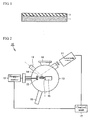
- FIG. 2 is a simplified configurational diagram of a PLD (pulsed laser deposition) film-producing system employable in the formation of aluminum nitride thin films.
- PLD pulse laser deposition
- the PLD film-producing system 10 is furnished with: a laser light source 11 that is capable of radiating a laser beam; a vacuum chamber 12; a stage 15 that is capable of carrying a sinter source material 14, which is the irradiation target; a stepper motor 13 that is capable of driving the stage 15; a holder 16 that is capable of retaining the base material 1; a control unit 17 that is able to carry out operational control of the stepper motor 13 and laser light source 11; a reflection high-energy electron diffraction (RHEED) 18; a gas-supply unit 19 that supplies gas to the vacuum chamber 12 interior; and a heater, installed in the holder 16, that is capable of heating the base material 1.
- the PLD film-producing system 10 includes various components other than the foregoing, but the illustration and description of such components is omitted for convenience of explanation.
- a sintered AIN ceramic containing between 0.001 wt. % and 10 wt. % additive atomic element of one or more type selected from Group-III atoms, Group-IV atoms and Group-V atoms is fabricated.
- the sintered AlN ceramic is fabricated, for example, by mixing together and press-forming 10 wt. % carbon powder, which is a Group-IV atomic element, and 90 wt. % of an AIN powder to prepare a compact, and sintering the compact 2 hours at 2000°C in a nitrogen atmosphere within a vacuum vessel (under a pressure of 10 -6 torr).
- carbon powder instead of the carbon powder, it is possible to utilize 10 wt. % of a silicon powder (Group-IV atomic element), or, at a combined total of 10 wt. %, a powder blend of silicon and carbon powders.
- the sintered AIN ceramic obtained as in the foregoing is set inside the vacuum chamber 12 represented in Fig. 2 . In particular, it is placed onto the stage 15 depicted in Fig. 2 .
- the base material 1, which is the film-deposition subject is set into a position that is on the front side of the holder 16 installed inside the vacuum chamber 12, and that opposes the foregoing sintered AIN ceramic.
- the front side of the base material 1 is preferably made flat. Preferably it is in a flat state in which, for example, a value expressing the average surface roughness per unit area as root mean square (RMS) is some 0.1 nm or less. Having the front side of the base material I be in a flat state can contribute to improving the flatness of the surface of the AIN thin film 2.
- RMS root mean square
- the laser beam that is emitted from the laser light source 11 hits onto the aforedescribed sintered AIN ceramic, being the sinter source material 14.
- a KrF excimer laser with a lasing wavelength of 248 nm, pulse-repetition frequency of 10 Hz, and per-pulse energy of 1 to 3 J/shot can, for example, be used as the laser.
- an ArF excimer laser whose lasing wavelength is 193 nm can also be employed.
- the vacuum chamber 12 interior is rendered a nitrogen atmosphere and put into a vacuum state of some 1 ⁇ 10 -3 torr to 1 ⁇ 10 -6 torr or less. Having the vacuum chamber 12 interior be a nitrogen atmosphere enables nitrogen to be supplied during formation of the AIN thin film 2. It will be appreciated that the nitrogen can be supplied to the vacuum chamber 12 interior by means of the gas-supply unit 19.
- a short-wavelength laser such as noted above is preferably used.
- the absorption coefficient will be large, such that in the vicinity of the sintered AIN ceramic front side, almost all of the laser light will thus be absorbed.
- the surface temperature of the sintered AIN ceramic rises abruptly as a result, making it possible to generate an ablation plasma (the plasma accompanying the explosive emission of particles from a solid) inside the vacuum chamber 12.
- the ablation particles contained within the plasma travel to the base material 1 while undergoing changes of state by recombining and by colliding and reacting with the ambient gas.
- the particles having arrived on the base material 1 then all disperse over the base material 1 and settle into stable sites to become a thin film.
- An AIN thin film 2 containing additive atomic elements of the sort listed earlier can thereby be grown onto the base material 1.
- the AIN thin film 2 When a foregoing AIN thin film 2 is to be grown, it is preferable that the AIN thin film 2, containing the aforesaid additive atomic elements, be formed while the base material 1 is heated. Heating the base material 1 to a temperature of some 800°C, for example, is preferable. To heat the base material 1. the above-noted heater installed in the vacuum chamber 12 may be employed, although the base material 1 can be heated by other methods, such as flowing a current into the base material 1.
- deposition thickness of the AIN thin film 2 can be monitored by means of oscillations from the reflection high-energy electron diffraction (RHEED) 18, mounted in the vacuum chamber 12.
- RHEED reflection high-energy electron diffraction
- the inventors in the present application actually fabricated by the aforedescribed technique AIN thin films 2 of approximately 5 nm thickness, containing 10 wt. % carbon and silicon, onto GaN substrates and onto Al 2 O 3 substrates of 1 inch (approx. 2.5 cm) diameter, and measured the surface roughness; the results will be explained using the table presented below.
- AFM atomic force microscope
- the comparative examples are instances in which an AIN thin film 2 of approximately 5 nm thickness was grown onto a GaN substrate and onto an Al 2 O 3 substrate, without adding atoms such as carbon and silicon;
- Comparative embodiment 1 is instances in which an AlN thin film 2 of approximately 5 nm thickness, containing 10 wt. % carbon, with the remainder being AIN and unavoidable impurities, was grown onto a GaN substrate and onto an Al 2 O 3 substrate;
- comparative embodiment 2 is instances in which an AIN thin film 2 of approximately 5 nm thickness, containing 10 wt.
- Embodiment 3 is instances in which an AIN thin film 2 of approximately 5 nm thickness, containing carbon and silicon at a combined total of 10 wt. %, with the remainder being AIN and unavoidable impurities, was grown onto a GaN substrate and onto an Al 2 O 3 substrate.
- Embodiments 3 As indicated in the table, it is evident that the degree of flatness in Embodiments 3 was markedly better than that in the comparative examples. Accordingly, it will be understood that deliberately adding atoms that are not unavoidable impurities allows the flatness of an AIN thin film 2 to be improved.
- FIGS. 3A and 3B are schematic diagrams for illustrating the operating principle of tunneling magnetoresistive devices
- Fig. 4 is a sectional diagram representing a structural example of a tunneling magnetoresistive device making application of an AIN thin film 2 in present Embodying Mode 1.
- the AIN thin films 2 described above should be applicable in functional devices like tunneling magnetoresistive devices and giant magnetoresistive devices, employing magnetoresistance; in light-emitting devices like light-emitting diodes and laser diodes; and in rectifiers and various electronic devices such as transistors of all kinds, including bipolar transistors, field-effect transistors (FETs), spin-FETs, and high electron mobility transistors (HEMTs).
- functional devices like tunneling magnetoresistive devices and giant magnetoresistive devices, employing magnetoresistance
- in light-emitting devices like light-emitting diodes and laser diodes
- rectifiers and various electronic devices such as transistors of all kinds, including bipolar transistors, field-effect transistors (FETs), spin-FETs, and high electron mobility transistors (HEMTs).
- FETs field-effect transistors
- HEMTs high electron mobility transistors
- an AIN thin film 2 of the present invention an implementation in which an AIN thin film 2 of the present invention is applied in a tunneling magnetoresistive device will be described.
- first and second ferromagnetic electrode layers 30 and 40 are formed sandwiching a tunnel barrier layer 20 between them.
- One of the first and second ferromagnetic electrode layers 30 and 40 is a fixed layer, while the other is a recording layer.
- the tunneling magnetoresistive device is formed onto a substrate 8.
- a semiconductor substrate such as a GaN substrate can, for example, be used as the substrate 8.
- a first ferromagnetic electrode layer 3, an AIN thin film 2 as a tunnel barrier layer, and a second ferromagnetic electrode layer 4 are formed in that order onto substrate 8.
- GaTMAs TM-magnetic transition-metal ion
- GaTMN GaTMN
- the AIN thin film 2 can be formed by a method described earlier, while the first and second ferromagnetic electrode layers 3 and 4 can be formed, for example, by a PLD process, or by molecular beam epitaxy (MBE) or sputtering.
- the layers are patterned into predetermined respective geometries. Further, after formation of the first ferromagnetic electrode layer 3, a conducting layer (electrode) 5 is formed onto the first ferromagnetic electrode layer 3.
- the conducting layer 5 is formed in a location where it will not overlap with the AlN thin film 2.
- the conducting layer 5 can be constituted by a metal material such as Cu, and is formable for example by creating a layer of metal material by a technique such as CVD or sputtering, and then patterning the metal-material layer into a predetermined geometry.
- an insulating layer 7 of silicon oxide or the like is formed, by CVD or a like technique, so as to cover the stacked-layer structure.
- the insulating layer 7 is subjected to a chemical mechanical polishing (CMP) operation, for example, to expose the surface of the second ferromagnetic electrode layer 4.
- CMP chemical mechanical polishing
- a conducting layer (electrode) is formed onto the second ferromagnetic electrode layer 4.
- This conducting layer also is formed in a location where it will not overlap with the AIN thin film 2.
- This conducting layer too can be constituted by a metal material such as Cu, and is formable for example by creating a layer of metal material by a technique such as CVD or sputtering, and then patterning the metal-material layer into a predetermined geometry.
- a tunneling magnetoresistive device in present Embodying Mode 2 is furnished with, as the tunnel barrier layer, an AIN thin film 2 that, as described above, is of excellent flatness and lattice matching and is of superior insulating properties, thus making possible the realization of a high on/off ratio while reducing leakage current.
Landscapes
- Chemical & Material Sciences (AREA)
- Engineering & Computer Science (AREA)
- Materials Engineering (AREA)
- Metallurgy (AREA)
- Organic Chemistry (AREA)
- Chemical Kinetics & Catalysis (AREA)
- Mechanical Engineering (AREA)
- Crystallography & Structural Chemistry (AREA)
- Health & Medical Sciences (AREA)
- Toxicology (AREA)
- Inorganic Chemistry (AREA)
- General Physics & Mathematics (AREA)
- Manufacturing & Machinery (AREA)
- Computer Hardware Design (AREA)
- Microelectronics & Electronic Packaging (AREA)
- Power Engineering (AREA)
- Condensed Matter Physics & Semiconductors (AREA)
- Physics & Mathematics (AREA)
- Physical Vapour Deposition (AREA)
- Hall/Mr Elements (AREA)
- Formation Of Insulating Films (AREA)
Claims (5)
- Film mince en nitrure d'aluminium, caractérisé en ce qu'il contient 10 % en poids d'élément atomique additif d'un mélange de carbone et de silicium, dans lequel le film mince en nitrure d'aluminium est disposé sur un matériau de base ayant une rugosité de surface inférieure ou égale à 0,1 nm.
- Procédé de fabrication d'un film mince en nitrure d'aluminium, comprenant :une étape consistant à disposer dans une chambre sous vide une céramique de nitrure d'aluminium fritté contenant 10 % en poids d'élément atomique additif d'un mélange de carbone et de silicium ;une étape consistant à disposer dans la chambre sous vide un matériau de base ayant une rugosité de surface inférieure ou égale à 0,1 nm ; etune étape consistant à irradier la céramique en nitrure d'aluminium fritté avec un laser pour évoluer vers un plasma, et utiliser le plasma pour former sur le matériau de base un film mince en nitrure d'aluminium contenant ledit élément atomique additif.
- Procédé de fabrication d'un film mince en nitrure d'aluminium selon la revendication 2, dans lequel la céramique en nitrure d'aluminium fritté contenant ledit élément atomique additif est fabriquée par frittage, en utilisant une atmosphère d'azote dans un récipient sous vide, un compact formé en mélangeant ensemble 10 % en poids d'une poudre dudit élément atomique additif et une poudre de nitrure d'aluminium.
- Procédé de fabrication d'un film mince en nitrure d'aluminium selon la revendication 2 ou 3, dans lequel le matériau de base est soit un substrat semiconducteur composé, soit un substrat isolant, et le film mince en nitrure d'aluminium contenant ledit élément atomique additif est formé pendant que le matériau de base est chauffé.
- Procédé de fabrication d'un film mince en nitrure d'aluminium selon l'une quelconque des revendications 2 à 4, dans lequel l'intérieur de la chambre sous vide est converti en une atmosphère d'azote ; et le plasma est un plasma d'ablation.
Applications Claiming Priority (3)
| Application Number | Priority Date | Filing Date | Title |
|---|---|---|---|
| JP2008046335 | 2008-02-27 | ||
| JP2009012038A JP2009228131A (ja) | 2008-02-27 | 2009-01-22 | 窒化アルミニウム薄膜およびその製造方法 |
| PCT/JP2009/052747 WO2009107525A1 (fr) | 2008-02-27 | 2009-02-18 | Film mince de nitrure d'aluminium et procédé de production du film mince de nitrure d'aluminium |
Publications (3)
| Publication Number | Publication Date |
|---|---|
| EP2246458A1 EP2246458A1 (fr) | 2010-11-03 |
| EP2246458A4 EP2246458A4 (fr) | 2012-03-07 |
| EP2246458B1 true EP2246458B1 (fr) | 2013-10-09 |
Family
ID=41015925
Family Applications (1)
| Application Number | Title | Priority Date | Filing Date |
|---|---|---|---|
| EP09714366.3A Not-in-force EP2246458B1 (fr) | 2008-02-27 | 2009-02-18 | Film mince de nitrure d'aluminium et procédé de production du film mince de nitrure d'aluminium |
Country Status (7)
| Country | Link |
|---|---|
| US (1) | US8367577B2 (fr) |
| EP (1) | EP2246458B1 (fr) |
| JP (1) | JP2009228131A (fr) |
| KR (1) | KR20100116109A (fr) |
| CN (1) | CN101970708B (fr) |
| CA (1) | CA2688453A1 (fr) |
| WO (1) | WO2009107525A1 (fr) |
Families Citing this family (6)
| Publication number | Priority date | Publication date | Assignee | Title |
|---|---|---|---|---|
| CN102299218B (zh) * | 2011-08-24 | 2015-04-01 | 上海蓝光科技有限公司 | 发光二极管及其制作方法 |
| KR102317822B1 (ko) * | 2012-07-02 | 2021-10-25 | 어플라이드 머티어리얼스, 인코포레이티드 | 물리 기상 증착에 의한 알루미늄-질화물 버퍼 및 활성 층들 |
| CN106062238B (zh) * | 2014-03-03 | 2018-09-04 | 株式会社村田制作所 | 氮化铝压电薄膜及其制造方法、压电材、压电部件 |
| JP6565118B2 (ja) * | 2015-08-24 | 2019-08-28 | 株式会社村田製作所 | 窒化アルミニウム圧電薄膜及びその製造方法、並びに圧電材及び圧電部品及び窒化アルミニウム圧電薄膜の製造方法 |
| GB2600570B (en) * | 2017-07-07 | 2022-11-16 | Skyworks Solutions Inc | Substituted aluminum nitride for improved acoustic wave filters |
| JP2020059644A (ja) * | 2018-10-10 | 2020-04-16 | 東ソー株式会社 | 窒化ガリウム系焼結体及びその製造方法 |
Family Cites Families (10)
| Publication number | Priority date | Publication date | Assignee | Title |
|---|---|---|---|---|
| JPH04342493A (ja) * | 1991-05-20 | 1992-11-27 | Fujitsu Ltd | レーザアブレーション装置 |
| JPH05320882A (ja) * | 1992-05-20 | 1993-12-07 | Mitsubishi Kasei Corp | 蒸着薄膜の作製法 |
| US5668524A (en) * | 1994-02-09 | 1997-09-16 | Kyocera Corporation | Ceramic resistor and electrostatic chuck having an aluminum nitride crystal phase |
| US7682709B1 (en) * | 1995-10-30 | 2010-03-23 | North Carolina State University | Germanium doped n-type aluminum nitride epitaxial layers |
| FR2798738B1 (fr) * | 1999-09-16 | 2001-10-26 | Saint Gobain Vitrage | Substrat transparent muni d'un empilement de couches reflechissant la chaleur |
| WO2004005216A1 (fr) * | 2002-07-09 | 2004-01-15 | Kenichiro Miyahara | Substrat permettant de former une couche mince, substrat a couche mince, guide d'ondes optique, element luminescent et substrat destine a porter un element luminescent |
| CN100414716C (zh) * | 2002-12-25 | 2008-08-27 | 松下电器产业株式会社 | 磁性开关元件及使用该元件的磁性存储器 |
| AU2003296063A1 (en) * | 2002-12-25 | 2004-07-22 | Matsushita Electric Industrial Co., Ltd. | Magnetic switching device and magnetic memory |
| US7544963B2 (en) * | 2005-04-29 | 2009-06-09 | Cree, Inc. | Binary group III-nitride based high electron mobility transistors |
| WO2007133512A2 (fr) * | 2006-05-08 | 2007-11-22 | The Regents Of The University Of California | Procédés et matériaux permettant de faire croître des composés semi-conducteurs de nitrure iii contenant de l'aluminium |
-
2009
- 2009-01-22 JP JP2009012038A patent/JP2009228131A/ja active Pending
- 2009-02-18 CN CN200980000384.4A patent/CN101970708B/zh not_active Expired - Fee Related
- 2009-02-18 KR KR1020097021671A patent/KR20100116109A/ko not_active Application Discontinuation
- 2009-02-18 EP EP09714366.3A patent/EP2246458B1/fr not_active Not-in-force
- 2009-02-18 US US12/602,104 patent/US8367577B2/en not_active Expired - Fee Related
- 2009-02-18 CA CA002688453A patent/CA2688453A1/fr not_active Abandoned
- 2009-02-18 WO PCT/JP2009/052747 patent/WO2009107525A1/fr active Application Filing
Also Published As
| Publication number | Publication date |
|---|---|
| CN101970708B (zh) | 2014-04-16 |
| US8367577B2 (en) | 2013-02-05 |
| KR20100116109A (ko) | 2010-10-29 |
| EP2246458A4 (fr) | 2012-03-07 |
| WO2009107525A1 (fr) | 2009-09-03 |
| JP2009228131A (ja) | 2009-10-08 |
| US20100209622A1 (en) | 2010-08-19 |
| CN101970708A (zh) | 2011-02-09 |
| CA2688453A1 (fr) | 2009-09-03 |
| EP2246458A1 (fr) | 2010-11-03 |
Similar Documents
| Publication | Publication Date | Title |
|---|---|---|
| JP5363525B2 (ja) | ダイヤモンド半導体素子およびその製造方法 | |
| EP2246458B1 (fr) | Film mince de nitrure d'aluminium et procédé de production du film mince de nitrure d'aluminium | |
| EP0601692A1 (fr) | Dispositif électronique avec un super-réseau artificiel | |
| CN106460229B (zh) | 掺杂的稀土氮化物材料和包含其的器件 | |
| Vereecken et al. | Magnetotransport properties of bismuth films on p-GaAs | |
| KR20160147791A (ko) | 희토류 나이트라이드를 포함하는 자성체 및 장치 | |
| US8715414B2 (en) | Process for producing Si(1-v-w-x)CwAlxNv base material, process for producing epitaxial wafer, Si(1-v-w-x)CwAlxNv base material, and epitaxial wafer | |
| Levander et al. | Growth and transport properties of p-type GaNBi alloys | |
| Nishimura et al. | Controlled carrier generation at a polarity-discontinued perovskite heterointerface | |
| WO2009131064A1 (fr) | Procede de production de materiau de base si<sb>(1-v-w-x)</sb>c<sb>w</sb>al<sb>x</sb>n<sb>v</sb>, procede de production de tranche epitaxiale, materiau de base si<sb>(1-v-w-x)</sb>c<sb>w</sb>al<sb>x</sb>n<sb>v</sb> et tranche epitaxiale ainsi produits | |
| JP2007246374A (ja) | 強磁性酸化物半導体薄膜及びその製造方法並びにこれを用いたスピントンネル磁気抵抗素子 | |
| Funk et al. | Magnetic Characterization of a Mn Based Ferromagnet on SixGe (1-xy) Sny with High Sn Content | |
| US11217743B2 (en) | Rare earth nitride structures and devices and method for removing a passivating capping | |
| Seo et al. | Electronic and optical characteristics of multilayer nanocrystalline silicon/adsorbed oxygen superlattice | |
| Khan | NiO x Based Device Structures | |
| Suzuki | Pulsed laser deposition of filled skutterudite LaFe3CoSb12 thin films | |
| Satoh et al. | Process for producing Si (1-vwx) C w Al x N v base material, process for producing epitaxial wafer, Si (1-vwx) C w Al x N v base material, and epitaxial wafer | |
| Tamil Many | A novel technique for the synthesis of pure and doped zinc oxide nanostructures using thermal chemical vapor deposition method/Tamil Many K. Thandavan | |
| Thandavan | A Novel Technique for the Synthesis of Pure and Doped Zinc Oxide Nanostructures Using Thermal Chemical Vapor Deposition Method | |
| Koleva et al. | Characterization of vanadium doped ZnO films produced by pulsed laser deposition | |
| Warren | Influence of Embedded Metallic Nanocrystals on GaAs Thermoelectric Properties. |
Legal Events
| Date | Code | Title | Description |
|---|---|---|---|
| PUAI | Public reference made under article 153(3) epc to a published international application that has entered the european phase |
Free format text: ORIGINAL CODE: 0009012 |
|
| 17P | Request for examination filed |
Effective date: 20091125 |
|
| AK | Designated contracting states |
Kind code of ref document: A1 Designated state(s): AT BE BG CH CY CZ DE DK EE ES FI FR GB GR HR HU IE IS IT LI LT LU LV MC MK MT NL NO PL PT RO SE SI SK TR |
|
| AX | Request for extension of the european patent |
Extension state: AL BA RS |
|
| DAX | Request for extension of the european patent (deleted) | ||
| A4 | Supplementary search report drawn up and despatched |
Effective date: 20120208 |
|
| RIC1 | Information provided on ipc code assigned before grant |
Ipc: C30B 29/38 20060101ALI20120203BHEP Ipc: C23C 14/28 20060101ALI20120203BHEP Ipc: C30B 29/40 20060101ALI20120203BHEP Ipc: C30B 23/02 20060101ALI20120203BHEP Ipc: C23C 14/06 20060101AFI20120203BHEP |
|
| RIC1 | Information provided on ipc code assigned before grant |
Ipc: C30B 29/38 20060101ALI20130308BHEP Ipc: C30B 29/40 20060101ALI20130308BHEP Ipc: C23C 14/28 20060101ALI20130308BHEP Ipc: C30B 23/02 20060101ALI20130308BHEP Ipc: C23C 14/06 20060101AFI20130308BHEP |
|
| GRAP | Despatch of communication of intention to grant a patent |
Free format text: ORIGINAL CODE: EPIDOSNIGR1 |
|
| INTG | Intention to grant announced |
Effective date: 20130423 |
|
| GRAS | Grant fee paid |
Free format text: ORIGINAL CODE: EPIDOSNIGR3 |
|
| GRAA | (expected) grant |
Free format text: ORIGINAL CODE: 0009210 |
|
| AK | Designated contracting states |
Kind code of ref document: B1 Designated state(s): AT BE BG CH CY CZ DE DK EE ES FI FR GB GR HR HU IE IS IT LI LT LU LV MC MK MT NL NO PL PT RO SE SI SK TR |
|
| REG | Reference to a national code |
Ref country code: GB Ref legal event code: FG4D |
|
| REG | Reference to a national code |
Ref country code: AT Ref legal event code: REF Ref document number: 635608 Country of ref document: AT Kind code of ref document: T Effective date: 20131015 Ref country code: CH Ref legal event code: EP |
|
| REG | Reference to a national code |
Ref country code: IE Ref legal event code: FG4D |
|
| REG | Reference to a national code |
Ref country code: DE Ref legal event code: R096 Ref document number: 602009019326 Country of ref document: DE Effective date: 20131205 |
|
| REG | Reference to a national code |
Ref country code: AT Ref legal event code: MK05 Ref document number: 635608 Country of ref document: AT Kind code of ref document: T Effective date: 20131009 |
|
| REG | Reference to a national code |
Ref country code: NL Ref legal event code: VDEP Effective date: 20131009 |
|
| PG25 | Lapsed in a contracting state [announced via postgrant information from national office to epo] |
Ref country code: SI Free format text: LAPSE BECAUSE OF FAILURE TO SUBMIT A TRANSLATION OF THE DESCRIPTION OR TO PAY THE FEE WITHIN THE PRESCRIBED TIME-LIMIT Effective date: 20131009 |
|
| REG | Reference to a national code |
Ref country code: LT Ref legal event code: MG4D |
|
| PG25 | Lapsed in a contracting state [announced via postgrant information from national office to epo] |
Ref country code: LT Free format text: LAPSE BECAUSE OF FAILURE TO SUBMIT A TRANSLATION OF THE DESCRIPTION OR TO PAY THE FEE WITHIN THE PRESCRIBED TIME-LIMIT Effective date: 20131009 Ref country code: NO Free format text: LAPSE BECAUSE OF FAILURE TO SUBMIT A TRANSLATION OF THE DESCRIPTION OR TO PAY THE FEE WITHIN THE PRESCRIBED TIME-LIMIT Effective date: 20140109 Ref country code: SE Free format text: LAPSE BECAUSE OF FAILURE TO SUBMIT A TRANSLATION OF THE DESCRIPTION OR TO PAY THE FEE WITHIN THE PRESCRIBED TIME-LIMIT Effective date: 20131009 Ref country code: IS Free format text: LAPSE BECAUSE OF FAILURE TO SUBMIT A TRANSLATION OF THE DESCRIPTION OR TO PAY THE FEE WITHIN THE PRESCRIBED TIME-LIMIT Effective date: 20140209 Ref country code: HR Free format text: LAPSE BECAUSE OF FAILURE TO SUBMIT A TRANSLATION OF THE DESCRIPTION OR TO PAY THE FEE WITHIN THE PRESCRIBED TIME-LIMIT Effective date: 20131009 Ref country code: FI Free format text: LAPSE BECAUSE OF FAILURE TO SUBMIT A TRANSLATION OF THE DESCRIPTION OR TO PAY THE FEE WITHIN THE PRESCRIBED TIME-LIMIT Effective date: 20131009 Ref country code: NL Free format text: LAPSE BECAUSE OF FAILURE TO SUBMIT A TRANSLATION OF THE DESCRIPTION OR TO PAY THE FEE WITHIN THE PRESCRIBED TIME-LIMIT Effective date: 20131009 Ref country code: BE Free format text: LAPSE BECAUSE OF FAILURE TO SUBMIT A TRANSLATION OF THE DESCRIPTION OR TO PAY THE FEE WITHIN THE PRESCRIBED TIME-LIMIT Effective date: 20131009 |
|
| PG25 | Lapsed in a contracting state [announced via postgrant information from national office to epo] |
Ref country code: LV Free format text: LAPSE BECAUSE OF FAILURE TO SUBMIT A TRANSLATION OF THE DESCRIPTION OR TO PAY THE FEE WITHIN THE PRESCRIBED TIME-LIMIT Effective date: 20131009 Ref country code: CY Free format text: LAPSE BECAUSE OF FAILURE TO SUBMIT A TRANSLATION OF THE DESCRIPTION OR TO PAY THE FEE WITHIN THE PRESCRIBED TIME-LIMIT Effective date: 20131009 Ref country code: AT Free format text: LAPSE BECAUSE OF FAILURE TO SUBMIT A TRANSLATION OF THE DESCRIPTION OR TO PAY THE FEE WITHIN THE PRESCRIBED TIME-LIMIT Effective date: 20131009 Ref country code: PL Free format text: LAPSE BECAUSE OF FAILURE TO SUBMIT A TRANSLATION OF THE DESCRIPTION OR TO PAY THE FEE WITHIN THE PRESCRIBED TIME-LIMIT Effective date: 20131009 Ref country code: ES Free format text: LAPSE BECAUSE OF FAILURE TO SUBMIT A TRANSLATION OF THE DESCRIPTION OR TO PAY THE FEE WITHIN THE PRESCRIBED TIME-LIMIT Effective date: 20131009 |
|
| PG25 | Lapsed in a contracting state [announced via postgrant information from national office to epo] |
Ref country code: PT Free format text: LAPSE BECAUSE OF FAILURE TO SUBMIT A TRANSLATION OF THE DESCRIPTION OR TO PAY THE FEE WITHIN THE PRESCRIBED TIME-LIMIT Effective date: 20140210 |
|
| REG | Reference to a national code |
Ref country code: DE Ref legal event code: R097 Ref document number: 602009019326 Country of ref document: DE |
|
| PG25 | Lapsed in a contracting state [announced via postgrant information from national office to epo] |
Ref country code: EE Free format text: LAPSE BECAUSE OF FAILURE TO SUBMIT A TRANSLATION OF THE DESCRIPTION OR TO PAY THE FEE WITHIN THE PRESCRIBED TIME-LIMIT Effective date: 20131009 |
|
| PLBE | No opposition filed within time limit |
Free format text: ORIGINAL CODE: 0009261 |
|
| STAA | Information on the status of an ep patent application or granted ep patent |
Free format text: STATUS: NO OPPOSITION FILED WITHIN TIME LIMIT |
|
| PG25 | Lapsed in a contracting state [announced via postgrant information from national office to epo] |
Ref country code: SK Free format text: LAPSE BECAUSE OF FAILURE TO SUBMIT A TRANSLATION OF THE DESCRIPTION OR TO PAY THE FEE WITHIN THE PRESCRIBED TIME-LIMIT Effective date: 20131009 Ref country code: CZ Free format text: LAPSE BECAUSE OF FAILURE TO SUBMIT A TRANSLATION OF THE DESCRIPTION OR TO PAY THE FEE WITHIN THE PRESCRIBED TIME-LIMIT Effective date: 20131009 Ref country code: IT Free format text: LAPSE BECAUSE OF FAILURE TO SUBMIT A TRANSLATION OF THE DESCRIPTION OR TO PAY THE FEE WITHIN THE PRESCRIBED TIME-LIMIT Effective date: 20131009 Ref country code: RO Free format text: LAPSE BECAUSE OF FAILURE TO SUBMIT A TRANSLATION OF THE DESCRIPTION OR TO PAY THE FEE WITHIN THE PRESCRIBED TIME-LIMIT Effective date: 20131009 |
|
| 26N | No opposition filed |
Effective date: 20140710 |
|
| PG25 | Lapsed in a contracting state [announced via postgrant information from national office to epo] |
Ref country code: MC Free format text: LAPSE BECAUSE OF FAILURE TO SUBMIT A TRANSLATION OF THE DESCRIPTION OR TO PAY THE FEE WITHIN THE PRESCRIBED TIME-LIMIT Effective date: 20131009 Ref country code: DK Free format text: LAPSE BECAUSE OF FAILURE TO SUBMIT A TRANSLATION OF THE DESCRIPTION OR TO PAY THE FEE WITHIN THE PRESCRIBED TIME-LIMIT Effective date: 20131009 Ref country code: LU Free format text: LAPSE BECAUSE OF FAILURE TO SUBMIT A TRANSLATION OF THE DESCRIPTION OR TO PAY THE FEE WITHIN THE PRESCRIBED TIME-LIMIT Effective date: 20140218 |
|
| REG | Reference to a national code |
Ref country code: CH Ref legal event code: PL |
|
| REG | Reference to a national code |
Ref country code: DE Ref legal event code: R097 Ref document number: 602009019326 Country of ref document: DE Effective date: 20140710 |
|
| PG25 | Lapsed in a contracting state [announced via postgrant information from national office to epo] |
Ref country code: LI Free format text: LAPSE BECAUSE OF NON-PAYMENT OF DUE FEES Effective date: 20140228 Ref country code: CH Free format text: LAPSE BECAUSE OF NON-PAYMENT OF DUE FEES Effective date: 20140228 |
|
| REG | Reference to a national code |
Ref country code: IE Ref legal event code: MM4A |
|
| PG25 | Lapsed in a contracting state [announced via postgrant information from national office to epo] |
Ref country code: IE Free format text: LAPSE BECAUSE OF NON-PAYMENT OF DUE FEES Effective date: 20140218 |
|
| REG | Reference to a national code |
Ref country code: FR Ref legal event code: PLFP Year of fee payment: 8 |
|
| PG25 | Lapsed in a contracting state [announced via postgrant information from national office to epo] |
Ref country code: MT Free format text: LAPSE BECAUSE OF FAILURE TO SUBMIT A TRANSLATION OF THE DESCRIPTION OR TO PAY THE FEE WITHIN THE PRESCRIBED TIME-LIMIT Effective date: 20131009 |
|
| PG25 | Lapsed in a contracting state [announced via postgrant information from national office to epo] |
Ref country code: BG Free format text: LAPSE BECAUSE OF FAILURE TO SUBMIT A TRANSLATION OF THE DESCRIPTION OR TO PAY THE FEE WITHIN THE PRESCRIBED TIME-LIMIT Effective date: 20131009 |
|
| PG25 | Lapsed in a contracting state [announced via postgrant information from national office to epo] |
Ref country code: GR Free format text: LAPSE BECAUSE OF FAILURE TO SUBMIT A TRANSLATION OF THE DESCRIPTION OR TO PAY THE FEE WITHIN THE PRESCRIBED TIME-LIMIT Effective date: 20140110 |
|
| PG25 | Lapsed in a contracting state [announced via postgrant information from national office to epo] |
Ref country code: TR Free format text: LAPSE BECAUSE OF FAILURE TO SUBMIT A TRANSLATION OF THE DESCRIPTION OR TO PAY THE FEE WITHIN THE PRESCRIBED TIME-LIMIT Effective date: 20131009 Ref country code: HU Free format text: LAPSE BECAUSE OF FAILURE TO SUBMIT A TRANSLATION OF THE DESCRIPTION OR TO PAY THE FEE WITHIN THE PRESCRIBED TIME-LIMIT; INVALID AB INITIO Effective date: 20090218 |
|
| REG | Reference to a national code |
Ref country code: FR Ref legal event code: PLFP Year of fee payment: 9 |
|
| PGFP | Annual fee paid to national office [announced via postgrant information from national office to epo] |
Ref country code: FR Payment date: 20170112 Year of fee payment: 9 |
|
| PGFP | Annual fee paid to national office [announced via postgrant information from national office to epo] |
Ref country code: GB Payment date: 20170215 Year of fee payment: 9 |
|
| PG25 | Lapsed in a contracting state [announced via postgrant information from national office to epo] |
Ref country code: MK Free format text: LAPSE BECAUSE OF FAILURE TO SUBMIT A TRANSLATION OF THE DESCRIPTION OR TO PAY THE FEE WITHIN THE PRESCRIBED TIME-LIMIT Effective date: 20131009 |
|
| GBPC | Gb: european patent ceased through non-payment of renewal fee |
Effective date: 20180218 |
|
| REG | Reference to a national code |
Ref country code: FR Ref legal event code: ST Effective date: 20181031 |
|
| PG25 | Lapsed in a contracting state [announced via postgrant information from national office to epo] |
Ref country code: FR Free format text: LAPSE BECAUSE OF NON-PAYMENT OF DUE FEES Effective date: 20180228 Ref country code: GB Free format text: LAPSE BECAUSE OF NON-PAYMENT OF DUE FEES Effective date: 20180218 |
|
| PGFP | Annual fee paid to national office [announced via postgrant information from national office to epo] |
Ref country code: DE Payment date: 20211230 Year of fee payment: 14 |
|
| REG | Reference to a national code |
Ref country code: DE Ref legal event code: R119 Ref document number: 602009019326 Country of ref document: DE |
|
| PG25 | Lapsed in a contracting state [announced via postgrant information from national office to epo] |
Ref country code: DE Free format text: LAPSE BECAUSE OF NON-PAYMENT OF DUE FEES Effective date: 20230901 |