EP2244331A1 - Planarer Wellenleiter - Google Patents
Planarer Wellenleiter Download PDFInfo
- Publication number
- EP2244331A1 EP2244331A1 EP09290299A EP09290299A EP2244331A1 EP 2244331 A1 EP2244331 A1 EP 2244331A1 EP 09290299 A EP09290299 A EP 09290299A EP 09290299 A EP09290299 A EP 09290299A EP 2244331 A1 EP2244331 A1 EP 2244331A1
- Authority
- EP
- European Patent Office
- Prior art keywords
- central line
- carrier
- planar waveguide
- dielectric layer
- flange
- Prior art date
- Legal status (The legal status is an assumption and is not a legal conclusion. Google has not performed a legal analysis and makes no representation as to the accuracy of the status listed.)
- Withdrawn
Links
- 230000005540 biological transmission Effects 0.000 claims abstract description 6
- 229910052751 metal Inorganic materials 0.000 claims description 27
- 239000002184 metal Substances 0.000 claims description 27
- 239000000758 substrate Substances 0.000 claims description 6
- 238000000034 method Methods 0.000 claims description 3
- 238000005516 engineering process Methods 0.000 description 10
- 230000005672 electromagnetic field Effects 0.000 description 3
- VYPSYNLAJGMNEJ-UHFFFAOYSA-N Silicium dioxide Chemical compound O=[Si]=O VYPSYNLAJGMNEJ-UHFFFAOYSA-N 0.000 description 2
- 238000010586 diagram Methods 0.000 description 2
- 230000000694 effects Effects 0.000 description 2
- 230000005684 electric field Effects 0.000 description 2
- JBRZTFJDHDCESZ-UHFFFAOYSA-N AsGa Chemical compound [As]#[Ga] JBRZTFJDHDCESZ-UHFFFAOYSA-N 0.000 description 1
- 229910001218 Gallium arsenide Inorganic materials 0.000 description 1
- 239000004642 Polyimide Substances 0.000 description 1
- 235000001537 Ribes X gardonianum Nutrition 0.000 description 1
- 235000001535 Ribes X utile Nutrition 0.000 description 1
- 235000016919 Ribes petraeum Nutrition 0.000 description 1
- 244000281247 Ribes rubrum Species 0.000 description 1
- 235000002355 Ribes spicatum Nutrition 0.000 description 1
- 229910052581 Si3N4 Inorganic materials 0.000 description 1
- 229910004541 SiN Inorganic materials 0.000 description 1
- 239000000919 ceramic Substances 0.000 description 1
- 229910052681 coesite Inorganic materials 0.000 description 1
- 229910052906 cristobalite Inorganic materials 0.000 description 1
- 229920001721 polyimide Polymers 0.000 description 1
- 229910052710 silicon Inorganic materials 0.000 description 1
- 239000010703 silicon Substances 0.000 description 1
- 239000000377 silicon dioxide Substances 0.000 description 1
- 235000012239 silicon dioxide Nutrition 0.000 description 1
- 229910052682 stishovite Inorganic materials 0.000 description 1
- 229910052905 tridymite Inorganic materials 0.000 description 1
Images


Classifications
-
- H—ELECTRICITY
- H01—ELECTRIC ELEMENTS
- H01P—WAVEGUIDES; RESONATORS, LINES, OR OTHER DEVICES OF THE WAVEGUIDE TYPE
- H01P3/00—Waveguides; Transmission lines of the waveguide type
- H01P3/003—Coplanar lines
Definitions
- the subject matter relates to a planar waveguide, an integrated circuit comprising a planar waveguide, a use of a planar waveguide and a method for assembling a planar waveguide.
- Coplanar transmission lines are widely used in the microwave domain as well as in integrated circuits.
- MMIC microwave-integrated circuits
- planar transmission lines it is necessary to reduce losses at high frequency and to achieve low impedance.
- Figure 1 illustrates a common structure of a coplanar waveguide.
- a coplanar waveguide may be comprised of a carrier 2, with a substrate 3, a dielectric layer 4 and a top metal layer 8.
- the coplanar waveguide according to prior art can be made with a top metal layer 8 having a certain pattern, i.e. a ground plane, top metal layers 8a and 8b, and a signal track 10 (also being a metal layer) with a defined space (gap) between the ground planes and the signal track.
- the metal layer 8 is then arranged to make a coplanar waveguide.
- Two ground planes 8a, 8b can be arranged on the surface of the carrier 2.
- the central line 10 may have a width W, and the distance between the central line 10 and the ground plane 8b can be a gap G.
- the ground planes 8 and the central line 10 are arranged coplanar on the surface of the carrier 2, in particular on the surface of the dielectric layer 4.
- the electromagnetic field of signals on the central line 10 propagates around the central line 10.
- the loss factor as well as the characteristic impedance strongly depend on the width W and the gap G, and need to be reduced. However, it has been found that in the shown coplanar structure the loss factor at high frequency is high. Further, the impedance characteristic of the described structure can hardly be below 20 Ohms, as in this case the gap G needs to be very small. However, some technology constraints require the gap G to be larger than 10 ⁇ m, for example larger than 50 ⁇ m, for example larger than 100 ⁇ m.
- the constraint on the gap G as well as the constraint on the width W which may be due to area constraints on the integrated circuit, provide for increased losses at high frequencies and higher impedance characteristics than desired.
- embodiments of the invention comprise a planar waveguide comprising a carrier, at least two ground planes arranged on one surface of the carrier, at least one central line on which a transmission signal propagates and which is arranged on the one surface of the carrier in between the ground planes, wherein the central line extends from the surface of the carrier into the carrier.
- the loss factor can be improved in particular at high frequencies, in particular at frequencies above 10 GHz, in particular at frequencies between 10 and 100 GHz.
- the impedance characteristic can be improved within a range of 1 GHz to 100 GHz.
- the impedance can be reduced by at least 5 Ohms, preferably at least 10 Ohms by extending the central line into the carrier and possibly reducing thus the effective distance between the central line and the ground plane.
- the central line extends further into the carrier than the ground planes.
- the central line is arranged in between the ground planes with a gap to at least one ground plane.
- the gap to the ground plane on the surface may be imposed due to technology constraints. For example, some technologies require a space between the central line and the ground plane of at least 10 ⁇ m. By providing the gap between the ground plane and the central line, these technology constraints can be met.
- the carrier comprises at least one substrate and at least one top metal layer, wherein the central line extends at least through the top metal layer.
- the carrier may be possible to deposit first a first dielectric layer on top of a carrier. Then it may be possible to deposit a first metal layer with the appropriate shape onto the dielectric layer.
- a second dielectric layer may be deposited on top of the first metal layer. Via holes may be created in that second dielectric layer in order to connect the first metal layer to a second, topmost top metal layer 10, to make a final signal line.
- Ground planes may also be deposited as topmost top metal layers.
- the dielectric layer(s) may be composed of SiO2, Si3N4, SiN, Polyimide, or the like.
- the central line may have an increased width within the carrier. It has been found that the effective distance between at least one ground plane, preferably both ground planes, and the central line can be reduced by increasing the width of the central line at the portion which extends into the carrier.
- the width of the portion of the central line being arranged on the surface of the carrier is 30 ⁇ m
- the width of the central line arranged below the surface of the carrier, i.e. within the carrier can be 60 ⁇ m.
- the gap G between the central line and the ground planes can be reduced at least by a portion of the central line being arranged underneath the surface of the carrier.
- the effective width can be smaller than the width of the central line on the surface of the carrier.
- a bar may extend from the central line into the carrier, thus extending at least into the top metal layer and connecting a lower portion of the central line with a portion of the central line being arranged on the surface of the substrate.
- the bar is arranged substantially centered on the central line such that the central line is T-shaped.
- embodiments provide for a flange extending from the bar and being arranged within the carrier.
- the flange may be parallel to the portion of the central line being arranged on the surface of the carrier.
- the width of the flange may be bigger than the width of the central line.
- the flange can be straight.
- the flange may run in parallel to the surface of the carrier and thus in parallel to the central line.
- the flange may be v-shaped.
- the flange may be stepped. It may be possible that the flange may be v-shaped, being opened into the direction of the carrier. It may for example be possible to have a stepped flange, whereby each step of the flange may constitute one layer of the central line. For example, in multi-layer technology, where one central line and several ground planes are arranged on top of each other, multi-layered, each step of the flange may constitute one central line within the respective layer.
- an integrated circuit comprising a waveguide as described above.
- An integrated circuit having a planar waveguide as described above may propagate microwave signals at reduced losses.
- a wave guide as described above is provided in microwave signal propagation.
- Another aspect is a method for assembling a waveguide of claim 1 comprising arranging a first dielectric layer onto a carrier, arranging a first metal layer onto the first dielectric layer, arranging a second dielectric layer on the first metal layer, arranging a top metal layer on the second dielectric layer, wherein the top metal layer is comprised of at least one central line and at least one ground line, and wherein the at least one central line is electrically connected to at least the first metal layers by via holes through the second dielectric layer.
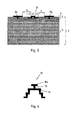
- FIG. 2 illustrates a coplanar waveguide structure according to embodiments.
- the illustration in Figure 2 is schematically and shows the coplanar structure in a side view.
- a carrier 2 with a substrate 3, a first dielectric layer 4 and a second dielectric layer 6 are is used for carrying on its surface a top metal layer comprised of at least two ground planes 8a, 8b and a central line 10.
- the central line 10 which extends, parallel to the ground planes 8a, 8b, on the surface of carrier 2.
- a gap G between the central line 10 and the ground planes 8a, 8b is provided on the central line 10.
- a high frequency signal may propagate.
- central line 10 comprises a bar 12, being arranged centrally to the central line 10.
- the bar 12 ends in a flange 14, which flange 14 may be arranged in between the first dielectric layer 4 and the second dielectric layer 6 and may constitute a metal layer.
- bar 12 extends by via holes through the second dielectric layer 6 to connect to the flange 14.
- the flange 14 is arranged beneath the surface of carrier 2, more particularly in between dielectric layer 6 and dielectric layer 4.
- the flange 14 has a width which is bigger than the width W of the portion of the central line 10 being arranged on the surface of the carrier 2.
- the gap G between the central line 10 and the ground planes 8a, 8b can be reduced to obtain a delta parameter ⁇ , which can be used to optimize the loss factor and the impedance.
- the loss factor as well as the impedance can be reduced for high frequencies.
- the central line extends further into the carrier than the ground planes.
- Figure 3 illustrates another possible structure of a coplanar waveguide according to embodiments.
- the central line 10 into the dielectric layer 6
- FIG. 4 illustrates a central line 10 in more detail according to an embodiment.
- a top portion 10a of the central line 10 can be straight. This top portion 10a can be arranged on the surface of the carrier 2. Centrally to the top portion 10a, there can be arranged a bar 12. Top portion 10a and bar 12 constitute a T-shape. Bar 12 may extend into flange 14.
- flange 14 can be v-shaped, with the opening in the direction of carrier 2.
- flange 14 can be stepped, where several steps may be constituted within flange 14. The effective width of flange 14 may be bigger than the width of the top portion 10a of the central line 10.
- Figure 5a illustrates the loss factor of a planar waveguide according to the above described embodiments compared to conventional coplanar waveguides.
- the abscissa indicates the frequency, whereas the ordinate indicates the loss factor in dB/mm.
- Slope 16 illustrates the loss factor of a conventional coplanar wave guide.
- the loss factor increases to about -0,8 dB/mm at 100 GHz.
- the slope 18 shows the loss factor of the coplanar waveguides according to embodiments.
- the loss factor is only -0,4 dB/mm, compared to - 0,8 dB/mm for a conventional coplanar waveguide.
- Figure 5b illustrates the impedance Re (Zc) of a coplanar waveguide according to embodiments compared to a conventional coplanar waveguide.
- the abscissa again illustrates the frequency in gigahertz, and the ordinate illustrates the impedance in Ohm.
- the impedance of a conventional coplanar waveguide is around 70 and 80 Ohms between 1 and 100 GHz.
- the impedance of a coplanar waveguide according to embodiments lies between 64 and 62 Ohm, which is an improvement of more than 10 Ohm.
- the reduction of loss factor and impedance is obtained due to the confinement of the electromagnetic fields in the low permittivity region and because the currant curving effects are reduced in the waveguide according to embodiments.
- the resistance of the signal line (central line 10) can be reduced.
- the area of the metal cross section can be larger than in a conventional design.
- the characteristic impedance can be lowered because the electric field between the signal line and the ground planes may be bigger, due to a bigger gap G. This electric field may increase the capacitance to ground C and therefore reduce the impedance of the signal line.
Landscapes
- Waveguides (AREA)
Priority Applications (1)
| Application Number | Priority Date | Filing Date | Title |
|---|---|---|---|
| EP09290299A EP2244331A1 (de) | 2009-04-22 | 2009-04-22 | Planarer Wellenleiter |
Applications Claiming Priority (1)
| Application Number | Priority Date | Filing Date | Title |
|---|---|---|---|
| EP09290299A EP2244331A1 (de) | 2009-04-22 | 2009-04-22 | Planarer Wellenleiter |
Publications (1)
| Publication Number | Publication Date |
|---|---|
| EP2244331A1 true EP2244331A1 (de) | 2010-10-27 |
Family
ID=40957731
Family Applications (1)
| Application Number | Title | Priority Date | Filing Date |
|---|---|---|---|
| EP09290299A Withdrawn EP2244331A1 (de) | 2009-04-22 | 2009-04-22 | Planarer Wellenleiter |
Country Status (1)
| Country | Link |
|---|---|
| EP (1) | EP2244331A1 (de) |
Cited By (1)
| Publication number | Priority date | Publication date | Assignee | Title |
|---|---|---|---|---|
| WO2023037852A1 (ja) * | 2021-09-07 | 2023-03-16 | 株式会社村田製作所 | 多層基板 |
Citations (1)
| Publication number | Priority date | Publication date | Assignee | Title |
|---|---|---|---|---|
| WO2009048207A1 (en) * | 2007-10-08 | 2009-04-16 | Samsung Electronics Co., Ltd. | Waveguide of multi-layer metal structure and manufacturing method thereof |
-
2009
- 2009-04-22 EP EP09290299A patent/EP2244331A1/de not_active Withdrawn
Patent Citations (1)
| Publication number | Priority date | Publication date | Assignee | Title |
|---|---|---|---|---|
| WO2009048207A1 (en) * | 2007-10-08 | 2009-04-16 | Samsung Electronics Co., Ltd. | Waveguide of multi-layer metal structure and manufacturing method thereof |
Non-Patent Citations (3)
| Title |
|---|
| BUDIMIR D ET AL: "LOW LOSS MULTILAYER COPLANAR WAVEGUIDE TRANSMISSION LINES ON SILICON SUBSTRATE FOR MMICS", PROCEEDINGS OF THE 26TH. EUROPEAN MICROWAVE CONFERENCE 1996. PRAGUE, SEPT. 9 - 13, 1996; [PROCEEDINGS OF THE EUROPEAN MICROWAVE CONFERENCE], SWANLEY, NEXUS MEDIA, GB, vol. CONF. 26, 9 September 1996 (1996-09-09), pages 697 - 700, XP000682626, ISBN: 978-1-899919-08-6 * |
| GILLICK M ET AL: "Ultra low impedance CPW transmission lines for multilayer MMICs", MICROWAVE SYMPOSIUM DIGEST, 1993., IEEE MTT-S INTERNATIONAL ATLANTA, GA, USA 14-18 JUNE 1993, NEW YORK, NY, USA,IEEE, US, 14 June 1993 (1993-06-14), pages 145 - 148, XP010068254, ISBN: 978-0-7803-1209-8 * |
| HONG-TEUK KIM ET AL: "A New Micromachined Overlay CPW Structure With Low Attenuation Over Wide Impedance Ranges and Its Application to Low-Pass Filters", IEEE TRANSACTIONS ON MICROWAVE THEORY AND TECHNIQUES, IEEE SERVICE CENTER, PISCATAWAY, NJ, US, vol. 49, no. 9, 1 September 2001 (2001-09-01), XP011038400, ISSN: 0018-9480 * |
Cited By (4)
| Publication number | Priority date | Publication date | Assignee | Title |
|---|---|---|---|---|
| WO2023037852A1 (ja) * | 2021-09-07 | 2023-03-16 | 株式会社村田製作所 | 多層基板 |
| JPWO2023037852A1 (de) * | 2021-09-07 | 2023-03-16 | ||
| JP7525071B2 (ja) | 2021-09-07 | 2024-07-30 | 株式会社村田製作所 | 多層基板 |
| US12439505B2 (en) | 2021-09-07 | 2025-10-07 | Murata Manufacturing Co., Ltd. | Multilayer substrate |
Similar Documents
| Publication | Publication Date | Title |
|---|---|---|
| KR100731544B1 (ko) | 다층배선 코플래너 웨이브가이드 | |
| US8471646B2 (en) | Wideband, differential signal balun for rejecting common mode electromagnetic fields | |
| CA2712949C (en) | A radio frequency circuit board topology | |
| JP4371065B2 (ja) | 伝送線路、通信装置及び配線形成方法 | |
| US6400234B1 (en) | Strip line feeding apparatus | |
| JP4958849B2 (ja) | 差動伝送線路 | |
| JP5725013B2 (ja) | 構造体、配線基板および配線基板の製造方法 | |
| US6441471B1 (en) | Wiring substrate for high frequency applications | |
| US6617943B1 (en) | Package substrate interconnect layout for providing bandpass/lowpass filtering | |
| AU2013279083B2 (en) | Balun | |
| JP4535995B2 (ja) | 多層プリント回路基板のビア構造、それを有する帯域阻止フィルタ | |
| CN111653853A (zh) | 一种无过孔的锯齿型带状线共模滤波电路 | |
| JP4722614B2 (ja) | 方向性結合器及び180°ハイブリッドカプラ | |
| US7688164B2 (en) | High frequency circuit board converting a transmission mode of high frequency signals | |
| EP2244331A1 (de) | Planarer Wellenleiter | |
| JP2018182422A (ja) | 基板集積導波管 | |
| JP2004064174A (ja) | 高周波用配線基板 | |
| JP2011109431A (ja) | 導波管−マイクロストリップ線路変換器および導波管−マイクロストリップ線路変換器の製造方法 | |
| CN100365864C (zh) | 改进的定向耦合器 | |
| WO2008108003A1 (en) | Compact filtering structure | |
| JP2018148550A (ja) | 高周波用差動信号伝送線路及びそれを備えた信号伝送システム | |
| KR100329910B1 (ko) | 분포 상수 선로의 결합방법 및 마이크로파 회로 | |
| JP6491080B2 (ja) | 多層配線基板 | |
| CN115799792B (zh) | 一种应用于Sub6G的微带双频防雷电路 | |
| EP1357632B1 (de) | Verfahren zur Unterdrückung von Störungen in mehrlagigen Mikrostreifenleitungen mit mehreren Leitern |
Legal Events
| Date | Code | Title | Description |
|---|---|---|---|
| PUAI | Public reference made under article 153(3) epc to a published international application that has entered the european phase |
Free format text: ORIGINAL CODE: 0009012 |
|
| AK | Designated contracting states |
Kind code of ref document: A1 Designated state(s): AT BE BG CH CY CZ DE DK EE ES FI FR GB GR HR HU IE IS IT LI LT LU LV MC MK MT NL NO PL PT RO SE SI SK TR |
|
| AX | Request for extension of the european patent |
Extension state: AL BA RS |
|
| STAA | Information on the status of an ep patent application or granted ep patent |
Free format text: STATUS: THE APPLICATION IS DEEMED TO BE WITHDRAWN |
|
| 18D | Application deemed to be withdrawn |
Effective date: 20110428 |