EP2242199A2 - Appareil et procédé pour la transmission et la réception d'un signal OFDM - Google Patents
Appareil et procédé pour la transmission et la réception d'un signal OFDM Download PDFInfo
- Publication number
- EP2242199A2 EP2242199A2 EP10167428A EP10167428A EP2242199A2 EP 2242199 A2 EP2242199 A2 EP 2242199A2 EP 10167428 A EP10167428 A EP 10167428A EP 10167428 A EP10167428 A EP 10167428A EP 2242199 A2 EP2242199 A2 EP 2242199A2
- Authority
- EP
- European Patent Office
- Prior art keywords
- bits
- symbol
- signal
- frame
- symbols
- Prior art date
- Legal status (The legal status is an assumption and is not a legal conclusion. Google has not performed a legal analysis and makes no representation as to the accuracy of the status listed.)
- Granted
Links
- 238000000034 method Methods 0.000 title claims abstract description 155
- 238000013507 mapping Methods 0.000 claims abstract description 95
- 238000012937 correction Methods 0.000 claims abstract description 82
- 230000011664 signaling Effects 0.000 claims abstract description 31
- 230000005540 biological transmission Effects 0.000 claims description 19
- 230000008054 signal transmission Effects 0.000 claims description 15
- 230000015654 memory Effects 0.000 description 19
- 238000010586 diagram Methods 0.000 description 16
- 235000007682 pyridoxal 5'-phosphate Nutrition 0.000 description 6
- 230000008859 change Effects 0.000 description 5
- 230000008569 process Effects 0.000 description 5
- 239000000969 carrier Substances 0.000 description 4
- 238000006243 chemical reaction Methods 0.000 description 4
- 238000010276 construction Methods 0.000 description 3
- 238000012545 processing Methods 0.000 description 3
- 238000011161 development Methods 0.000 description 2
- 238000005516 engineering process Methods 0.000 description 2
- 230000001788 irregular Effects 0.000 description 2
- 239000011159 matrix material Substances 0.000 description 2
- 238000012986 modification Methods 0.000 description 2
- 230000004048 modification Effects 0.000 description 2
- 230000005236 sound signal Effects 0.000 description 2
- 101150071746 Pbsn gene Proteins 0.000 description 1
- 230000006835 compression Effects 0.000 description 1
- 238000007906 compression Methods 0.000 description 1
- 238000005538 encapsulation Methods 0.000 description 1
- 230000006870 function Effects 0.000 description 1
- 230000010363 phase shift Effects 0.000 description 1
- 238000011084 recovery Methods 0.000 description 1
- 238000011064 split stream procedure Methods 0.000 description 1
- 230000001360 synchronised effect Effects 0.000 description 1
Images


Classifications
-
- H—ELECTRICITY
- H04—ELECTRIC COMMUNICATION TECHNIQUE
- H04L—TRANSMISSION OF DIGITAL INFORMATION, e.g. TELEGRAPHIC COMMUNICATION
- H04L1/00—Arrangements for detecting or preventing errors in the information received
- H04L1/004—Arrangements for detecting or preventing errors in the information received by using forward error control
- H04L1/0041—Arrangements at the transmitter end
- H04L1/0042—Encoding specially adapted to other signal generation operation, e.g. in order to reduce transmit distortions, jitter, or to improve signal shape
-
- H—ELECTRICITY
- H04—ELECTRIC COMMUNICATION TECHNIQUE
- H04L—TRANSMISSION OF DIGITAL INFORMATION, e.g. TELEGRAPHIC COMMUNICATION
- H04L1/00—Arrangements for detecting or preventing errors in the information received
- H04L1/004—Arrangements for detecting or preventing errors in the information received by using forward error control
- H04L1/0056—Systems characterized by the type of code used
- H04L1/0071—Use of interleaving
-
- H—ELECTRICITY
- H04—ELECTRIC COMMUNICATION TECHNIQUE
- H04L—TRANSMISSION OF DIGITAL INFORMATION, e.g. TELEGRAPHIC COMMUNICATION
- H04L27/00—Modulated-carrier systems
- H04L27/0008—Modulated-carrier systems arrangements for allowing a transmitter or receiver to use more than one type of modulation
-
- H—ELECTRICITY
- H04—ELECTRIC COMMUNICATION TECHNIQUE
- H04L—TRANSMISSION OF DIGITAL INFORMATION, e.g. TELEGRAPHIC COMMUNICATION
- H04L27/00—Modulated-carrier systems
- H04L27/26—Systems using multi-frequency codes
-
- H—ELECTRICITY
- H04—ELECTRIC COMMUNICATION TECHNIQUE
- H04L—TRANSMISSION OF DIGITAL INFORMATION, e.g. TELEGRAPHIC COMMUNICATION
- H04L27/00—Modulated-carrier systems
- H04L27/26—Systems using multi-frequency codes
- H04L27/2601—Multicarrier modulation systems
-
- H—ELECTRICITY
- H04—ELECTRIC COMMUNICATION TECHNIQUE
- H04L—TRANSMISSION OF DIGITAL INFORMATION, e.g. TELEGRAPHIC COMMUNICATION
- H04L27/00—Modulated-carrier systems
- H04L27/26—Systems using multi-frequency codes
- H04L27/2601—Multicarrier modulation systems
- H04L27/2626—Arrangements specific to the transmitter only
- H04L27/2627—Modulators
-
- H—ELECTRICITY
- H04—ELECTRIC COMMUNICATION TECHNIQUE
- H04L—TRANSMISSION OF DIGITAL INFORMATION, e.g. TELEGRAPHIC COMMUNICATION
- H04L27/00—Modulated-carrier systems
- H04L27/32—Carrier systems characterised by combinations of two or more of the types covered by groups H04L27/02, H04L27/10, H04L27/18 or H04L27/26
- H04L27/34—Amplitude- and phase-modulated carrier systems, e.g. quadrature-amplitude modulated carrier systems
- H04L27/3405—Modifications of the signal space to increase the efficiency of transmission, e.g. reduction of the bit error rate, bandwidth, or average power
-
- H—ELECTRICITY
- H04—ELECTRIC COMMUNICATION TECHNIQUE
- H04L—TRANSMISSION OF DIGITAL INFORMATION, e.g. TELEGRAPHIC COMMUNICATION
- H04L27/00—Modulated-carrier systems
- H04L27/32—Carrier systems characterised by combinations of two or more of the types covered by groups H04L27/02, H04L27/10, H04L27/18 or H04L27/26
- H04L27/34—Amplitude- and phase-modulated carrier systems, e.g. quadrature-amplitude modulated carrier systems
- H04L27/36—Modulator circuits; Transmitter circuits
-
- H—ELECTRICITY
- H04—ELECTRIC COMMUNICATION TECHNIQUE
- H04L—TRANSMISSION OF DIGITAL INFORMATION, e.g. TELEGRAPHIC COMMUNICATION
- H04L27/00—Modulated-carrier systems
- H04L27/32—Carrier systems characterised by combinations of two or more of the types covered by groups H04L27/02, H04L27/10, H04L27/18 or H04L27/26
- H04L27/34—Amplitude- and phase-modulated carrier systems, e.g. quadrature-amplitude modulated carrier systems
- H04L27/38—Demodulator circuits; Receiver circuits
- H04L27/3809—Amplitude regulation arrangements
-
- H—ELECTRICITY
- H04—ELECTRIC COMMUNICATION TECHNIQUE
- H04L—TRANSMISSION OF DIGITAL INFORMATION, e.g. TELEGRAPHIC COMMUNICATION
- H04L5/00—Arrangements affording multiple use of the transmission path
- H04L5/0001—Arrangements for dividing the transmission path
- H04L5/0003—Two-dimensional division
- H04L5/0005—Time-frequency
- H04L5/0007—Time-frequency the frequencies being orthogonal, e.g. OFDM(A), DMT
-
- H—ELECTRICITY
- H04—ELECTRIC COMMUNICATION TECHNIQUE
- H04L—TRANSMISSION OF DIGITAL INFORMATION, e.g. TELEGRAPHIC COMMUNICATION
- H04L5/00—Arrangements affording multiple use of the transmission path
- H04L5/0001—Arrangements for dividing the transmission path
- H04L5/0014—Three-dimensional division
- H04L5/0023—Time-frequency-space
-
- H—ELECTRICITY
- H04—ELECTRIC COMMUNICATION TECHNIQUE
- H04L—TRANSMISSION OF DIGITAL INFORMATION, e.g. TELEGRAPHIC COMMUNICATION
- H04L5/00—Arrangements affording multiple use of the transmission path
- H04L5/003—Arrangements for allocating sub-channels of the transmission path
- H04L5/0048—Allocation of pilot signals, i.e. of signals known to the receiver
- H04L5/005—Allocation of pilot signals, i.e. of signals known to the receiver of common pilots, i.e. pilots destined for multiple users or terminals
-
- H—ELECTRICITY
- H04—ELECTRIC COMMUNICATION TECHNIQUE
- H04L—TRANSMISSION OF DIGITAL INFORMATION, e.g. TELEGRAPHIC COMMUNICATION
- H04L1/00—Arrangements for detecting or preventing errors in the information received
- H04L1/004—Arrangements for detecting or preventing errors in the information received by using forward error control
- H04L1/0056—Systems characterized by the type of code used
- H04L1/0057—Block codes
-
- H—ELECTRICITY
- H04—ELECTRIC COMMUNICATION TECHNIQUE
- H04L—TRANSMISSION OF DIGITAL INFORMATION, e.g. TELEGRAPHIC COMMUNICATION
- H04L1/00—Arrangements for detecting or preventing errors in the information received
- H04L2001/0092—Error control systems characterised by the topology of the transmission link
- H04L2001/0093—Point-to-multipoint
Definitions
- the present invention relates to a method for transmitting and receiving a signal and an apparatus for transmitting and receiving a signal, and more particularly, to a method for transmitting and receiving a signal and an apparatus for transmitting and receiving a signal, which are capable of improving data transmission efficiency.
- a digital television (DTV) system can receive a digital broadcasting signal and provide a variety of supplementary services to users as well as a video signal and an audio signal.
- the present invention is directed to a method for transmitting and receiving a signal and an apparatus for transmitting and receiving a signal that substantially obviate one or more problems due to limitations and disadvantages of the related art.
- An object of the present invention is to provide a method for transmitting and receiving a signal and an apparatus for transmitting and receiving a signal, which are capable of improving data transmission efficiency.
- Another object of the present invention is to provide a method for transmitting and receiving a signal and an apparatus for transmitting and receiving a signal, which are capable of improving error correction capability of bits configuring a service.
- FIG. 1 is a view showing a signal frame for transmitting a service
- FIG. 2 is a view showing the structure of a first pilot signal P1 of the signal frame
- FIG. 3 is a view showing a signaling window
- FIG. 4 is a schematic view showing an embodiment of an apparatus for transmitting a signal
- FIG. 5 is a view showing an example of an input processor 110
- FIG. 6 is a view showing an embodiment of a coding and modulation unit
- FIG. 7 is a view showing an embodiment of a frame builder
- FIG. 8 is a view showing a first example of a ratio of symbols when mappers 131a and 131 b perform hybrid symbol mapping
- FIG. 9 is a view showing a second example of a ratio of symbols when the mappers 131 a and 131 b perform hybrid symbol mapping
- FIG. 10 is a view showing an embodiment of each of the symbol mappers 131a and 131b shown in FIG. 7 ;
- FIG. 11 is a view showing another embodiment of the symbol mapper
- FIG. 12 is a view showing the concept of interleaving of bits by bit interleavers 1312a and 1312b of FIG. 11 ;
- Fig. 13 is a view showing a first example of the number of rows and columns of memories of the bit interleavers 1312a and 1312b according to the types of symbol mappers 1315a and 1315b;
- Fig. 14 is a view showing a second example of the number of rows and columns of the memories of the bit interleavers 1312a and 1312b according to the types of the symbol mappers 1315a and 1315b;
- FIG. 15 is a view showing the concept of demultiplexing of input bits of demuxs 1313a and 1313b;
- FIG. 16 is a view showing an embodiment of demultiplexing an input stream by the demux
- FIG. 17 is a view showing an example of a demultiplexing type according to a symbol mapping method
- FIG. 18 is a view showing an embodiment of demultiplexing an input bit stream according to a demultiplexing type
- FIG. 19 is a view showing a demultiplexing type which is determined according to a code rate of an error correction coding and a symbol mapping method
- FIG. 20 is a view showing an example of expressing the demultiplexing method by an equation
- FIG. 21 is a view showing an example of mapping a symbol by a symbol mapper
- FIG. 22 is a view showing an example of a multi-path signal coder
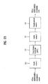
- FIG. 23 is a view showing an embodiment of a modulator
- FIG. 24 is a view showing an embodiment of an analog processor 160
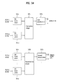
- FIG. 25 is a view showing an embodiment of a signal receiving apparatus capable of receiving a signal frame
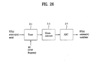
- FIG. 26 is a view showing an embodiment of a signal receiver
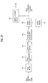
- FIG. 27 is a view showing an embodiment of a demodulator
- FIG. 28 is a view showing a multi-path signal decoder
- FIG. 29 is a view showing an embodiment of a frame parser
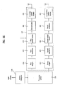
- FIG. 30 is a view showing an embodiment of each of symbol demappers 247a and 247p;
- FIG. 31 is a view showing another embodiment of each of the symbol demappers 247a and 247p;
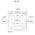
- FIG. 32 is a view showing an embodiment of multiplexing a demultiplexed sub stream
- FIG. 33 is a view showing an example of a decoding and demodulation unit
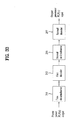
- FIG. 34 is a view showing an embodiment of an output processor
- FIG. 35 is a view showing another embodiment of a signal transmitting apparatus for transmitting a signal frame
- FIG. 36 is a view showing another embodiment of a signal receiving apparatus for receiving a signal frame
- FIG. 37 is a view showing an embodiment of a method for transmitting a signal.
- FIG. 38 is a view showing an embodiment of a method for receiving a signal.
- service is indicative of either broadcast contents which can be transmitted/received by the signal transmission/reception apparatus, or content provision.
- FIG. 1 shows a signal frame for transmitting a service according to the present invention.
- the signal frame shown in FIG. 1 shows an exemplary signal frame for transmitting a broadcast service including audio/video (A/V) streams.
- a single service is multiplexed in time- and frequency- channels, and the multiplexed service is transmitted.
- the above-mentioned signal transmission scheme is called a time-frequency slicing (TFS) scheme.
- TFS time-frequency slicing
- the signal transmission apparatus according to the present invention transmits the signal service via at least one RF band (possibly several RF bands), such that it can acquire a statistical multiplexing gain capable of transmitting many more services.
- the signal transmission/reception apparatus transmits/receives a single service over several RF channels, such that it can acquire a frequency diversity gain.
- First to third services are transmitted to four RF bands (RF1 ⁇ RF4).
- RF1 ⁇ RF4 RF bands
- Two reference signals i.e., a first pilot signal (P1) and a second pilot signal (P2)
- P1 and P2 are located at the beginning part of the signal frame.
- the RF1 band includes three slots associated with the Service 1, two slots associated with the Service 2, and a single slot associated with the Service 3. Slots associated with other services may also be located in other slots (Slots 4 ⁇ 17) located after the single slot associated with the Service 3.
- the RF2 band includes a first pilot signal (P1), a second pilot signal (P2), and other slots 13 - 17.
- the RF2 band includes three slots associated with the Service 1, two slots associated with the Service 2, and a single slot associated with the Service 3.
- the Services 1 ⁇ 3 are multiplexed, and are then transmitted to the RF3 and RF4 bands according to the time-frequency slicing (TFS) scheme.
- the modulation scheme for signal transmission may be based on an orthogonal frequency division multiplexing (OFDM) scheme.
- a super-frame can be composed of several signal frames.
- a future extension frame may also be located among the several signal frames. If the future extension frame is located among the several signal frames, the super-frame may be terminated at the future extension frame.
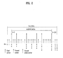
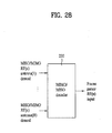
- FIG. 2 shows a first pilot signal (P1) contained in the signal frame of FIG. 1 according to the present invention.
- the first pilot signal P1 and the second pilot signal P2 are located at the beginning part of the signal frame.
- the first pilot signal P1 is modulated by a 2K FFT mode, and may be transmitted simultaneously while including a 1/4 guard interval.
- a band of 7.61Mhz of the first pilot signal P1 includes a band of 6.82992Mhz.
- the first pilot signal uses 256 carriers from among 1705 active carriers. A single active carrier is used for every 6 carriers on average. Data-carrier intervals may be irregularly arranged in the order of 3, 6, and 9.
- a solid line indicates the location of a used carrier
- a thin dotted line indicates the location of an unused carrier
- a chain line indicates a center location of the unused carrier.
- the used carrier can be symbol-mapped by a binary phase shift keying (BPSK), and a pseudo-random bit sequence (PRBS) can be modulated.
- BPSK binary phase shift keying
- PRBS pseudo-random bit sequence
- the size of a FFT used for the second pilot signal can be indicated by several PRBSs.
- the signal reception apparatus detects a structure of a pilot signal, and recognizes a time-frequency slicing (TFS) using the detected structure.
- the signal reception apparatus acquires the FFT size of the second pilot signal, compensates for a coarse frequency offset of a reception signal, and acquires time synchronization.
- a signal transmission type and a transmission parameter may be set.
- the second pilot signal P2 may be transmitted with a FFT size and a guard interval equal to those of the data symbol.
- a single carrier is used as a pilot carrier at intervals of three carriers.
- the signal reception apparatus compensates for a fine frequency synchronization offset using the second pilot signal, and performs fine time synchronization.
- the second pilot signal transmits information of a first layer (L1) from among Open Systems Interconnection (OSI) layers.
- the second pilot signal may include a physical parameter and frame construction information.
- the second pilot signal transmits a parameter value by which a receiver can access a Physical Layer Pipe (PLP) service stream.
- PLP Physical Layer Pipe
- L1 (Layer 1) information contained in the second pilot signal P2 is as follows.
- the Layer-1 (L1) information includes a length indicator indicating the length of data including the L1 information, such that it can easily use the signaling channels of Layers 1 and 2 (L1 and L2).
- the Layer-1 (L1) information includes a frequency indicator, a guard-interval length, a maximum number of FEC (Forward Error Correction) blocks for each frame in association with individual physical channels, and the number of actual FEC blocks to be contained in the FEC block buffer associated with a current/previous frame in each physical channel.
- the frequency indicator indicates frequency information corresponding to the RF channel.
- the Layer-1 (L1) information may include a variety of information in association with individual slots.
- the Layer-1 (L1) information includes the number of frames associated with a service, a start address of a slot having the accuracy of an OFDM carrier contained in an OFDM symbol, a length of the slot, slots corresponding to the OFDM carrier, the number of bits padded in the last OFDM carrier, service modulation information, service mode rate information, and Multi-Input-Multi-Output (MIMO) scheme information.
- MIMO Multi-Input-Multi-Output
- the Layer-1 (L1) information may include a cell ID, a flag for service like notification message service(e.g., an emergency message), the number of current frames, and the number of additional bits for future use.
- the cell ID indicates a broadcast area transmitted by a broadcast transmitter
- the second pilot signal P2 is adapted to perform channel estimation for decoding a symbol contained in the P2 signal.
- the second pilot signal P2 can be used as an initial value for channel estimation for the next data symbol.
- the second pilot signal P2 may also transmit Layer-2 (L2) information.
- L2 Layer-2
- the second pilot signal is able to describe information associated with the transmission service in Layer-2 (L2) information.
- the signal transmission apparatus decodes the second pilot signal, such that it can acquire service information contained in the time-frequency slicing (TFS) frame and can effectively perform the channel scanning.
- this Layer-2 (L2) information may be included in a specific PLP of the TFS frame.
- L2 information can be included in a specific PLP, and the service description information also can be transmitted in the specific PLP.
- the second pilot signal may include two OFDM symbols of the 8k FFT mode.
- the second pilot signal may be any one of a single OFDM symbol of the 32K FFT mode, a single OFDM symbol of the 16k FFT mode, two OFDM symbols of the 8k FFT mode, four OFDM symbols of the 4k FFT mode, and eight OFDM symbols of the 2k FFT mode.
- a single OFDM symbol having the size of a large FFT or several OFDM symbols, each of which has the size of a small FFT, may be contained in the second pilot signal P2, such that capacity capable of being transmitted to the pilot can be maintained.
- L1 (Layer1) and L2 (Layer2) information contained in the second pilot signal is error-correction-coded and is then interleaved, such that data recovery is carried out although an impulse noise occurs.
- L2 information can also be included in a specific PLP conveying the service description information.
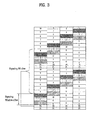
- FIG. 3 shows a signaling window according to the present invention.
- the time-frequency slicing (TFS) frame shows an offset concept of the signaling information.
- Layer-1 (L1) information contained in the second pilot signal includes frame construction information and physical layer information required by the signal reception apparatus decoding the data symbol. Therefore, if information of the following data symbols located after the second pilot signal, is contained in the second pilot signal, and the resultant second pilot signal is transmitted, the signal reception apparatus may be unable to immediately decode the above following data symbols due to a decoding time of the second pilot signal.
- the L1 information contained in the second pilot signal includes information of a single time-frequency slicing (TFS) frame size, and includes information contained in the signaling window at a location spaced apart from the second pilot signal by the signaling window offset.
- TFS time-frequency slicing
- the data symbol may include a scatter pilot and a continual pilot.
- the signal transmission/reception system capable of transmitting/receiving signal frames shown in FIGS. 1 ⁇ 3 will hereinafter be described.
- Individual services can be transmitted and received over several RF channels.
- a path for transmitting each of the services or a stream transmitted via this path is called a PLP.
- the PLP may be distributed among the timely-divided slots in several RF channels or a single RF band.
- This signal frame can convey the timely-divided PLP in at least one RF channel.
- a sigle PLP can be transferred through at least one RF channel with timely-divided regions.
- the signal transmission/receiption systems transmitting/receiving a signal frame via at least one RF band will be disclosed.
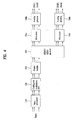
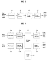
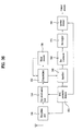
- FIG. 4 is a block diagram illustrating an apparatus for transmitting a signal according to one embodiment of the present invention.
- the signal transmission apparatus includes an input processor 110, a coding and modulation unit 120, a frame builder 130, a MIMO/MISO encoder 140, a plurality of modulators (150a, ..., 150r) of the MIMO/MISO encoder 140, and a plurality of analog processors (160a,...,160r).
- the input processor 110 receives streams equipped with several services, generates P number of baseband frames (P is a natural number) which includes modulation- and coding- information corresponding to transmission paths of the individual services, and outputs the P number of baseband frames.
- P is a natural number
- the coding and modulation unit 120 receives baseband frames from the input processor 110, performs the channel coding and interleaving on each of the baseband frames, and outputs the channel coding and interleaving result.
- the frame builder 130 forms frames which transmit baseband frames contained in P number of PLPs to R number of RF channels (where R is a natural number), splits the formed frames, and outputs the split frames to paths corresponding to the R number of RF channels.
- R is a natural number
- the signal frames generated from the frame builder 140 may include a time-frequency slicing (TFS) structure in which the service is multiplexed in time- and frequency- domains.
- TFS time-frequency slicing
- the MIMO/MISO encoder 140 encodes signals to be transmitted to the R number of RF channels, and outputs the coded signals to paths corresponding to A number of antennas (where A is a natural number).
- the MIMO/MISO encoder 140 outputs the coded signal in which a single to be transmitted to a single RF channel is encoded to the A number of antennas, such that a signal is transmitted/received to/from a MIMO (Multi-Input-Multi-Output) or MISO (Multi-Input-Single-Output) structure.
- the modulators (150a, ..., 150r) modulate frequency-domain signals entered via the path corresponding to each RF channel into time-domain signals.
- the modulators (150a, ..., 150r) modulate the input signals according to an orthogonal frequency division multiplexing (OFDM) scheme, and outputs the modulated signals.
- OFDM orthogonal frequency division multiplexing
- the analog processors (160a, ..., 160r) converts the input signals into RF signals, such that the RF signals can be outputted to the RF channels.
- the signal transmission apparatus may include a predetermined number of modulators (150a,...150r) corresponding to the number of RF channels and a predetermined number of analog processors (160a,...,160r) corresponding to the number of RF channels.
- the number of analog processors must be equal to the product of R (i.e., the number of RF channels) and A (i.e., the number of antennas).
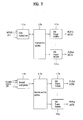
- FIG. 5 is a block diagram illustrating an input processor 110 according to the present invention.
- the input processor 110 includes the first stream multiplexer 111a, the first service splitter 113a, and a plurality of first baseband (BB) frame builders (115a, ..., 115m).
- the input processor 110 includes a second stream multiplexer 111b, a second service splitter 113b, and a plurality of second baseband (BB) frame builders (115n, ..., 115p).
- BB baseband
- the first stream multiplexer 111a receives several MPEG-2 transport streams (TSs), multiplexes the received MPEG-2 TS streams, and outputs the multiplexed MPEG-2 TS streams.
- the first service splitter 113a receives the multiplexed streams, splits the input streams of individual services, and outputs the split streams.
- the service transmitted via a physical-channel path is called a PLP
- the first service splitter 113a splits the service to be transmitted to each PLP, and outputs the split service.
- the first BB frame builders (115a, ..., 115m) build data contained in a service to be transmitted to each PLP in the form of a specific frame, and output the specific-frame-formatted data.
- the first BB frame builders (115a, ..., 115m) build a frame including a header and payload equipped with service data.
- the header of each frame may include mode information based on the modulation and encoding of the service data, and a counter value based on a clock rate of the modulator to synchronize input streams.
- the second stream multiplexer 111b receives several streams, multiplexes input streams, and outputs the multiplexed streams.
- the second stream multiplexer 111b may multiplex Internet Protocol (IP) streams instead of the MPEG-2 TS streams.
- IP Internet Protocol
- GSE generic stream encapsulation
- the streams multiplexed by the second stream multiplexer 111 b may be any one of streams. Therefore, the above-mentioned streams different from the MPEG-2 TS streams are called generic streams (GS streams).
- the second service splitter 113b receives the multiplexed generic streams, splits the received generic streams according to individual services (i.e., PLP types), and outputs the split GS streams.
- the second BB frame builders (115n, ..., 115p) build service data to be transmitted to individual PLPs in the form of a specific frame used as a signal processing unit, and output the resultant service data.
- the frame format built by the second BB frame builders (115n, ..., 115p) may be equal to that of the first BB frame builders (115a, ..., 115m) as necessary. If required, another embodiment may also be proposed. In another embodiment, the frame format built by the second BB frame builders (115n, ..., 115p) may be different from that of the first BB frame builders (115a, ..., 115m).
- the MPEG-2 TS header further includes a Packet Syncword which is not contained in the GS stream, resulting in the occurrence of different headers.
- FIG. 6 is a block diagram illustrating a coding and modulation unit according to the present invention.
- the coding and modulation unit includes a first interleaver 123, a second encoder 125, and a second interleaver 127.
- the first encoder 121 acts as an outer coder of the input baseband frame, and is able to perform the error correction encoding.
- the first encoder 121 performs the error correction encoding of the input baseband frame using a Bose- Chaudhuri-Hocquenghem (BCH) scheme.
- BCH Bose- Chaudhuri-Hocquenghem
- the first interleaver 123 performs interleaving of the encoded data, such that it prevents a burst error from being generated in a transmission signal.
- the first interleaver 123 may not be contained in the above-mentioned embodiment.
- the second encoder 125 acts as an inner coder of either the output data of the first encoder 121 or the output data of the first interleaver 123, and is able to perform the error correction encoding.
- a low density parity bit (LDPC) scheme may be used as an error correction encoding scheme.
- the second interleaver 127 mixes the error-correction-encoded data generated from the second encoder 125, and outputs the mixed data.
- the first interleaver 123 and the second interleaver 127 are able to perform interleaving of data in units of a bit.
- the coding and modulation unit 120 relates to a single PLP stream.
- the PLP stream is error-correction-encoded and modulated by the coding and modulation unit 120, and is then transmitted to the frame builder 130.
- FIG. 7 is a block diagram illustrating a frame builder according to the present invention.
- the frame builder 130 receives streams of several paths from the coding and modulation unit 120, and arranges the received streams in a single signal frame.
- the frame builder may include a first mapper 131a and a first time interleaver 132a in a first path, and may include a second mapper 131 b and a second time interleaver 132b in a second path.
- the number of input paths is equal to the number of PLPs for service transmission or the number of streams transmitted via each PLP.
- the first mapper 131a performs mapping of data contained in the input stream according to the first symbol mapping scheme.
- the first mapper 131a may perform mapping of the input data using a QAM scheme (e.g., 16 QAM, 64 QAM, and 256 QAM).
- the input data may be mapped to several kinds of symbols according to several symbol mapping schemes.
- the first mapper 131 a classifies the input data into a baseband-frame unit and a baseband-frame sub-unit. Individual classified data may be hybrid-symbol-mapped by at least two QAM schemes (e.g., 16 QAM and 64 QAM). Therefore, data contained in a single service may be mapped to symbols based on different symbol mapping schemes in individual intervals.
- the first time interleaver 132a receives a symbol sequence mapped by the first mapper 131a, and is able to perform the interleaving in a time domain.
- the first mapper 131 a maps data, which is contained in the error-corrected frame unit received from the coding and modulation unit 120, into symbols.
- the first time interleaver 132a receives the symbol sequence mapped by the first mapper 131a, and interleaves the received symbol sequence in units of the error-corrected frame.
- the p-th mapper 131 p or the p-th time interleaver 132p receives service data to be transmitted to the p-th PLP, maps the service data into symbols according to the p-th symbol mapping scheme.
- the mapped symbols can be interleaved in a time domain. It should be noted that this symbol mapping scheme and this interleaving scheme are equal to those of the first time interleaver 132a and the first mapper 131 a.
- the symbol mapping scheme of the first mapper 131 a may be equal to or different from that of the p-th mapper 131 p.
- the first mapper 131 a and the p-th mapper 131 p are able to map input data to individual symbols using the same or different hybrid symbol mapping schemes.
- Data of the time interleavers located at individual paths i.e., service data interleaved by the first time interleaver 132a and service data to be transmitted to R number of RF channels by the p-th time interleaver 132p
- the physical channel allows the above data to be interleaved over several RF channels.
- the TFS frame builder 133 In association with streams received in as many paths as the number of PLPs, the TFS frame builder 133 builds the TFS signal frame such as the above-mentioned signal frame, such that the service is time-shifted according to RF channels.
- the TFS frame builder 133 splits service data received in any one of paths, and outputs the service data split into data of the R number of RF bands according to a signal scheduling scheme.
- the TFS frame builder 133 receives the first pilot signal and the second pilot signal from the signaling information unit (denoted by Ref/PL signal) 135, arranges the first and second pilot signals in the signal frame, and inserts the signaling signal (L1 and L2) of the above-mentioned physical layer in the second pilot signal.
- the first and second pilot signals are used as the beginning signals of the signal frame contained in each RF channel from among the TFS signal frame received from the signaling information unit (Ref/PL signal) 135.
- the first pilot signal may include a transmission type and basic transmission parameters
- the second pilot signal may include a physical parameter and frame construction information.
- the second pilot signal includes a L1 (Layer 1) signaling signal and a L2 (Layer 2) signaling signal.
- the R number of frequency interleavers (137a, ..., 137r) interleave service data, to be transmitted to corresponding RF channels of the TFS signal frame, in a frequency domain.
- the frequency interleavers (137a, ..., 137r) can interleave the service data at a level of data cells contained in an OFDM symbol.
- service data to be transmitted to each RF channel in the TFS signal frame is frequency-selective-fading-processed, such that it may not be lost in a specific frequency domain.
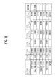
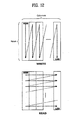
- FIG. 8 is a view showing a first example of a ratio of symbols when the mappers 131a and 131b perform hybrid symbol mapping.
- This Figure shows the number of bits transmitted by one sub carrier (cell) if error correction coding is performed by the coding and modulation unit in a normal mode (the length of the error-correction-coded code is 64800 bits) of LDPC error correction coding mode.
- mappers 131 a and 131 b perform symbol mapping using 256QAM, 64800 bits are mapped to 8100 symbols. If the mappers 131 a and 131 b perform hybrid symbol mapping (Hyb 128-QAM) using 256QAM and 64QAM with a ratio of 3:2, the number of symbols mapped by 256QAM is 4860 and the number of symbols mapped by 64QAM is 4320. The number of transmitted bits per sub carrier (cell) is 7.0588.
- the data is mapped to 16200 symbols, each of which is used to transmit four bits.
- the data may be mapped to 32400 symbols, each of which is used to transmit two bits.
- FIG. 9 shows symbol mapping methods of error-corrected data by LDPC error correction coding method of a short mode (the length of the error-correction-coded code is 16200 bits), which are equal to the symbol mapping methods of FIG. 8 , and the numbers of bits per sub carrier according to the symbol mapping methods.
- the numbers of bits transmitted by the sub carrier is equal to those of the normal mode (64800 bits) according to the symbol mapping methods such as 256QAM, Hyb 128-QAM, 64-QAM, Hyb 32-QAM, 16QAM, Hyb8-QAM and QPSK, but the total numbers of symbols transmitted are different from those of the normal mode. For example, 16200 bits are transmitted by 2025 symbols in 256QAM, 16200 bits are transmitted by 1215 symbols according to 256QAM and 1080 symbols according to 64QAM (total 2295 symbols) in Hyb 128-QAM.
- a data transmission rate per sub carrier (cell) for each PLP may be adjusted according to a hybrid symbol mapping method or a single symbol mapping method.
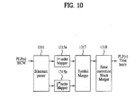
- FIG. 10 is a view showing an example of each of the symbol mappers 131a and 131 b shown in FIG. 7 .
- Each of the symbol mappers 131 a and 131 b includes a first order mapper 1315a, a second order mapper 131b, a symbol merger 1317 and an error correction block merger 1318.
- the bit stream parser 1311 receives the PLP service stream from the coding and modulation unit and splits the received service stream.
- the first order symbol mapper 1315a maps the bits of the service stream split by a higher order symbol mapping method to symbols.
- the second order symbol mapper 1315b maps the bits of the service stream split by a lower order symbol mapping method to symbols.
- the first order symbol mapper 1315a may map the bit stream to symbols according to 256QAM and the second order symbol mapper 1315b may map the bit stream to symbols according to 64QAM.
- the symbol merger 1317 merges the symbols output from the symbol mappers 1315a and 1315b to one symbol stream and outputs the symbol stream.
- the symbol merger 1317 may output the symbol stream included in one PLP.
- the error correction block merger 1318 may output one symbol stream merged by the symbol merger 1317 in the error-correction-coded code block unit.
- the error correction block merger 1318 may output a symbol block such that the error-correction-coded code blocks are uniformly allocated to at least one RF band of the TFS signal frame.
- the error correction block merger 1318 may output the symbol block such that the length of the symbol block of the error-correction-coded block of a normal mode is equal to that of the symbol block of the error-correction-coded block of a short mode. For example, four symbol blocks of the error-correction-coded block of the short mode may be merged to one symbol block.
- the error correction block merger 1318 may split the symbol stream according to a common multiple of the number of RF bands such that signal frame builder uniformly arranges the symbols to the RF bands. If the maximum number of RF bands in the signal frame is 6, the error correction block merger 1318 outputs the symbol block such that the total number of symbols can be divided by 60 which is a common multiple of 1, 2, 3, 4, 5 and 6.
- the symbols included in the output symbol block may be arranged to be uniformly allocated to the six RF bands. Accordingly, although an error correction mode according to a code rate and a symbol mapping method are combined, the symbols configuring the PLP are uniformly allocated to the RF bands.
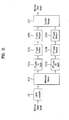
- FIG. 11 is a view showing another embodiment of the symbol mapper.
- the symbol mapper includes the second encoder 125 and the second interleaver 127 included in the coding and modulation unit. That is, if this embodiment is used, the coding and modulation unit may include only the first encoder 121, the first interleaver 123 and the second encoder 125.
- the embodiment of the symbol mapper includes a bit stream parser 1311, a first order bit interleaver 1312a, a second order bit interleaver 1312b, a first order demux 1313a, a second order demux 1313b, a first order symbol mapper 1315a, a second order symbol mapper 1315b and a symbol merger 1317.
- the length of the error-correction-coded block may vary according to an LDPC mode. If the bits included in the error-correction-coded block are mapped to the symbols, the error correction capabilities of the bits included in a cell word configuring the symbol may vary according to the locations of the bits. For example, the cell word which is the symbol may be determined according to the code rate of the error correction coding and the symbol mapping method (whether the symbol mapping method is the higher order symbol mapping method or the lower order symbol mapping method).
- the error correction capabilities of the bits vary according to the locations of the bits in the error-correction-coded block.
- the reliabilities of the bits coded according to the characteristics of the H-matrix used in the irregular LDPC error correction coding method may vary according to the locations of the bits. Accordingly, the order of the bits configuring the cell word mapped to the symbol is changed such that the error correction capabilities of the bits which are weak against the error correction in the error-correction-coded block are adjusted and the robustness against the error in the bit level can be adjusted.
- the second encoder 125 performs the error correction coding with respect to the stream included in one PLP by the LDPC error correction coding method.
- the bit stream parser 1311 receives the service stream according to the PLP and splits the received service stream.
- the first order bit interleaver 1312a interleaves the bits included in a first bit stream of the split service streams.
- the second order bit interleaver 1312b interleaves the bits included in a second bit stream of the split service streams.
- the first order bit interleaver 1312a and the second order bit interleaver 1312b may correspond to the second interleaver 127 used as an inner interleaver.
- the interleaving method of the first order bit interleaver 1312a and the second order bit interleaver 1312b will be described later.
- the first order demux 1313a and the second order demux 1313b demultiplex the bits of the bit streams interleaved by the first order bit interleaver 1312a and the second order bit interleaver 1312b.
- the demuxs 1313a and 1313b divide the input bit stream into sub bit streams which will be mapped to a real axis and an imaginary axis of a constellation and output the sub bit streams.
- the symbol mappers 1315a and 1315b map the sub bit streams demultiplexed by the demuxs 1313a and 1313b to the corresponding symbols.
- the bit interleavers 1312a and 1312b and the demuxs 1313a and 1313b may combine the characteristics of the LDPC codeword and the characteristics of the constellation reliability of the symbol mapping according to the constellation.
- the detailed embodiment of the first order demuxs 1313a and 1313b will be described later.
- the first order symbol mapper 1315a performs first order symbol mapping, for example, higher order symbol mapping
- the second order symbol mapper 1315b performs second order symbol mapping, for example, lower order symbol mapping.
- the first order symbol mapper 1315a maps the sub bit streams output from the first order demux 1313 to the symbols
- the second order symbol mapper 1315b maps the sub bit streams output from the second order demux 1313b to the symbols.
- the symbol merger 1317 merges the symbols mapped by the first order symbol mapper 1315a and the second order symbol mapper 1315b to one symbol stream and outputs the symbol stream.
- the error correction capabilities of the bits may be changed according to the locations of the bits in the error-correction-coded block. Accordingly, if the bit interleaver and the demux are controlled according to the characteristics of the LDPC encoder 125 so as to change the order of the bits configuring the cell word, the error correction capability in the bit level can be maximized.
- FIG. 12 is a view showing the concept of interleaving of bits by the bit interleavers 1312a and 1312b of FIG. 11 .
- input bits are stored in and read from a matrix-formed memory having a predetermined number of rows and columns.
- the bits are stored in a first column in row direction, and, if the first column is filled up, the bits are stored in another column in row direction.
- the stored bits are read, the bits are read in column direction and, if all the bits stored in a first row are read, the bits in another row are read in column direction.
- the bits are stored row-wise such that the columns are filled up serially.
- the stored bits are read, the stored bits are read column-wise from the first row to last row serially.
- MSB means a most significant bit
- LSB means a least significant bit.
- the bit interleavers 1312a and 1312b may change the number of rows and columns of the memory according to the types of the symbol mappers 1315a and 1315b.
- Fig. 13 is a view showing an example of the number of rows and columns of memories of the bit interleavers 1312a and 1312b according to the types of symbol mappers 1315a and 1315b, if the LDPC mode is the normal mode.
- the first order interleaver 1312a interleaves the bits by a memory having 8100 rows and 8 columns. If the symbols are mapped by 64QAM, the first order interleaver 1312a interleaves the bits by a memory having 10800 rows and 6 columns. If the symbols are mapped by 16QAM, the first order interleaver 1312a interleaves the bits by a memory having 16200 rows and 4 columns.
- the first order interleaver 1312a interleaves the bits using a memory having 4860 rows and 8 columns
- the second order interleaver 1312b interleaves the bits using a memory having 4320 rows and 6 columns.
- the symbol mappers 1315a and 1315b map the symbols by Hyb32-QAM
- the first order interleaver 1312a interleaves the bits using a memory having 6480 rows and 6 columns
- the second order interleaver 1312b interleaves the bits using a memory having 6480 rows and 4 columns.
- Fig. 14 is a view showing an example of the number of rows and columns of the memories of the bit interleavers 1312a and 1312b according to the types of the symbol mappers 1315a and 1315b, if the LDPC mode is the short mode.
- the first order interleaver 1312a interleaves the bits by a memory having 2025 rows and 8 columns. If the symbol mappers 1315a and 1315b map the symbols by Hyb128-QAM, the first order interleaver 1312a interleaves the bits using a memory having 1215 rows and 8 columns, and the second order interleaver 1312b interleaves the bits using a memory having 1080 rows and 6 columns.
- the locations of the bits in the error-correction-coded block may be changed.
- FIG. 15 is a view showing the concept of multiplexing of input bits of the demuxs 1313a and 1313b.
- the bit interleavers 1312a and 1312b interleave the input bits x0, x1, ..., and xn-1 and output the interleaved bits.
- the interleaving method is already described above.
- the demuxs 1313a and 1313b demultiplex the interleaved bit streams.
- the demultiplexing method may vary according to the code rate of the error correction coding method and the symbol mapping method of the symbol mapper. If the symbol method of the symbol mapper is QPSK, the input bits, for example, are interleaved to two sub streams and the symbol mapper maps the two sub streams to the symbols so as to correspond to the real axis and the imaginary axis of the constellation. For example, a first bit y0 of the demultiplexed first sub stream corresponds to the real axis and a first bit y1 of the demultiplexed second sub stream corresponds to the imaginary axis.
- the input bits for example, are demultiplexed to four sub frames.
- the symbol mapper selects the bits included in the four sub streams and maps the selected bits to the symbols so as to correspond to the real axis and the imaginary axis of the constellation.
- bits y0 and y2 of the demultiplexed first and third sub streams correspond to the real axis and the bits y1 and y3 of the demultiplexed second and fourth sub streams correspond to the imaginary axis.
- the input bits may be demultiplexed to six bit streams.
- the symbol mapper maps the six sub streams to the symbols so as to correspond to the real axis and the imaginary axis of the constellation.
- the demultiplexed first, third and fifth sub stream bits y0, y2 and y4 correspond to the real axis
- the demultiplexed second, fourth and sixth sub stream bits y1, y3 and y6 correspond to the imaginary axis.
- the input bits may be demultiplexed to eight bit streams.
- the symbol mapper maps the eight sub streams to the symbols so as to correspond to the real axis and the imaginary axis of the constellation. For example, first, the demultiplexed first, third fifth and seventh sub stream bits y0, y2, y4 and y6 correspond to the real axis and the demultiplexed second, fourth, sixth and eighth sub stream bits y1, y3, y6 and y7 correspond to the imaginary axis.
- the sub streams demultiplexed by the demux may be mapped to the bit streams of the real axis and the imaginary axis of the constellation.
- bit interleaving method demultiplexing method and symbol mapping method are exemplary and various methods may be used as the method of selecting the bits in the sub streams such that the sub streams demultiplexed by the demux may correspond to the real axis and the imaginary axis of the constellation.
- the cell word mapped to the symbols may vary according to any one of the error-corrected bit streams according to the code rate, the method of interleaving the bit streams, the demultiplexing method and the symbol mapping method.
- the MSB of the cell word is higher than the LSB of the cell word in the reliability of the error correction decoding. Although the reliability of the bit of a specific location of the error-correction-coded block is low, the reliability of the bit can be improved by the symbol demapping process if the bit of the cell word is arranged on the MSB or close to the MSB.
- the bit can be robustly transmitted/received by the symbol mapping and demapping process and the system performance can be adjusted.
- FIG. 16 is a view showing an embodiment of demultiplexing an input stream by the demux.
- the symbol mapping method is QPSK, two bits are mapped to one symbol and the two bits of one symbol unit are demultiplexed in order of the bit indexes (indexes 0 and 1 of b).
- the symbol mapping method is 16QAM, 4 bits are mapped to one symbol and the four bits of one symbol unit are demultiplexed according to the calculating result of the modulo-4 of bit indexes (indexes 0, 1, 2 and 3 of b).
- the symbol mapping method is 64QAM, 6 bits are mapped to one symbol and the six bits of one symbol unit are demultiplexed according to the calculating result of the modulo-6 of bit indexes (indexes 0, 1, 2, 3, 4 and 5 of b).
- the symbol mapping method is 256QAM, 8 bits are mapped to one symbol and the eight bits of one symbol unit are demultiplexed according to the calculating result of the modulo-8 of bit indexes (indexes 0, 1, 2, 3, 4, 5, 6 and 7 of b).
- the demultiplexing order of the sub streams is exemplary and may be modified.
- FIG. 17 is a view showing an example of a demultiplexing type according to a symbol mapping method.
- the symbol mapping method includes QPSK, 16QAM, 64QAM and 256QAM, and the demultiplexing type includes a first type to a sixth type.
- the first type is an example in which the input bits sequentially correspond to even-numbered indexes (0, 2, 4, 8, ...) (or the real axis of the constellation) and sequentially correspond to odd-numbered indexes (1, 3, 5, 7, ...) (or the imaginary axis of the constellation).
- the bit demultiplexing of the first type may be represented by a demultiplexing identifier 10 (a binary number of 1010; the location of 1 is the location of the MSB corresponding to the real axis and the imaginary axis of the constellation).
- the second type is an example in which the demultiplexing is performed in reverse order of the first type, that is, the LSB of the input bits seqentually correspond to even-numbered indexes (6, 4, 2, 0) (or the real axis of the constellation) and odd-numbered indexes (1, 3, 5, 7, ...) (or the imaginery axis of the constellation).
- the bit demultiplexing of the second type may be represented by a demultiplexing identifier 5 (a binary number of 0101).
- the third type is an example in which the input bits are arranged such that the bits of the both ends of the codeword become the MSB.
- the input bits are rearranged so as to fill the code word from the both ends of the code word.
- the bit demultiplexing of the third type may be represented by a demultiplexing identifier 9 (a binary number of 1001).
- the fourth type is an example in which the input bits are arranged such that a middle bit of the code word becomes the MSB. A bit of the input bits is first filled in the middle location of the code word and the remaining bits are then rearranged toward the both ends of the code word in order of the input bits.
- the bit demultiplexing of the fourth type may be represented by a demultiplexing identifier 6 (a binary number of 0110).
- the fifth type is an example in which the bits are demultiplexed such that a last bit of the code word becomes the MSB and a first bit thereof becomes the LSB
- the sixth type is an example in which the bits are rearranged such that the first bit of the code word becomes the MSB and the last bit thereof becomes the LSB.
- the bit demultiplexing of the fifth type may be represented by a demultiplexing identifier 3 (a binary number of 0011)
- the bit demultiplexing of the sixth type may be represented by a demultiplexing identifier 12 (a binary number of 1100).
- the demultiplexing type may vary according to the symbol mapping method or the code rate of the error correction coding method. That is, a different demultiplexing type may be used if the symbol mapping method or the code rate is changed.
- FIG. 18 is a view showing an embodiment of demultiplexing an input bit stream according to a demultiplexing type. This embodiment may include bit interleavers 1312a and 1312b, demuxs 1313a and 1313b and mappers 1315a and 1315b.
- the bit interleavers 1312a and 1312b interleave the error-correction-coded PLP service streams.
- the bit interleavers 1312a and 1312b may perform the bit interleaving in the error correction coding units according to the error correction coding mode.
- the bit interleaving method is already described above.
- the demuxs 1313a and 1313b may include first type demuxs 1313a1 and 1313b1, ..., and n th type demuxs 1313a2 and 1313b2.
- n is an integer.
- the methods of demultiplexing the bits by the n types of demuxs follow the types shown in FIG. 17 .
- the first type demuxs may correspond to the first type bit demultiplexing (1100) and the second type demux (not shown) may correspond to the second type bit demultiplexing (0011).
- the n th type demux 1313b demultiplexes the input bit stream according to the n th type bit multiplexing (e.g., the demultiplexing identifier 1100) and outputs the demultiplexed bit stream.
- Selectors 1313a3 and 1313b3 receive a demux selection signal of the demultiplexing type suitable for the input bits and output the demultiplexed bit stream according to any one of the first type to the n th type and the demux selection signal.
- the demux selection signal may vary according to the code rate of the error correction coding and the symbol mapping method of the constellation. Accordingly, the demultiplexing type may be determined according to the code rate of the error correction coding method or/and the symbol mapping method of the constellation. The detailed example according to the symbols mapped to the constellation or/and the code rate of the error correction coding according to the demux selection signal will be described later.
- the mappers 1315a and 1315b may map the demultiplexed sub bit streams to the symbols according to the demux selection signal and output the mapped symbols.
- FIG. 19 is a view showing a demultiplexing type which is determined according to a code rate of the error correction coding and the symbol mapping method.
- the bit stream can be demultiplexed according to all the demultiplexing types (denoted by all).
- the code rate of the LDPC error correction coding method is 1/4, 1/3, 2/5 and 1/2, the symbols can be mapped without performing the bit interleaving and the bit demultiplexing (denoted by No-Int and No-Demux). If the code rate of the error correction coding is 3/5, the bit can be demultiplexed according to any one of the demultiplexing identifiers 9, 10 and 12. If the code rate of the error correction coding is 2/3, 3/4, 4/5, 5/6, 8/9 and 9/10, the input bit stream can be demultiplexed according to the demultiplexing identifier 6.
- the code rate of the LDPC error correction coding is 1/4, 1/3, 2/5 and 1/2
- the symbols can be mapped without performing the bit interleaving and the bit demultiplexing.
- the code rate is 3/5
- the bits can be demultiplexed according to any one of the demultiplexing identifiers 9 and 10.
- the code rate is 2/3, 3/4, 4/5, 5/6, 8/9 and 9/10
- the bits can be demultiplexed according to the demultiplexing identifier 6.
- the code rate of the LDPC error correction coding is 1/4, 1/3, 2/5 and 1/2
- the symbols can be mapped without performing the bit interleaving and the bit demultiplexing.
- the code rate is 3/5
- the bits can be demultiplexed according to the demultiplexing identifier 9.
- the code rate is 2/3, 3/4, 4/5, 5/6, 8/9 and 9/10
- the bits can be demultiplexed according to the demultiplexing identifier 6.
- the bit demultiplexing type may vary according to the code rate used for the error correction coding and the symbol mapping method. Accordingly, the error correction capability of a bit located on a specific location of the error-correction-coded block may be adjusted by mapping the demultiplexed sub streams to the symbols. Accordingly it is possible to optimize the robustness in the bit level.
- FIG. 20 is a view showing an example of expressing the demultiplexing method by an equation.
- the symbol mapping method is QPSK
- the input bits (x i , XN/2+i ) correspond to the demultiplexed bits y0 and y1.
- the symbol mapping method is 16QAM
- the input bits x 2 ⁇ N 4 + i ⁇ x 3 ⁇ N 4 + i ⁇ x i ⁇ x n 4 + i correspond to the demultiplexed bits y0, y1, y2 and y3.
- the input bits x 4 ⁇ N 6 + i ⁇ x 5 ⁇ N 6 + i ⁇ x 2 ⁇ N 6 + i ⁇ x 3 ⁇ N 6 + i ⁇ x i ⁇ x N 6 + i correspond to the demultiplexed bits y0, y1, y2, y3, y4 and y5.
- the input bits x 6 ⁇ N 8 + i ⁇ x 7 ⁇ N 8 + i ⁇ x 4 ⁇ N 8 + i ⁇ x 5 ⁇ N 8 + i ⁇ x 2 ⁇ N 8 + i ⁇ x 3 ⁇ N 8 + i ⁇ x i ⁇ x N 8 + i correspond to the demultiplexed bits y0, y1, y2, y3, y4, y5, y6 and y7.
- N denotes the number of bits mapped to the symbols with respect to the input of the bit interleaver.
- FIG. 21 is a view showing an example of mapping a symbol by a symbol mapper.
- the symbols on the constellation correspond to the value of the bit y0 of the demultiplexed first sub stream and the value of the bit y1 of the demultiplexed second sub stream.
- the real axis of the symbols on the constellation corresponds to the bits of the demultiplexed first and third sub streams (bits separated from the location of the MSB by 0 and 2) and the imaginary axis thereof corresponds to the bits of the demultiplexed second and fourth sub streams (bits separated from the location of the MSB by 1 and 3).
- the real axis of the symbols on the constellation corresponds to the bits of the demultiplexed first, third, and fifth sub streams (bits separated from the location of the MSB by 0, 2 and 4) and the imaginary axis thereof corresponds to the bits of the demultiplexed second, fourth and sixth sub streams (bits separated from the location of the MSB by 1, 3 and 5).
- the bits configuring the symbol may be mapped to the cell word in the demultiplexing order. If the bits configuring the cell word are demultiplexed, the MSB and the LSB of the cell word are changed and the robustness of the bits can be adjusted although the reliabilities of the LDPC error-correction-coded bits vary according to the locations.
- FIG. 22 is a block diagram illustrating a MIMO/MISO encoder according to the present invention.
- the MIMO/MISO encoder encodes the input data using the MIMO/MISO encoding scheme, and outputs the encoded data to several paths. If a signal reception end receives the signal transmitted to the several paths from one or more paths, it is able to acquire a gain (also called a diversity gain, a payload gain, or a multiplexing gain).
- a gain also called a diversity gain, a payload gain, or a multiplexing gain.
- the MIMO/MISO encoder 140 encodes service data of each path generated from the frame builder 130, and outputs the encoded data to the A number of paths corresponding to the number of output antennas.
- FIG. 23 is a block diagram illustrating a modulator according to the present invention.
- the modulator includes a first power controller (PAPR Reduce1) 151, a time-domain transform unit (IFFT) 153, a second power controller (PAPR Reduce2) 157, and a guard-interval inserter 159.
- PAPR Reduce1 first power controller
- IFFT time-domain transform unit
- PAPR Reduce2 second power controller
- guard-interval inserter 159 a guard-interval inserter 159.
- the first power controller 151 reduces a PAPR (Peak-to-Average Power Ratio) of data transmitted to the R number of signal paths in the frequency domain.
- PAPR Peak-to-Average Power Ratio
- the time-domain transform (IFFT) unit 153 converts the received frequency-domain signals into time-domain signals.
- the frequency-domain signals may be converted into the time-domain signals according to the IFFT algorithm. Therefore, the frequency-domain data may be modulated according to the OFDM scheme.
- the second power controller (PAPR Reduce2) 157 reduces a PAPR (Peak-to-Average Power Ratio) of channel data transmitted to the R number of signal paths in the time domain.
- PAPR Peak-to-Average Power Ratio
- ACE active constellation extension
- the guard-interval inserter 159 inserts the guard interval into the output OFDM symbol, and outputs the inserted result. As described above, the above-mentioned embodiment can be carried out in each signal of the R number of paths.
- FIG. 24 is a block diagram illustrating an analog processor 160 according to the present invention.
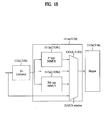
- the analog processor 160 includes a digital-to-analog converter (DAC) 161, an up-conversion unit 163, and an analog filter 165.
- DAC digital-to-analog converter
- the DAC 161 converts the input data into an analog signal, and outputs the analog signal.
- the up-conversion unit 163 converts a frequency domain of the analog signal into an RF area.
- the analog filter 165 filters the RF-area signal, and outputs the filtered RF signal.
- FIG. 25 is a block diagram illustrating an apparatus for receiving a signal according to the present invention.
- the signal reception apparatus includes a first signal receiver 210a, an n-th signal receiver 210n, a first demodulator 220a, an n-th demodulator 220n, a MIMO/MISO decoder 230, a frame parser 240, and a decoding demodulator 250, and an output processor 260.
- the receiver may include at least one signal receiver for receiving a service transmitted over at least one RF channel.
- the TFS signal frame transmitted to the R (where R is a natural number) number of RF channels can be transmitted to a multi-path via the A number of antennas.
- the A antennas have been used for the R RF channels, such that a total number of antennas is R x A.
- the first signal receiver 210a is able to receive service data transmitted via at least one path from among overall service data transmitted via several RF channels.
- the first signal receiver 210a can receive the transmission signal processed by the MIMO/MISO scheme via several paths.
- the first signal receiver 210a and the n-th signal receiver 210n can receive several service data units transmitted over n number of RF channels from among several RF channels, as a single PLP. Namely, this embodiment shows the signal reception apparatus capable of simultaneously receiving data of the R number of RF channels. Therefore, if this embodiment receives a single RF channel, only the first receiver 210a is needed.
- the first demodulator 220a and the n-th demodulator 220n demodulate signals received in the first and n-th signal receivers 210a and 210n according to the OFDM scheme, and output the demodulated signals.
- the MIMO/MISO decoder 230 decodes service data received via several transmission paths according to the MIMO/MISO decoding scheme, and outputs the decoded service data to a single transmission path. If the number R of services transmitted over several transmission paths are received, the MIMO/MISO decoder 230 can output single PLP service data contained in each of R services corresponding to the number of R channels. If P number of services are transmitted via the R number of RF channels, and signals of individual RF channels are received via the A number of antennas, the receiver decodes the P number of services using a total of (R x A) reception antennas.
- the frame parser 240 parses the TFS signal frame including several services, and outputs the parsed service data.
- the decoding demodulator 250 performs the error correction decoding on the service data contained in the parsed frame, demaps the decoded symbol data into bit data, and outputs the demapping-processed result.
- the output processor 260 decodes a stream including the demapped bit data, and outputs the decoded stream.
- each of the frame parser 240, and the decoding demodulator 250, and the output processor 260 receives several service data units as many as the number of PLPs, and performs signal processing on the received service data.
- FIG. 26 is a block diagram illustrating a signal receiver according to the present invention.
- the signal receiver may include a tuner 211, a down-converter 213, and an analog-to-digital converter (ADC) 215.
- ADC analog-to-digital converter
- the tuner 211 performs hopping of some RF channels capable of transmitting user-selected services in all RF channels when the PLP is included in several RF channels, and outputs the hopping result.
- the tuner 211 performs hopping of RF channels contained in the TFS signal frame according to input RF centerfrequencies, and at the same time tunes corresponding frequency signals, such that it outputs the tuned signals. If a signal is transmitted to A number of multi-paths, the tuner 211 performs the tuning to a corresponding RF channel, and receives reception signals via the A number of antennas.
- the down converter 213 performs down conversion of the RF frequency of the signal tuned by the tuner 211, and outputs the down-conversion result.
- the ADC 215 converts an analog signal into a digital signal.
- FIG. 27 is a block diagram illustrating a demodulator according to the present invention.
- the demodulator includes a frame detector 221, a frame synchronization unit 222, a guard-interval remover 223, a frequency-domain transform unit (FFT) 224, a channel estimator 225, a channel equalizer 226, and a signaling-information extractor 227.
- FFT frequency-domain transform unit
- the demodulator acquires service data transmitted to a single PLP stream, the following signal demodulation will be carried out. A detailed description thereof will hereinafter be described.
- the frame detector 221 identifies a delivery system of a reception signal. For example, the frame detector 221 determines whether the reception signal is a DVB-TS signal or not. And, the frame detector 221 may also determine whether a reception signal is a TFS signal frame or not.
- the frame synchronization unit 222 acquires time- and frequency- domain synchronization of the TFS signal frame.
- the guide interval controller 223 removes a guard interval located between OFDM symbols from the time domain.
- the frequency-domain converter (FFT) 224 converts a reception signal into a frequency-domain signal using the FFT algorithm, such that it acquires frequency-domain symbol data.
- the channel estimator 225 performs channel estimation of a reception channel using a pilot symbol contained in symbol data of the frequency domain.
- the channel equalizer 226 performs channel equalization of reception data using channel information estimated by the channel estimator 225.
- the signaling information extractor 227 can extract the signaling information of a physical layer established in the first and second pilot signals contained in channel-equalized reception data.
- FIG. 28 is a block diagram illustrating a MIMO/MISO decoder according to the present invention.
- the signal receiver and the demodulator are designed to process a signal received in a single path. If the signal receiver and the demodulator receive PLP service data providing a single service via several paths of several antennas, and demodulate the PLP service data, the MIMO/MIMO decoder 230 outputs the signal received in several paths as service data transmitted to a single PLP. Therefore, the MIMO/MISO decoder 230 can acquire a diversity gain and a multiplexing gain from service data received in a corresponding PLP.
- the MIMO/MISO decoder 230 receives a multi-path transmission signal from several antennas, and is able to decode a signal using a MIMO scheme capable of recovering each reception signal in the form of a single signal. Otherwise, the MIMO/MISO decoder 230 is able to recover a signal using a MIMO scheme which receives the multi-path transmission signal from a single antenna and recovers the received multi-path transmission signal.
- the MIMO/MISO decoder 230 can decode signals received via the A number of antennas of individual RF channels. If the A value is equal to "1", the signals can be decoded by the MISO scheme. If the A value is higher than "1", the signals can be decoded by the MIMO scheme.
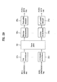
- FIG. 29 is a block diagram illustrating a frame parser according to the present invention.
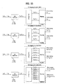
- the frame parser includes a first frequency de-interleaver 241 a, a r-th frequency de-interleaver 241 r, a frame parser 243, a first time de-interleaver 245a, a p-th time de-interleaver 245p, a first symbol demapper 247a, and a p-th symbol demapper.
- the value of "r” can be decided by the number of RF channels
- the value of "p" can be decided by the number of streams transmitting PLP service data generated from the frame parser 243.
- the frame parser includes the r number of frequency de-interleavers, the p number of time de-interleavers, and the p number of symbol demappers.
- the first frequency interleaver 241 a In association with a first RF channel, the first frequency interleaver 241 a performs de-interleaving of frequency-domain input data, and outputs the de-interleaving result.
- the frame parser 243 parses the TFS signal frame transmitted to several RF channels using scheduling information of the TFS signal frame, and parses PLP service data contained in the slot of a specific RF channel including a desired service.
- the frame parser 243 parses the TFS signal frame to receive specific service data distributed to several RF channels according to the TFS signal frame structure, and outputs first-path PLP service data.
- the first time de-interleaver 245a performs de-interleaving of the parsed first-path PLP service data in the time domain.
- the first symbol demapper 247a determines service data mapped to the symbol to be bit data, such that it can output a PLP stream associated with the first-path PLP service data.
- symbol data is converted into bit data, and each symbol data includes symbols based on the hybrid symbol-mapping scheme
- the p number of symbol demappers each of which includes the first symbol demapper, can determine the symbol data to be bit data using different symbol-demapping schemes in individual intervals of the input symbol data.
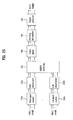
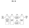
- FIG. 30 is a view showing an embodiment of each of symbol demappers 247a and 247p.
- the symbol demappers receive the streams corresponding to the PLPs from the time interleavers 245a and 245p respectively corresponding to the symbol demappers.
- Each of the symbol demappers 247a and 247p may include an error correction block splitter 2471, a symbol splitter 2473, a first order demapper 2475a, a second order demapper 2475b and a bit stream merger 2478.
- the error correction block splitter 2471 may split the PLP stream received from the corresponding one of the time interleavers 245a and 245p in the error correction block units.
- the error correction block splitter 2471 may split the service stream in the normal mode LDPC block unit.
- the service stream may be split in a state in which four blocks according to the short mode (the block having the length of 16200 bits) are treated as the error correction block of one block according to the normal mode (the block having the length of 64800 bits).
- the symbol splitter 2473 may split the symbol stream in the split error correction block according to the symbol mapping method of the symbol stream.
- the first order demapper 2475a converts the symbols according to the higher order symbol mapping method into the bits.
- the second order demapper 2475b converts the symbols according to the lower order symbol mapping method into the bits.
- the bit stream merger 2478 may receive the converted bits and output one bit stream.
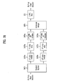
- FIG. 31 is a view showing another embodiment of each of the symbol demappers 247a and 247p.
- Each of the symbol demappers 247a and 247p may include a symbol splitter 2473, a first order demapper 2474a, a second order demapper 2474b, a first order mux 2475a, a second order mux 2475b, a first order bit deinterleaver 2476a, a second order bit deinterleaver 2476b and a bit stream merger 2478.
- the embodiment of the decoding and demodulation unit of FIG. 33 includes a first decoder 253, a first deinterleaver 255 and a second decoder 257.
- the symbol splitter 2473 may split the symbol stream of the PLP according to the method corresponding to the symbol mapping method.
- the first order demapper 2474a and the second order demapper 2474b convert the split symbol streams into bits.
- the first order demapper 2474a performs the symbol demapping of the higher order QAM and the second order demapper 2474b performs the symbol demapping of the lower order QAM.
- the first order demapper 2474a may perform the symbol demapping of 256QAM and the second order demapper 2474b may perform the symbol demapping of 64QAM.
- the first order mux 2475a and the second order mux 2475b multiplex the symbol-mapped bits.
- the multiplexing methods may correspond to the demultiplxeing methods described with reference to FIGs. 15 to 18 . Accordingly, the demultiplexed sub streams may be converted into one bit stream.
- the first order bit deinterleaver 2476a deinterleaves the bit streams multiplexed by the first order mux 2475a.
- the second order bit deinterleaver 2476b deinterleaves the bits multiplexed by the first order mux 2475a.
- the deinterleaving method corresponds to the bit interleaving method.
- the bit interleaving method is shown in FIG. 12 .
- the bit stream merger 2478 may merge the bit streams deinterleaved by the bit interleavers 2476a and 2476b to one bit stream.
- the first decoder 253 of the decoding and demodulation unit may error correction decode the output bit stream according to the normal mode or the short mode and the code rate according to the modes.
- FIG. 32 is a view showing an embodiment of multiplexing the demultiplexed sub stream.
- the demappers 2474a and 2474b decide the cell words including the bits.
- the muxs 2475a and 2475b multiplex the decided cell words according to the mux selection signal.
- the demultiplexed cell words are input to any one of first muxs 2475a2 and 2475b2 to n th muxs 2475a3 and 2475b3.
- the first muxs 2475a2 and 2475b2 to the n th muxs 2475a3 and 2475b3 change the order of the bits in the cell words input according to the mux selection signal.
- the mux selection signal may be changed according to the code rate of the error correction coding or the symbol mapping method.
- the order of selecting the sub stream may be changed according to the mux selection signal.
- the first demuxs 2475a1 and 2475b1 output the symbol-demapped bit streams to any one of the first muxs 2475a2 and 2475b2 to the n th muxs 2475a3 and 2475b3 according to the mux selection signal.
- the first sub muxs 2475a1 and 2475b1 may receive the sub streams multiplexed by the first muxs 2475a2 and 2475b2 to the n th muxs 2475a3 and 2475b3 and output one stream, according to the mux selection signal.
- the cell words including the changed bits are input to the bit interleavers 2476a and 2476b, and the bit deinterleavers 2476a and 2476b deinterleave the input bits and output the deinterleaved bits.
- FIG. 33 is a block diagram illustrating a decoding demodulator according to the present invention.
- the decoding demodulator may include several function blocks corresponding to the coding and modulation unit.
- the decoding demodulator of FIG. 16 may include a first de-interleaver 251, a first decoder 253, a second de-interleaver 255, and a second decoder 257.
- the second de-interleaver 255 can be selectively contained in the decoding demodulator.
- the first de-interleaver 251 acts as an inner de-interleaver, and is able to perform de-interleaving of the p-th PLP stream generated from the frame parser.
- the first decoder 253 acts as an inner decoder, can perform error correction of the de-interleaved data, and can use an error correction decoding algorithm based on the LDPC scheme.
- the second de-interleaver 255 acts as an outer interleaver, and can perform de-interleaving of the error- correction-decoded data.
- the second decoder 257 acts as an outer decoder. Data de-interleaved by the second de-interleaver 255 or error-corrected by the first decoder 253 is error-corrected again, such that the second decoder 257 outputs the re- error-corrected data.
- the second decoder 257 decodes data using the error correction decoding algorithm based on the BCH scheme, such that it outputs the decoded data.
- the first de-interleaver 251 and the second de-interleaver 255 are able to convert the burst error generated in data contained in the PLP stream into a random error.
- the first decoder 253 and the second decoder 257 can correct errors contained in data.
- the decoding demodulator shows operation processes associated with a single PLP stream. If the p number of streams exist, the p number of decoding demodulators are needed, or the decoding demodulator may repeatedly decode input data p times.
- FIG. 34 is a block diagram illustrating an output processor according to the present invention.
- the output processor may include p number of baseband (BB) frame parsers (251 a, ..., 261 p), a first service merger 263a, a second service merger 263b, a first demultiplexer 265a, and a second demultiplexer 265b.
- BB baseband
- the BB frame parsers (261 a, ..., 261 p) remove BB frame headers from the first to p-th PLP streams according to the received PLP paths, and output the removed result.
- This embodiment shows that service data is transmitted to at least two streams.
- a first stream is an MPEG-2 TS stream, and a second stream is a GS stream.
- the first service merger 263a calculates the sum of service data contained in payload of at least one BB frame, such that it outputs the sum of service data as a single service stream.
- the first demultiplexer 255a may demultiplex the service stream, and output the demultiplexed result.
- the second service merger 263b calculates the sum of service data contained in payload of at least one BB frame, such that it can output another service stream.
- the second demultiplexer 255b may demultiplex the GS-format service stream, and output the demultiplexed service stream.
- FIG. 35 is a block diagram illustrating an apparatus for transmitting a signal according to another embodiment of the present invention.
- the signal transmission apparatus includes a service composer 310, a frequency splitter 320, and a transmitter 400.
- the transmitter 400 encodes or modulates a signal including a service stream to be transmitted to each RF band.
- the service composer 310 receives several service streams, multiplexes several service streams to be transmitted to individual RF channels, and outputs the multiplexed service streams.
- the service composer 310 outputs scheduling information, such that it controls the transmitter 400 using the scheduling information, when the transmitter 400 transmits the PLP via several RF channels.
- scheduling information such that it controls the transmitter 400 using the scheduling information, when the transmitter 400 transmits the PLP via several RF channels.
- the service composer 310 modulates several service frames to be transmitted to the several RF channels by the transmitter 400, and transmits the modulated service frames.
- the frequency splitter 320 receives a service stream to be transmitted to each RF band, and splits each service stream into several sub-streams, such that the individual RF frequency bands can be allocated to the sub-streams.
- the transmitter 400 processes the service streams to be transmitted to individual frequency bands, and outputs the processed resultant streams. For example, in association with a specific service stream to be transmitted to the first RF channel, the first mapper 410 maps the input service stream data into symbols. The first interleaver 420 interleaves the mapped symbols to prevent the burst error.
- the first symbol inserter 430 can insert a signal frame equipped with a pilot signal (e.g., a scatter pilot signal or a continual pilot signal) into the modulated signal.
- a pilot signal e.g., a scatter pilot signal or a continual pilot signal
- the first modulator 440 modulates the data interleaved by the signal modulation scheme.
- the first modulator 440 can modulate signals using the OFDM scheme.
- the first pilot symbol inserter 450 inserts the first pilot signal and the second pilot signal in the signal frame, and is able to transmit the TFS signal frame.
- Service stream data transmitted to the second RF channel is transmitted to the TFS signal frame via several blocks 415, 425, 435, 445, and 455 of different paths shown in the transmitter of FIG. 18 .
- the number of signal processing paths transmitted from the transmitter 400 may be equal to the number of RF channels contained in the TFS signal frame.
- the first mapper 410 and the second mapper may respectively include the demultiplexers 1313a and 1313b, and allow the locations of the MSB and the LSB to be changed in the symbol-mapped cell word.
- FIG. 36 is a block diagram illustrating an apparatus for receiving a signal according to another embodiment of the present invention.
- the signal reception apparatus may include a reception unit 510, a synchronization unit 520, a mode detector 530, an equalizer 540, a parameter detector 550, a de-interleaver 560, a demapper 570, and a service decoder 580.
- the reception unit 500 is able to receive signals of a first RF channel selected by a user from among the signal frame. If the signal frame includes several RF channels, the reception unit 500 performs hopping of the several RF channels, and at the same time can receive a signal including the selected service frame.
- the synchronization unit 510 acquires synchronization of a reception signal, and outputs the synchronized reception signal.
- the demodulator 520 is able to demodulate the synchronization-acquired signal.
- the mode detector 530 can acquire a FFT mode (e.g., 2k, 4k, 8k FFT operation length) of the second pilot signal using the first pilot signal of the signal frame.
- the demodulator 520 demodulates the reception signal under the FFT mode of the second pilot signal.
- the equalizer 540 performs channel estimation of the reception signal, and outputs the channel-estimation resultant signal.
- the de-interleaver 560 deinterleaves the channel-equalized reception signal.
- the demapper 570 demaps the interleaved symbol using the symbol demapping scheme corresponding to the transmission-signal symbol mapping scheme (e.g., QAM).
- the parameter detector 550 acquires physical parameter information (e.g., Layer-1 (L1) information) contained in the second pilot signal from the output signal of the equalizer 540, and transmits the acquired physical parameter information to the reception unit 500 and the synchronization unit 510.
- the reception unit 500 is able to change the RF channel to another channel using network information detected by the parameter detector 550.
- the parameter detector 550 outputs service-associated information
- service decider 580 decodes service data of the reception signal according to the service-associated information from the parameter detector 550, and outputs the decoded service data.
- the demapper 570 may include the muxs 2475a and 2475b and output the bit stream obtained by restoring the order of the bits of which the locations of the MSB and the LSB are changed according to the code rate of the error correction coding and the symbol mapping method.
- FIG. 37 is a view showing an embodiment of a method for transmitting a signal.
- the service stream is error-correction-coded (S110).
- an LDPC error correction coding scheme may be used or error correction coding may be performed at various code rates.
- the bits error-correction-coded according to a specific error code rate may be included in the error-correction-coded block according to the error correction coding mode. If the error correction coding method is the LDPC, the normal mode (64800 bits) and the short mode (16200 bits) may be used.
- the error-correction-coded bits are interleaved (S120).
- the interleaving may be performed by storing and reading the bits included in the error-correction-coded block in and from the memory in different directions.
- the number of rows and the number of columns may be changed according to the error correction coding mode.
- the interleaved bit stream is demultiplexed and the sub streams are output by the demultiplexing (S130).
- the demultiplexing method may be changed according to the code rate of the error correction coding or/and the symbol mapping method and various examples including FIG. 17 are already described above.
- the interleaved input bits may be converted into the sub streams by the demultiplexing methods which be changed according to the code rate of the error correction coding or/and the symbol mapping method.
- FIG. 18 shows an example of outputting the sub streams according to the demultiplexing methods.
- the number of output sub streams may be changed according to the demultiplexing methods.
- the locations of the bits in the cell word mapped to the symbols in the interleaved bit stream are changed and thus the MSB and the LSB may be changed. Therefore, although the reliability of the bit of a specific location in the error-correction-coded block according to the error correction coding mode is low, the locations of the bits may be changed such that the reliability of the bit is improved in the symbol mapping step.
- the demultiplexed sub streams are sequentially selected and the bits included in the selected sub streams are mapped to the symbols (S140). There are methods of sequentially selecting the plurality of sub streams.
- the symbol-mapped cell word may be changed according to the order of selecting the sub streams.
- At least one symbol mapping method may be used.
- the higher order symbol mapping method and the lower order symbol mapping method may be used together.
- a signal frame in which the mapped symbols are arranged in at least one frequency band and temporally-divided slots of the at least one frequency band is built (S150).
- a reference symbol and a pilot symbol may be inserted into the signal frame.
- the symbols of the plurality of service streams which are subjected to the steps S110 to S140 may be arranged in the signal frame in the step S150.
- the symbols of the plurality of service streams are distributed in the at least one frequency band, and the distributed symbols may be arranged at locations which are temporally shifted in the frequency band or between the frequency bands.
- the signal frame is converted into the time domain according to the OFDM method and the guard interval is inserted into the OFDM symbols converted into the time domain (S160).
- the length of the guard interval may be changed according to the FFT mode used in the OFDM method.
- the preamble for identifying the signal frame is inserted into the start portion of the signal frame of each RF band and the signal is transmitted (S170).
- the first pilot signal and the second pilot signal may be inserted into the preamble.
- FIG. 38 is a view showing an embodiment of a method for receiving a signal.
- the method of receiving the transmitted signal is as follows.
- the signal is received from a specific frequency band included in the signal frame (S210).
- the signal frame may have a plurality of frequency bands.
- the signal may be received from the specific frequency band.
- the received signal is demodulated by the OFDM method and the signal frame corresponding to the frequency band is parsed from the demodulated signal (S220).
- the signal frame is parsed such that the number of frequency bands included in the signal frame and the service stream included in the frequency band may be identified, if the signal frame has several frequency bands. And if the frequency bands are hopped, the symbols of a desired service stream can be obtained.
- the symbol demapping corresponding to the symbol mapping method is performed with respect to the symbol stream and the symbol-demapped sub streams are output (S230).
- the symbol demapping method corresponding to at least one symbol mapping method may be used.
- the hybrid symbol mapping/demapping method may be used.
- the plurality of sub streams are multiplexed according to the symbol mapping method or/and the code rate of the error correction coding and one bit stream is output (S240).
- the reliability of the specific bit of the error-correction-coded block may be low according to the symbol mapping method and the code rate of the error correction coding. Accordingly, the sub streams may be multiplexed such that the MSB and the LSB of the cell word mapped to the symbol are rearranged.
- the multiplexing method may correspond to the demultiplexing method of the step S130.
- the output bit streams are bit-deinterleaved (S250).
- the deinterleaving method may correspond to the step S120.
- the deinterleaved streams may be error-correction-decoded (S260).
- the service is obtained from the error-correction-decoded service streams (S270).
- the apparatus for transmitting and receiving the signal and the method for transmitting and receiving the signal of the present invention it is possible to readily detect and restore the transmitted signal. In addition, it is possible to improve the signal transmission/reception performance of the transmitting/receiving system.
- the order of the bits mapped to the symbols may be changed according to a code rate of the error correction coding or/and a symbol mapping method.
- the outputting of the bit stream may include selecting bits included in the sub streams and outputting one bit stream.
- the order of selecting the bits may be changed according to a code rate of error correction coding corresponding to the error correction decoding or/and a symbol demapping method.
- an apparatus for transmitting a signal comprising:
- the bit interleaver (123; 127) may be arranged to interleave the bit stream by storing and reading the error-correction-coded bits in and from a memory in different directions.
- the symbol mapper (131a; 131b) may include:
- the bit deinterleaver (2476a; 2476b) may be arranged to deinterleave the error-correction-coded bits by storing and reading the error-correction-coded bits in and from a memory in different directions.
- the symbol demapper (247a; 247b) may include:
- the multiplexer (2475a; 2475b) may be arranged to receive a selection signal for selecting the bits included in the sub streams, to select the multiplexed bits according to the selection signal, and to output the bit stream.
Landscapes
- Engineering & Computer Science (AREA)
- Signal Processing (AREA)
- Computer Networks & Wireless Communication (AREA)
- Detection And Prevention Of Errors In Transmission (AREA)
- Error Detection And Correction (AREA)
- Radar Systems Or Details Thereof (AREA)
- Reduction Or Emphasis Of Bandwidth Of Signals (AREA)
- Time-Division Multiplex Systems (AREA)
- Mobile Radio Communication Systems (AREA)
- Cable Transmission Systems, Equalization Of Radio And Reduction Of Echo (AREA)
- Radio Transmission System (AREA)
Priority Applications (2)
| Application Number | Priority Date | Filing Date | Title |
|---|---|---|---|
| PL10167428T PL2242199T3 (pl) | 2007-09-28 | 2008-09-29 | Sposób i urządzenie do odbierania sygnału OFDM |
| SI200830776T SI2242199T1 (sl) | 2007-09-28 | 2008-09-29 | Naprava in postopek za sprejem ofdm signala |
Applications Claiming Priority (4)
| Application Number | Priority Date | Filing Date | Title |
|---|---|---|---|
| US97641007P | 2007-09-28 | 2007-09-28 | |
| US97872507P | 2007-10-09 | 2007-10-09 | |
| US98079907P | 2007-10-18 | 2007-10-18 | |
| EP08165429A EP2043291B1 (fr) | 2007-09-28 | 2008-09-29 | Appareil et procédé pour la transmission et la réception d'un signal OFDM |
Related Parent Applications (1)
| Application Number | Title | Priority Date | Filing Date |
|---|---|---|---|
| EP08165429.5 Division | 2008-09-29 |
Publications (3)
| Publication Number | Publication Date |
|---|---|
| EP2242199A2 true EP2242199A2 (fr) | 2010-10-20 |
| EP2242199A3 EP2242199A3 (fr) | 2011-01-12 |
| EP2242199B1 EP2242199B1 (fr) | 2012-07-11 |
Family
ID=40101554
Family Applications (4)
| Application Number | Title | Priority Date | Filing Date |
|---|---|---|---|
| EP09171510A Active EP2139142B1 (fr) | 2007-09-28 | 2008-09-29 | Appareil de transmission et de réception d'un signal et procédé de transmission et de réception d'un signal |
| EP10167428A Active EP2242199B1 (fr) | 2007-09-28 | 2008-09-29 | Appareil et procédé pour la réception d'un signal OFDM |
| EP08165429A Active EP2043291B1 (fr) | 2007-09-28 | 2008-09-29 | Appareil et procédé pour la transmission et la réception d'un signal OFDM |
| EP10167426A Active EP2242198B1 (fr) | 2007-09-28 | 2008-09-29 | Appareil de transmission d'un signal et procédé de transmission d'un signal |
Family Applications Before (1)
| Application Number | Title | Priority Date | Filing Date |
|---|---|---|---|
| EP09171510A Active EP2139142B1 (fr) | 2007-09-28 | 2008-09-29 | Appareil de transmission et de réception d'un signal et procédé de transmission et de réception d'un signal |
Family Applications After (2)
| Application Number | Title | Priority Date | Filing Date |
|---|---|---|---|
| EP08165429A Active EP2043291B1 (fr) | 2007-09-28 | 2008-09-29 | Appareil et procédé pour la transmission et la réception d'un signal OFDM |
| EP10167426A Active EP2242198B1 (fr) | 2007-09-28 | 2008-09-29 | Appareil de transmission d'un signal et procédé de transmission d'un signal |
Country Status (12)
| Country | Link |
|---|---|
| US (3) | US9008234B2 (fr) |
| EP (4) | EP2139142B1 (fr) |
| KR (1) | KR101084154B1 (fr) |
| CN (1) | CN101874393B (fr) |
| AT (2) | ATE539511T1 (fr) |
| DK (4) | DK2043291T3 (fr) |
| ES (4) | ES2379625T3 (fr) |
| HR (1) | HRP20110584T1 (fr) |
| PL (4) | PL2043291T3 (fr) |
| RU (1) | RU2437237C1 (fr) |
| SI (1) | SI2043291T1 (fr) |
| WO (1) | WO2009041793A2 (fr) |
Cited By (1)
| Publication number | Priority date | Publication date | Assignee | Title |
|---|---|---|---|---|
| US10673585B2 (en) | 2014-10-12 | 2020-06-02 | Lg Electronics Inc. | Apparatus for transmitting broadcast signals, apparatus for receiving broadcast signals, method for transmitting broadcast signals and method for receiving broadcast signals |
Families Citing this family (65)
| Publication number | Priority date | Publication date | Assignee | Title |
|---|---|---|---|---|
| CN101188435B (zh) * | 2007-01-08 | 2011-03-16 | 中兴通讯股份有限公司 | 一种比特交织装置与方法 |
| ES2379625T3 (es) * | 2007-09-28 | 2012-04-30 | Lg Electronics Inc. | Aparato y método para transmitir y recibir una señal |
| CN101425871B (zh) * | 2007-11-02 | 2014-07-30 | 华为技术有限公司 | 多元纠错码发射接收装置及数据传输系统以及相关方法 |
| US8261308B2 (en) * | 2008-01-21 | 2012-09-04 | Nokia Corporation | Mapping of network information between data link and physical layer |
| KR20100108607A (ko) * | 2008-01-29 | 2010-10-07 | 코닌클리케 필립스 일렉트로닉스 엔.브이. | 패킷 재송신 및 수신 방법과 이를 이용하는 무선 디바이스 |
| KR100937429B1 (ko) * | 2008-02-04 | 2010-01-18 | 엘지전자 주식회사 | 신호 송수신 방법 및 신호 송수신 장치 |
| KR101098759B1 (ko) * | 2008-04-21 | 2011-12-26 | 주식회사 코아로직 | 통합 모드 검출 장치, 그 검출 장치의 fft-모드검출장치, 가드-모드 검출장치 및 메모리 공유 구조 및통합 모드 검출방법 |
| EP2234315B1 (fr) * | 2009-03-27 | 2018-02-14 | Sony Corporation | Division de flux de bits sur chemins spatiaux pour la transmission multiporteuse |
| US20120033752A1 (en) * | 2009-04-24 | 2012-02-09 | Panasonic Corporation | Wireless communication device and wireless communication method |
| US20110113301A1 (en) * | 2009-11-06 | 2011-05-12 | Limberg Allen Leroy | Diversity broadcasting of gray-labeled CCC data using 8-VSB AM |
| US8196007B2 (en) | 2009-12-07 | 2012-06-05 | Limberg Allen Leroy | Frequency-diversity 8-VSB AM broadcasting to mobile/handheld receivers |
| US8953695B2 (en) * | 2010-01-13 | 2015-02-10 | Panasonic Intellectual Property Management Co., Ltd. | Transmitter, transmission method, receiver, reception method, program, and integrated circuit |
| CA2789648C (fr) * | 2010-02-11 | 2018-08-21 | Sony Corporation | Appareil et procede de mappage pour transmission de donnees dans un systeme de diffusion multi-porteuses |
| EP2541906B1 (fr) * | 2010-02-23 | 2019-06-05 | LG Electronics Inc. | Émetteur d'un signal de radiodiffusion et procédé d'émission d'un tel signal |
| WO2011105758A2 (fr) * | 2010-02-23 | 2011-09-01 | 엘지전자 주식회사 | Émetteur-récepteur de signal de radiodiffusion et procédé d'émission-réception de signal de radiodiffusion |
| EP2566156A4 (fr) * | 2010-04-28 | 2015-04-29 | Lg Electronics Inc | Émetteur de signaux diffusés, récepteur de signaux diffusés et procédé d'émission et de réception de signaux diffusés entre l'émetteur de signaux diffusés et le récepteur de signaux diffusés |
| EP2506440A1 (fr) * | 2011-03-30 | 2012-10-03 | Samsung Electronics Co., Ltd. | Appareil et procédé de mappage et de démappage de signaux dans un système de communication utilisant un code de contrôle de parité à faible densité |
| JP5648852B2 (ja) * | 2011-05-27 | 2015-01-07 | ソニー株式会社 | データ処理装置、及び、データ処理方法 |
| US8971435B2 (en) | 2011-07-25 | 2015-03-03 | Blackberry Limited | Multi-user communication using sparse space codes |
| CN102957650B (zh) * | 2011-08-17 | 2017-07-25 | 国家新闻出版广电总局广播科学研究院 | 数字音频广播系统中业务描述信息的发送接收方法及装置 |
| US9344179B2 (en) | 2011-10-07 | 2016-05-17 | Intel Corporation | Methods and arrangements for communications in low power wireless networks |
| GB201208389D0 (en) * | 2012-05-10 | 2012-06-27 | Samsung Electronics Co Ltd | Integrated circuit, communication unit, wireless communication system and methods therefor |
| US9843845B2 (en) | 2012-11-28 | 2017-12-12 | Sinclair Broadcast Group, Inc. | Terrestrial broadcast market exchange network platform and broadcast augmentation channels for hybrid broadcasting in the internet age |
| CA2910726C (fr) * | 2013-05-13 | 2021-01-12 | Aurora Networks, Inc. | Multiplexeur de services universels et entrelacement temporel de flux multiples |
| GB2515801A (en) * | 2013-07-04 | 2015-01-07 | Sony Corp | Transmitter and receiver and methods of transmitting and receiving |
| US9930383B2 (en) * | 2013-08-01 | 2018-03-27 | Lg Electronics Inc. | Apparatus for transmitting broadcast signals, apparatus for receiving broadcast signals, method for transmitting broadcast signals and method for receiving broadcast signals |
| EP3035672B1 (fr) * | 2013-08-12 | 2019-04-17 | LG Electronics Inc. | Appareil d'émission de signal de diffusion, appareil de réception de signal de diffusion, procédé d'émission de signal de diffusion, et procédé de réception de signal de diffusion. |
| US9660850B2 (en) | 2013-08-14 | 2017-05-23 | Lg Electronics Inc. | Apparatus for transmitting broadcast signals, apparatus for receiving broadcast signals, method for transmitting broadcast signals and method for receiving broadcast signals |
| KR101801588B1 (ko) | 2013-09-25 | 2017-11-27 | 엘지전자 주식회사 | 방송 신호 송신 장치, 방송 신호 수신 장치, 방송 신호 송신 방법 및 방송 신호 수신 방법 |
| KR101830744B1 (ko) * | 2013-11-25 | 2018-02-21 | 엘지전자 주식회사 | 방송 신호 송신 장치, 방송 신호 수신 장치, 방송 신호 송신 방법 및 방송 신호 수신 방법 |
| JP6204607B2 (ja) * | 2013-11-25 | 2017-09-27 | エルジー エレクトロニクス インコーポレイティド | 放送信号送信装置、放送信号受信装置、放送信号送信方法及び放送信号受信方法 |
| JP2016541186A (ja) * | 2013-11-29 | 2016-12-28 | エルジー エレクトロニクス インコーポレイティド | 放送信号送信装置、放送信号受信装置、放送信号送信方法及び放送信号受信方法 |
| KR101798873B1 (ko) * | 2013-12-06 | 2017-12-12 | 엘지전자 주식회사 | 방송 신호 송수신 장치 및 방법 |
| CN109560892B (zh) * | 2013-12-27 | 2021-04-30 | 松下电器(美国)知识产权公司 | 发送方法、接收方法及发送装置、接收装置 |
| US9780808B2 (en) * | 2014-05-21 | 2017-10-03 | Samsung Electronics Co., Ltd. | Transmitter apparatus and bit interleaving method thereof |
| KR101785692B1 (ko) * | 2014-05-21 | 2017-10-16 | 삼성전자주식회사 | 송신 장치 및 그의 인터리빙 방법 |
| KR101890630B1 (ko) | 2014-05-28 | 2018-08-22 | 엘지전자 주식회사 | 방송 신호 송신 장치, 방송 신호 수신 장치, 방송 신호 송신 방법, 및 방송 신호 수신 방법 |
| CA2956957C (fr) | 2014-08-07 | 2019-02-12 | ONE Media, LLC | Configuration dynamique d'une trame flexible de donnees de transport/phy a multiplexage par repartition orthogonale de la frequence |
| WO2016022287A1 (fr) | 2014-08-07 | 2016-02-11 | Coherent Logix, Incorporated | Trames radio à partitions multiples |
| JP6367472B2 (ja) | 2014-08-21 | 2018-08-01 | エルジー エレクトロニクス インコーポレイティド | 放送信号送信装置、放送信号受信装置、放送信号送信方法、及び放送信号受信方法 |
| BR122018067680B1 (pt) | 2014-08-25 | 2023-10-17 | ONE Media, LLC | Método para codificar dados, transmissor de uma a estaçãobase ou uma porta de difusão em uma rede de difusão, método para sinalização de término de um controle de quadro de um preâmbulo de um quadro de comunicação de difusão em uma rede de difusão, e transmissor configurado para ser usado em uma rede de difusão |
| EP3190764A4 (fr) * | 2014-09-03 | 2018-04-25 | LG Electronics Inc. | Dispositif d'émission de signal de diffusion, dispositif de réception de signal de diffusion, procédé d'émission de signal de diffusion et procédé de réception de signal de diffusion |
| KR101760445B1 (ko) | 2014-11-13 | 2017-07-21 | 소니 주식회사 | 수신 장치, 수신 방법, 송신 장치 및 송신 방법 |
| JP6462001B2 (ja) * | 2014-12-08 | 2019-01-30 | エルジー エレクトロニクス インコーポレイティド | 放送信号送信装置、放送信号受信装置、放送信号送信方法及び放送信号受信方法 |
| US10756938B2 (en) * | 2014-12-12 | 2020-08-25 | Saturn Licenscing LLC | Apparatuses and methods for rearranging modulation cells for RF channels using even and odd matrices |
| WO2016108368A1 (fr) * | 2014-12-29 | 2016-07-07 | 엘지전자 주식회사 | Appareil de transmission de signal de radiodiffusion, procédé de réception de signal de radiodiffusion, procédé de transmission de signal de radiodiffusion et procédé de réception de signal de radiodiffusion |
| KR102240728B1 (ko) * | 2015-01-27 | 2021-04-16 | 한국전자통신연구원 | 길이가 64800이며, 부호율이 4/15인 ldpc 부호어 및 64-심볼 맵핑을 위한 비트 인터리버 및 이를 이용한 비트 인터리빙 방법 |
| KR102287614B1 (ko) * | 2015-02-12 | 2021-08-10 | 한국전자통신연구원 | 길이가 64800이며, 부호율이 2/15인 ldpc 부호어 및 16-심볼 맵핑을 위한 비트 인터리버 및 이를 이용한 비트 인터리빙 방법 |
| KR101777215B1 (ko) | 2015-02-13 | 2017-09-11 | 삼성전자주식회사 | 송신 장치, 수신 장치 및 그 제어 방법 |
| KR102287630B1 (ko) * | 2015-02-17 | 2021-08-10 | 한국전자통신연구원 | 길이가 16200이며, 부호율이 3/15인 ldpc 부호어 및 16-심볼 맵핑을 위한 비트 인터리버 및 이를 이용한 비트 인터리빙 방법 |
| KR102342727B1 (ko) | 2015-03-09 | 2021-12-24 | 원 미디어, 엘엘씨 | 시스템 발견 및 시그널링 |
| KR20230170776A (ko) | 2015-04-08 | 2023-12-19 | 원 미디어, 엘엘씨 | 진보한 데이터 셀 리소스 매핑 |
| US9748975B2 (en) * | 2015-05-19 | 2017-08-29 | Samsung Electronics Co., Ltd. | Transmitting apparatus and interleaving method thereof |
| US10114984B2 (en) * | 2015-09-04 | 2018-10-30 | Xerox Corporation | Symmetric bit coding for printed memory devices |
| US10382173B2 (en) * | 2015-11-01 | 2019-08-13 | Lg Electronics Inc. | Device for transmitting broadcast signals, device for receiving broadcast signals, method for transmitting broadcast signals, and method for receiving broadcast signals |
| JP6290851B2 (ja) * | 2015-12-24 | 2018-03-07 | 日本電気株式会社 | 信号構成装置、信号構成システム、信号構成方法、および信号構成用プログラム |
| WO2017177010A1 (fr) | 2016-04-07 | 2017-10-12 | ONE Media, LLC | Plateforme de diffusion terrestre nouvelle génération alignée sur internet et vers des architectures de réseau 5g émergentes |
| CN109075900B (zh) * | 2016-04-12 | 2020-10-23 | 华为技术有限公司 | 用于信号扩频和复用的方法和设备 |
| CN109075807B (zh) * | 2016-04-13 | 2022-06-07 | 华为技术加拿大有限公司 | 用于超奈奎斯特(ftn)传输的系统和方法 |
| US10153935B2 (en) * | 2016-07-18 | 2018-12-11 | Intel Corporation | Apparatus, system and method of communicating a transmission according to a rotated 256 quadrature amplitude modulation (QAM) scheme |
| ES2933619T3 (es) * | 2016-10-05 | 2023-02-10 | Univ Muenchen Tech | Métodos de conversión o reconversión de una señal de datos y método y sistema para la transmisión y/o recepción de datos |
| JP6483877B2 (ja) * | 2018-01-30 | 2019-03-13 | 日本電気株式会社 | 信号構成装置、信号構成システム、信号構成方法、および信号構成用プログラム |
| JP6606259B2 (ja) * | 2018-11-30 | 2019-11-13 | 日本電気株式会社 | 信号構成装置、信号構成システム、信号構成方法、および信号構成用プログラム |
| JP6818110B2 (ja) * | 2019-10-21 | 2021-01-20 | 日本電気株式会社 | 受信機器、受信方法、および受信プログラム |
| CN117539818B (zh) * | 2024-01-10 | 2024-04-02 | 富瀚微电子(成都)有限公司 | 基于phy模型的接口、集成接口的芯片及芯片仿真系统 |
Family Cites Families (32)
| Publication number | Priority date | Publication date | Assignee | Title |
|---|---|---|---|---|
| US5621761A (en) * | 1994-12-09 | 1997-04-15 | General Instrument Corporation Of Delaware | Rotationally invariant trellis coding incorporating transparent binary convolutional codes |
| US6553063B1 (en) | 1998-10-30 | 2003-04-22 | Broadcom Corporation | Constellation-multiplexed transmitter and receiver |
| EP1021019A1 (fr) * | 1999-01-15 | 2000-07-19 | Sony International (Europe) GmbH | Méthode de modulation/démodulation quasi-différentielle pour signaux multi-amplitudes dans un système à porteuses codées par multiplexage en fréquences orthogonales (MDFO/OFDM) |
| US6977972B1 (en) * | 2000-07-12 | 2005-12-20 | Sharp Laboratories Of America, Inc. | Method of hybrid soft/hard decision demodulation of signals with multilevel modulation |
| US6925070B2 (en) * | 2000-07-31 | 2005-08-02 | Ipr Licensing, Inc. | Time-slotted data packets with a preamble |
| US6985434B2 (en) * | 2000-09-01 | 2006-01-10 | Nortel Networks Limited | Adaptive time diversity and spatial diversity for OFDM |
| KR100358120B1 (ko) * | 2000-10-20 | 2002-10-25 | 한국전자통신연구원 | 동일대역 인접채널 방식의 디지털 오디오 방송 전송 시스템 |
| US6961388B2 (en) * | 2001-02-01 | 2005-11-01 | Qualcomm, Incorporated | Coding scheme for a wireless communication system |
| DE50112386D1 (de) * | 2001-05-08 | 2007-05-31 | Siemens Ag | Verfahren und vorrichtung zur datenübertragung in einem multiträgersystem mit paralleler concatenierter kodierung und modulation |
| KR100689551B1 (ko) * | 2001-06-18 | 2007-03-09 | 삼성전자주식회사 | 부호분할다중접속 이동통신시스템에서 데이터 송신 및수신장치 및 방법 |
| US7103116B2 (en) * | 2001-09-24 | 2006-09-05 | Atheros Communications, Inc. | Detection of a false detection of a communication packet |
| US7095709B2 (en) * | 2002-06-24 | 2006-08-22 | Qualcomm, Incorporated | Diversity transmission modes for MIMO OFDM communication systems |
| CN1714525B (zh) * | 2002-11-20 | 2011-04-20 | 株式会社Ntt都科摩 | 通信系统、通信方法、发送装置以及接收装置 |
| JP4431568B2 (ja) | 2003-02-11 | 2010-03-17 | コーニンクレッカ フィリップス エレクトロニクス エヌ ヴィ | 音声符号化 |
| KR101083655B1 (ko) * | 2003-07-15 | 2011-11-16 | 소니 주식회사 | 무선 통신 시스템, 무선 통신 장치 및 무선 통신 방법, 및컴퓨터·프로그램 |
| US7724838B2 (en) * | 2003-09-25 | 2010-05-25 | Qualcomm Incorporated | Hierarchical coding with multiple antennas in a wireless communication system |
| KR100510549B1 (ko) * | 2003-09-26 | 2005-08-26 | 삼성전자주식회사 | 코채널 간섭을 검출하고 경감시키는 디지털 비디오 방송수신기의 채널 상태 평가 장치 및 그 방법 |
| US7324605B2 (en) * | 2004-01-12 | 2008-01-29 | Intel Corporation | High-throughput multicarrier communication systems and methods for exchanging channel state information |
| US20050204258A1 (en) * | 2004-02-13 | 2005-09-15 | Broadcom Corporation | Encoding system and method for a transmitter in wireless communications |
| US7746886B2 (en) * | 2004-02-19 | 2010-06-29 | Broadcom Corporation | Asymmetrical MIMO wireless communications |
| US8452316B2 (en) | 2004-06-18 | 2013-05-28 | Qualcomm Incorporated | Power control for a wireless communication system utilizing orthogonal multiplexing |
| KR100742127B1 (ko) * | 2004-06-25 | 2007-07-24 | 삼성전자주식회사 | 직교 주파수 분할 다중 접속 이동통신시스템에서 상향링크 랜덤 접속 채널을 송수신하기 위한 장치 및 방법 |
| US7852746B2 (en) * | 2004-08-25 | 2010-12-14 | Qualcomm Incorporated | Transmission of signaling in an OFDM-based system |
| US7768988B2 (en) * | 2005-02-22 | 2010-08-03 | Intel Corporation | Method and apparatus to perform network medium reservation in a wireless network |
| RU2294601C1 (ru) | 2005-06-21 | 2007-02-27 | Владимир Христианович Харитонов | Способ статистического мультиплексирования при передаче информации |
| US20070070934A1 (en) * | 2005-09-28 | 2007-03-29 | Pieter Van Rooyen | Method and system for a reconfigurable OFDM radio supporting diversity |
| KR100929068B1 (ko) * | 2005-09-28 | 2009-11-30 | 삼성전자주식회사 | 비트 인터리빙, 심볼 인터리빙, 심볼 매핑을 이용하는무선통신 시스템을 위한 수신 장치 및 방법 |
| US8793560B2 (en) * | 2006-03-14 | 2014-07-29 | Qualcomm Incorporated | Log-likelihood ratio (LLR) computation using piecewise linear approximation of LLR functions |
| FR2905209B1 (fr) * | 2006-08-24 | 2008-10-31 | St Microelectronics Sa | Procede et dispositif de decodage de blocs encodes avec un code ldpc |
| ES2379625T3 (es) * | 2007-09-28 | 2012-04-30 | Lg Electronics Inc. | Aparato y método para transmitir y recibir una señal |
| US20090094356A1 (en) * | 2007-10-09 | 2009-04-09 | Nokia Corporation | Associating Physical Layer Pipes and Services Through a Program Map Table |
| KR100917201B1 (ko) * | 2007-12-11 | 2009-09-16 | 엘지전자 주식회사 | 신호 송수신 방법 및 신호 송수신 장치 |
-
2008
- 2008-09-29 ES ES10167426T patent/ES2379625T3/es active Active
- 2008-09-29 DK DK08165429.5T patent/DK2043291T3/da active
- 2008-09-29 DK DK10167426.5T patent/DK2242198T3/da active
- 2008-09-29 CN CN2008801178837A patent/CN101874393B/zh active Active
- 2008-09-29 WO PCT/KR2008/005732 patent/WO2009041793A2/fr active Application Filing
- 2008-09-29 DK DK10167428.1T patent/DK2242199T3/da active
- 2008-09-29 PL PL08165429T patent/PL2043291T3/pl unknown
- 2008-09-29 PL PL10167426T patent/PL2242198T3/pl unknown
- 2008-09-29 AT AT10167426T patent/ATE539511T1/de active
- 2008-09-29 PL PL09171510T patent/PL2139142T3/pl unknown
- 2008-09-29 ES ES10167428T patent/ES2390756T3/es active Active
- 2008-09-29 PL PL10167428T patent/PL2242199T3/pl unknown
- 2008-09-29 EP EP09171510A patent/EP2139142B1/fr active Active
- 2008-09-29 SI SI200830338T patent/SI2043291T1/sl unknown
- 2008-09-29 AT AT08165429T patent/ATE510371T1/de not_active IP Right Cessation
- 2008-09-29 US US12/680,552 patent/US9008234B2/en active Active
- 2008-09-29 EP EP10167428A patent/EP2242199B1/fr active Active
- 2008-09-29 RU RU2010116758/09A patent/RU2437237C1/ru active
- 2008-09-29 EP EP08165429A patent/EP2043291B1/fr active Active
- 2008-09-29 EP EP10167426A patent/EP2242198B1/fr active Active
- 2008-09-29 DK DK09171510.2T patent/DK2139142T3/da active
- 2008-09-29 KR KR1020107006228A patent/KR101084154B1/ko active IP Right Grant
- 2008-09-29 ES ES09171510T patent/ES2409107T3/es active Active
- 2008-09-29 ES ES08165429T patent/ES2366611T3/es active Active
-
2011
- 2011-08-04 HR HR20110584T patent/HRP20110584T1/hr unknown
-
2015
- 2015-02-24 US US14/630,423 patent/US9363040B2/en active Active
-
2016
- 2016-04-22 US US15/136,493 patent/US10250357B2/en active Active
Non-Patent Citations (1)
| Title |
|---|
| None |
Cited By (3)
| Publication number | Priority date | Publication date | Assignee | Title |
|---|---|---|---|---|
| US10673585B2 (en) | 2014-10-12 | 2020-06-02 | Lg Electronics Inc. | Apparatus for transmitting broadcast signals, apparatus for receiving broadcast signals, method for transmitting broadcast signals and method for receiving broadcast signals |
| US10892862B2 (en) | 2014-10-12 | 2021-01-12 | Lg Electronics Inc. | Apparatus for transmitting broadcast signals, apparatus for receiving broadcast signals, method for transmitting broadcast signals and method for receiving broadcast signals |
| US11310003B2 (en) | 2014-10-12 | 2022-04-19 | Lg Electronics Inc. | Apparatus for transmitting broadcast signals, apparatus for receiving broadcast signals, method for transmitting broadcast signals and method for receiving broadcast signals |
Also Published As
Similar Documents
| Publication | Publication Date | Title |
|---|---|---|
| EP2242199B1 (fr) | Appareil et procédé pour la réception d'un signal OFDM | |
| US9847795B2 (en) | Apparatus for transmitting and receiving a signal and method of transmitting and receiving a signal | |
| EP3148147B1 (fr) | Appareil pour la transmission et la réception d'un signal et procédé de transmission et de réception d'un signal | |
| EP2228939B1 (fr) | Procédé et dispositif pour la transmission d'un signal |
Legal Events
| Date | Code | Title | Description |
|---|---|---|---|
| PUAI | Public reference made under article 153(3) epc to a published international application that has entered the european phase |
Free format text: ORIGINAL CODE: 0009012 |
|
| 17P | Request for examination filed |
Effective date: 20100625 |
|
| AC | Divisional application: reference to earlier application |
Ref document number: 2043291 Country of ref document: EP Kind code of ref document: P |
|
| AK | Designated contracting states |
Kind code of ref document: A2 Designated state(s): AT BE BG CH CY CZ DE DK EE ES FI FR GB GR HR HU IE IS IT LI LT LU LV MC MT NL NO PL PT RO SE SI SK TR |
|
| AX | Request for extension of the european patent |
Extension state: AL BA MK RS |
|
| PUAL | Search report despatched |
Free format text: ORIGINAL CODE: 0009013 |
|
| AK | Designated contracting states |
Kind code of ref document: A3 Designated state(s): AT BE BG CH CY CZ DE DK EE ES FI FR GB GR HR HU IE IS IT LI LT LU LV MC MT NL NO PL PT RO SE SI SK TR |
|
| AX | Request for extension of the european patent |
Extension state: AL BA MK RS |
|
| GRAP | Despatch of communication of intention to grant a patent |
Free format text: ORIGINAL CODE: EPIDOSNIGR1 |
|
| RTI1 | Title (correction) |
Free format text: APPARATUS AND METHOD FOR RECEIVING AN OFDM SIGNAL |
|
| RAP1 | Party data changed (applicant data changed or rights of an application transferred) |
Owner name: LG ELECTRONICS INC. |
|
| GRAS | Grant fee paid |
Free format text: ORIGINAL CODE: EPIDOSNIGR3 |
|
| GRAA | (expected) grant |
Free format text: ORIGINAL CODE: 0009210 |
|
| AC | Divisional application: reference to earlier application |
Ref document number: 2043291 Country of ref document: EP Kind code of ref document: P |
|
| AK | Designated contracting states |
Kind code of ref document: B1 Designated state(s): AT BE BG CH CY CZ DE DK EE ES FI FR GB GR HR HU IE IS IT LI LT LU LV MC MT NL NO PL PT RO SE SI SK TR |
|
| REG | Reference to a national code |
Ref country code: GB Ref legal event code: FG4D |
|
| REG | Reference to a national code |
Ref country code: CH Ref legal event code: EP |
|
| REG | Reference to a national code |
Ref country code: AT Ref legal event code: REF Ref document number: 566590 Country of ref document: AT Kind code of ref document: T Effective date: 20120715 |
|
| REG | Reference to a national code |
Ref country code: IE Ref legal event code: FG4D |
|
| RAP2 | Party data changed (patent owner data changed or rights of a patent transferred) |
Owner name: LG ELECTRONICS INC. |
|
| REG | Reference to a national code |
Ref country code: DE Ref legal event code: R096 Ref document number: 602008017222 Country of ref document: DE Effective date: 20120906 |
|
| REG | Reference to a national code |
Ref country code: DK Ref legal event code: T3 |
|
| REG | Reference to a national code |
Ref country code: SE Ref legal event code: TRGR |
|
| REG | Reference to a national code |
Ref country code: NL Ref legal event code: T3 |
|
| REG | Reference to a national code |
Ref country code: SK Ref legal event code: T3 Ref document number: E 12379 Country of ref document: SK |
|
| REG | Reference to a national code |
Ref country code: ES Ref legal event code: FG2A Ref document number: 2390756 Country of ref document: ES Kind code of ref document: T3 Effective date: 20121116 |
|
| REG | Reference to a national code |
Ref country code: LT Ref legal event code: MG4D Effective date: 20120711 |
|
| REG | Reference to a national code |
Ref country code: PL Ref legal event code: T3 |
|
| PG25 | Lapsed in a contracting state [announced via postgrant information from national office to epo] |
Ref country code: FI Free format text: LAPSE BECAUSE OF FAILURE TO SUBMIT A TRANSLATION OF THE DESCRIPTION OR TO PAY THE FEE WITHIN THE PRESCRIBED TIME-LIMIT Effective date: 20120711 Ref country code: LT Free format text: LAPSE BECAUSE OF FAILURE TO SUBMIT A TRANSLATION OF THE DESCRIPTION OR TO PAY THE FEE WITHIN THE PRESCRIBED TIME-LIMIT Effective date: 20120711 Ref country code: HR Free format text: LAPSE BECAUSE OF FAILURE TO SUBMIT A TRANSLATION OF THE DESCRIPTION OR TO PAY THE FEE WITHIN THE PRESCRIBED TIME-LIMIT Effective date: 20120711 Ref country code: NO Free format text: LAPSE BECAUSE OF FAILURE TO SUBMIT A TRANSLATION OF THE DESCRIPTION OR TO PAY THE FEE WITHIN THE PRESCRIBED TIME-LIMIT Effective date: 20121011 Ref country code: IS Free format text: LAPSE BECAUSE OF FAILURE TO SUBMIT A TRANSLATION OF THE DESCRIPTION OR TO PAY THE FEE WITHIN THE PRESCRIBED TIME-LIMIT Effective date: 20121111 Ref country code: CY Free format text: LAPSE BECAUSE OF FAILURE TO SUBMIT A TRANSLATION OF THE DESCRIPTION OR TO PAY THE FEE WITHIN THE PRESCRIBED TIME-LIMIT Effective date: 20120711 Ref country code: BE Free format text: LAPSE BECAUSE OF FAILURE TO SUBMIT A TRANSLATION OF THE DESCRIPTION OR TO PAY THE FEE WITHIN THE PRESCRIBED TIME-LIMIT Effective date: 20120711 |
|
| PG25 | Lapsed in a contracting state [announced via postgrant information from national office to epo] |
Ref country code: GR Free format text: LAPSE BECAUSE OF FAILURE TO SUBMIT A TRANSLATION OF THE DESCRIPTION OR TO PAY THE FEE WITHIN THE PRESCRIBED TIME-LIMIT Effective date: 20121012 Ref country code: PT Free format text: LAPSE BECAUSE OF FAILURE TO SUBMIT A TRANSLATION OF THE DESCRIPTION OR TO PAY THE FEE WITHIN THE PRESCRIBED TIME-LIMIT Effective date: 20121112 Ref country code: LV Free format text: LAPSE BECAUSE OF FAILURE TO SUBMIT A TRANSLATION OF THE DESCRIPTION OR TO PAY THE FEE WITHIN THE PRESCRIBED TIME-LIMIT Effective date: 20120711 |
|
| PG25 | Lapsed in a contracting state [announced via postgrant information from national office to epo] |
Ref country code: RO Free format text: LAPSE BECAUSE OF FAILURE TO SUBMIT A TRANSLATION OF THE DESCRIPTION OR TO PAY THE FEE WITHIN THE PRESCRIBED TIME-LIMIT Effective date: 20120711 Ref country code: EE Free format text: LAPSE BECAUSE OF FAILURE TO SUBMIT A TRANSLATION OF THE DESCRIPTION OR TO PAY THE FEE WITHIN THE PRESCRIBED TIME-LIMIT Effective date: 20120711 Ref country code: MC Free format text: LAPSE BECAUSE OF NON-PAYMENT OF DUE FEES Effective date: 20120930 |
|
| REG | Reference to a national code |
Ref country code: CH Ref legal event code: PL |
|
| PLBE | No opposition filed within time limit |
Free format text: ORIGINAL CODE: 0009261 |
|
| STAA | Information on the status of an ep patent application or granted ep patent |
Free format text: STATUS: NO OPPOSITION FILED WITHIN TIME LIMIT |
|
| 26N | No opposition filed |
Effective date: 20130412 |
|
| REG | Reference to a national code |
Ref country code: IE Ref legal event code: MM4A |
|
| REG | Reference to a national code |
Ref country code: HU Ref legal event code: AG4A Ref document number: E015854 Country of ref document: HU |
|
| PG25 | Lapsed in a contracting state [announced via postgrant information from national office to epo] |
Ref country code: BG Free format text: LAPSE BECAUSE OF FAILURE TO SUBMIT A TRANSLATION OF THE DESCRIPTION OR TO PAY THE FEE WITHIN THE PRESCRIBED TIME-LIMIT Effective date: 20121011 Ref country code: CH Free format text: LAPSE BECAUSE OF NON-PAYMENT OF DUE FEES Effective date: 20120930 Ref country code: LI Free format text: LAPSE BECAUSE OF NON-PAYMENT OF DUE FEES Effective date: 20120930 Ref country code: IE Free format text: LAPSE BECAUSE OF NON-PAYMENT OF DUE FEES Effective date: 20120929 |
|
| REG | Reference to a national code |
Ref country code: DE Ref legal event code: R097 Ref document number: 602008017222 Country of ref document: DE Effective date: 20130412 |
|
| PG25 | Lapsed in a contracting state [announced via postgrant information from national office to epo] |
Ref country code: MT Free format text: LAPSE BECAUSE OF FAILURE TO SUBMIT A TRANSLATION OF THE DESCRIPTION OR TO PAY THE FEE WITHIN THE PRESCRIBED TIME-LIMIT Effective date: 20120711 |
|
| PG25 | Lapsed in a contracting state [announced via postgrant information from national office to epo] |
Ref country code: TR Free format text: LAPSE BECAUSE OF FAILURE TO SUBMIT A TRANSLATION OF THE DESCRIPTION OR TO PAY THE FEE WITHIN THE PRESCRIBED TIME-LIMIT Effective date: 20120711 |
|
| PG25 | Lapsed in a contracting state [announced via postgrant information from national office to epo] |
Ref country code: LU Free format text: LAPSE BECAUSE OF NON-PAYMENT OF DUE FEES Effective date: 20120929 |
|
| REG | Reference to a national code |
Ref country code: FR Ref legal event code: PLFP Year of fee payment: 8 |
|
| REG | Reference to a national code |
Ref country code: FR Ref legal event code: PLFP Year of fee payment: 9 |
|
| REG | Reference to a national code |
Ref country code: FR Ref legal event code: PLFP Year of fee payment: 10 |
|
| REG | Reference to a national code |
Ref country code: FR Ref legal event code: PLFP Year of fee payment: 11 |
|
| P01 | Opt-out of the competence of the unified patent court (upc) registered |
Effective date: 20230610 |
|
| PGFP | Annual fee paid to national office [announced via postgrant information from national office to epo] |
Ref country code: NL Payment date: 20230808 Year of fee payment: 16 |
|
| PGFP | Annual fee paid to national office [announced via postgrant information from national office to epo] |
Ref country code: IT Payment date: 20230808 Year of fee payment: 16 Ref country code: GB Payment date: 20230807 Year of fee payment: 16 Ref country code: CZ Payment date: 20230920 Year of fee payment: 16 Ref country code: AT Payment date: 20230807 Year of fee payment: 16 |
|
| PGFP | Annual fee paid to national office [announced via postgrant information from national office to epo] |
Ref country code: SK Payment date: 20230814 Year of fee payment: 16 Ref country code: SI Payment date: 20230810 Year of fee payment: 16 Ref country code: SE Payment date: 20230807 Year of fee payment: 16 Ref country code: PL Payment date: 20230807 Year of fee payment: 16 Ref country code: HU Payment date: 20230912 Year of fee payment: 16 Ref country code: FR Payment date: 20230807 Year of fee payment: 16 Ref country code: DK Payment date: 20230808 Year of fee payment: 16 Ref country code: DE Payment date: 20230807 Year of fee payment: 16 |
|
| PGFP | Annual fee paid to national office [announced via postgrant information from national office to epo] |
Ref country code: ES Payment date: 20231013 Year of fee payment: 16 |