EP2242083A1 - Electron beam device - Google Patents
Electron beam device Download PDFInfo
- Publication number
- EP2242083A1 EP2242083A1 EP10156486A EP10156486A EP2242083A1 EP 2242083 A1 EP2242083 A1 EP 2242083A1 EP 10156486 A EP10156486 A EP 10156486A EP 10156486 A EP10156486 A EP 10156486A EP 2242083 A1 EP2242083 A1 EP 2242083A1
- Authority
- EP
- European Patent Office
- Prior art keywords
- electron emitting
- gate
- electron
- cathode
- beam control
- Prior art date
- Legal status (The legal status is an assumption and is not a legal conclusion. Google has not performed a legal analysis and makes no representation as to the accuracy of the status listed.)
- Withdrawn
Links
- 238000010894 electron beam technology Methods 0.000 title claims abstract description 41
- 239000000758 substrate Substances 0.000 claims description 30
- 239000010410 layer Substances 0.000 description 42
- 239000000463 material Substances 0.000 description 15
- 238000000034 method Methods 0.000 description 15
- 238000005530 etching Methods 0.000 description 13
- VYPSYNLAJGMNEJ-UHFFFAOYSA-N Silicium dioxide Chemical compound O=[Si]=O VYPSYNLAJGMNEJ-UHFFFAOYSA-N 0.000 description 9
- 230000005684 electric field Effects 0.000 description 8
- 239000007789 gas Substances 0.000 description 6
- 229910052751 metal Inorganic materials 0.000 description 6
- 239000002184 metal Substances 0.000 description 6
- 238000004544 sputter deposition Methods 0.000 description 6
- 239000004020 conductor Substances 0.000 description 5
- 238000007740 vapor deposition Methods 0.000 description 5
- OAICVXFJPJFONN-UHFFFAOYSA-N Phosphorus Chemical compound [P] OAICVXFJPJFONN-UHFFFAOYSA-N 0.000 description 4
- 229910020776 SixNy Inorganic materials 0.000 description 4
- 239000002253 acid Substances 0.000 description 4
- 229910052681 coesite Inorganic materials 0.000 description 4
- 229910052906 cristobalite Inorganic materials 0.000 description 4
- 239000011521 glass Substances 0.000 description 4
- 230000000737 periodic effect Effects 0.000 description 4
- 230000002093 peripheral effect Effects 0.000 description 4
- 239000000377 silicon dioxide Substances 0.000 description 4
- 229910052682 stishovite Inorganic materials 0.000 description 4
- 229910052905 tridymite Inorganic materials 0.000 description 4
- 230000000052 comparative effect Effects 0.000 description 3
- 238000009792 diffusion process Methods 0.000 description 3
- 238000004519 manufacturing process Methods 0.000 description 3
- 229910052710 silicon Inorganic materials 0.000 description 3
- XKRFYHLGVUSROY-UHFFFAOYSA-N Argon Chemical compound [Ar] XKRFYHLGVUSROY-UHFFFAOYSA-N 0.000 description 2
- OKTJSMMVPCPJKN-UHFFFAOYSA-N Carbon Chemical compound [C] OKTJSMMVPCPJKN-UHFFFAOYSA-N 0.000 description 2
- KRHYYFGTRYWZRS-UHFFFAOYSA-N Fluorane Chemical compound F KRHYYFGTRYWZRS-UHFFFAOYSA-N 0.000 description 2
- 229910003862 HfB2 Inorganic materials 0.000 description 2
- ATJFFYVFTNAWJD-UHFFFAOYSA-N Tin Chemical compound [Sn] ATJFFYVFTNAWJD-UHFFFAOYSA-N 0.000 description 2
- 229910007948 ZrB2 Inorganic materials 0.000 description 2
- 239000000956 alloy Substances 0.000 description 2
- 229910052782 aluminium Inorganic materials 0.000 description 2
- VWZIXVXBCBBRGP-UHFFFAOYSA-N boron;zirconium Chemical compound B#[Zr]#B VWZIXVXBCBBRGP-UHFFFAOYSA-N 0.000 description 2
- 150000001722 carbon compounds Chemical class 0.000 description 2
- 238000006243 chemical reaction Methods 0.000 description 2
- 238000000151 deposition Methods 0.000 description 2
- 239000010432 diamond Substances 0.000 description 2
- 238000001312 dry etching Methods 0.000 description 2
- 230000000694 effects Effects 0.000 description 2
- 239000005357 flat glass Substances 0.000 description 2
- 229910052737 gold Inorganic materials 0.000 description 2
- 229910052735 hafnium Inorganic materials 0.000 description 2
- 239000011810 insulating material Substances 0.000 description 2
- 230000008018 melting Effects 0.000 description 2
- 238000002844 melting Methods 0.000 description 2
- 150000001247 metal acetylides Chemical class 0.000 description 2
- 150000002739 metals Chemical class 0.000 description 2
- 229910052750 molybdenum Inorganic materials 0.000 description 2
- 229910052758 niobium Inorganic materials 0.000 description 2
- 150000004767 nitrides Chemical class 0.000 description 2
- 229910052763 palladium Inorganic materials 0.000 description 2
- 229910052698 phosphorus Inorganic materials 0.000 description 2
- 239000011574 phosphorus Substances 0.000 description 2
- 229920002120 photoresistant polymer Polymers 0.000 description 2
- 238000001020 plasma etching Methods 0.000 description 2
- 229910052697 platinum Inorganic materials 0.000 description 2
- 239000000243 solution Substances 0.000 description 2
- 229910052715 tantalum Inorganic materials 0.000 description 2
- 229910052721 tungsten Inorganic materials 0.000 description 2
- 229910052720 vanadium Inorganic materials 0.000 description 2
- DDFHBQSCUXNBSA-UHFFFAOYSA-N 5-(5-carboxythiophen-2-yl)thiophene-2-carboxylic acid Chemical compound S1C(C(=O)O)=CC=C1C1=CC=C(C(O)=O)S1 DDFHBQSCUXNBSA-UHFFFAOYSA-N 0.000 description 1
- 229910015844 BCl3 Inorganic materials 0.000 description 1
- ZOXJGFHDIHLPTG-UHFFFAOYSA-N Boron Chemical compound [B] ZOXJGFHDIHLPTG-UHFFFAOYSA-N 0.000 description 1
- VEXZGXHMUGYJMC-UHFFFAOYSA-M Chloride anion Chemical compound [Cl-] VEXZGXHMUGYJMC-UHFFFAOYSA-M 0.000 description 1
- KRHYYFGTRYWZRS-UHFFFAOYSA-M Fluoride anion Chemical compound [F-] KRHYYFGTRYWZRS-UHFFFAOYSA-M 0.000 description 1
- YCKRFDGAMUMZLT-UHFFFAOYSA-N Fluorine atom Chemical compound [F] YCKRFDGAMUMZLT-UHFFFAOYSA-N 0.000 description 1
- XPDWGBQVDMORPB-UHFFFAOYSA-N Fluoroform Chemical compound FC(F)F XPDWGBQVDMORPB-UHFFFAOYSA-N 0.000 description 1
- 229910052581 Si3N4 Inorganic materials 0.000 description 1
- XUIMIQQOPSSXEZ-UHFFFAOYSA-N Silicon Chemical compound [Si] XUIMIQQOPSSXEZ-UHFFFAOYSA-N 0.000 description 1
- -1 TiN Chemical class 0.000 description 1
- 230000001133 acceleration Effects 0.000 description 1
- 230000002411 adverse Effects 0.000 description 1
- 229910045601 alloy Inorganic materials 0.000 description 1
- 229910003481 amorphous carbon Inorganic materials 0.000 description 1
- 229910052786 argon Inorganic materials 0.000 description 1
- QVGXLLKOCUKJST-UHFFFAOYSA-N atomic oxygen Chemical compound [O] QVGXLLKOCUKJST-UHFFFAOYSA-N 0.000 description 1
- 229910052790 beryllium Inorganic materials 0.000 description 1
- 229910052796 boron Inorganic materials 0.000 description 1
- 229910052799 carbon Inorganic materials 0.000 description 1
- 238000005229 chemical vapour deposition Methods 0.000 description 1
- 150000001805 chlorine compounds Chemical class 0.000 description 1
- 229910052804 chromium Inorganic materials 0.000 description 1
- 229910052802 copper Inorganic materials 0.000 description 1
- 230000008021 deposition Effects 0.000 description 1
- 238000009826 distribution Methods 0.000 description 1
- 229910052731 fluorine Inorganic materials 0.000 description 1
- 239000011737 fluorine Substances 0.000 description 1
- 150000002222 fluorine compounds Chemical class 0.000 description 1
- 229910002804 graphite Inorganic materials 0.000 description 1
- 239000010439 graphite Substances 0.000 description 1
- 238000010438 heat treatment Methods 0.000 description 1
- 239000001257 hydrogen Substances 0.000 description 1
- 229910052739 hydrogen Inorganic materials 0.000 description 1
- 125000004435 hydrogen atom Chemical class [H]* 0.000 description 1
- 239000012535 impurity Substances 0.000 description 1
- 238000009413 insulation Methods 0.000 description 1
- 239000011229 interlayer Substances 0.000 description 1
- 230000001788 irregular Effects 0.000 description 1
- 238000010030 laminating Methods 0.000 description 1
- 229910052749 magnesium Inorganic materials 0.000 description 1
- 239000011159 matrix material Substances 0.000 description 1
- 239000011259 mixed solution Substances 0.000 description 1
- 238000012986 modification Methods 0.000 description 1
- 230000004048 modification Effects 0.000 description 1
- 229910052759 nickel Inorganic materials 0.000 description 1
- 229920000620 organic polymer Polymers 0.000 description 1
- 239000001301 oxygen Substances 0.000 description 1
- 229910052760 oxygen Inorganic materials 0.000 description 1
- 239000002861 polymer material Substances 0.000 description 1
- 230000003014 reinforcing effect Effects 0.000 description 1
- 239000004065 semiconductor Substances 0.000 description 1
- 239000010703 silicon Substances 0.000 description 1
- 125000006850 spacer group Chemical group 0.000 description 1
- 229910052719 titanium Inorganic materials 0.000 description 1
- FAQYAMRNWDIXMY-UHFFFAOYSA-N trichloroborane Chemical compound ClB(Cl)Cl FAQYAMRNWDIXMY-UHFFFAOYSA-N 0.000 description 1
- 238000009827 uniform distribution Methods 0.000 description 1
- 238000001039 wet etching Methods 0.000 description 1
- 229910052726 zirconium Inorganic materials 0.000 description 1
Images



Classifications
-
- H—ELECTRICITY
- H01—ELECTRIC ELEMENTS
- H01J—ELECTRIC DISCHARGE TUBES OR DISCHARGE LAMPS
- H01J31/00—Cathode ray tubes; Electron beam tubes
- H01J31/08—Cathode ray tubes; Electron beam tubes having a screen on or from which an image or pattern is formed, picked up, converted, or stored
- H01J31/10—Image or pattern display tubes, i.e. having electrical input and optical output; Flying-spot tubes for scanning purposes
- H01J31/12—Image or pattern display tubes, i.e. having electrical input and optical output; Flying-spot tubes for scanning purposes with luminescent screen
- H01J31/123—Flat display tubes
- H01J31/125—Flat display tubes provided with control means permitting the electron beam to reach selected parts of the screen, e.g. digital selection
- H01J31/127—Flat display tubes provided with control means permitting the electron beam to reach selected parts of the screen, e.g. digital selection using large area or array sources, i.e. essentially a source for each pixel group
-
- H—ELECTRICITY
- H01—ELECTRIC ELEMENTS
- H01J—ELECTRIC DISCHARGE TUBES OR DISCHARGE LAMPS
- H01J1/00—Details of electrodes, of magnetic control means, of screens, or of the mounting or spacing thereof, common to two or more basic types of discharge tubes or lamps
- H01J1/02—Main electrodes
- H01J1/30—Cold cathodes, e.g. field-emissive cathode
- H01J1/304—Field-emissive cathodes
- H01J1/3042—Field-emissive cathodes microengineered, e.g. Spindt-type
- H01J1/3046—Edge emitters
-
- H—ELECTRICITY
- H01—ELECTRIC ELEMENTS
- H01J—ELECTRIC DISCHARGE TUBES OR DISCHARGE LAMPS
- H01J1/00—Details of electrodes, of magnetic control means, of screens, or of the mounting or spacing thereof, common to two or more basic types of discharge tubes or lamps
- H01J1/02—Main electrodes
- H01J1/30—Cold cathodes, e.g. field-emissive cathode
- H01J1/316—Cold cathodes, e.g. field-emissive cathode having an electric field parallel to the surface, e.g. thin film cathodes
-
- H—ELECTRICITY
- H01—ELECTRIC ELEMENTS
- H01J—ELECTRIC DISCHARGE TUBES OR DISCHARGE LAMPS
- H01J29/00—Details of cathode-ray tubes or of electron-beam tubes of the types covered by group H01J31/00
- H01J29/02—Electrodes; Screens; Mounting, supporting, spacing or insulating thereof
- H01J29/04—Cathodes
-
- H—ELECTRICITY
- H01—ELECTRIC ELEMENTS
- H01J—ELECTRIC DISCHARGE TUBES OR DISCHARGE LAMPS
- H01J2201/00—Electrodes common to discharge tubes
- H01J2201/30—Cold cathodes
- H01J2201/316—Cold cathodes having an electric field parallel to the surface thereof, e.g. thin film cathodes
-
- H—ELECTRICITY
- H01—ELECTRIC ELEMENTS
- H01J—ELECTRIC DISCHARGE TUBES OR DISCHARGE LAMPS
- H01J2329/00—Electron emission display panels, e.g. field emission display panels
- H01J2329/02—Electrodes other than control electrodes
- H01J2329/04—Cathode electrodes
- H01J2329/0486—Cold cathodes having an electric field parallel to the surface thereof, e.g. thin film cathodes
Definitions
- the invention relates to an image display apparatus including an electron emitting device used for a flat panel display.
- an electron emitting device in which a cathode and a gate are arranged in confrontation with each other and a confronting portion of the cathode and the gate is used as an electron emitting part. Then, an image is displayed by arranging an anode in a portion extending in an emitting direction of electrons emitted from the electron emitting device to accelerate the emitted electrons, further arranging a light emitting member behind the anode, and emitting the light emitting member by colliding electrons to the anode.
- Japanese Patent Application Laid-Open No. 2001-167693 discloses an electron emitting device having a simple configuration and high electron emission efficiency and an image display apparatus including the electron emitting device.
- the electron emitting device a concave portion is formed on an insulation surface on a substrate and a cathode and a gate are formed across the concave portion so that electrons can be emitted from the cathode.
- an electric field shape is made different because electrodes are differently arranged between a central portion and end portions. Accordingly, since emitted electron beams have different orbits between the central portion and the end portions, beam intensity may be made irregular in one pixel and adversely affect a displayed image.
- the present invention provides an image display apparatus excellent in display quality by making orbits of electron beams uniform in pixels in an electron emitting device having plural electron emitting parts in one pixel.
- the present invention in its first aspect provides an image display apparatus as specified in claims 1 to 5.
- an image display apparatus of the invention can display an excellent image having a uniform distribution of brightness.
- Fig. 3 is a perspective view schematically illustrating a configuration example of a display panel of the image display apparatus according to the invention, wherein the perspective view is partially cut out to show an internal structure of the display panel.
- reference numeral 1 denotes a substrate
- 32 denotes a scan wiring
- 33 denotes a modulation wiring
- 34 denotes an electron emitting device.
- Reference numeral 41 denotes a rear plate on which the substrate (first substrate) 1 is fixed
- 46 denotes a face plate in which a phosphor 44 as a light emitting member, a metal back 45 as an anode, and the like are formed on an inner surface of a glass substrate (second substrate) 43.
- Reference numeral 42 denotes a support frame, and an external enclosure 47 is configured by attaching the rear plate 41 and the face plate 46 to the support frame 42 through a flit glass and the like. Since the rear plate 41 is arranged for purposes of mainly reinforcing the strength of the substrate 1, when the substrate 1 has a sufficient strength by itself, the rear plate 41 as a separate member is not necessary. Further, a configuration having a sufficient strength to atmospheric pressure can be also provided by interposing a not illustrated support member called a spacer between the face plate 46 and the rear plate 41.
- M pieces of scan wirings 32 are connected to terminals Dx1, Dx2, ..., Dxm.
- N pieces of modulation wirings 33 are connected to terminals Dy1, Dy2, ..., Dyn (m and n are positive integers).
- interlayer insulating layers are arranged between the m pieces of the scan wirings 32 and the n pieces of the modulation wirings 33 to electrically separate them from one another.
- a high voltage terminal is connected to a metal back 45, and a direct current voltage of 10 [kV], for example, is supplied to the metal back 45.
- the voltage is an acceleration voltage for applying a sufficient energy for exciting a phosphor to electrons emitted from the electron emitting device.
- the rear plate according to the invention has the plural electron emitting devices 34 connected in a matrix state by the scan wirings 32 and the modulation wirings 33.
- a scan circuit (not illustrated) is connected to the scan wirings 32 to apply a scan signal for selecting a row of the electron emitting devices 34 arranged in an X-direction.
- a modulation circuit (not illustrated) is connected to the modulation wirings 33 to modulate respective columns of the electron emitting device 34 arranged in a Y-direction in response to an input signal.
- a drive voltage applied to the respective electron emitting devices is supplied as a difference voltage between a scan signal and a modulation signal applied to the electron emitting devices.
- the drive voltage is preferably in a range of 10 V to 100 V and more preferable in a range of 10 V to 30 V.
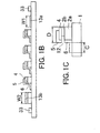
- Figs. 1A to 1C are views schematically illustrating a configuration of the electron emitting device of one pixel arranged on the rear plate of the image display apparatus according to the invention.
- Fig. 1A is a schematic plane view of the electron emitting device
- Fig. 1B is a schematic sectional view of an A-A' section of Fig. 1A
- Fig. 1C is a schematic sectional view illustrating a combination structure of a cathode and a gate constituting one electron emitting part of Fig. 1B .
- reference numerals 2a and 2b denote insulating layers
- 4 denotes a gate
- 5 denotes a gate projecting portion
- 6 denotes a cathode
- 12 denotes an electron emitting part
- 13a and 13b denote electron beam control electrodes
- the same components as those of Fig. 3 are denoted by the same reference numerals.
- the electron emitting device includes the gate 4 and the cathode 6 arranged on a substrate.
- the cathode 6 is connected to a scan wiring 32, and a cathode potential is applied to the cathode 6.
- the gate 4 is connected to a modulation wiring 33, and a gate potential is applied the gate 4.
- any of the cathode 6 and the gate 4 is formed in a comb-teeth shape, and the cathode 6 and the gate 4 are arranged so that the comb-teeth are located alternately in the X-direction.
- each of the comb-shaped teeth of the cathode 6 is formed to have a portion projecting in confrontation with the gate 4.
- the example has the projecting portions located at four positions, the number of the portions is not limited thereto.
- the gate 4 has a projecting portion 5 to correspond to the projecting portion of the cathode 6 so that it confronts the gate 4. Note that the projecting portion 5 is substantially a part of the gate 4.
- the projecting portion 5 of the gate 4 and the projecting portions of the cathode 6 constitute the electron emitting part 12 by confronting one another.
- plural electron emitting parts 12 each including the gate 4 and the cathode 6 confronting each other in one pixel are arranged together in one direction (in the X-direction in the example) parallel to a surface of the substrate.
- all the arrangement directions of the gates 4 and the cathodes 6 positioned between adjacent electron emitting parts are the same in the X-direction.
- electron beam control electrodes are arranged on the external side of an electron emitting part 12 positioned to at least one of outermost portions in the X-direction.
- an electron beam control electrode 13a is arranged on the external side of an electron emitting part 12 at a right end
- an electron beam control electrode 13b is arranged on the external side of an electron emitting part 12 at a left end, respectively.
- Fig. 2 is a view illustrating orbits until electrons emitted from the electron emitting part 12 illustrated in Fig. 1 reach an anode 7.
- the electrons emitted from the electron emitting part 12 are deflected by the gate 4 in the X-direction (corresponding to "deflection direction" of the example). Further, the electrons emitted from the electron emitting part 12 are affected by a peripheral electric field and reach the anode 7 while being diffused.
- Fig. 4A is schematic plan view illustrating the same pixel configuration as that of Fig. 1 except that the electron beam control electrodes 13a and 13b do not exist.
- electron emitting parts 12 positioned on an outermost side adjacent electron emitting parts 12 exist only on one side in the X-direction.
- a disposition of peripheral electrodes is different from that of a central portion, and a periodic property of a peripheral electric field is collapsed as illustrated in Fig. 4B .
- reference numeral 14 in the figure denotes an equipotential line.
- a beam profile an emission current distribution in the X-direction
- a deflection direction of electrons emitted from the electron emitting parts is as illustrated in Fig. 4C .
- a diffusion of the electrons emitted from an electron emitting device cannot be suppressed.
- Fig. 4D is a schematic plan view illustrating a pixel configuration in which the electron beam control electrode 13a is arranged on only the external side of the electron emitting parts 12 at a right end.
- a periodic property of a peripheral electric field of the electron emitting parts 12 is collapsed only on the side (left side) where the control electrode 13a is not arranged as illustrated in Fig. 4E and thus a beam profile to a deflection direction of the electrons emitted from the electron emitting parts 12 is as illustrated in Fig. 4F . Accordingly, a configuration is improved as compared with that of Fig. 4A .
- Fig. 4G is a schematic plan view illustrating a configuration in which the electron beam control electrodes 13a and 13b are arranged at both the ends of the X-direction, and the configuration corresponds to the configuration of Fig. 1A .
- a periodic property of an electric field in a central portion in the X-direction is kept up to the electron emitting parts 12 of both the ends as illustrated in Fig. 4H , and orbits of the electrons emitted from respective electron emitting parts 12 are made uniform.
- a beam profile to a deflection direction is as illustrated in Fig. 4I , and a diffusion of the electrons emitted from the electron emitting parts 12 can be sufficiently suppressed.
- the electron beam control electrode 13a which is arranged on the external side of the gate 4, is connected to the cathode 6 and set to a cathode potential
- the electron beam control electrode 13b which is arranged on the external side of the cathode 6, is connected the gate 4 and set to a gate potential.
- the configuration is a preferable configuration to control potentials of the electron beam control electrodes 13a and 13b, the invention is not limited thereto.
- the periodic property of the electric field of the central portion is kept up to a periphery of the electron emitting part 12 on the outermost side and that orbits of electrons are made uniform, and potentials of the control electrodes 13a and 13b may be separately controlled in a range in which the effect can be obtained.
- the substrate 1 is an insulating substrate for mechanically support a device.
- a quartz glass, a glass in which a content of impurities such as Na is reduced, a blue sheet glass, and a silicon substrate may be used as the substrate 1.
- a function necessary for the substrate 1 is a resistance property to dry etching, wet etching, and alkaline and acid of a developer and the like and in addition to that it has a high mechanical strength.
- the substrate 1 when the substrate 1 is used as an integrated member such as a display panel, it is preferable that the substrate 1 has a small thermal expansion difference between it and a film forming material and other laminating material.
- the substrate is desirably a material in which an alkaline element and the like are unlike to be diffused from the inside of a glass in a heat treatment.
- insulating layers 51, 52 and a conductive layer 53 are sequentially laminated on the substrate 1.
- the insulating layer 51 is an insulating film including a material excellent in a processing property and, for example, SiN (Si x N y ) and SiO 2 and formed by an ordinary vacuum film forming method such as sputtering and the like, a CVD method, and a vacuum vapor deposition method.
- the insulating layer 52 is formed on the insulating layer 51 by the CVD, the vacuum vapor deposition method, and the ordinary vacuum film forming method such as the sputtering and the like.
- a thickness of the insulating layers 51 and 52 is set in a range of 5 nm to 50 ⁇ m and is preferably selected in a range of 50 nm to 500 nm.
- a material having a different etching speed in etching is preferably selected as the insulating layers 51 and 52.
- the insulating layers 51 and 52 preferably have a selection ratio of 10 or more and more preferably have a selection ratio of 50 or more therebetween.
- Si x N y may be used for the insulating layer 51 and an insulating material such as SiO 2 may be used for the insulating layer 52 or a PSG film having a high phosphorus concentration, a BSG film having a high boron concentration, and the like may be used for the insulating layer 52.
- the conductive layer 53 acts as the gate 4 of Fig. 1 and is formed by the ordinary vacuum film forming technique such as the vapor deposition method, the sputtering.
- a material having a high thermal conductivity and a high melting point in addition to a conductive property is preferable as the conductive layer 53.
- metals or alloy materials such as Be, Mg, Ti, Zr, Hf, V, Nb, Ta, Mo, W, Al, Cu, Ni, Cr, Au, Pt, Pd, and the like and carbides such as TiC, ZrC, HfC, TaC, SiC, WC, and the like are exemplified.
- borides of HfB 2 , ZrB 2 , CeB 6 , YB 4 , GdB 4 , and the like, nitrides of TiN, ZrN, HfN, TaN, and the like, semiconductors of Si, Ge, and the like, and organic polymer materials are also exemplified.
- amorphous carbons, graphites, diamond-like carbons, and carbons, carbon compounds, and the like to which diamonds are dispersed are also exemplified, and the material of the conductive layer 53 is appropriately selected therefrom.
- a thickness of the conductive layer 53 is set to a range of 5 nm to 500 nm and is preferably selected in a range of 20 nm to 500 nm.
- the conductive layer 53, the insulating layer 52, and the insulating layer 51 are sequentially processed using an etching method.
- the gate 4, the insulating layer 2b, the insulating layer 2a, and the electron beam control electrode 13b can be obtained.
- RIE Reactive Ion Etching
- a fluorine gas such as CF 4 , CHF 3 , and SF 6 may be selected as a processing gas at the time.
- a chloride gas such as Cl 2 , BCl 3 is selected. Further, to obtain a selection ratio to a resist, hydrogen, oxygen, an argon gas, and the like are added when it is necessary to secure flatness of an etched surface or to increase an etching speed. The etching process may be stopped on an upper surface of the substrate 1, or a part of the substrate 1 may be etched.
- the number n of the gates 4 arranged in the X-direction and a length D of each gate 4 in the X-direction, and an interval S between each gate 4 and an adjacent device may be appropriately changed.
- D is preferably in a range from 5 ⁇ m to 50 ⁇ m. Further, as described above, it is preferable to set W2 ⁇ D.
- a side surface of the insulating layer 2a is partially removed on one side surface of a laminated body including the insulating layers 2a and 2b and the gates 4 using the etching method, and a concave portion 8 is formed.
- the etching method when, for example, the insulating layer 2b is a material including SiO 2 , a mixed solution of ammonium fluoride ordinarily called buffer fluoride acid (BHF) and hydrofluoric acid may be used. Further, when the insulating layer 2b is a material including Si x N y , the etching can be performed by a thermal phosphorus acid etching solution.
- a depth of the concave portion 8, that is, a distance between a side surface of the insulating layer 2b and a side surface of the insulating layer 2a in the concave portion 8 is preferably formed in about 10 nm to 200 nm.
- the invention is by no means limited thereto, and the concave portion 8 may be formed by removing a part of one insulating layer.
- a conductive material is deposited on the substrate 1 and on a side surface of the insulating material 2a. At the time, the conductive material is deposited also on the gate 4. Further, with this configuration, the projecting portion 5, the cathode 6, and the electron beam control electrode 13a can be obtained.
- the conductive material any material may be used as long as it has conductivity and emits electrons to an electric field.
- the conductive material is preferably a material which has a high melting point of 2000°C or higher and a job function of 5 eV or lower and is unlike to form a chemical reaction layer such as oxides or can simply remove a reaction layer.
- Exemplified as the material are for example, metals or alloys such as Hf, V, Nb, Ta, Mo, W, Au, Pt, Pd, carbides such as TiC, ZrC, HfC, TaC, SiC, WC, and borides such as HfB 2 , ZrB 2 , CeB 6 , YB 4 , GdB 4 . Further, exemplified as the material are nitrides such as TiN, ZrN, HfN, TaN and carbons and carbon compounds in which amorphous carbon, graphite, diamond-like carbon and diamonds are dispersed.
- the ordinary vacuum film forming technique such as the vapor deposition method and the sputtering method are used, and an EB vapor deposition method is preferably used.
- a length C of the cathode 6 in the X-direction may be appropriately changed.
- a length D is preferably in a range from 5 ⁇ m to 50 ⁇ m. Further, the length D is preferably set to W1 ⁇ C as described above.
- a structure of the electron emitting device, which can be applied to the invention, is not limited to the mode described here. Any electron emitting device, which has plural gates for deflecting electrons emitted from plural electron emitting parts in the same direction asymmetrically, can be applied to the invention.
- As a configuration of the electron emitting part any arbitrary configuration of a lateral electric field emission device of Spindt-type, a Metal-Insulator-Metal emitting device (MIM-type device ), a surface conductive device (surface conductive emitting device), and the like may be employed.
- a blue sheet glass was used as a substrate 1, and after the substrate 1 was sufficiently rinsed, a Si 3 N 4 film having a thickness of 300 nm was deposited as an insulating layer 51 by sputtering, and next, a SiO 2 film having a thickness of 20 nm was deposited as an insulating layer 52 by sputtering. Thereafter, TaN of 30 nm was deposited as a conductive layer 53 [ Fig. 5A ].
- a positive photoresist was spin-coated, a photo mask pattern was exposed and developed, and a resist pattern was formed.
- the conductive layer 53, the insulating layer 52, and the insulating layer 51 were dry-etched using CF 4 gas and the patterned photoresist as a mask. The dry etching was stopped on the substrate 1, and a laminated body including insulating layers 2a and 2b, and a gate 4 or an electron beam control electrode 13b was formed [ Fig. 5B ].
- the thus formed laminated body was etched for 11 minutes using buffer-fluorinated (BHF) acid (LAL100 made by Stera Chemifa Corporation) as an etching solution, and the insulating layer 2b was selectively etched.
- BHF buffer-fluorinated acid
- a concave portion 8 was formed by etching the insulating layer 2b about 60 nm from a side surface of the laminated body [ Fig. 5C ].
- Mo having a thickness of 30 nm was selectively deposited as a projecting portion 5, a cathode 6, and an electron beam control electrode 13a by oblique deposition from an oblique direction of 45°.
- An electron emitting device was made similarly to the example 1 except that the electron beam control electrode 13b was not formed at step 2.
- An electron emitting device was made similarly to the example 1 except that the electron beam control electrode 13b was not formed at step 2 and further even the electron beam control electrode 13a was not formed at step 4.
- An image display apparatus was made using each of the substrates to which the respective electron emitting devices of the examples 1, 2 and the comparative example 1 were formed as a rear plate and disposing the face plate illustrated in Fig. 3 at a position which is away from the rear plate by 1.6 mm, and the image display apparatus was driven by setting an anode voltage to 12 kV.
- a beam width in the example 1 was 116 ⁇ m
- a beam width in the example 2 was 130 ⁇ m
- a beam width in the comparative example 1 was 180 ⁇ m in a deflection direction (the X-direction) on the face plate, respectively. Accordingly, it has been found that diffusion of electrons can be suppressed by arranging the electron beam control electrode on at least one side or preferably on both the sides.
- an image display apparatus having a plurality of electron emitting parts 12, in which a gate 4 and a cathode 6 are arranged in confrontation with each other, in an X-direction, electron beam control electrodes 13a and 13b are arranged, respectively on the external side of an electron emitting part 12 positioned at an end in the X-direction end portion, the electron beam control electrode 13a having the gate 4 arranged between it and the electron emitting parts 12 is connected to the cathode, and the electron beam control electrode 13b having the cathode 6 between it and the electron emitting parts 12 is connected to the gate 4, respectively.
Landscapes
- Cathode-Ray Tubes And Fluorescent Screens For Display (AREA)
- Electrodes For Cathode-Ray Tubes (AREA)
Abstract
In an image display apparatus having a plurality of electron emitting parts 12, in which a gate 4 and a cathode 6 are arranged in confrontation with each other, in an X-direction, electron beam control electrodes 13a and 13b are arranged, respectively on the external side of an electron emitting part 12 positioned at an end in the X-direction end portion, the electron beam control electrode 13a having the gate 4 arranged between it and the electron emitting parts 12 is connected to the cathode, and the electron beam control electrode 13b having the cathode 6 between it and the electron emitting parts 12 is connected to the gate 4, respectively.
Description
- The invention relates to an image display apparatus including an electron emitting device used for a flat panel display.
- Conventionally, there is known an electron emitting device in which a cathode and a gate are arranged in confrontation with each other and a confronting portion of the cathode and the gate is used as an electron emitting part. Then, an image is displayed by arranging an anode in a portion extending in an emitting direction of electrons emitted from the electron emitting device to accelerate the emitted electrons, further arranging a light emitting member behind the anode, and emitting the light emitting member by colliding electrons to the anode.
- Japanese Patent Application Laid-Open No.
2001-167693 - The present invention provides an image display apparatus excellent in display quality by making orbits of electron beams uniform in pixels in an electron emitting device having plural electron emitting parts in one pixel.
- The present invention in its first aspect provides an image display apparatus as specified in
claims 1 to 5. - In the invention, in a configuration in which plural electron emitting parts are arranged in one direction and gates and cathodes are arranged in the same direction between adjacent electron emitting parts, since an electron beam control electrode is arranged on the external side of an electron emitting part at an end, orbits of electron beams can be made uniform. Accordingly, an image display apparatus of the invention can display an excellent image having a uniform distribution of brightness.
- Further features of the present invention will become apparent from the following description of exemplary embodiments with reference to the attached drawings.
-
-
Fig. 1A is a schematic plan view of one pixel of an image display apparatus of the invention,Fig. 1B is a schematic sectional view of the one pixel, andFig. 1C is a schematic sectional view of one electron emitting part. -
Fig. 2 is a view illustrating orbits of electron beams of the electron emitting device according to the invention. -
Fig. 3 is a view schematically illustrating a configuration of the image display apparatus of the invention. -
Figs. 4A to 4I are explanatory views of operations of an electron beam control electrode according to the invention. -
Figs. 5A to 5D are views illustrating manufacturing steps of the electron emitting device in an embodiment of the invention. - A configuration of an image display apparatus of the invention will be described using
Fig. 3. Fig. 3 is a perspective view schematically illustrating a configuration example of a display panel of the image display apparatus according to the invention, wherein the perspective view is partially cut out to show an internal structure of the display panel. In the view,reference numeral 1 denotes a substrate, 32 denotes a scan wiring, 33 denotes a modulation wiring, and 34 denotes an electron emitting device.Reference numeral 41 denotes a rear plate on which the substrate (first substrate) 1 is fixed, 46 denotes a face plate in which aphosphor 44 as a light emitting member, ametal back 45 as an anode, and the like are formed on an inner surface of a glass substrate (second substrate) 43.Reference numeral 42 denotes a support frame, and anexternal enclosure 47 is configured by attaching therear plate 41 and theface plate 46 to thesupport frame 42 through a flit glass and the like. Since therear plate 41 is arranged for purposes of mainly reinforcing the strength of thesubstrate 1, when thesubstrate 1 has a sufficient strength by itself, therear plate 41 as a separate member is not necessary. Further, a configuration having a sufficient strength to atmospheric pressure can be also provided by interposing a not illustrated support member called a spacer between theface plate 46 and therear plate 41. - M pieces of
scan wirings 32 are connected to terminals Dx1, Dx2, ..., Dxm. N pieces ofmodulation wirings 33 are connected to terminals Dy1, Dy2, ..., Dyn (m and n are positive integers). Not illustrated interlayer insulating layers are arranged between the m pieces of thescan wirings 32 and the n pieces of themodulation wirings 33 to electrically separate them from one another. A high voltage terminal is connected to ametal back 45, and a direct current voltage of 10 [kV], for example, is supplied to themetal back 45. The voltage is an acceleration voltage for applying a sufficient energy for exciting a phosphor to electrons emitted from the electron emitting device. - The rear plate according to the invention has the plural
electron emitting devices 34 connected in a matrix state by thescan wirings 32 and themodulation wirings 33. A scan circuit (not illustrated) is connected to thescan wirings 32 to apply a scan signal for selecting a row of theelectron emitting devices 34 arranged in an X-direction. In contrast, a modulation circuit (not illustrated) is connected to themodulation wirings 33 to modulate respective columns of theelectron emitting device 34 arranged in a Y-direction in response to an input signal. A drive voltage applied to the respective electron emitting devices is supplied as a difference voltage between a scan signal and a modulation signal applied to the electron emitting devices. The drive voltage is preferably in a range of 10 V to 100 V and more preferable in a range of 10 V to 30 V. -
Figs. 1A to 1C are views schematically illustrating a configuration of the electron emitting device of one pixel arranged on the rear plate of the image display apparatus according to the invention.
Fig. 1A is a schematic plane view of the electron emitting device,Fig. 1B is a schematic sectional view of an A-A' section ofFig. 1A , andFig. 1C is a schematic sectional view illustrating a combination structure of a cathode and a gate constituting one electron emitting part ofFig. 1B . In the figures,reference numerals Fig. 3 are denoted by the same reference numerals. - The electron emitting device according to the invention includes the
gate 4 and thecathode 6 arranged on a substrate. In the example, thecathode 6 is connected to ascan wiring 32, and a cathode potential is applied to thecathode 6. Further, thegate 4 is connected to amodulation wiring 33, and a gate potential is applied thegate 4. In the example, any of thecathode 6 and thegate 4 is formed in a comb-teeth shape, and thecathode 6 and thegate 4 are arranged so that the comb-teeth are located alternately in the X-direction. Further, each of the comb-shaped teeth of thecathode 6 is formed to have a portion projecting in confrontation with thegate 4. Although the example has the projecting portions located at four positions, the number of the portions is not limited thereto. Further, thegate 4 has a projectingportion 5 to correspond to the projecting portion of thecathode 6 so that it confronts thegate 4. Note that the projectingportion 5 is substantially a part of thegate 4. In the invention, the projectingportion 5 of thegate 4 and the projecting portions of thecathode 6 constitute theelectron emitting part 12 by confronting one another. - As illustrated in
Fig. 1 , in the invention, pluralelectron emitting parts 12 each including thegate 4 and thecathode 6 confronting each other in one pixel are arranged together in one direction (in the X-direction in the example) parallel to a surface of the substrate. In the parallel configuration, as illustrated inFig. 1 , all the arrangement directions of thegates 4 and thecathodes 6 positioned between adjacent electron emitting parts are the same in the X-direction. - In the above configuration of the invention, electron beam control electrodes are arranged on the external side of an
electron emitting part 12 positioned to at least one of outermost portions in the X-direction. In the example, an electronbeam control electrode 13a is arranged on the external side of anelectron emitting part 12 at a right end, and an electronbeam control electrode 13b is arranged on the external side of anelectron emitting part 12 at a left end, respectively. - An operation of the electron
beam control electrodes Figs. 2 and4 . -
Fig. 2 is a view illustrating orbits until electrons emitted from theelectron emitting part 12 illustrated inFig. 1 reach ananode 7. The electrons emitted from theelectron emitting part 12 are deflected by thegate 4 in the X-direction (corresponding to "deflection direction" of the example). Further, the electrons emitted from theelectron emitting part 12 are affected by a peripheral electric field and reach theanode 7 while being diffused. -
Fig. 4A is schematic plan view illustrating the same pixel configuration as that ofFig. 1 except that the electronbeam control electrodes electron emitting parts 12 positioned on an outermost side, adjacentelectron emitting parts 12 exist only on one side in the X-direction. Thus, a disposition of peripheral electrodes is different from that of a central portion, and a periodic property of a peripheral electric field is collapsed as illustrated inFig. 4B . Incidentally,reference numeral 14 in the figure denotes an equipotential line. Accordingly, a beam profile (an emission current distribution in the X-direction) to a deflection direction of electrons emitted from the electron emitting parts is as illustrated inFig. 4C . Thus, in this case, a diffusion of the electrons emitted from an electron emitting device cannot be suppressed. -
Fig. 4D is a schematic plan view illustrating a pixel configuration in which the electronbeam control electrode 13a is arranged on only the external side of theelectron emitting parts 12 at a right end. In this case, a periodic property of a peripheral electric field of theelectron emitting parts 12 is collapsed only on the side (left side) where thecontrol electrode 13a is not arranged as illustrated inFig. 4E and thus a beam profile to a deflection direction of the electrons emitted from theelectron emitting parts 12 is as illustrated inFig. 4F . Accordingly, a configuration is improved as compared with that ofFig. 4A . -
Fig. 4G is a schematic plan view illustrating a configuration in which the electronbeam control electrodes Fig. 1A . In the configuration, a periodic property of an electric field in a central portion in the X-direction is kept up to theelectron emitting parts 12 of both the ends as illustrated inFig. 4H , and orbits of the electrons emitted from respectiveelectron emitting parts 12 are made uniform. Thus, a beam profile to a deflection direction is as illustrated inFig. 4I , and a diffusion of the electrons emitted from theelectron emitting parts 12 can be sufficiently suppressed. - In the invention, to sufficiently exhibit an effect obtained from a width W1 of the electron
beam control electrode 13a and from a width W2 of the electronbeam control electrode 13b in the X-direction, it is preferable to satisfy a relation of W1 ≥ C, W2 ≥ D between a width C of thecathode 6 and a width D of thegate 4. - Incidentally, in the example, the electron
beam control electrode 13a, which is arranged on the external side of thegate 4, is connected to thecathode 6 and set to a cathode potential, and the electronbeam control electrode 13b, which is arranged on the external side of thecathode 6, is connected thegate 4 and set to a gate potential. Although the configuration is a preferable configuration to control potentials of the electronbeam control electrodes electron emitting part 12 on the outermost side and that orbits of electrons are made uniform, and potentials of thecontrol electrodes - Next, a method of manufacturing the electron emitting device of the invention will be described by exemplifying a configuration example of
Fig. 1 usingFig. 5 . - The
substrate 1 is an insulating substrate for mechanically support a device. For example, a quartz glass, a glass in which a content of impurities such as Na is reduced, a blue sheet glass, and a silicon substrate may be used as thesubstrate 1. A function necessary for thesubstrate 1 is a resistance property to dry etching, wet etching, and alkaline and acid of a developer and the like and in addition to that it has a high mechanical strength. Further, when thesubstrate 1 is used as an integrated member such as a display panel, it is preferable that thesubstrate 1 has a small thermal expansion difference between it and a film forming material and other laminating material. Further, the substrate is desirably a material in which an alkaline element and the like are unlike to be diffused from the inside of a glass in a heat treatment. - As illustrated in
Fig. 5 , insulatinglayers conductive layer 53 are sequentially laminated on thesubstrate 1. The insulatinglayer 51 is an insulating film including a material excellent in a processing property and, for example, SiN (SixNy) and SiO2 and formed by an ordinary vacuum film forming method such as sputtering and the like, a CVD method, and a vacuum vapor deposition method. Next, the insulatinglayer 52 is formed on the insulatinglayer 51 by the CVD, the vacuum vapor deposition method, and the ordinary vacuum film forming method such as the sputtering and the like. A thickness of the insulatinglayers layers layer 51 and an insulating material such as SiO2 may be used for the insulatinglayer 52 or a PSG film having a high phosphorus concentration, a BSG film having a high boron concentration, and the like may be used for the insulatinglayer 52. - Further, the
conductive layer 53 acts as thegate 4 ofFig. 1 and is formed by the ordinary vacuum film forming technique such as the vapor deposition method, the sputtering. A material having a high thermal conductivity and a high melting point in addition to a conductive property is preferable as theconductive layer 53. For example, metals or alloy materials such as Be, Mg, Ti, Zr, Hf, V, Nb, Ta, Mo, W, Al, Cu, Ni, Cr, Au, Pt, Pd, and the like and carbides such as TiC, ZrC, HfC, TaC, SiC, WC, and the like are exemplified. Further, borides of HfB2, ZrB2, CeB6, YB4, GdB4, and the like, nitrides of TiN, ZrN, HfN, TaN, and the like, semiconductors of Si, Ge, and the like, and organic polymer materials are also exemplified. Further, amorphous carbons, graphites, diamond-like carbons, and carbons, carbon compounds, and the like to which diamonds are dispersed are also exemplified, and the material of theconductive layer 53 is appropriately selected therefrom. A thickness of theconductive layer 53 is set to a range of 5 nm to 500 nm and is preferably selected in a range of 20 nm to 500 nm. - Next, as illustrated in
Fig. 5B , after a resist pattern is formed on theconductive layer 53 by a photolithographic technique, theconductive layer 53, the insulatinglayer 52, and the insulatinglayer 51 are sequentially processed using an etching method. With this configuration, thegate 4, the insulatinglayer 2b, the insulatinglayer 2a, and the electronbeam control electrode 13b can be obtained. In the etching process, Reactive Ion Etching (RIE), which can etch a material precisely by ordinarily making an etching gas to plasma and radiating it to the material. When a target member to be processed creates fluorides, a fluorine gas such as CF4, CHF3, and SF6 may be selected as a processing gas at the time. Further, when chlorides are formed as in Si and Al, a chloride gas such as Cl2, BCl3 is selected. Further, to obtain a selection ratio to a resist, hydrogen, oxygen, an argon gas, and the like are added when it is necessary to secure flatness of an etched surface or to increase an etching speed. The etching process may be stopped on an upper surface of thesubstrate 1, or a part of thesubstrate 1 may be etched. - Incidentally, the number n of the
gates 4 arranged in the X-direction and a length D of eachgate 4 in the X-direction, and an interval S between eachgate 4 and an adjacent device may be appropriately changed. D is preferably in a range from 5 µm to 50 µm. Further, as described above, it is preferable to set W2 ≥ D. - Next, as illustrated in
Fig. 5C , only a side surface of the insulatinglayer 2a is partially removed on one side surface of a laminated body including the insulatinglayers gates 4 using the etching method, and aconcave portion 8 is formed. In the etching method, when, for example, the insulatinglayer 2b is a material including SiO2, a mixed solution of ammonium fluoride ordinarily called buffer fluoride acid (BHF) and hydrofluoric acid may be used. Further, when the insulatinglayer 2b is a material including SixNy, the etching can be performed by a thermal phosphorus acid etching solution. A depth of theconcave portion 8, that is, a distance between a side surface of the insulatinglayer 2b and a side surface of the insulatinglayer 2a in theconcave portion 8 is preferably formed in about 10 nm to 200 nm. - In the example, although a mode in which the insulating
layers concave portion 8 may be formed by removing a part of one insulating layer. - Next, as illustrated in
Fig. 5D , a conductive material is deposited on thesubstrate 1 and on a side surface of the insulatingmaterial 2a. At the time, the conductive material is deposited also on thegate 4. Further, with this configuration, the projectingportion 5, thecathode 6, and the electronbeam control electrode 13a can be obtained. As the conductive material, any material may be used as long as it has conductivity and emits electrons to an electric field. The conductive material is preferably a material which has a high melting point of 2000°C or higher and a job function of 5 eV or lower and is unlike to form a chemical reaction layer such as oxides or can simply remove a reaction layer. Exemplified as the material are for example, metals or alloys such as Hf, V, Nb, Ta, Mo, W, Au, Pt, Pd, carbides such as TiC, ZrC, HfC, TaC, SiC, WC, and borides such as HfB2, ZrB2, CeB6, YB4, GdB4. Further, exemplified as the material are nitrides such as TiN, ZrN, HfN, TaN and carbons and carbon compounds in which amorphous carbon, graphite, diamond-like carbon and diamonds are dispersed. As a deposition method of the conductive material, the ordinary vacuum film forming technique such as the vapor deposition method and the sputtering method are used, and an EB vapor deposition method is preferably used. - A length C of the
cathode 6 in the X-direction may be appropriately changed. A length D is preferably in a range from 5 µm to 50 µm. Further, the length D is preferably set to W1 ≥ C as described above. - A structure of the electron emitting device, which can be applied to the invention, is not limited to the mode described here. Any electron emitting device, which has plural gates for deflecting electrons emitted from plural electron emitting parts in the same direction asymmetrically, can be applied to the invention. As a configuration of the electron emitting part, any arbitrary configuration of a lateral electric field emission device of Spindt-type, a Metal-Insulator-Metal emitting device (MIM-type device ), a surface conductive device (surface conductive emitting device), and the like may be employed.
- An electron emitting device having the configuration illustrated in
Fig. 1 was made according to steps ofFig. 5 . The respective steps will be described below. - A blue sheet glass was used as a
substrate 1, and after thesubstrate 1 was sufficiently rinsed, a Si3N4 film having a thickness of 300 nm was deposited as an insulatinglayer 51 by sputtering, and next, a SiO2 film having a thickness of 20 nm was deposited as an insulatinglayer 52 by sputtering. Thereafter, TaN of 30 nm was deposited as a conductive layer 53 [Fig. 5A ]. - Next, a positive photoresist was spin-coated, a photo mask pattern was exposed and developed, and a resist pattern was formed. At the time, the resist pattern was formed so that it was set to D = 10 µm, S = 12 µm, and W2 = 20 µm. Thereafter, the
conductive layer 53, the insulatinglayer 52, and the insulatinglayer 51 were dry-etched using CF4 gas and the patterned photoresist as a mask. The dry etching was stopped on thesubstrate 1, and a laminated body including insulatinglayers gate 4 or an electronbeam control electrode 13b was formed [Fig. 5B ]. - Next, the thus formed laminated body was etched for 11 minutes using buffer-fluorinated (BHF) acid (LAL100 made by Stera Chemifa Corporation) as an etching solution, and the insulating
layer 2b was selectively etched. Aconcave portion 8 was formed by etching the insulatinglayer 2b about 60 nm from a side surface of the laminated body [Fig. 5C ]. - Next, Mo having a thickness of 30 nm was selectively deposited as a projecting
portion 5, acathode 6, and an electronbeam control electrode 13a by oblique deposition from an oblique direction of 45°. At the time, a resist pattern was formed so that it was set to C = 10 µm, W1 = 20 µm [Fig. 5D ]. - An electron emitting device was made similarly to the example 1 except that the electron
beam control electrode 13b was not formed atstep 2. - An electron emitting device was made similarly to the example 1 except that the electron
beam control electrode 13b was not formed atstep 2 and further even the electronbeam control electrode 13a was not formed atstep 4. - An image display apparatus was made using each of the substrates to which the respective electron emitting devices of the examples 1, 2 and the comparative example 1 were formed as a rear plate and disposing the face plate illustrated in
Fig. 3 at a position which is away from the rear plate by 1.6 mm, and the image display apparatus was driven by setting an anode voltage to 12 kV. As a result, a beam width in the example 1 was 116 µm, a beam width in the example 2 was 130 µm, and a beam width in the comparative example 1 was 180 µm in a deflection direction (the X-direction) on the face plate, respectively. Accordingly, it has been found that diffusion of electrons can be suppressed by arranging the electron beam control electrode on at least one side or preferably on both the sides. - While the present invention has been described with reference to exemplary embodiments, it is to be understood that the invention is not limited to the disclosed exemplary embodiments. The scope of the following claims is to be accorded the broadest interpretation so as to encompass all such modifications and equivalent structures and functions.
In an image display apparatus having a plurality ofelectron emitting parts 12, in which agate 4 and acathode 6 are arranged in confrontation with each other, in an X-direction, electronbeam control electrodes electron emitting part 12 positioned at an end in the X-direction end portion, the electronbeam control electrode 13a having thegate 4 arranged between it and theelectron emitting parts 12 is connected to the cathode, and the electronbeam control electrode 13b having thecathode 6 between it and theelectron emitting parts 12 is connected to thegate 4, respectively.
Claims (5)
- An image display apparatus comprising
a rear plate having a first substrate, a gate (4) and a cathode (6) arranged on the substrate and a plurality of electron emitting devices which arrange a portion where the cathode confronts with the gate as an electron emitting part (12), and
a face plate having a second substrate, an anode (7) arranged in confrontation with the electron emitting device of the rear plate and accelerating electrons emitted from the electron emitting device and a light emitting member which emits light by irradiation of the electrons,
wherein the plurality of electron emitting devices have a plurality of electron emitting parts in one direction parallel to a surface of the first substrate, and the gate and the cathode are arranged together in the same arrangement direction between the electron emitting parts adjacent in the one direction; and
an electron beam control electrode (13) is arranged on the external side of an electron emitting part positioned in at least one of the outermost portions of the respective electron emitting devices in the one direction. - An image display apparatus according to claim 1, wherein
the electron beam control electrode is connected to the cathode, and
the gate is positioned between the electron emitting parts positioned in the outermost portion and the electron beam control electrode. - An image display apparatus according to claim 2, wherein
a width C of a cathode in the one direction and a width W1 of the electron beam control electrode satisfy a relation of W1 ≥ C. - An image display apparatus according to any one of claims 1 to 3, wherein
the electron beam control electrode is connected to a gate,
a cathode is positioned between the electron emitting parts positioned in the outermost portions and the electron beam control electrode. - An image display apparatus according to claim 4, wherein
a width D of a gate in the one direction and a width W2 of the electron beam control electrode satisfy a relation of W2 ≥ D.
Applications Claiming Priority (1)
| Application Number | Priority Date | Filing Date | Title |
|---|---|---|---|
| JP2009098833A JP2010251102A (en) | 2009-04-15 | 2009-04-15 | Image display device |
Publications (1)
| Publication Number | Publication Date |
|---|---|
| EP2242083A1 true EP2242083A1 (en) | 2010-10-20 |
Family
ID=42320726
Family Applications (1)
| Application Number | Title | Priority Date | Filing Date |
|---|---|---|---|
| EP10156486A Withdrawn EP2242083A1 (en) | 2009-04-15 | 2010-03-15 | Electron beam device |
Country Status (4)
| Country | Link |
|---|---|
| US (1) | US20100264808A1 (en) |
| EP (1) | EP2242083A1 (en) |
| JP (1) | JP2010251102A (en) |
| CN (1) | CN101866800A (en) |
Cited By (1)
| Publication number | Priority date | Publication date | Assignee | Title |
|---|---|---|---|---|
| EP2267748A3 (en) * | 2009-06-23 | 2011-09-21 | Canon Kabushiki Kaisha | Image display apparatus |
Citations (9)
| Publication number | Priority date | Publication date | Assignee | Title |
|---|---|---|---|---|
| JP2001167693A (en) | 1999-12-08 | 2001-06-22 | Canon Inc | Electron emitting device, electron source, image forming apparatus, and method of manufacturing electron emitting device |
| US20020135284A1 (en) * | 2001-03-20 | 2002-09-26 | Alexander Kastalsky | Field-emission matrix display based on lateral electron reflections |
| EP1347487A2 (en) * | 1998-12-08 | 2003-09-24 | Canon Kabushiki Kaisha | Electron-emitting device, electron source using the electron-emitting devices, and image-forming apparatus using the electron source |
| US20040000861A1 (en) * | 2002-06-26 | 2004-01-01 | Dorfman Benjamin F. | Carbon-metal nano-composite materials for field emission cathodes and devices |
| US20080150415A1 (en) * | 2006-12-22 | 2008-06-26 | Masato Kaneeda | Image Display Device and Process of Manufacture |
| EP2109131A2 (en) * | 2008-04-10 | 2009-10-14 | Canon Kabushiki Kaisha | Electron beam apparatus and image display apparatus using the same |
| EP2109132A2 (en) * | 2008-04-10 | 2009-10-14 | Canon Kabushiki Kaisha | Electron beam apparatus and image display apparatus using the same |
| EP2113934A2 (en) * | 2008-05-02 | 2009-11-04 | Canon Kabushiki Kaisha | Electron source and image display apparatus |
| EP2161734A2 (en) * | 2008-09-03 | 2010-03-10 | Canon Kabushiki Kaisha | Electron emission device and image display panel using the same, and image display apparatus and information display apparatus |
Family Cites Families (4)
| Publication number | Priority date | Publication date | Assignee | Title |
|---|---|---|---|---|
| US6005333A (en) * | 1993-05-05 | 1999-12-21 | Canon Kabushiki Kaisha | Electron beam-generating device, and image-forming apparatus and recording apparatus employing the same |
| WO2003032334A1 (en) * | 2001-09-10 | 2003-04-17 | Noritake Co., Limited | Thick-film sheet member, its applied device, and methods for manufacturing them |
| JP4806968B2 (en) * | 2005-05-30 | 2011-11-02 | ソニー株式会社 | Cold cathode field emission display |
| JP2009302003A (en) * | 2008-06-17 | 2009-12-24 | Canon Inc | Electron emitting element and image display device |
-
2009
- 2009-04-15 JP JP2009098833A patent/JP2010251102A/en not_active Withdrawn
-
2010
- 2010-03-11 US US12/722,274 patent/US20100264808A1/en not_active Abandoned
- 2010-03-15 EP EP10156486A patent/EP2242083A1/en not_active Withdrawn
- 2010-04-12 CN CN201010164044A patent/CN101866800A/en active Pending
Patent Citations (10)
| Publication number | Priority date | Publication date | Assignee | Title |
|---|---|---|---|---|
| EP1347487A2 (en) * | 1998-12-08 | 2003-09-24 | Canon Kabushiki Kaisha | Electron-emitting device, electron source using the electron-emitting devices, and image-forming apparatus using the electron source |
| JP2001167693A (en) | 1999-12-08 | 2001-06-22 | Canon Inc | Electron emitting device, electron source, image forming apparatus, and method of manufacturing electron emitting device |
| US20020135284A1 (en) * | 2001-03-20 | 2002-09-26 | Alexander Kastalsky | Field-emission matrix display based on lateral electron reflections |
| WO2002086931A1 (en) * | 2001-04-19 | 2002-10-31 | Copytele, Inc. | Field-emission matrix display based on lateral electron reflections |
| US20040000861A1 (en) * | 2002-06-26 | 2004-01-01 | Dorfman Benjamin F. | Carbon-metal nano-composite materials for field emission cathodes and devices |
| US20080150415A1 (en) * | 2006-12-22 | 2008-06-26 | Masato Kaneeda | Image Display Device and Process of Manufacture |
| EP2109131A2 (en) * | 2008-04-10 | 2009-10-14 | Canon Kabushiki Kaisha | Electron beam apparatus and image display apparatus using the same |
| EP2109132A2 (en) * | 2008-04-10 | 2009-10-14 | Canon Kabushiki Kaisha | Electron beam apparatus and image display apparatus using the same |
| EP2113934A2 (en) * | 2008-05-02 | 2009-11-04 | Canon Kabushiki Kaisha | Electron source and image display apparatus |
| EP2161734A2 (en) * | 2008-09-03 | 2010-03-10 | Canon Kabushiki Kaisha | Electron emission device and image display panel using the same, and image display apparatus and information display apparatus |
Cited By (1)
| Publication number | Priority date | Publication date | Assignee | Title |
|---|---|---|---|---|
| EP2267748A3 (en) * | 2009-06-23 | 2011-09-21 | Canon Kabushiki Kaisha | Image display apparatus |
Also Published As
| Publication number | Publication date |
|---|---|
| CN101866800A (en) | 2010-10-20 |
| JP2010251102A (en) | 2010-11-04 |
| US20100264808A1 (en) | 2010-10-21 |
Similar Documents
| Publication | Publication Date | Title |
|---|---|---|
| JP4380792B2 (en) | Electron beam apparatus, image display apparatus using the same, and electron-emitting device | |
| JP3745348B2 (en) | Electron emitting device, electron source, and manufacturing method of image display device | |
| US7982381B2 (en) | Electron source and image display apparatus | |
| US8075361B2 (en) | Electron source manufacturing method | |
| US7435689B2 (en) | Process for fabricating electron emitting device, electron source, and image display device | |
| US20100060141A1 (en) | Electron beam device and image display apparatus using the same | |
| EP2242083A1 (en) | Electron beam device | |
| US20090309479A1 (en) | Electron emitting-device and image display apparatus | |
| US8093796B2 (en) | Electron beam apparatus and image display apparatus | |
| KR101010987B1 (en) | Electron beam device and image display device using the same | |
| US8035294B2 (en) | Electron beam apparatus and image display apparatus therewith | |
| JP2010182585A (en) | Electron emission element, and image display using the same | |
| EP2239754A1 (en) | Electron beam apparatus and image displaying apparatus | |
| EP2251888A2 (en) | Electron beam apparatus and image display apparatus using the same | |
| EP2267748A2 (en) | Image display apparatus | |
| JP2010186655A (en) | Electron beam device and image display device using the same | |
| JP2010186615A (en) | Electron beam device and image display using this |
Legal Events
| Date | Code | Title | Description |
|---|---|---|---|
| PUAI | Public reference made under article 153(3) epc to a published international application that has entered the european phase |
Free format text: ORIGINAL CODE: 0009012 |
|
| AK | Designated contracting states |
Kind code of ref document: A1 Designated state(s): AT BE BG CH CY CZ DE DK EE ES FI FR GB GR HR HU IE IS IT LI LT LU LV MC MK MT NL NO PL PT RO SE SI SK SM TR |
|
| AX | Request for extension of the european patent |
Extension state: AL BA ME RS |
|
| 17P | Request for examination filed |
Effective date: 20110420 |
|
| STAA | Information on the status of an ep patent application or granted ep patent |
Free format text: STATUS: THE APPLICATION HAS BEEN WITHDRAWN |
|
| 18W | Application withdrawn |
Effective date: 20110727 |