EP2238808B1 - Frequency converted dimming signal generation - Google Patents
Frequency converted dimming signal generation Download PDFInfo
- Publication number
- EP2238808B1 EP2238808B1 EP09704232.9A EP09704232A EP2238808B1 EP 2238808 B1 EP2238808 B1 EP 2238808B1 EP 09704232 A EP09704232 A EP 09704232A EP 2238808 B1 EP2238808 B1 EP 2238808B1
- Authority
- EP
- European Patent Office
- Prior art keywords
- duty cycle
- waveform
- voltage
- input
- output
- Prior art date
- Legal status (The legal status is an assumption and is not a legal conclusion. Google has not performed a legal analysis and makes no representation as to the accuracy of the status listed.)
- Active
Links
- 230000007274 generation of a signal involved in cell-cell signaling Effects 0.000 title 1
- 238000001514 detection method Methods 0.000 claims abstract description 95
- 230000000737 periodic effect Effects 0.000 claims abstract description 13
- 238000012935 Averaging Methods 0.000 claims description 41
- 230000007423 decrease Effects 0.000 claims description 12
- 238000000034 method Methods 0.000 claims description 11
- 239000007787 solid Substances 0.000 claims description 10
- 230000004044 response Effects 0.000 claims description 9
- 238000006243 chemical reaction Methods 0.000 description 30
- 238000010586 diagram Methods 0.000 description 19
- 230000006870 function Effects 0.000 description 7
- 230000008859 change Effects 0.000 description 6
- 230000009467 reduction Effects 0.000 description 5
- 239000003990 capacitor Substances 0.000 description 4
- 230000007704 transition Effects 0.000 description 4
- 230000003247 decreasing effect Effects 0.000 description 3
- 238000009499 grossing Methods 0.000 description 2
- 238000005286 illumination Methods 0.000 description 2
- 230000001105 regulatory effect Effects 0.000 description 2
- 230000003252 repetitive effect Effects 0.000 description 2
- 230000002441 reversible effect Effects 0.000 description 2
- 241000251730 Chondrichthyes Species 0.000 description 1
- 230000009286 beneficial effect Effects 0.000 description 1
- 230000033228 biological regulation Effects 0.000 description 1
- 230000001276 controlling effect Effects 0.000 description 1
- 230000001419 dependent effect Effects 0.000 description 1
- 230000000694 effects Effects 0.000 description 1
- 238000001914 filtration Methods 0.000 description 1
- 235000020130 leben Nutrition 0.000 description 1
- 230000003278 mimic effect Effects 0.000 description 1
- 230000008447 perception Effects 0.000 description 1
- 235000020030 perry Nutrition 0.000 description 1
Images


Classifications
-
- H—ELECTRICITY
- H05—ELECTRIC TECHNIQUES NOT OTHERWISE PROVIDED FOR
- H05B—ELECTRIC HEATING; ELECTRIC LIGHT SOURCES NOT OTHERWISE PROVIDED FOR; CIRCUIT ARRANGEMENTS FOR ELECTRIC LIGHT SOURCES, IN GENERAL
- H05B45/00—Circuit arrangements for operating light-emitting diodes [LED]
- H05B45/30—Driver circuits
- H05B45/31—Phase-control circuits
-
- H—ELECTRICITY
- H05—ELECTRIC TECHNIQUES NOT OTHERWISE PROVIDED FOR
- H05B—ELECTRIC HEATING; ELECTRIC LIGHT SOURCES NOT OTHERWISE PROVIDED FOR; CIRCUIT ARRANGEMENTS FOR ELECTRIC LIGHT SOURCES, IN GENERAL
- H05B39/00—Circuit arrangements or apparatus for operating incandescent light sources
- H05B39/04—Controlling
- H05B39/041—Controlling the light-intensity of the source
- H05B39/044—Controlling the light-intensity of the source continuously
-
- H—ELECTRICITY
- H05—ELECTRIC TECHNIQUES NOT OTHERWISE PROVIDED FOR
- H05B—ELECTRIC HEATING; ELECTRIC LIGHT SOURCES NOT OTHERWISE PROVIDED FOR; CIRCUIT ARRANGEMENTS FOR ELECTRIC LIGHT SOURCES, IN GENERAL
- H05B45/00—Circuit arrangements for operating light-emitting diodes [LED]
- H05B45/10—Controlling the intensity of the light
-
- H—ELECTRICITY
- H05—ELECTRIC TECHNIQUES NOT OTHERWISE PROVIDED FOR
- H05B—ELECTRIC HEATING; ELECTRIC LIGHT SOURCES NOT OTHERWISE PROVIDED FOR; CIRCUIT ARRANGEMENTS FOR ELECTRIC LIGHT SOURCES, IN GENERAL
- H05B45/00—Circuit arrangements for operating light-emitting diodes [LED]
- H05B45/30—Driver circuits
- H05B45/37—Converter circuits
- H05B45/3725—Switched mode power supply [SMPS]
- H05B45/375—Switched mode power supply [SMPS] using buck topology
-
- H—ELECTRICITY
- H05—ELECTRIC TECHNIQUES NOT OTHERWISE PROVIDED FOR
- H05B—ELECTRIC HEATING; ELECTRIC LIGHT SOURCES NOT OTHERWISE PROVIDED FOR; CIRCUIT ARRANGEMENTS FOR ELECTRIC LIGHT SOURCES, IN GENERAL
- H05B45/00—Circuit arrangements for operating light-emitting diodes [LED]
- H05B45/30—Driver circuits
- H05B45/37—Converter circuits
- H05B45/3725—Switched mode power supply [SMPS]
- H05B45/38—Switched mode power supply [SMPS] using boost topology
Definitions
- Patent document US 2003l0146715 A1 discloses lighting control circuits, each of which has a phase angle dimmer that provides a series of lamp operating pulses to a lamp controller circuit.
- the lamp controller circuits each include a buck converter that receives a dimmed and rectified line voltage and which is controlled by a signal that is derived from the dimmed and rectified line voltage. This provides a variable pulse transfer characteristic that provides a steady lamp power even when input power is decreased owing to power drawn by accessories also connected to the phase angle dimmer.
- FIG. 1A An example of a cycle of a full wave rectified AC signal is provided in Fig. 1A , a cycle of a phase cut rectified AC waveform is illustrated in Fig. 1B and a cycle of a reverse phase cut AC waveform is illustrated in Fig. 1C .
- Figs. 1A through 1C when phase cut dimming is utilized, the duty cycle of the resulting rectified waveform is changed. This change in duty cycle, if sufficiently large, is noticeable as a decrease in light output from an incandescent lamp. The "off" time does not result in flickering of the incandescent lamp because the filament of an incandescent lamp has some thermal inertia and will remain at a sufficient temperature to emit light even during the "off" time when no current flows through the filament.
- solid state lighting systems have been developed that provide light for general illumination. These solid state lighting systems utilize light emitting diodes or other solid state light sources that are coupled to a power supply that receives the AC line voltage and converts that voltage to a voltage and/or current suitable for driving the solid state light emitters.
- Typical power supplies for light emitting diode light sources include linear current regulated supplies and/or pulse width modulated current and/or voltage regulated supplies.
- dimming that is based on varying the duty cycle of the line voltage may present several challenges in power supply design for solid state lighting.
- LEDs typically have very rapid response times to changes in current. This rapid response of LEDs may, in combination with conventional dimming circuits, present difficulties in driving LEDs.
- variation in the input signal may affect the ability to detect the presence of a phase cut dimmer or may make detection unreliable. For example, in systems that detect the presence of a phase cut dimmer based on detection of the leading edge of the phase cut AC input, if a reverse-phase cut dimmer is used, the dimming is never detected. Likewise, many residential dimmers have substantial variation in pulse width even without changing the setting of a dimmer. If a power supply detects the presence of dimming based on a threshold pulse width, the power supply could detect the presence of dimming on one cycle and not on another as a result of this the variation in pulse width.
- the various aspects of the present inventive subject matter include various combinations of electronic components (transformers, switches; diodes, capacitors, transistors, etc.). Persons skilled in the art are familiar with and have access to a wide variety of such components, and any of such components can be used in making the devices according to the present inventive subject matter. In addition, persons skilled in the art are able to select suitable components from among the various choices based on requirements of the loads and the selection of other components in the circuitry. Any of the circuits described herein (and/or any portions of such circuits) can be provided in the form of (1) one or more discrete components, (2) one or more integrated circuits, or (3) combinations of one or more discrete components and one or more integrated circuits.
- two components in a device are "electrically connected,” means that there are no components electrically between the components that materially affect the function or functions provided by the device.
- two components can be referred to as being electrically connected, even though they may have a small resistor between them which does not materially affect the function or functions provided by the device (indeed, a wire connecting two components can be thought of as a small resistor); likewise, two components can be referred to as being electrically connected, even though they may have an additional electrical component between them which allows the device to perform an additional function, while not materially affecting the function or functions provided by a device which is identical except for not including the additional component; similarly, two components which are directly connected to each other, or which are directly connected to opposite ends of a wire or a trace on a circuit board or another medium, are electrically connected.
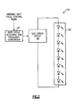
- Fig. 2 is a block diagram of a lighting device 10 incorporating embodiments of the present inventive subject matter.
- the lighting device 10 includes a driver circuit 20 and one or more LEDs 22.
- the LED driver circuit 20 is responsive to a duty cycle detection and frequency conversion circuit 24.
- the duty cycle detection and frequency conversion circuit 24 receives a variable duty cycle input signal of a first frequency and outputs a fixed amplitude signal having a second frequency different from the first frequency and with a duty cycle that is dependent on the duty cycle of the variable duty cycle input signal.
- the duty cycle of the output waveform of the duty cycle detection and frequency conversion circuit 24 may be substantially the same as the duty cycle of the input signal or it may differ according to a predefined relationship.
- the duty cycle of the output waveform may have a linear or non-linear relationship to the duty cycle of the input signal.
- the duty cycle of the output waveform will typically not track the duty cycle of the input waveform on a cycle by cycle basis. Such may be beneficial if substantial variations may occur in the duty cycle of the variable duty cycle waveform, for example as may occur in the output of a conventional AC phase cut dimmer even without changing the setting of the dimmer.
- the output waveform of the duty cycle detection and frequency conversion circuit 24 will, in some embodiments, have a duty cycle that is related to a smoothed or average duty cycle of the input signal.
- This smoothing or averaging of the input duty cycle may reduce the likelihood that unintended variations in the duty cycle of the input waveform will result in undesirable changes in intensity of the light output by the lighting device 10 while still allowing for changes in the dimming level. Further details on the operation of duty cycle detection and frequency conversion circuits according to some embodiments of the present inventive subject matter are provided below.
- Fig. 3 illustrates further embodiments of the present inventive subject matter where a lighting device 30 is powered from an AC line input where the duty cycle of the AC line input varies. Such an input may, for example, be provided by utilizing a phase cut dimmer to control the duty cycle of the AC line input.
- the lighting device 30 includes one or more LEDs 22, an LED driver circuit 40, a power supply 42 and a duty cycle detection and frequency conversion circuit 44.
- the power supply 42 receives an AC line input and provides power to the LED driver circuit 40 and the duty cycle detection and frequency conversion circuit 44.
- the power supply 42 may be any suitable power supply including, for example, buck or boost power supplies as described in United States Patent Application Serial No. 11/854,744 .
- the duty cycle detection and frequency conversion circuits 24 and/or 44 of Figs. 2 and/or 3 may also detect when the duty cycle of the input waveform has fallen below a minimum threshold and output a shutdown signal.
- the shutdown signal may be provided to the power supply 42 and/or the LED driver circuit 20 or 40. In some embodiments, the shutdown signal may be provided to turn off the LEDs at a time before the input power to the lighting device 10 or 30 reaches a level that is below a minimum operating level of the lighting device 10 or 30.
- the shutdown signal may be provided to turn off the LEDs at a time before the power drawn by the lighting device 10 or 30 reaches a level that is below a minimum operating power for a dimmer control device, such as a triac dimmer or other phase cut dimmer.
- a dimmer control device such as a triac dimmer or other phase cut dimmer.
- the output of the duty cycle detection circuit is provided to an averaging circuit 120 that creates an average value of the output of the duty cycle detection circuit.
- the average value is reflected as a voltage level.
- a high frequency waveform is provided by the waveform generator 130.
- the waveform generator 130 may generate a triangle, sawtooth or other periodic waveform.
- the frequency of the waveform output by the waveform generator 130 is greater than 200 Hz, and in particular embodiments, the frequency is about 300 Hz (or higher).
- the shape of the waveform may be selected to provide the desired relationship between the duty cycle of the input signal and the duty cycle of the frequency converted pulse width modulated (PWM) output.
- the output of the waveform generator 130 and the output of the averaging circuit 120 are compared by the comparator 140 to generate a periodic waveform with the frequency of the output of the waveform generator 130 and a duty cycle based on the output of the averaging circuit 120.
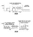
- Figs. 5A and 5B illustrate duty cycle detection utilizing a symmetric threshold ( Fig. 5A ) and alternative embodiments utilizing asymmetric thresholds ( Fig. 5B ). In either case, the voltage level of the input waveform is compared to a threshold voltage.
- the output of the duty cycle detection circuit 110 is set to a first voltage level (in this embodiment, 10 volts) and if the input voltage level is below the threshold voltage, the output of the duty cycle detection circuit 110 is set to a second voltage level (in this embodiment, 0 volts, i.e., ground).
- the output of the duty cycle detection circuit 110 is a square wave that transitions between the first voltage level and the second voltage level (e.g., 10 V and ground).
- the first and second voltage levels may be any suitable voltage levels and may be selected based upon the particular averaging circuit utilized.
- the output of the duty cycle detection circuit 110 is set to a first voltage level and remains at that voltage level until the input voltage level falls below a second threshold voltage at which time the output of the duty cycle detection circuit 110 is set to a second voltage level.
- the output of the duty cycle detection circuit 110 is also a square wave that transitions between the first voltage level and the second voltage level (e.g., 10 V and ground).
- the first and second voltage levels may be any suitable voltage levels and may be selected based upon the particular averaging circuit utilized. The asymmetric detection may allow for compensation for variations in the input waveform.
- This embodiment thus provides an averaged square wave signal which is related to the duty cycle of the input voltage. For example, if (1) the duty cycle of the input voltage is 60%, (2) the duty cycle of the output of the duty cycle detection circuit is 55%, (3) the first voltage level is 10 V and (4) the second voltage level is 0 V, the voltage of the averaged square wave signal would be about 5.5 V.
- the averaged square wave signal can instead be inversely related to the duty cycle of the input voltage.
- Fig. 6B illustrates the generation of the frequency shifted variable duty cycle output.
- the output of the comparator 140 is set to a first voltage level, and while the value of the output of the averaging circuit 120 is below the voltage of the output of the waveform generator 130, the output of the comparator 140 is set to a second voltage level, e.g., ground (i.e., whenever the plot of the voltage of the averaging circuit crosses the plot of the output of the waveform generator to become larger than the output of the waveform generator, the output of the comparator is switched to the first voltage level, and whenever the plot of the voltage of the averaging circuit crosses the plot of the output of the waveform generator to become smaller than the output of the waveform generator, the output of the comparator is switched to the second voltage level).
- the output of the comparator 140 is a square wave that transitions between the first voltage level and the second voltage level (e.g., 10 V and ground), has a duty cycle that corresponds to the level of the voltage output by the averaging circuit 120 and has a frequency corresponding to the frequency of the output of the waveform generator 130.
- the first and second voltage levels may be any suitable voltage levels and may be selected based upon the particular LED driver circuit with which the duty cycle detection and frequency conversion circuit 100 is being utilized.
- the comparator 140 is a square wave that transitions between the first voltage level and the second voltage level (e.g., 10 V and ground), has a duty cycle that corresponds to the level of the voltage output by the averaging circuit 120 and has a frequency corresponding to the frequency of the output of the waveform generator 130.
- the second voltage level e.g. 10 V and ground
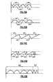
- FIG. 15D shows a linear waveform which consists of a repeating pattern which includes two differently-shaped sub-portions 204 and 205.
- Fig. 15E shows a non-linear waveform which consists of a repeating pattern which includes tow differently-shaped sub-portions 206 and 207. It is readily seen that there are an infinite number of possible waveforms, and persons skilled in the art can readily select any desired waveform in order to achieve desired characteristics.
- the voltage output by the averaging circuit could be increased such that where the duty cycle of the rectified power signal is 100%, the output of the averaging circuit is representative of a 100% duty cycle power signal (even though the output of the duty cycle detection circuit generated in response to the input waveform exhibits the first voltage level only part of the time, e.g., 95% of the time (and thus the averaged square wave represents a percentage duty cycle which is higher, e.g., by 5%, than the percentage of the time that the square wave representation of AC phase cut exhibits the first voltage level).
- the minimum pulse width detection circuit 150 allows for setting the low level dimming point by detecting when the voltage output by the averaging circuit 120 falls below (or above, in embodiments where the duty cycle of the output of the duty cycle detection circuit is inversely related to the duty cycle of the input voltage) a threshold voltage associated with the minimum duty cycle for which the lighting device and/or dimmer will operate reliably.
- the duty cycle detection and frequency conversion circuit 300 includes a slope adjust circuit 160.
- the slope adjust circuit 160 provides a method to offset the duty cycle ratio between the duty cycle determined from the variable duty cycle waveform, such as a rectified AC line with phase cut dimming, and the PWM output provided to the LED driver circuit. This would allow for a lower light level while still maintaining a sufficient AC voltage from the triac dimmer to power a lighting device.
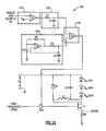
- Fig. 9 is a circuit diagram of a duty cycle detection and frequency conversion circuit 100 according to some embodiments of the present inventive subject matter.
- the rectified AC line voltage is scaled to appropriate voltage levels, for example, by dividing the voltage down through a resistor divider network, and sent to the positive input of a first comparator U1.
- the comparator U1 compares the scaled and rectified AC to a fixes voltage reference (V thr ) at the negative input.
- the resultant waveform is a fixed amplitude square wave with a duty cycle and a frequency which correspond to the duty cycle and frequency of the rectified AC line.
- the reference voltage V thr sets the maximum pulse width of the square wave output of the comparator U1. The closer the reference voltage V thr is to zero volts the greater the maximum pulse width (for example, if V thr is 5 V, the maximum pulse width is 100% minus the percentage of the time that the pulse is less than 5 V (the percentage of the time that the pulse is less than 5 V corresponding to the percentage of the plot, viewed along the x axis, where the plot is less than 5 V)).
- the output of the RC filter is provided to the positive input of a second comparator U3 and is compared to a fixed-frequency fixed-amplitude triangle/sawtooth wave generated by the op amp (i.e., operational amplifier) U2, resistors R2, R3 and R4 and the capacitor C2.
- the triangle/sawtooth waveform is connected to the negative input of the comparator U3 (in embodiments in which the duty cycle of the output of the duty cycle detection circuit is inversely related to the duty cycle of the input voltage, the waveform is instead connected to the positive input of the comparator U3 ).
- the output of the comparator U3 is a square wave which has a duty-cycle proportional to the voltage level at the positive input of the comparator U3 (the output of the averaging circuit 120 ) and a frequency equal to that of the triangle/sawtooth wave.
- the duty cycle of, for example, a lower frequency AC line can be translated to a higher frequency square wave.
- the square wave can be used to gate LEDs on and off for a dimming effect.
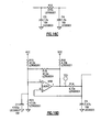
- Fig. 10 is a circuit diagram of a duty cycle detection and frequency conversion circuit 100' that provides asymmetric threshold voltages for duty cycle detection.
- the duty cycle detection circuit 110' includes a second comparator U4, a logic AND gate A1 and a Set/Reset latch L1 that provide independently settable on and off thresholds.
- the triac based AC waveform can have half cycle imbalances that the voltage threshold(s) critical may be set based upon to provide steady PWM duty cycle generation.
- the duty cycle detection circuit 110' sets the latch L1 when the input voltage becomes higher than the threshold voltage V 1 and resets the latch Ll when the input voltage falls below the threshold voltage V 2 , where V 1 > V 2 .
- V 1 the threshold voltage
- the output of the comparator U1 is high and the set input S of the latch Ll is high so as to cause the output Q of the latch Ll to go high.
- the output of the comparator U1 goes low but the output Q of the latch L1 remains high.
- Fig. 11 is a circuit diagram illustrating a duty cycle detection and frequency conversion circuit 200 that incorporates a minimum pulse width detection circuit 150.
- the minimum pulse width detection circuit 150 is provided by the comparator U5.
- a reference voltage V shut is provided to one input of the comparator U5 and the output of the averaging circuit 120 is provided to the other input.
- the output of the averaging circuit is related to the output of the duty cycle detection circuit. When the output of the averaging circuit falls below the reference voltage V shut , the output of the comparator U5 goes high, thus providing a shutdown signal.
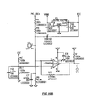
- Fig. 12 is a circuit diagram of a duty cycle detection circuit 100 coupled to an LED driver circuit where the string of LEDs (LED1, LED2 and LED3) is driven by an input voltage that is modulated by a high frequency drive signal through the transistor T1.
- the diode D1, capacitor C3 and inductor L1 provide current smoothing between cycles of the high frequency drive signal.
- the resistor R5 provides a current sense that can be fed back to a driver controller that varies the duty cycle of the high frequency drive signal to provide constant current to the LEDs.
- the gate of the transistor T1 is controlled by the driver DR1.
- the driver is enabled by the output of the duty cycle detection and frequency conversion circuit 100 so that the high frequency drive signal is controlled by the output of the duty cycle detection and frequency conversion circuit 100.
- the transistor T1 is controlled by the output of the duty cycle detection and frequency conversion circuit 100, it may be necessary to disable or otherwise control or compensate for the current sense feedback to the controller when the transistor T1 is off, as the sensed current feedback is only valid when the transistor T1 is on.
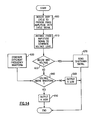
- Figs. 13 and 14 are flowchart illustrations of operations according to some embodiments of the present inventive subject matter. It will be appreciated that the operations illustrated in Figs. 13 and 14 may be carried out simultaneously or in different sequences without departing from the teachings of the present inventive subject matter. Thus, embodiments of the present inventive subject matter should not be construed as limited to the particular sequence of operations illustrated by the flowcharts. Furthermore, operations illustrated in the flowcharts may be carried out entirely in hardware or in combinations of hardware and software.
- the averaged voltage level is compared to the voltage of a generated waveform (block 640 ).
- the generated waveform is of a frequency different from that of the input signal (block 630 ). If the averaged voltage level is above the voltage of the generated waveform (block 640 ), a high signal is output (block 660 ). If the averaged voltage is below the voltage of the generated waveform (block 640 ), a low signal is output (block 650 ).
- a light or a set of lights connected to a driver as described herein can be connected to a power source, through a circuit in accordance with the present inventive subject matter, without concern as to the frequency of the voltage from the power source and/or the voltage level of the power source.
- the frequency of the line voltage is 50 Hz, 60 Hz, 100 Hz or other values (e.g., if connected to a generator, etc.) and/or in which the line voltage can change or vary, and the problems that can be caused, particularly with conventional dimmers, when connecting a light or set of lights to such line voltage.
- circuitry as described herein a light or set of lights can be connected to line voltages of widely differing frequencies and/or which vary in voltage level, with good results.
- a lighting control circuit can be configured such that when the duty cycle of the input voltage is a certain percentage (e.g., 10 %), the circuitry can cause the output of the device to have a particular color temperature (e.g., 2,000 K).
- a certain percentage e.g. 10 %
- the circuitry can cause the output of the device to have a particular color temperature (e.g., 2,000 K).
- a particular color temperature e.g., 2,000 K.
- the color temperature typically decreases, and it might be deemed desirable for the lighting device to mimic this behavior.
- circuits and methods according to the present inventive subject matter are not limited to AC power or to AC phase cut dimmers. Rather, the present inventive subject matter is applicable to all types of dimming using waveform duty cycle (e.g., including pulse width modulation).
Abstract
Description
- The present inventive subject matter relates to lighting devices and more particularly to power control for light emitting devices in the presence of a dimming signal where pulse width is a reflection of dimming level.
- Many control circuits for lighting utilize phase cut dimming. In phase cut dimming, the leading or trailing edge of the line voltage is manipulated to reduce the RMS voltage provided to the light. When used with incandescent lamps, this reduction in RMS voltage results in a corresponding reduction in current and, therefore, a reduction in power consumption and light output. As the RMS voltage decreases, the light output from the incandescent lamp decreases.
- Patent document
US 2003l0146715 A1 - An example of a cycle of a full wave rectified AC signal is provided in
Fig. 1A , a cycle of a phase cut rectified AC waveform is illustrated inFig. 1B and a cycle of a reverse phase cut AC waveform is illustrated inFig. 1C . As seen inFigs. 1A through 1C , when phase cut dimming is utilized, the duty cycle of the resulting rectified waveform is changed. This change in duty cycle, if sufficiently large, is noticeable as a decrease in light output from an incandescent lamp. The "off" time does not result in flickering of the incandescent lamp because the filament of an incandescent lamp has some thermal inertia and will remain at a sufficient temperature to emit light even during the "off" time when no current flows through the filament. - Recently, solid state lighting systems have been developed that provide light for general illumination. These solid state lighting systems utilize light emitting diodes or other solid state light sources that are coupled to a power supply that receives the AC line voltage and converts that voltage to a voltage and/or current suitable for driving the solid state light emitters. Typical power supplies for light emitting diode light sources include linear current regulated supplies and/or pulse width modulated current and/or voltage regulated supplies.
- Many different techniques have been described for driving solid state light sources in many different applications, including, for example, those described in United States Patent No.
3,755,697 to Miller , United States Patent No.5,345,167 to Hasegawa et al , United States Patent No.5,736,881 to Ortiz , United States Patent No.6,150,771 to Perry , United States Patent No.6,329,760 to Bebenroth , United States Patent No.6,873,203 to Latham, II et al , United States Patent No.5,151,679 to Dimmick , United States Patent No.4,717,868 to Peterson , United States Patent No.5,175,528 to Choi et al , United States Patent No.3,787,752 to Delay , United States Patent No.5,844,377 to Anderson et al , United States Patent No.6,285,139 to Ghanem , United States Patent No.6,161,910 to Reisenauer et al , United States Patent No.4,090,189 to Fisler , United States Patent No.6,636,003 to Rahm et al , United States Patent No.7,071,762 to Xu et al , United States Patent No.6,400,101 to Biebl et al , United States Patent No.6,586,890 to Min et al , United States Patent No.6,222,172 to Fossum et al , United States Patent No.5,912,568 to Kiley , United States Patent No.6,836,081 to Swanson et al , United States Patent No.6,987,787 to Mick , United States Patent No.7,119,498 to Baldwin et al , United States Patent No.6,747,420 to Barth et al , United States Patent No.6,808,287 to Lebens et al , United States Patent No.6,841,947 to Berg-johansen , United States Patent No.7,202,608 to Robinson et al , United States Patent No,6,995,518 , United States Patent No.6,724,376 , United States Patent No.7,180,487 to Kamikawa et al , United States Patent No.6,614,358 to Hutchison et al , United States Patent No.6,362,578 to Swanson et al , United States Patent No.5,661,645 to Hochstein , United States Patent No.6,528,954 to Lys et al , United States Patent No.6,340,868 to Lys et al , United States Patent No.7,038,399 to Lys et al , United States Patent No.6,577,072 to Saito et al , and United States Patent No.6,388,393 to Illingworth . - In the general illumination application of solid state light sources, one desirable characteristic is to be compatible with existing dimming techniques. In particular, dimming that is based on varying the duty cycle of the line voltage may present several challenges in power supply design for solid state lighting. Unlike incandescent lamps, LEDs typically have very rapid response times to changes in current. This rapid response of LEDs may, in combination with conventional dimming circuits, present difficulties in driving LEDs.
- For example, one way to reduce the light output in response to the phase cut AC signal is to utilize the pulse width of the incoming phase cut AC line signal to directly control the dimming of the LEDs. The 120 Hz signal of the full-wave rectified AC line signal would have a pulse width the same as the input AC signal. This technique limits the ability to dim the LEDs to levels below where there is insufficient input power to energize the power supply. Also, at narrow pulse width of the AC signal, the output of the LEDs can appear to flicker, even at the 120 Hz frequency. This problem may be exacerbated in 50 Hz systems as the full wave rectified frequency of the AC line is only 100 Hz.
- Furthermore, variation in the input signal may affect the ability to detect the presence of a phase cut dimmer or may make detection unreliable. For example, in systems that detect the presence of a phase cut dimmer based on detection of the leading edge of the phase cut AC input, if a reverse-phase cut dimmer is used, the dimming is never detected. Likewise, many residential dimmers have substantial variation in pulse width even without changing the setting of a dimmer. If a power supply detects the presence of dimming based on a threshold pulse width, the power supply could detect the presence of dimming on one cycle and not on another as a result of this the variation in pulse width.
- A further issue relates to AC dimmers providing some phase cut even at "full on." If the LEDs are directly controlled by the AC pulse width, then the LEDs may never reach full output but will dim the output based on the pulse width of the "full on" signal. This can result in a large dimming of output. For example, an incandescent lamp might see a 5% reduction in power when the pulse width is decreased 20%. Many incandescent dimmers have a 20% cut in pulse width at full on, even though the RMS voltage is only reduced 5%. While this would result in a 5% decrease in output of an incandescent, it results in a 20% decrease in output if the phase cut signal is used to directly control the LEDs.
- The frequency converted dimming circuits described herein may overcome one or more of the problems associated with dimming directly from a phase cut input AC line. Embodiments of the present inventive subject matter may be particularly well suited to controlling a drive circuit for solid state lighting devices, such as LEDs. In particular, an input waveform with an input frequency and duty cycle are converted to an output waveform with an output frequency with a duty cycle that is based on the input duty cycle. In some embodiments, the output frequency is greater than the input frequency. For example, when the input waveform is a phase cut AC line input, the output frequency may be greater than the input frequency so as to reduce or eliminate the perception of flicker in a lighting device that is dimmed by the phase cut of the AC line input. By increasing the switching frequency, the flicker becomes undetectable to the human eye, but the integrated value of duty-cycle of the light remains, effectively dimming the LEDs.
- The invention will now be further described, by way of example only, with reference to the accompanying drawings, in which:
-
Figs. 1A through 1C are examples of a cycle of a full wave rectified AC line signal with and without phase cut dimming. -
Fig. 2 is a block diagram of a lighting device incorporating duty cycle detection and frequency conversion according to some embodiments of the present inventive subject matter. -
Fig. 3 is a block diagram of a lighting device suitable for use in an AC phase cut dimming system according to some embodiments of the present inventive subject matter. -
Fig. 4 is a block diagram of a duty cycle detection and frequency conversion circuit according to some embodiments of the present inventive subject matter. -
Figs. 5A and 5B are waveform diagrams illustrating alternative duty cycle detection techniques suitable for use in duty cycle detection circuits according to some embodiments of the present inventive subject matter. -
Figs. 6A and 6B are timing diagrams illustrating operation of averaging, waveform generator and comparator circuits according to some embodiments of the present inventive subject matter. -
Fig. 7 is a block diagram of a duty cycle detection and frequency conversion circuit according to further embodiments of the present inventive subject matter. -
Fig. 8 is a block diagram of a duty cycle detection and frequency conversion circuit according to further embodiments of the present inventive subject matter. -
Fig. 9 is a circuit diagram of a duty cycle detection and frequency conversion circuit utilizing symmetric pulse width detection according to some embodiments of the present inventive subject matter. -
Fig. 10 is a circuit diagram of a duty cycle detection and frequency conversion circuit utilizing asymmetric pulse width detection according to further embodiments of the present inventive subject matter. -
Fig. 11 is a circuit diagram of a duty cycle detection and frequency conversion circuit according to further embodiments of the present inventive subject matter. -
Fig. 12 is a circuit diagram of a system as illustrated inFig. 2 according to some embodiments of the present inventive subject matter. -
Fig. 13 is a flowchart illustration of operations of some embodiments of the present inventive subject matter. -
Fig. 14 is a flowchart illustration of operations according to further embodiments of the present inventive subject matter. -
Figs. 15A through 15E are representative examples of waveform shapes for the waveform generator according to the present inventive subject matter. -
Figs. 16A - 16F are circuit diagrams depicting an embodiment of a circuit according to the present inventive subject matter. - The present inventive subject matter now will be described more fully hereinafter with reference to the accompanying drawings, in which embodiments of the inventive subject matter are shown. However, this inventive subject matter should not be construed as limited to the embodiments set forth herein. Rather, these embodiments are provided so that this disclosure will be thorough and complete, and will fully convey the scope of the inventive subject matter to those skilled in the art. Like numbers refer to like elements throughout. As used herein, the term "and/or" includes any and all combinations of one or more of the associated listed items.
- The terminology used herein is for the purpose of describing particular embodiments only and is not intended to be limiting of the inventive subject matter. As used herein, the singular forms "a", "an" and "the" are intended to include the plural forms as well, unless the context clearly indicates otherwise. It will be further understood that the terms "comprises" and/or "comprising," when used in this specification, specify the presence of stated features, integers, steps, operations, elements, and/or components, but do not preclude the presence or addition of one or more other features, integers, steps, operations, elements, components, and/or groups thereof.
- As noted above, the various aspects of the present inventive subject matter include various combinations of electronic components (transformers, switches; diodes, capacitors, transistors, etc.). Persons skilled in the art are familiar with and have access to a wide variety of such components, and any of such components can be used in making the devices according to the present inventive subject matter. In addition, persons skilled in the art are able to select suitable components from among the various choices based on requirements of the loads and the selection of other components in the circuitry. Any of the circuits described herein (and/or any portions of such circuits) can be provided in the form of (1) one or more discrete components, (2) one or more integrated circuits, or (3) combinations of one or more discrete components and one or more integrated circuits.
- A statement herein that two components in a device are "electrically connected," means that there are no components electrically between the components that materially affect the function or functions provided by the device. For example, two components can be referred to as being electrically connected, even though they may have a small resistor between them which does not materially affect the function or functions provided by the device (indeed, a wire connecting two components can be thought of as a small resistor); likewise, two components can be referred to as being electrically connected, even though they may have an additional electrical component between them which allows the device to perform an additional function, while not materially affecting the function or functions provided by a device which is identical except for not including the additional component; similarly, two components which are directly connected to each other, or which are directly connected to opposite ends of a wire or a trace on a circuit board or another medium, are electrically connected.
- Although the terms "first", "second", etc. may be used herein to describe various elements, components, regions, layers, sections and/or parameters, these elements, components, regions, layers, sections and/or parameters should not be limited by these terms. These terms are only used to distinguish one element, component, region, layer or section from another region, layer or section. Thus, a first element, component, region, layer or section discussed below could be termed a second element, component, region, layer or section without departing from the teachings of the present inventive subject matter.
- Unless otherwise defined, all terms (including technical and scientific terms) used herein have the same meaning as commonly understood by one of ordinary skill in the art to which this inventive subject matter belongs. It will be further understood that terms, such as those defined in commonly used dictionaries, should be interpreted as having a meaning that is consistent with their meaning in the context of the relevant art and the present disclosure and will not be interpreted in an idealized or overly formal sense unless expressly so defined herein.
-
Fig. 2 is a block diagram of alighting device 10 incorporating embodiments of the present inventive subject matter. As seen inFig. 2 , thelighting device 10 includes adriver circuit 20 and one ormore LEDs 22. TheLED driver circuit 20 is responsive to a duty cycle detection and frequency conversion circuit 24. The duty cycle detection and frequency conversion circuit 24 receives a variable duty cycle input signal of a first frequency and outputs a fixed amplitude signal having a second frequency different from the first frequency and with a duty cycle that is dependent on the duty cycle of the variable duty cycle input signal. - The duty cycle of the output waveform of the duty cycle detection and frequency conversion circuit 24 may be substantially the same as the duty cycle of the input signal or it may differ according to a predefined relationship. For example, the duty cycle of the output waveform may have a linear or non-linear relationship to the duty cycle of the input signal. Likewise, the duty cycle of the output waveform will typically not track the duty cycle of the input waveform on a cycle by cycle basis. Such may be beneficial if substantial variations may occur in the duty cycle of the variable duty cycle waveform, for example as may occur in the output of a conventional AC phase cut dimmer even without changing the setting of the dimmer. Therefore, the output waveform of the duty cycle detection and frequency conversion circuit 24 will, in some embodiments, have a duty cycle that is related to a smoothed or average duty cycle of the input signal. This smoothing or averaging of the input duty cycle may reduce the likelihood that unintended variations in the duty cycle of the input waveform will result in undesirable changes in intensity of the light output by the
lighting device 10 while still allowing for changes in the dimming level. Further details on the operation of duty cycle detection and frequency conversion circuits according to some embodiments of the present inventive subject matter are provided below. - The
driver circuit 20 may be any suitable driver circuit capable of responding to a pulse width modulated input that reflects the level of dimming of theLEDs 22. The particular configuration of theLED driver circuit 20 will depend on the application of thelighting device 10. For example, the driver circuit may be a boost or buck power supply. Likewise, theLED driver circuit 20 may be a constant current or constant voltage pulse width modulated power supply. For example, the LED driver circuit may be as described in United States Patent No.7,071,762 . Alternatively, theLED driver circuit 20 may be a driver circuit using linear regulation, such as described in United States Patent No.7,038,399 and inU.S. Patent Application No. 60/844,325, filed on September 13, 2006 U.S. Patent Application No. 11/854,744, filed September 13, 2007 LED driver circuit 20 will depend on the application of thelighting device 10. -
Fig. 3 illustrates further embodiments of the present inventive subject matter where alighting device 30 is powered from an AC line input where the duty cycle of the AC line input varies. Such an input may, for example, be provided by utilizing a phase cut dimmer to control the duty cycle of the AC line input. Thelighting device 30 includes one ormore LEDs 22, anLED driver circuit 40, apower supply 42 and a duty cycle detection andfrequency conversion circuit 44. Thepower supply 42 receives an AC line input and provides power to theLED driver circuit 40 and the duty cycle detection andfrequency conversion circuit 44. Thepower supply 42 may be any suitable power supply including, for example, buck or boost power supplies as described in United States Patent Application Serial No.11/854,744 LED driver circuit 40 may be any suitable LED driver circuit capable of varying the intensity of the output of theLEDs 22 in response to a fixed amplitude signal of variable duty cycle. The particular configurations of theLED driver circuit 40 and/or thepower supply 42 will depend on the application of thelighting device 30. - As is further seen in
Fig. 3 , the duty cycle detection andfrequency conversion circuit 44 receivers the rectified AC input from thepower supply 42 and detects the duty cycle of the rectified AC input. By detecting duty cycle rather than RMS voltage, the duty cycle detection andfrequency conversion circuit 44 may be less sensitive to variations in the AC input voltage (for example, if duty cycle were estimated by instead tacking RMS voltage, an AC line voltage drop from 120VAC to 108VAC would bring about an incorrect reduction in the estimated duty cycle, i.e., variations in input voltage may be misinterpreted as changes in duty cycle and result in an undesired dimming of the light output). In contrast, by detecting duty cycle rather than RMS voltage, variations in the voltage level will only be reflected as small variations in the detected duty cycle that result from changes in slew rate for the voltage to reach the differing voltage levels. - In addition to generating a frequency converted fixed amplitude waveform having a duty cycle that is related to the duty cycle of the input wave form, the duty cycle detection and frequency conversion circuits 24 and/or 44 of
Figs. 2 and/or 3 may also detect when the duty cycle of the input waveform has fallen below a minimum threshold and output a shutdown signal. The shutdown signal may be provided to thepower supply 42 and/or theLED driver circuit lighting device lighting device lighting device -
Fig. 4 illustrates functional blocks for a duty cycle detection andfrequency conversion circuit 100 according to some embodiments of the present inventive subject matter. The duty cycle detection andfrequency conversion circuit 100 utilizes pulse width detection of a variable duty cycle waveform to provide a dutycycle detection circuit 110. The output of the dutycycle detection circuit 110 is a fixed amplitude waveform with a duty cycle corresponding to (i.e., based on, but not necessarily differing from) the duty cycle of the input waveform (e.g., depending on the embodiment according to the present inventive subject matter, similar to, slightly less than, related to or inversely related to the duty cycle of the input waveform). The expression "related to" encompasses relationships where the variance of the duty cycle of the output of the duty cycle detection circuit is proportional to the variance of the duty cycle of the input waveform (i.e., there is a linear relationship between the two), or where there is no linear relationship and if the duty cycle of the input waveform increases, the duty cycle of the output of the duty cycle detection circuit also increases, and vice-versa (i.e., if the duty cycle of the input waveform decreases, the duty cycle of the output of the duty cycle detection circuit also decreases); conversely, the expression "inversely related to" encompasses relationships where the variance of the duty cycle of the output of the duty cycle detection circuit is inversely proportional to the variance of the duty cycle of the input waveform, or where there is no linear inverse relationship and if the duty cycle of the input waveform decreases, the duty cycle of the output of the duty cycle detection circuit increases, and vice-versa. - The output of the duty cycle detection circuit is provided to an
averaging circuit 120 that creates an average value of the output of the duty cycle detection circuit. In some embodiments, the average value is reflected as a voltage level. A high frequency waveform is provided by thewaveform generator 130. Thewaveform generator 130 may generate a triangle, sawtooth or other periodic waveform. In some embodiments, the frequency of the waveform output by thewaveform generator 130 is greater than 200 Hz, and in particular embodiments, the frequency is about 300 Hz (or higher). The shape of the waveform may be selected to provide the desired relationship between the duty cycle of the input signal and the duty cycle of the frequency converted pulse width modulated (PWM) output. The output of thewaveform generator 130 and the output of the averagingcircuit 120 are compared by thecomparator 140 to generate a periodic waveform with the frequency of the output of thewaveform generator 130 and a duty cycle based on the output of the averagingcircuit 120. - Operation of a first embodiment of a duty cycle detection and
frequency conversion circuit 100 will now be described with reference to the waveform diagrams ofFigs. 5A, 5B ,6A and 6B . In particular,Figs. 5A and 5B illustrate duty cycle detection utilizing a symmetric threshold (Fig. 5A ) and alternative embodiments utilizing asymmetric thresholds (Fig. 5B ). In either case, the voltage level of the input waveform is compared to a threshold voltage. - In the symmetric example (
Fig. 5A ), if the input voltage is above the threshold voltage, the output of the dutycycle detection circuit 110 is set to a first voltage level (in this embodiment, 10 volts) and if the input voltage level is below the threshold voltage, the output of the dutycycle detection circuit 110 is set to a second voltage level (in this embodiment, 0 volts, i.e., ground). Thus, the output of the dutycycle detection circuit 110 is a square wave that transitions between the first voltage level and the second voltage level (e.g., 10 V and ground). The first and second voltage levels may be any suitable voltage levels and may be selected based upon the particular averaging circuit utilized. - In the asymmetric example (
Fig. 5B ), if the input voltage is above a first threshold, the output of the dutycycle detection circuit 110 is set to a first voltage level and remains at that voltage level until the input voltage level falls below a second threshold voltage at which time the output of the dutycycle detection circuit 110 is set to a second voltage level. Thus, in the asymmetric example, the output of the dutycycle detection circuit 110 is also a square wave that transitions between the first voltage level and the second voltage level (e.g., 10 V and ground). As described above, the first and second voltage levels may be any suitable voltage levels and may be selected based upon the particular averaging circuit utilized. The asymmetric detection may allow for compensation for variations in the input waveform. For example, if the leading or trailing edges of a phase cut waveform intermittently include a section with a shallow slope followed or preceded by a section with a steep slope, the separate thresholds could be set to align with the section of steep slope so as to avoid minor variations in duty cycle being amplified by the shallow slope portions of the waveform. -
Fig. 6A illustrates operation of the averagingcircuit 120. As seen inFig. 6A , the averagingcircuit 120 averages a fixed amplitude periodic waveform with varying duty cycle to provide an averaged square wave signal having a voltage that (in this embodiment) represents the duty cycle of the input waveform. The level of averaging may be set to smooth out variations in the duty cycle of the input signal. - This embodiment thus provides an averaged square wave signal which is related to the duty cycle of the input voltage. For example, if (1) the duty cycle of the input voltage is 60%, (2) the duty cycle of the output of the duty cycle detection circuit is 55%, (3) the first voltage level is 10 V and (4) the second voltage level is 0 V, the voltage of the averaged square wave signal would be about 5.5 V. Alternatively, in other embodiments according to the present inventive subject matter, the averaged square wave signal can instead be inversely related to the duty cycle of the input voltage. For example, if the first voltage level is ground and the second voltage level is 10 V, the inverse relationship would be provided (to illustrate, for such an embodiment, if (1) the duty cycle of the input voltage is 85% and the threshold voltage is 0 V (e.g., zero cross detection AC sensing is employed), the duty cycle of the output of the duty cycle detection circuit would be 15% (i.e., for 85 % of the time, the voltage level would be ground, which is the first voltage level, and for 15 % of the time, the voltage level would be 10 V, which is the second voltage level), such that the voltage of the averaged square wave signal would be about 1.5 V (whereas is the duty cycle of the input voltage were 10%, the voltage of the averaged square wave signal would be about 9 V).
- It should also be noted that it is not necessary for either of the first voltage level or the second voltage level to be zero. For instance, if (1) the duty cycle of the input voltage is 80%, (2) the duty cycle of the output of the duty cycle detection circuit is 70%, (3) the first voltage level is 20 V and (4) the second voltage level is 10 V, the voltage of the averaged square wave signal would be about 17 V (i.e., the voltage of the averaged square wave signal would be between 10 V and 20 V, and would vary within that range proportionally to the duty cycle of the output of the duty cycle detection circuit.
-
Fig. 6B illustrates the generation of the frequency shifted variable duty cycle output. As seen inFig. 6B , while the voltage of the averaged square wave signal (i.e., the output of the averaging circuit 120) is greater than the voltage of the output of thewaveform generator 130, the output of thecomparator 140 is set to a first voltage level, and while the value of the output of the averagingcircuit 120 is below the voltage of the output of thewaveform generator 130, the output of thecomparator 140 is set to a second voltage level, e.g., ground (i.e., whenever the plot of the voltage of the averaging circuit crosses the plot of the output of the waveform generator to become larger than the output of the waveform generator, the output of the comparator is switched to the first voltage level, and whenever the plot of the voltage of the averaging circuit crosses the plot of the output of the waveform generator to become smaller than the output of the waveform generator, the output of the comparator is switched to the second voltage level). Thus, the output of thecomparator 140 is a square wave that transitions between the first voltage level and the second voltage level (e.g., 10 V and ground), has a duty cycle that corresponds to the level of the voltage output by the averagingcircuit 120 and has a frequency corresponding to the frequency of the output of thewaveform generator 130. The first and second voltage levels may be any suitable voltage levels and may be selected based upon the particular LED driver circuit with which the duty cycle detection andfrequency conversion circuit 100 is being utilized. - In embodiments in which the duty cycle of the duty cycle detection circuit is inversely related to the input voltage (as discussed above), while the voltage of the averaged square wave signal (i.e., the output of the averaging circuit 120) is greater than the voltage of the output of the
waveform generator 130, the output of thecomparator 140 is instead set to a second voltage level (e.g., ground), and while the value of the output of the averagingcircuit 120 is below the voltage of the output of thewaveform generator 130, the output of thecomparator 140 is instead set to a first voltage level, with the result that, as with the embodiment shown inFig. 6B , thecomparator 140 is a square wave that transitions between the first voltage level and the second voltage level (e.g., 10 V and ground), has a duty cycle that corresponds to the level of the voltage output by the averagingcircuit 120 and has a frequency corresponding to the frequency of the output of thewaveform generator 130. - While
Fig. 6B illustrates a generated waveform in the shape of a triangular sawtooth, any desired waveform shape can be employed. For example, the waveform can be of any of the shapes depicted inFigs. 15A through 15E. Fig. 15A shows a non-linear waveform which includeslinear portions 201 andcurved portions 202 in a repetitive pattern.Fig. 15B shows a non-linear waveform which also includeslinear portions 201 andcurved portions 202 in a repetitive pattern.Fig. 15C shows a linear waveform which includeslinear portions Fig. 15D shows a linear waveform which consists of a repeating pattern which includes two differently-shapedsub-portions Fig. 15E shows a non-linear waveform which consists of a repeating pattern which includes tow differently-shapedsub-portions - As can be seen from
Figs. 5A through 6B , the shape of the waveform output from thewaveform generator 130 may affect the relationship between the input voltage duty cycle and the output duty cycle of the duty cycle detection andfrequency conversion circuit 100. If the waveform is linear (i.e., consists of linear and/or substantially linear segments) in the range over which the voltage output by the averagingcircuit 120 operates, then the relationship between input duty cycle and output duty cycle will be linear. If the waveform is non-linear in at least part of the range over which the voltage output by the averagingcircuit 120 operates, then the relationship between input duty cycle and output duty cycle will be non-linear. - Likewise, offsets between the input duty cycle and the output duty cycle may be provided by a DC offset which adjusts the waveform output from the
waveform generator 130 and/or the voltage level output from the averagingcircuit 120. For example, in a system in which the voltage level of the averaged square wave is related to (or proportional to) the duty cycle of the input voltage, and in which the frequency shifted variable duty cycle output is a first voltage level when the voltage of the averaged square wave signal is greater than the voltage of the output of the waveform generator, if the output of thewaveform generator 130 is offset such that the highest voltage level reached by the waveform is lower than the voltage output by the averagingcircuit 120 with duty cycles of 90% or higher, then the output of the comparator would be a constant (DC) signal at the first voltage level except when the duty cycle of the input waveform falls below (i.e., is less than) 90%. Such variations could be made adjustable and/or selectable, for example, by a user. A variety of other relationships could be used, e.g., if the voltage level of the averaged square wave is inversely related to the duty cycle of the input voltage, and the frequency shifted variable duty cycle output is a first voltage level when the voltage of the averaged square wave signal is less than the voltage of the output of the waveform generator, the waveform generator can be offset such that the lowest voltage level reached by the waveform is higher than the voltage output by the averaging circuit with duty cycles of 90% or higher, such that the output of the comparator would likewise be a constant (DC) signal at the first voltage level except when the duty cycle of the input waveform falls below 90%. - Another representative example of an offset that can optionally be provided is a DC offset in which the voltage output by the averaging circuit is increased by a specific amount (i.e., in systems where the voltage level of the averaged square wave is related to the duty cycle of the input voltage) or decreased by a specific amount (i.e., in systems where the voltage level of the averaged square wave is inversely related to the duty cycle of the input voltage). Such an offset can be useful for a variety of purposes, e.g., to compensate for a circuit in which duty cycle detection (symmetric or asymmetric) does not use zero cross detection, such that even a 100% duty cycle rectified power signal would not produce a constant signal (i.e., where the voltage depicted in
Fig. 6A would be at thefirst voltage level 100% of the time). In such a situation, the voltage output by the averaging circuit could be increased such that where the duty cycle of the rectified power signal is 100%, the output of the averaging circuit is representative of a 100% duty cycle power signal (even though the output of the duty cycle detection circuit generated in response to the input waveform exhibits the first voltage level only part of the time, e.g., 95% of the time (and thus the averaged square wave represents a percentage duty cycle which is higher, e.g., by 5%, than the percentage of the time that the square wave representation of AC phase cut exhibits the first voltage level). -
Fig. 7 illustrates further embodiments of the present inventive subject matter where the duty cycle detection andfrequency conversion circuit 200 also includes a minimum pulse width detection feature. Many triac based dimmers have performance problems at light load levels which can be present with LED based lighting products at low duty cycle dimming levels. If the triac dimmers fall below their minimum load level, their output may be unpredictable, which may result in unpredictable output from a lighting device connected to the dimmer. Likewise, if the pulse width is too small, the minimum voltage requirements of the lighting device may not be met and the power supply might be starved for power. This condition may also be undesirable. As such, the ability to shut down a power supply or lighting device before the undesirable conditions resulting from low pulse width on the line input can avoid unpredictable and undesirable performance of the lighting device. Thus, the minimum pulsewidth detection circuit 150 allows for setting the low level dimming point by detecting when the voltage output by the averagingcircuit 120 falls below (or above, in embodiments where the duty cycle of the output of the duty cycle detection circuit is inversely related to the duty cycle of the input voltage) a threshold voltage associated with the minimum duty cycle for which the lighting device and/or dimmer will operate reliably. -
Fig. 8 illustrates still further embodiments of the present inventive subject matter. As seen inFig. 8 , the duty cycle detection andfrequency conversion circuit 300 includes a slope adjustcircuit 160. The slope adjustcircuit 160 provides a method to offset the duty cycle ratio between the duty cycle determined from the variable duty cycle waveform, such as a rectified AC line with phase cut dimming, and the PWM output provided to the LED driver circuit. This would allow for a lower light level while still maintaining a sufficient AC voltage from the triac dimmer to power a lighting device. -
Fig. 9 is a circuit diagram of a duty cycle detection andfrequency conversion circuit 100 according to some embodiments of the present inventive subject matter. As seen inFig. 9 , the rectified AC line voltage is scaled to appropriate voltage levels, for example, by dividing the voltage down through a resistor divider network, and sent to the positive input of a first comparator U1. The comparator U1 compares the scaled and rectified AC to a fixes voltage reference (Vthr) at the negative input. When the positive input exceeds the negative, the output of the comparator U1 is high; when the reverse is true, the output is low (on the other hand, in embodiments where the duty cycle of the output of the duty cycle detection circuit is inversely related to the duty cycle of the input voltage, the comparator U1 is reversed, such that the rectified AC input voltage is supplied to the negative input of the comparator U1 and the fixed voltage reference is supplied to the positive input of the comparator U1). The resultant waveform is a close representation of the non-zero voltage duty-cycle of the AC line (the closer the fixed voltage reference Vthr is to zero, the closer the resultant waveform approximates the non-zero voltage duty cycle of the AC line). The resultant waveform is a fixed amplitude square wave with a duty cycle and a frequency which correspond to the duty cycle and frequency of the rectified AC line. The reference voltage Vthr sets the maximum pulse width of the square wave output of the comparator U1. The closer the reference voltage Vthr is to zero volts the greater the maximum pulse width (for example, if Vthr is 5 V, the maximum pulse width is 100% minus the percentage of the time that the pulse is less than 5 V (the percentage of the time that the pulse is less than 5 V corresponding to the percentage of the plot, viewed along the x axis, where the plot is less than 5 V)). In some embodiments, the reference voltage may be set to a value that reduces or eliminates half cycle imbalances in a rectified triac phase cut AC waveform. Skilled artisans are familiar with ways to make the reference voltage zero (or very close to zero), e.g., by providing AC sensing detection, such as zero cross detection. - The variable duty-cycle fixed amplitude square wave from the duty
cycle detection circuit 110 is then filtered by the averagingcircuit 120 to create an average value; higher level for higher duty-cycles, lower level for lesser duty-cycles (the opposite is of course true in embodiments where the duty cycle of the output of the duty cycle detection circuit is inversely related to the duty cycle of the input voltage). Because the square wave is of fixed amplitude, the average value is proportional to the duty cycle of the square wave, which is proportional to the duty-cycle of the input waveform, such as the AC line input. The averagingcircuit 120 is illustrated as a filter that includes resistor R1 and capacitor C1. While a single stage RC filter is illustrated inFig. 9 , other filtering or averaging techniques could be utilized. For example, in some embodiments, an RC filter with two or more stages may be used. - The output of the RC filter is provided to the positive input of a second comparator U3 and is compared to a fixed-frequency fixed-amplitude triangle/sawtooth wave generated by the op amp (i.e., operational amplifier) U2, resistors R2, R3 and R4 and the capacitor C2. The triangle/sawtooth waveform is connected to the negative input of the comparator U3 (in embodiments in which the duty cycle of the output of the duty cycle detection circuit is inversely related to the duty cycle of the input voltage, the waveform is instead connected to the positive input of the comparator U3). The output of the comparator U3 is a square wave which has a duty-cycle proportional to the voltage level at the positive input of the comparator U3 (the output of the averaging circuit 120) and a frequency equal to that of the triangle/sawtooth wave. In this manner, the duty cycle of, for example, a lower frequency AC line can be translated to a higher frequency square wave. The square wave can be used to gate LEDs on and off for a dimming effect.
-
Fig. 9 illustrates the use of a single op amp sawtooth generator as thewaveform generator 130. Other circuits may also be utilized to generate appropriate waveforms. For example, a two op amp triangle oscillator as described on page A-44 of "Op Amps for Everyone," R. Mancini, Editor, September 2000, may also be utilized. Other circuits known to those of skill in the art may also be used. When using a waveform generator such as illustrated inFig. 9 , to provide a linear relationship (or substantially linear relationship) between input and output duty cycle, the portions of the resulting waveform for the range over which the average value voltage will vary should be linear (or substantially linear). For example, the waveform generator illustrated inFig. 9 may provide a waveform with a linear region and a non-linear region that resembles a "shark fin." If the range of voltages output by the averagingcircuit 120 overlaps with the non-linear region, then a small change in input duty cycle could result in a large change in output duty cycle, or vice-versa. Such a situation may make the overall circuit susceptible to noise or too sensitive to variations in input duty cycle (e.g. too sensitive to user input at a dimmer). As a result, the circuit illustrated inFig. 9 may be implemented such that the voltage range of the averagingcircuit 120 corresponds to a linear portion or portions of the output waveform from thewaveform generator 130. -
Fig. 10 is a circuit diagram of a duty cycle detection and frequency conversion circuit 100' that provides asymmetric threshold voltages for duty cycle detection. A seen inFig. 10 , the duty cycle detection circuit 110' includes a second comparator U4, a logic AND gate A1 and a Set/Reset latch L1 that provide independently settable on and off thresholds. As discussed above, the triac based AC waveform can have half cycle imbalances that the voltage threshold(s) critical may be set based upon to provide steady PWM duty cycle generation. - In operation, the duty cycle detection circuit 110' sets the latch L1 when the input voltage becomes higher than the threshold voltage V1 and resets the latch Ll when the input voltage falls below the threshold voltage V2, where V1 > V2. In particular, when the input voltage exceeds V1, the output of the comparator U1 is high and the set input S of the latch Ll is high so as to cause the output Q of the latch Ll to go high. When the input voltage falls below V1, the output of the comparator U1 goes low but the output Q of the latch L1 remains high. When the input further falls below V2, the output of the comparator U4 goes high, therefore both inputs to the AND gate A1 are high so the output of the AND gate A1 goes high, resetting the latch L1, and the output Q goes low. While the circuit illustrated in
Fig. 10 has been designed for V1 > V2, a corresponding circuit where V1 < V2 could be readily provided by logically ANDing the inverted output of the latch L1 with the output of comparator U1 and using the output of the AND as the set signal for the latch L1. In such a case, the AND gate A1 could be eliminated and the output of the comparator U4 provided directly to the rest of the latch L1. -
Fig. 11 is a circuit diagram illustrating a duty cycle detection andfrequency conversion circuit 200 that incorporates a minimum pulsewidth detection circuit 150. As seen inFig. 11 , the minimum pulsewidth detection circuit 150 is provided by the comparator U5. In particular, a reference voltage Vshut is provided to one input of the comparator U5 and the output of the averagingcircuit 120 is provided to the other input. In this embodiment, the output of the averaging circuit is related to the output of the duty cycle detection circuit.
When the output of the averaging circuit falls below the reference voltage Vshut, the output of the comparator U5 goes high, thus providing a shutdown signal. In alternative embodiments, in which the output of the averaging circuit is inversely related to the output of the duty cycle detection circuit, the output of the comparator U5 goes high to provide a shutdown signal when the output of the averaging circuit rises above the reference voltage Vshut. -
Fig. 12 is a circuit diagram of a dutycycle detection circuit 100 coupled to an LED driver circuit where the string of LEDs (LED1, LED2 and LED3) is driven by an input voltage that is modulated by a high frequency drive signal through the transistor T1. The diode D1, capacitor C3 and inductor L1 provide current smoothing between cycles of the high frequency drive signal. The resistor R5 provides a current sense that can be fed back to a driver controller that varies the duty cycle of the high frequency drive signal to provide constant current to the LEDs. The gate of the transistor T1 is controlled by the driver DR1. The driver is enabled by the output of the duty cycle detection andfrequency conversion circuit 100 so that the high frequency drive signal is controlled by the output of the duty cycle detection andfrequency conversion circuit 100. Because the transistor T1 is controlled by the output of the duty cycle detection andfrequency conversion circuit 100, it may be necessary to disable or otherwise control or compensate for the current sense feedback to the controller when the transistor T1 is off, as the sensed current feedback is only valid when the transistor T1 is on. -
Figs. 13 and14 are flowchart illustrations of operations according to some embodiments of the present inventive subject matter. It will be appreciated that the operations illustrated inFigs. 13 and14 may be carried out simultaneously or in different sequences without departing from the teachings of the present inventive subject matter. Thus, embodiments of the present inventive subject matter should not be construed as limited to the particular sequence of operations illustrated by the flowcharts. Furthermore, operations illustrated in the flowcharts may be carried out entirely in hardware or in combinations of hardware and software. - Turning to
Fig. 13 , the duty cycle of the input waveform is detected to provide a fixed amplitude duty cycle signal (block 500). The average is determined of the fixed amplitude signal to generate an average value which may be reflected as a voltage level (block 510). A waveform of a different frequency from the frequency of the input signal is generated (block 520) and the value of the waveform is compared to the average value (voltage level) to generate a waveform with a duty cycle corresponding to (i.e., not necessarily the same as, but "based on") the input duty cycle at a frequency corresponding to the frequency of the generated waveform (block 530). -
Fig. 14 illustrates further operations according to some embodiments of the present inventive subject matter. AS seen inFig. 14 , the duty cycle of the input waveform is detected to provide a fixed amplitude signal with a duty cycle corresponding to the duty cycle of the input waveform (block 600). The average value of the fixed amplitude signal is determined to generate an averaged voltage corresponding to the average value of the fixed amplitude signal (block 610). The averaged voltage level is compared to a voltage level for the minimum pulse width to determine if the pulse width of the input signal is less than the minimum allowable pulse width (block 620). If the averaged voltage level is below this level (block 620), the shutdown signal is provided (block 670). If the averaged voltage level is above the minimum allowable pulse width level (block 620), the averaged voltage level is compared to the voltage of a generated waveform (block 640). The generated waveform is of a frequency different from that of the input signal (block 630). If the averaged voltage level is above the voltage of the generated waveform (block 640), a high signal is output (block 660). If the averaged voltage is below the voltage of the generated waveform (block 640), a low signal is output (block 650). -
Figs. 16A 16F are circuit diagrams depicting an embodiment of a circuit according to the present inventive subject matter.Fig.16A depicts a lighting control circuit including a dutycycle detection circuit 110, anAC scaling circuit 115, apower source 116, an averagingcircuit 120, awaveform generator 130, acomparator 140 and a minimum pulsewidth detection circuit 150.Fig. 16B is a blown-up view of the dutycycle detection circuit 110, theAC scaling circuit 115 and thepower source 116.Fig.16C is a blown-up view of the averagingcircuit 120.Fig. 16D is a blown-up view of thewaveform generator 130.Fig. 16E is a blown-up view of thecomparator 140.Fig. 16F is a blown-up view of the minimum pulsewidth detection circuit 150. - The generation of a square wave representation of an input waveform duty cycle, such as the AC line voltage, in this manner is tolerant of variations in line voltage and frequency, i.e. the square wave will remain the same even if the AC line voltage or frequency increases or decreases due to utility generation, load adding or shedding, or other reasons. A circuit which, unlike the present invention, filters the rectified line would be unable to differentiate between changes in duty cycle and changes in line voltage, and the representative filtered level would change in response - the present inventive subject matter overcomes these drawbacks.
- The generated waveform used as the comparison source for the final output may be altered in frequency or shape. Altering the shape of the generated waveform can change the proportional response of the output to the AC input, e.g., if desired, to create a highly non-linear dimming response to the AC input.
- The higher frequency output, used as a manner to switch on and off the LEDs, can eliminate human visible flicker, and/or the flicker as recorded by electronics such as video cameras.
- Using the methods and circuits according to the present inventive subject matter, a light or a set of lights connected to a driver as described herein can be connected to a power source, through a circuit in accordance with the present inventive subject matter, without concern as to the frequency of the voltage from the power source and/or the voltage level of the power source. To illustrate, skilled artisans are familiar with a variety of situations in which the frequency of the line voltage is 50 Hz, 60 Hz, 100 Hz or other values (e.g., if connected to a generator, etc.) and/or in which the line voltage can change or vary, and the problems that can be caused, particularly with conventional dimmers, when connecting a light or set of lights to such line voltage. With circuitry as described herein, a light or set of lights can be connected to line voltages of widely differing frequencies and/or which vary in voltage level, with good results.
- In addition, the present inventive subject matter has been described with regard to dimming, but the present inventive subject matter is also applicable to modifying other aspects of the light output, e.g., color temperature, color, hue, brightness, characteristics of the outputs of the light, CRI Ra, etc. For example, a lighting control circuit can be configured such that when the duty cycle of the input voltage is a certain percentage (e.g., 10 %), the circuitry can cause the output of the device to have a particular color temperature (e.g., 2,000 K). For instance, with natural light, as the light dims, the color temperature typically decreases, and it might be deemed desirable for the lighting device to mimic this behavior. In addition, with security lighting, it can be desirable for dimmed lighting to have low CRI, such that there is enough light that an intruder can be observed, but the CRI Ra is low enough that the intruder has difficulty seeing what he or she is doing.
- The circuits and methods according to the present inventive subject matter are not limited to AC power or to AC phase cut dimmers. Rather, the present inventive subject matter is applicable to all types of dimming using waveform duty cycle (e.g., including pulse width modulation).
Claims (14)
- A lighting control circuit (100) comprising:a duty cycle detection circuit (110) configured to generate a first periodic waveform having a detection circuit duty cycle and detection circuit frequency corresponding to an input waveform duty cycle and input waveform frequency;an averaging circuit (120) responsive to the duty cycle detection circuit (110) and configured to generate a first signal having a voltage level corresponding to the detection circuit duty cycle; anda waveform generator (130) configured to output a second periodic waveform having a waveform generator frequency different from the input waveform frequency; and
a comparator circuit (140) configured to compare the second periodic waveform with the first signal to generate a comparator waveform having a comparator circuit duty cycle corresponding to the input waveform duty cycle and a comparator circuit frequency corresponding to the waveform generator frequency. - A lighting control circuit (100) as recited in claim 1, wherein the first signal has a voltage level which is related to the detection circuit duty cycle, such that an increase in the duty cycle of the input waveform causes an increase in the voltage level of the first signal.
- A lighting control circuit (100) as recited in claim 1 or claim 2, wherein the lighting control circuit (100) further comprises a shutdown comparator circuit (150) which is configured to compare the first signal with a shutdown threshold voltage and to generate a shutdown signal if the first signal falls below the shutdown threshold voltage.
- A lighting control circuit (100) as recited in claim 1, wherein the first signal has a voltage level which is inversely related to the detection circuit duty cycle, such that a decrease in the duty cycle of the input waveform causes an increase in the voltage level of the first signal.
- A lighting control circuit (100) as recited in claim 1 or claim 4, wherein the lighting control circuit (100) further comprises a shutdown comparator circuit (150) which is configured to compare the first signal with a shutdown threshold voltage and to generate a shutdown signal if the first signal rises above the shutdown threshold voltage.
- A lighting control circuit (100) as recited in any preceding claim, wherein the duty cycle detection circuit (110) is configured to output a first voltage level while the voltage of the input waveform is above an input threshold level, and to output a second voltage level while the voltage of the input waveform is below the input threshold level.
- A lighting control circuit (100) as recited in any one of claims 1-5, wherein the duty cycle detection circuit (110) is configured to output a first voltage level when the voltage of the input waveform is above a first input threshold level, to continue to output the first voltage level after the voltage of the input waveform rises above the first input threshold level until the voltage of the input waveform falls below a second input threshold level, to output a second voltage level when the voltage of the input waveform falls below the second input threshold level, and to continue to output the second voltage level after the voltage of the input waveform falls below the second input threshold level until the voltage of the input waveform rises above the first input threshold level.
- A lighting control circuit (100) as recited in any preceding claim, wherein the comparator circuit duty cycle is linearly related to the input waveform duty cycle.
- A lighting control circuit (100) as recited in any preceding claim, wherein the comparator circuit duty cycle is non-linearly related to the input waveform duty cycle.
- A lighting device (10) comprising:at least one solid state light emitter (22);a lighting control circuit (24, 44, 100) as recited in any preceding claim; anda driver circuit (20) configured to vary the intensity of output of the at least one solid state light emitter (22) in response to the comparator waveform.
- A method of controlling lighting, comprising:generating (500) a first periodic waveform having a first waveform duty cycle and first waveform frequency corresponding to an input waveform, duty cycle and input waveform frequency;generating (510) a first signal having a voltage level corresponding to the first waveform duty cycle; andoutputting (520) a second periodic waveform having a second waveform frequency different from the input waveform frequency; and
comparing (530) the second periodic waveform with the first signal to generate a comparison waveform having a comparison waveform duty cycle corresponding to the input waveform duty cycle and a comparison waveform frequency corresponding to the second waveform frequency. - A method as recited in claim 11, wherein the first signal has a voltage level which is related to the first waveform duty cycle, such that an increase in the duty cycle of the input waveform causes an increase in the voltage level of the first signal.
- A method as recited in claim 11, wherein the first signal has a voltage level which is inversely related to the first waveform duty cycle, such that a decrease in the duty cycle of the input waveform causes an increase in the voltage level of the first signal.
- A method as recited in any one of claims 11-13, wherein the first periodic waveform has a first voltage level while the voltage of the input waveform is above an input threshold level, and has a second voltage level while the voltage of the input waveform is below the input threshold level.
Applications Claiming Priority (4)
| Application Number | Priority Date | Filing Date | Title |
|---|---|---|---|
| US2288608P | 2008-01-23 | 2008-01-23 | |
| US3992608P | 2008-03-27 | 2008-03-27 | |
| US12/328,144 US8040070B2 (en) | 2008-01-23 | 2008-12-04 | Frequency converted dimming signal generation |
| PCT/US2009/031425 WO2009094328A2 (en) | 2008-01-23 | 2009-01-20 | Frequency converted dimming signal generation |
Publications (2)
| Publication Number | Publication Date |
|---|---|
| EP2238808A2 EP2238808A2 (en) | 2010-10-13 |
| EP2238808B1 true EP2238808B1 (en) | 2013-04-10 |
Family
ID=40875937
Family Applications (3)
| Application Number | Title | Priority Date | Filing Date |
|---|---|---|---|
| EP09704232.9A Active EP2238808B1 (en) | 2008-01-23 | 2009-01-20 | Frequency converted dimming signal generation |
| EP09704194A Active EP2238807B8 (en) | 2008-01-23 | 2009-01-20 | Dimming signal generation and methods of generating dimming signals |
| EP11189429.1A Active EP2451250B1 (en) | 2008-01-23 | 2009-01-20 | Lighting control circuit |
Family Applications After (2)
| Application Number | Title | Priority Date | Filing Date |
|---|---|---|---|
| EP09704194A Active EP2238807B8 (en) | 2008-01-23 | 2009-01-20 | Dimming signal generation and methods of generating dimming signals |
| EP11189429.1A Active EP2451250B1 (en) | 2008-01-23 | 2009-01-20 | Lighting control circuit |
Country Status (7)
| Country | Link |
|---|---|
| US (3) | US8115419B2 (en) |
| EP (3) | EP2238808B1 (en) |
| JP (2) | JP5754944B2 (en) |
| KR (2) | KR20100107055A (en) |
| CN (2) | CN101926221A (en) |
| AT (1) | ATE536730T1 (en) |
| WO (2) | WO2009094328A2 (en) |
Families Citing this family (297)
| Publication number | Priority date | Publication date | Assignee | Title |
|---|---|---|---|---|
| US8125137B2 (en) | 2005-01-10 | 2012-02-28 | Cree, Inc. | Multi-chip light emitting device lamps for providing high-CRI warm white light and light fixtures including the same |
| US8514210B2 (en) | 2005-11-18 | 2013-08-20 | Cree, Inc. | Systems and methods for calibrating solid state lighting panels using combined light output measurements |
| US7872430B2 (en) | 2005-11-18 | 2011-01-18 | Cree, Inc. | Solid state lighting panels with variable voltage boost current sources |
| JP5166278B2 (en) * | 2005-11-18 | 2013-03-21 | クリー インコーポレイテッド | Solid-state lighting tile |
| WO2007061811A1 (en) * | 2005-11-18 | 2007-05-31 | Cree, Inc. | Solid state lighting panels with variable voltage boost current sources |
| US10887956B2 (en) | 2006-02-09 | 2021-01-05 | Led Smart Inc. | LED lighting system |
| US9516706B2 (en) | 2006-02-09 | 2016-12-06 | Led Smart Inc. | LED lighting system |
| US10285225B2 (en) * | 2006-02-09 | 2019-05-07 | Led Smart Inc. | LED lighting system |
| US7821194B2 (en) * | 2006-04-18 | 2010-10-26 | Cree, Inc. | Solid state lighting devices including light mixtures |
| US8998444B2 (en) * | 2006-04-18 | 2015-04-07 | Cree, Inc. | Solid state lighting devices including light mixtures |
| US8013538B2 (en) | 2007-01-26 | 2011-09-06 | Integrated Illumination Systems, Inc. | TRI-light |
| US7288902B1 (en) | 2007-03-12 | 2007-10-30 | Cirrus Logic, Inc. | Color variations in a dimmable lighting device with stable color temperature light sources |
| US7667408B2 (en) | 2007-03-12 | 2010-02-23 | Cirrus Logic, Inc. | Lighting system with lighting dimmer output mapping |
| EP2469153B1 (en) | 2007-05-08 | 2018-11-28 | Cree, Inc. | Lighting devices and methods for lighting |
| US8049709B2 (en) | 2007-05-08 | 2011-11-01 | Cree, Inc. | Systems and methods for controlling a solid state lighting panel |
| US7901107B2 (en) | 2007-05-08 | 2011-03-08 | Cree, Inc. | Lighting device and lighting method |
| US8115419B2 (en) | 2008-01-23 | 2012-02-14 | Cree, Inc. | Lighting control device for controlling dimming, lighting device including a control device, and method of controlling lighting |
| US7855520B2 (en) * | 2008-03-19 | 2010-12-21 | Niko Semiconductor Co., Ltd. | Light-emitting diode driving circuit and secondary side controller for controlling the same |
| US8350461B2 (en) * | 2008-03-28 | 2013-01-08 | Cree, Inc. | Apparatus and methods for combining light emitters |
| TWI398836B (en) * | 2008-04-23 | 2013-06-11 | Innolux Corp | Backlight module, liquid crystal display apparatus and light-source driving method |
| US8255487B2 (en) * | 2008-05-16 | 2012-08-28 | Integrated Illumination Systems, Inc. | Systems and methods for communicating in a lighting network |
| US8212491B2 (en) | 2008-07-25 | 2012-07-03 | Cirrus Logic, Inc. | Switching power converter control with triac-based leading edge dimmer compatibility |
| JP4600583B2 (en) * | 2008-09-10 | 2010-12-15 | 東芝ライテック株式会社 | Power supply device and light fixture having dimming function |
| TWI412298B (en) * | 2008-09-18 | 2013-10-11 | Richtek Technology Corp | Led bulb, light emitting device control method, and light emitting device controller circuit with dimming function adjustable by ac signal |
| US8858032B2 (en) * | 2008-10-24 | 2014-10-14 | Cree, Inc. | Lighting device, heat transfer structure and heat transfer element |
| US8445824B2 (en) * | 2008-10-24 | 2013-05-21 | Cree, Inc. | Lighting device |
| US8008845B2 (en) * | 2008-10-24 | 2011-08-30 | Cree, Inc. | Lighting device which includes one or more solid state light emitting device |
| US8044608B2 (en) * | 2008-12-12 | 2011-10-25 | O2Micro, Inc | Driving circuit with dimming controller for driving light sources |
| US8339067B2 (en) * | 2008-12-12 | 2012-12-25 | O2Micro, Inc. | Circuits and methods for driving light sources |
| US8508150B2 (en) * | 2008-12-12 | 2013-08-13 | O2Micro, Inc. | Controllers, systems and methods for controlling dimming of light sources |
| US8378588B2 (en) | 2008-12-12 | 2013-02-19 | O2Micro Inc | Circuits and methods for driving light sources |
| CN102014540B (en) * | 2010-03-04 | 2011-12-28 | 凹凸电子(武汉)有限公司 | Drive circuit and controller for controlling electric power of light source |
| US8076867B2 (en) | 2008-12-12 | 2011-12-13 | O2Micro, Inc. | Driving circuit with continuous dimming function for driving light sources |
| US9253843B2 (en) | 2008-12-12 | 2016-02-02 | 02Micro Inc | Driving circuit with dimming controller for driving light sources |
| US9030122B2 (en) | 2008-12-12 | 2015-05-12 | O2Micro, Inc. | Circuits and methods for driving LED light sources |
| US9232591B2 (en) | 2008-12-12 | 2016-01-05 | O2Micro Inc. | Circuits and methods for driving light sources |
| US8330388B2 (en) * | 2008-12-12 | 2012-12-11 | O2Micro, Inc. | Circuits and methods for driving light sources |
| US8427075B2 (en) * | 2008-12-12 | 2013-04-23 | Microchip Technology Incorporated | Constant current output sink or source |
| US9386653B2 (en) | 2008-12-12 | 2016-07-05 | O2Micro Inc | Circuits and methods for driving light sources |
| US10197240B2 (en) | 2009-01-09 | 2019-02-05 | Cree, Inc. | Lighting device |
| US8333631B2 (en) * | 2009-02-19 | 2012-12-18 | Cree, Inc. | Methods for combining light emitting devices in a package and packages including combined light emitting devices |
| US7967652B2 (en) | 2009-02-19 | 2011-06-28 | Cree, Inc. | Methods for combining light emitting devices in a package and packages including combined light emitting devices |
| US8950910B2 (en) | 2009-03-26 | 2015-02-10 | Cree, Inc. | Lighting device and method of cooling lighting device |
| US8018172B2 (en) * | 2009-04-13 | 2011-09-13 | Magtech Industries Corporation | Method and apparatus for LED dimming |
| JP5515931B2 (en) * | 2009-04-24 | 2014-06-11 | 東芝ライテック株式会社 | Light emitting device and lighting device |
| JP2010267415A (en) * | 2009-05-12 | 2010-11-25 | Toshiba Lighting & Technology Corp | Lighting system |
| US8337030B2 (en) | 2009-05-13 | 2012-12-25 | Cree, Inc. | Solid state lighting devices having remote luminescent material-containing element, and lighting methods |
| US9841162B2 (en) | 2009-05-18 | 2017-12-12 | Cree, Inc. | Lighting device with multiple-region reflector |
| CN101902851A (en) * | 2009-05-25 | 2010-12-01 | 皇家飞利浦电子股份有限公司 | Light-emitting diode driving circuit |
| US8217591B2 (en) * | 2009-05-28 | 2012-07-10 | Cree, Inc. | Power source sensing dimming circuits and methods of operating same |
| TWI423724B (en) * | 2009-07-24 | 2014-01-11 | Novatek Microelectronics Corp | Light source driving device capable of dynamically keeping constant current sink and related method |
| US8716952B2 (en) * | 2009-08-04 | 2014-05-06 | Cree, Inc. | Lighting device having first, second and third groups of solid state light emitters, and lighting arrangement |
| US8648546B2 (en) * | 2009-08-14 | 2014-02-11 | Cree, Inc. | High efficiency lighting device including one or more saturated light emitters, and method of lighting |
| JP2012023001A (en) | 2009-08-21 | 2012-02-02 | Toshiba Lighting & Technology Corp | Lighting circuit and illumination device |
| TW201130379A (en) | 2009-08-26 | 2011-09-01 | Koninkl Philips Electronics Nv | Method and apparatus for controlling dimming levels of LEDs |
| US9605844B2 (en) | 2009-09-01 | 2017-03-28 | Cree, Inc. | Lighting device with heat dissipation elements |
| JP5333769B2 (en) * | 2009-09-04 | 2013-11-06 | 東芝ライテック株式会社 | LED lighting device and lighting device |
| JP5333768B2 (en) * | 2009-09-04 | 2013-11-06 | 東芝ライテック株式会社 | LED lighting device and lighting device |
| US8395329B2 (en) * | 2009-09-09 | 2013-03-12 | Bel Fuse (Macao Commercial Offshore) | LED ballast power supply having digital controller |
| TWI430705B (en) * | 2009-09-16 | 2014-03-11 | Novatek Microelectronics Corp | Driving apparatus of light emitted diode and driving method thereof |
| US10264637B2 (en) * | 2009-09-24 | 2019-04-16 | Cree, Inc. | Solid state lighting apparatus with compensation bypass circuits and methods of operation thereof |
| US9713211B2 (en) | 2009-09-24 | 2017-07-18 | Cree, Inc. | Solid state lighting apparatus with controllable bypass circuits and methods of operation thereof |
| US8901845B2 (en) | 2009-09-24 | 2014-12-02 | Cree, Inc. | Temperature responsive control for lighting apparatus including light emitting devices providing different chromaticities and related methods |
| WO2011037876A1 (en) | 2009-09-25 | 2011-03-31 | Cree, Inc. | Lighting device having heat dissipation element |
| US9068719B2 (en) | 2009-09-25 | 2015-06-30 | Cree, Inc. | Light engines for lighting devices |
| US8602579B2 (en) | 2009-09-25 | 2013-12-10 | Cree, Inc. | Lighting devices including thermally conductive housings and related structures |
| US9353933B2 (en) | 2009-09-25 | 2016-05-31 | Cree, Inc. | Lighting device with position-retaining element |
| US8777449B2 (en) | 2009-09-25 | 2014-07-15 | Cree, Inc. | Lighting devices comprising solid state light emitters |
| US9285103B2 (en) | 2009-09-25 | 2016-03-15 | Cree, Inc. | Light engines for lighting devices |
| EP2480828A2 (en) * | 2009-09-25 | 2012-08-01 | Cree, Inc. | Lighting device having heat dissipation element |
| CN102630288B (en) | 2009-09-25 | 2015-09-09 | 科锐公司 | There is the lighting apparatus of low dazzle and high brightness levels uniformity |
| US9464801B2 (en) | 2009-09-25 | 2016-10-11 | Cree, Inc. | Lighting device with one or more removable heat sink elements |
| US9155174B2 (en) | 2009-09-30 | 2015-10-06 | Cirrus Logic, Inc. | Phase control dimming compatible lighting systems |
| EP2489241B1 (en) * | 2009-10-14 | 2015-06-03 | Tridonic UK Limited | Phase cut dimming of leds |
| CN102598857B (en) * | 2009-10-14 | 2015-05-20 | 特里多尼克英国有限公司 | Phase cut dimming of LEDs |
| CN102577607B (en) * | 2009-10-14 | 2015-11-25 | 赤多尼英国有限公司 | The method of the brightness of control LED |
| US9217542B2 (en) | 2009-10-20 | 2015-12-22 | Cree, Inc. | Heat sinks and lamp incorporating same |
| US9030120B2 (en) | 2009-10-20 | 2015-05-12 | Cree, Inc. | Heat sinks and lamp incorporating same |
| DE102009050651A1 (en) * | 2009-10-26 | 2011-04-28 | Infineon Technologies Austria Ag | Method and device for controlling the brightness of light-emitting diodes |
| US9435493B2 (en) | 2009-10-27 | 2016-09-06 | Cree, Inc. | Hybrid reflector system for lighting device |
| US8334659B2 (en) * | 2009-12-10 | 2012-12-18 | General Electric Company | Electronic driver dimming control using ramped pulsed modulation for large area solid-state OLEDs |
| US20110140629A1 (en) * | 2009-12-14 | 2011-06-16 | Guang-Ming Lei | Power supply for lighting luminary for fixing maximum and minimum illumination |
| TWI432079B (en) * | 2010-01-04 | 2014-03-21 | Cal Comp Electronics & Comm Co | Driving circuit of light emitting diode and lighting apparatus using the same |
| CN102695997A (en) * | 2010-01-05 | 2012-09-26 | 3M创新有限公司 | Method, apparatus, and system for supplying pulsed current to a load |
| IT1397304B1 (en) * | 2010-01-08 | 2013-01-04 | Tci Telecomunicazioni Italia Srl | POWER SUPPLY FOR ADJUSTABLE LED LAMPS WITH PHASE DIMMER. |
| US8508116B2 (en) | 2010-01-27 | 2013-08-13 | Cree, Inc. | Lighting device with multi-chip light emitters, solid state light emitter support members and lighting elements |
| US8482218B2 (en) * | 2010-01-31 | 2013-07-09 | Microsemi Corporation | Dimming input suitable for multiple dimming signal types |
| WO2011100193A1 (en) | 2010-02-12 | 2011-08-18 | Cree, Inc. | Lighting device with heat dissipation elements |
| US9175811B2 (en) | 2010-02-12 | 2015-11-03 | Cree, Inc. | Solid state lighting device, and method of assembling the same |
| US8773007B2 (en) | 2010-02-12 | 2014-07-08 | Cree, Inc. | Lighting devices that comprise one or more solid state light emitters |
| US9518715B2 (en) * | 2010-02-12 | 2016-12-13 | Cree, Inc. | Lighting devices that comprise one or more solid state light emitters |
| EP2534407A2 (en) | 2010-02-12 | 2012-12-19 | Cree, Inc. | Lighting devices that comprise one or more solid state light emitters |
| CN103391006A (en) | 2012-05-11 | 2013-11-13 | 凹凸电子(武汉)有限公司 | Light source driving circuit and controller and method for controlling power converter |
| US8698419B2 (en) | 2010-03-04 | 2014-04-15 | O2Micro, Inc. | Circuits and methods for driving light sources |
| TW201206248A (en) * | 2010-03-25 | 2012-02-01 | Koninkl Philips Electronics Nv | Method and apparatus for increasing dimming range of solid state lighting fixtures |
| US9041311B2 (en) | 2010-03-26 | 2015-05-26 | Cree Led Lighting Solutions, Inc. | Dynamic loading of power supplies |
| WO2011126574A1 (en) * | 2010-04-09 | 2011-10-13 | William Howard Speegle | Methods and systems for controlling devices via power lines |
| JP5780533B2 (en) * | 2010-04-14 | 2015-09-16 | コーニンクレッカ フィリップス エヌ ヴェ | Method and apparatus for detecting the presence of a dimmer and controlling the power distributed to a solid state lighting load |
| EP2564669B1 (en) | 2010-04-27 | 2018-08-29 | Philips Lighting Holding B.V. | Method and apparatus for adjusting light output range of solid state lighting load based on maximum and minimum dimmer settings |
| CN102238773A (en) * | 2010-04-30 | 2011-11-09 | 奥斯兰姆有限公司 | LED (light-emitting diode) drive method and system |
| US8476836B2 (en) | 2010-05-07 | 2013-07-02 | Cree, Inc. | AC driven solid state lighting apparatus with LED string including switched segments |
| CA2799631A1 (en) * | 2010-05-17 | 2011-11-24 | Koninklijke Philips Electronics N.V. | Method and apparatus for detecting and correcting improper dimmer operation |
| US8684559B2 (en) | 2010-06-04 | 2014-04-01 | Cree, Inc. | Solid state light source emitting warm light with high CRI |
| US8111017B2 (en) | 2010-07-12 | 2012-02-07 | O2Micro, Inc | Circuits and methods for controlling dimming of a light source |
| CN102340904B (en) * | 2010-07-14 | 2015-06-17 | 通用电气公司 | Light-emitting diode driving device and driving method thereof |
| US8410630B2 (en) | 2010-07-16 | 2013-04-02 | Lumenpulse Lighting Inc. | Powerline communication control of light emitting diode (LED) lighting fixtures |
| US9681522B2 (en) | 2012-05-06 | 2017-06-13 | Lighting Science Group Corporation | Adaptive light system and associated methods |
| US8841864B2 (en) | 2011-12-05 | 2014-09-23 | Biological Illumination, Llc | Tunable LED lamp for producing biologically-adjusted light |
| US9024536B2 (en) | 2011-12-05 | 2015-05-05 | Biological Illumination, Llc | Tunable LED lamp for producing biologically-adjusted light and associated methods |
| US8686641B2 (en) | 2011-12-05 | 2014-04-01 | Biological Illumination, Llc | Tunable LED lamp for producing biologically-adjusted light |
| US9532423B2 (en) | 2010-07-23 | 2016-12-27 | Lighting Science Group Corporation | System and methods for operating a lighting device |
| US8743023B2 (en) | 2010-07-23 | 2014-06-03 | Biological Illumination, Llc | System for generating non-homogenous biologically-adjusted light and associated methods |
| US8465167B2 (en) | 2011-09-16 | 2013-06-18 | Lighting Science Group Corporation | Color conversion occlusion and associated methods |
| US9827439B2 (en) | 2010-07-23 | 2017-11-28 | Biological Illumination, Llc | System for dynamically adjusting circadian rhythm responsive to scheduled events and associated methods |
| US8760370B2 (en) | 2011-05-15 | 2014-06-24 | Lighting Science Group Corporation | System for generating non-homogenous light and associated methods |
| US8941316B2 (en) | 2010-08-17 | 2015-01-27 | Cirrus Logic, Inc. | Duty factor probing of a triac-based dimmer |
| US8729811B2 (en) | 2010-07-30 | 2014-05-20 | Cirrus Logic, Inc. | Dimming multiple lighting devices by alternating energy transfer from a magnetic storage element |
| US8536799B1 (en) | 2010-07-30 | 2013-09-17 | Cirrus Logic, Inc. | Dimmer detection |
| CN103155387B (en) | 2010-07-30 | 2016-10-19 | 皇家飞利浦有限公司 | Power to high effect, illumination from based on triode-thyristor dimmer |
| US8569972B2 (en) | 2010-08-17 | 2013-10-29 | Cirrus Logic, Inc. | Dimmer output emulation |
| US9307601B2 (en) | 2010-08-17 | 2016-04-05 | Koninklijke Philips N.V. | Input voltage sensing for a switching power converter and a triac-based dimmer |
| US8610365B2 (en) * | 2010-11-04 | 2013-12-17 | Cirrus Logic, Inc. | Switching power converter input voltage approximate zero crossing determination |
| US8847515B2 (en) | 2010-08-24 | 2014-09-30 | Cirrus Logic, Inc. | Multi-mode dimmer interfacing including attach state control |
| DE102010039973B4 (en) * | 2010-08-31 | 2012-12-06 | Osram Ag | Circuit arrangement and method for operating at least one LED |
| CN102387630B (en) * | 2010-09-03 | 2014-03-19 | 成都芯源系统有限公司 | Multi-mode dimming circuit and dimming method |
| AU2011310149B2 (en) * | 2010-09-27 | 2014-06-05 | Cmc Magnetics Corporation | LED illumination apparatus and LED illumination system |
| TWI439179B (en) | 2010-09-29 | 2014-05-21 | Young Lighting Technology Corp | Lamp and illumination system and driving method thereof |
| PL2440020T3 (en) * | 2010-10-07 | 2017-05-31 | Silergy Corp. | Generation from phase cut dimmer output with fast response to changes in dimmer position |
| CN102458014B (en) * | 2010-10-28 | 2014-08-20 | 英飞特电子(杭州)股份有限公司 | Light source control method, device and system |
| US9491845B2 (en) | 2010-11-04 | 2016-11-08 | Koninklijke Philips N.V. | Controlled power dissipation in a link path in a lighting system |
| WO2012061769A2 (en) | 2010-11-04 | 2012-05-10 | Cirrus Logic, Inc. | Controlled power dissipation in a switch path in a lighting system |
| US9648673B2 (en) | 2010-11-05 | 2017-05-09 | Cree, Inc. | Lighting device with spatially segregated primary and secondary emitters |
| US8401231B2 (en) | 2010-11-09 | 2013-03-19 | Biological Illumination, Llc | Sustainable outdoor lighting system for use in environmentally photo-sensitive area |
| US8878455B2 (en) | 2010-11-09 | 2014-11-04 | Electronic Theatre Controls, Inc. | Systems and methods of controlling the output of a light fixture |
| ES2718100T3 (en) | 2010-11-16 | 2019-06-27 | Signify Holding Bv | Compatibility of final phase light attenuator with high resistance prediction of light attenuator |
| US8405465B2 (en) | 2010-11-18 | 2013-03-26 | Earl W. McCune, Jr. | Duty cycle translator methods and apparatus |
| US8556469B2 (en) | 2010-12-06 | 2013-10-15 | Cree, Inc. | High efficiency total internal reflection optic for solid state lighting luminaires |
| EP2653014B1 (en) | 2010-12-16 | 2016-10-19 | Philips Lighting Holding B.V. | Switching parameter based discontinuous mode-critical conduction mode transition |
| TW201230869A (en) * | 2011-01-05 | 2012-07-16 | Advanpower Internat Ltd | Smart dimmable power supply apparatus for energy saving lamp and method for the same |
| US8476845B2 (en) * | 2011-01-31 | 2013-07-02 | Crs Electronics | Brightness control for lighting fixtures |
| ITTO20110132A1 (en) * | 2011-02-16 | 2012-08-17 | Cyberdyne Di Greggio Dario | DIMMER FOR LED BULB AND ASSOCIATED LED BULB. |
| WO2012112750A1 (en) * | 2011-02-17 | 2012-08-23 | Marvell World Trade Ltd. | Triac dimmer detection |
| WO2012109758A1 (en) * | 2011-02-18 | 2012-08-23 | Light-Based Technologies Incorporated | Device and method for operating an illumination device |
| JP5584824B2 (en) | 2011-03-28 | 2014-09-03 | ルネサスエレクトロニクス株式会社 | PWM signal generation circuit and processor system |
| US8384984B2 (en) | 2011-03-28 | 2013-02-26 | Lighting Science Group Corporation | MEMS wavelength converting lighting device and associated methods |
| DE102011018582B4 (en) | 2011-04-26 | 2018-04-05 | Audi Ag | Drive device for a lighting device of a motor vehicle comprising at least one LED, motor vehicle and method for operating a drive device |
| CN102769961B (en) * | 2011-05-05 | 2015-03-18 | 光宝电子(广州)有限公司 | Alternating-current lighting device |
| US8674608B2 (en) | 2011-05-15 | 2014-03-18 | Lighting Science Group Corporation | Configurable environmental condition sensing luminaire, system and associated methods |
| US8729832B2 (en) | 2011-05-15 | 2014-05-20 | Lighting Science Group Corporation | Programmable luminaire system |
| US8901850B2 (en) | 2012-05-06 | 2014-12-02 | Lighting Science Group Corporation | Adaptive anti-glare light system and associated methods |
| US9173269B2 (en) | 2011-05-15 | 2015-10-27 | Lighting Science Group Corporation | Lighting system for accentuating regions of a layer and associated methods |
| US8754832B2 (en) | 2011-05-15 | 2014-06-17 | Lighting Science Group Corporation | Lighting system for accenting regions of a layer and associated methods |
| US9648284B2 (en) | 2011-05-15 | 2017-05-09 | Lighting Science Group Corporation | Occupancy sensor and associated methods |
| US9420240B2 (en) | 2011-05-15 | 2016-08-16 | Lighting Science Group Corporation | Intelligent security light and associated methods |
| US9185783B2 (en) | 2011-05-15 | 2015-11-10 | Lighting Science Group Corporation | Wireless pairing system and associated methods |
| WO2012162510A2 (en) * | 2011-05-26 | 2012-11-29 | Montante Charles J | Controlling the light output of one or more leds in response to the output of a dimmer |
| US9839083B2 (en) | 2011-06-03 | 2017-12-05 | Cree, Inc. | Solid state lighting apparatus and circuits including LED segments configured for targeted spectral power distribution and methods of operating the same |
| CN103636105B (en) | 2011-06-30 | 2017-05-10 | 飞利浦照明控股有限公司 | Transformer-isolated LED lighting circuit with secondary-side dimming control |
| US9277605B2 (en) | 2011-09-16 | 2016-03-01 | Cree, Inc. | Solid-state lighting apparatus and methods using current diversion controlled by lighting device bias states |
| US8742671B2 (en) * | 2011-07-28 | 2014-06-03 | Cree, Inc. | Solid state lighting apparatus and methods using integrated driver circuitry |
| US9131561B2 (en) | 2011-09-16 | 2015-09-08 | Cree, Inc. | Solid-state lighting apparatus and methods using energy storage |
| US9510413B2 (en) | 2011-07-28 | 2016-11-29 | Cree, Inc. | Solid state lighting apparatus and methods of forming |
| CN102932981B (en) * | 2011-08-11 | 2016-01-20 | 原景科技股份有限公司 | Light modulating device and sig-nal-conditioning unit thereof |
| JP2013058384A (en) * | 2011-09-08 | 2013-03-28 | Toshiba Lighting & Technology Corp | Luminaire |
| US8791641B2 (en) | 2011-09-16 | 2014-07-29 | Cree, Inc. | Solid-state lighting apparatus and methods using energy storage |
| WO2013039661A1 (en) * | 2011-09-16 | 2013-03-21 | GE Lighting Solutions, LLC | Multiple input dimming power supply for led illumination system |
| US8502474B2 (en) * | 2011-09-29 | 2013-08-06 | Atmel Corporation | Primary side PFC driver with dimming capability |
| US8515289B2 (en) | 2011-11-21 | 2013-08-20 | Environmental Light Technologies Corp. | Wavelength sensing lighting system and associated methods for national security application |
| US8492995B2 (en) | 2011-10-07 | 2013-07-23 | Environmental Light Technologies Corp. | Wavelength sensing lighting system and associated methods |
| CN102510618B (en) * | 2011-10-27 | 2014-10-29 | 惠州雷士光电科技有限公司 | Semiconductor lighting driving circuit and semiconductor lighting device |
| US20140140091A1 (en) | 2012-11-20 | 2014-05-22 | Sergiy Victorovich Vasylyev | Waveguide illumination system |
| US9066403B2 (en) * | 2011-11-29 | 2015-06-23 | GE Lighting Solutions, LLC | LED lamp with half wave dimming |
| US8963450B2 (en) | 2011-12-05 | 2015-02-24 | Biological Illumination, Llc | Adaptable biologically-adjusted indirect lighting device and associated methods |
| US9220202B2 (en) | 2011-12-05 | 2015-12-29 | Biological Illumination, Llc | Lighting system to control the circadian rhythm of agricultural products and associated methods |
| US9913341B2 (en) | 2011-12-05 | 2018-03-06 | Biological Illumination, Llc | LED lamp for producing biologically-adjusted light including a cyan LED |
| US8866414B2 (en) | 2011-12-05 | 2014-10-21 | Biological Illumination, Llc | Tunable LED lamp for producing biologically-adjusted light |
| US9289574B2 (en) | 2011-12-05 | 2016-03-22 | Biological Illumination, Llc | Three-channel tuned LED lamp for producing biologically-adjusted light |
| WO2013090852A2 (en) | 2011-12-14 | 2013-06-20 | Cirrus Logic, Inc. | Adaptive current control timing and responsive current control for interfacing with a dimmer |
| KR20130073549A (en) * | 2011-12-23 | 2013-07-03 | 삼성전기주식회사 | Light emitting diode driving device |
| RU2617414C2 (en) | 2012-01-06 | 2017-04-25 | Филипс Лайтинг Холдинг Б.В. | Smooth control of solid-state light source using calculated rate of output signal change |
| CN104115558B (en) * | 2012-01-20 | 2016-09-21 | 奥斯兰姆施尔凡尼亚公司 | Accessory power supply for AC powered electronic devices |
| EP2805574B1 (en) * | 2012-01-20 | 2018-06-13 | Osram Sylvania Inc. | Lighting driver having multiple dimming interfaces |
| US8545034B2 (en) | 2012-01-24 | 2013-10-01 | Lighting Science Group Corporation | Dual characteristic color conversion enclosure and associated methods |
| US9167662B2 (en) | 2012-02-29 | 2015-10-20 | Cirrus Logic, Inc. | Mixed load current compensation for LED lighting |
| EP2750477B1 (en) * | 2012-02-28 | 2015-06-17 | Dialog Semiconductor GmbH | Method and system for avoiding flicker for SSL devices |
| JP2013186944A (en) * | 2012-03-05 | 2013-09-19 | Toshiba Lighting & Technology Corp | Power supply for illumination, and illuminating fixture |
| TWM443813U (en) * | 2012-03-06 | 2012-12-21 | Winsky Technology Ltd | Illumination device |
| EP2642823B1 (en) * | 2012-03-24 | 2016-06-15 | Dialog Semiconductor GmbH | Method for optimizing efficiency versus load current in an inductive boost converter for white LED driving |
| AT13365U1 (en) * | 2012-04-13 | 2013-11-15 | Tridonic Gmbh & Co Kg | Control of lamps by means of defined manipulation of the supply voltage |
| US9402294B2 (en) | 2012-05-08 | 2016-07-26 | Lighting Science Group Corporation | Self-calibrating multi-directional security luminaire and associated methods |
| US8680457B2 (en) | 2012-05-07 | 2014-03-25 | Lighting Science Group Corporation | Motion detection system and associated methods having at least one LED of second set of LEDs to vary its voltage |
| US9006987B2 (en) | 2012-05-07 | 2015-04-14 | Lighting Science Group, Inc. | Wall-mountable luminaire and associated systems and methods |
| JP2013247720A (en) * | 2012-05-24 | 2013-12-09 | Shihen Tech Corp | Dc power supply |
| US9215770B2 (en) | 2012-07-03 | 2015-12-15 | Philips International, B.V. | Systems and methods for low-power lamp compatibility with a trailing-edge dimmer and an electronic transformer |
| US9655202B2 (en) * | 2012-07-03 | 2017-05-16 | Philips Lighting Holding B.V. | Systems and methods for low-power lamp compatibility with a leading-edge dimmer and a magnetic transformer |
| JP6048725B2 (en) * | 2012-07-27 | 2016-12-21 | 東芝ライテック株式会社 | Detection circuit |
| WO2014024245A1 (en) * | 2012-08-06 | 2014-02-13 | 新電元工業株式会社 | Direction-indication device |
| EP2881284B1 (en) * | 2012-08-06 | 2018-02-28 | Shindengen Electric Manufacturing Co., Ltd. | Direction-indication device |
| CN102802313B (en) * | 2012-08-15 | 2014-09-17 | 无锡华润矽科微电子有限公司 | Method for controlling LED (Light-Emitting Diode) breathing lamp |
| US9184661B2 (en) | 2012-08-27 | 2015-11-10 | Cirrus Logic, Inc. | Power conversion with controlled capacitance charging including attach state control |
| US9547319B2 (en) * | 2012-08-28 | 2017-01-17 | Abl Ip Holding Llc | Lighting control device |
| CN103684357B (en) * | 2012-09-03 | 2018-03-23 | 欧司朗股份有限公司 | Duty ratio-adjustable pulse generator and pulse width modulated dimmer circuit |
| TWI484859B (en) * | 2012-09-07 | 2015-05-11 | Raydium Semiconductor Corp | Driving circuit and the ralated circuit driving method |
| US9131571B2 (en) | 2012-09-14 | 2015-09-08 | Cree, Inc. | Solid-state lighting apparatus and methods using energy storage with segment control |
| CN103687160A (en) * | 2012-09-25 | 2014-03-26 | 伟训科技股份有限公司 | A universal dimming control device of a LED driver |
| US9127818B2 (en) | 2012-10-03 | 2015-09-08 | Lighting Science Group Corporation | Elongated LED luminaire and associated methods |
| US9174067B2 (en) | 2012-10-15 | 2015-11-03 | Biological Illumination, Llc | System for treating light treatable conditions and associated methods |
| US9277624B1 (en) | 2012-10-26 | 2016-03-01 | Philips International, B.V. | Systems and methods for low-power lamp compatibility with an electronic transformer |
| US9084319B2 (en) * | 2012-11-02 | 2015-07-14 | Texas Instruments Incorporated | Circuits and methods for reducing flicker in an LED light source |
| US9322516B2 (en) | 2012-11-07 | 2016-04-26 | Lighting Science Group Corporation | Luminaire having vented optical chamber and associated methods |
| US8957589B2 (en) * | 2012-11-21 | 2015-02-17 | Shenzhen China Star Optoelectronics Technology Co., Ltd | LED light-adjustment driver module, backlight module and liquid crystal display device |
| EP2739120A1 (en) * | 2012-12-03 | 2014-06-04 | Helvar Oy Ab | Controlling operation of a light source |
| US9273858B2 (en) | 2012-12-13 | 2016-03-01 | Phillips International, B.V. | Systems and methods for low-power lamp compatibility with a leading-edge dimmer and an electronic transformer |
| US9420665B2 (en) * | 2012-12-28 | 2016-08-16 | Integration Illumination Systems, Inc. | Systems and methods for continuous adjustment of reference signal to control chip |
| TW201429301A (en) * | 2013-01-07 | 2014-07-16 | Lextar Electronics Corp | Dimming circuit and lighting device using the same |
| US9496844B1 (en) | 2013-01-25 | 2016-11-15 | Koninklijke Philips N.V. | Variable bandwidth filter for dimmer phase angle measurements |
| US9303825B2 (en) | 2013-03-05 | 2016-04-05 | Lighting Science Group, Corporation | High bay luminaire |
| US9347655B2 (en) | 2013-03-11 | 2016-05-24 | Lighting Science Group Corporation | Rotatable lighting device |
| US9263964B1 (en) | 2013-03-14 | 2016-02-16 | Philips International, B.V. | Systems and methods for low-power lamp compatibility with an electronic transformer |
| EP2974545A1 (en) | 2013-03-14 | 2016-01-20 | Koninklijke Philips N.V. | Controlled electronic system power dissipation via an auxiliary-power dissipation circuit |
| US20140268731A1 (en) | 2013-03-15 | 2014-09-18 | Lighting Science Group Corpporation | Low bay lighting system and associated methods |
| US9282598B2 (en) | 2013-03-15 | 2016-03-08 | Koninklijke Philips N.V. | System and method for learning dimmer characteristics |
| JP6032076B2 (en) * | 2013-03-19 | 2016-11-24 | 東芝ライテック株式会社 | Detection circuit, power supply circuit, and lighting device |
| CN103166904B (en) * | 2013-03-27 | 2016-06-01 | 中国科学院自动化研究所 | A kind of parallel transmitting method of multichannel carrier light signal and system |
| WO2014162247A1 (en) | 2013-04-03 | 2014-10-09 | Koninklijke Philips N.V. | Dimmer and led driver with dimming modes |
| CN103209531B (en) * | 2013-04-28 | 2014-11-26 | 宁波赛耐比光电有限公司 | LED (Light Emitting Diode) dimming control circuit |
| ES2692395T3 (en) | 2013-05-08 | 2018-12-03 | Philips Lighting Holding B.V. | Method and apparatus for the digital detection of the phase cut angle of a phase-cut attenuation signal |
| WO2014186371A1 (en) | 2013-05-13 | 2014-11-20 | Cirrus Logic, Inc. | Stabilization circuit for low-voltage lighting |
| JP6436979B2 (en) * | 2013-06-05 | 2018-12-12 | フィリップス ライティング ホールディング ビー ヴィ | Optical module control device |
| US9137862B2 (en) * | 2013-06-07 | 2015-09-15 | Texas Instruments Incorporated | Slew rate controlled transistor driver |
| KR101317462B1 (en) * | 2013-06-18 | 2013-10-11 | 우성전기주식회사 | Tunnel light system |
| EP2830394B1 (en) * | 2013-07-24 | 2018-08-22 | Dialog Semiconductor GmbH | Programmable Phase-cut Dimmer Operation |
| US9635723B2 (en) | 2013-08-30 | 2017-04-25 | Philips Lighting Holding B.V. | Systems and methods for low-power lamp compatibility with a trailing-edge dimmer and an electronic transformer |
| KR102168326B1 (en) * | 2013-10-04 | 2020-10-23 | 서울반도체 주식회사 | A dimmable ac driven led luminescent apparutus and led driving circuit thereof |
| AT14309U1 (en) * | 2013-12-03 | 2015-08-15 | Tridonic Gmbh & Co Kg | driver circuit |
| US9572217B2 (en) * | 2013-12-09 | 2017-02-14 | Crestron Electronics Inc. | Light emitting diode driver and method of controlling thereof having a dimmed input sense circuit |
| JP6175729B2 (en) * | 2013-12-16 | 2017-08-09 | パナソニックIpマネジメント株式会社 | Lighting device and lighting apparatus using the same |
| US9521711B2 (en) * | 2014-01-28 | 2016-12-13 | Philips Lighting Holding B.V. | Low-cost low-power lighting system and lamp assembly |
| CN104902609B (en) * | 2014-03-04 | 2019-04-05 | 上海酷蓝电子科技有限公司 | A kind of control circuit of piece-wise linear constant-current drive circuit firm power |
| US9621062B2 (en) | 2014-03-07 | 2017-04-11 | Philips Lighting Holding B.V. | Dimmer output emulation with non-zero glue voltage |
| WO2015153147A1 (en) * | 2014-04-04 | 2015-10-08 | Lumenpulse Lighting Inc. | System and method for powering and controlling a solid state lighting unit |
| US9215772B2 (en) | 2014-04-17 | 2015-12-15 | Philips International B.V. | Systems and methods for minimizing power dissipation in a low-power lamp coupled to a trailing-edge dimmer |
| CN106664763B (en) * | 2014-05-22 | 2018-09-25 | 奥祖诺控股有限公司 | The symmetry control circuit of after-edge phase controlled light modulator circuit |
| WO2015176113A1 (en) * | 2014-05-22 | 2015-11-26 | Gerard Lighting Pty Ltd | A phase control dimmer circuit with short-circuit protection |
| KR102246647B1 (en) * | 2014-06-12 | 2021-04-30 | 서울반도체 주식회사 | Ac driven led luminescent apparutus |
| US9385598B2 (en) | 2014-06-12 | 2016-07-05 | Koninklijke Philips N.V. | Boost converter stage switch controller |
| WO2016016797A2 (en) * | 2014-07-31 | 2016-02-04 | Hau King Kuen | Phase cut dimming control and protection |
| TWI548303B (en) * | 2014-12-05 | 2016-09-01 | 隆達電子股份有限公司 | Dimming control apparatus and dimming control method |
| EP3238507A1 (en) | 2014-12-23 | 2017-11-01 | Chauvet & Sons, Inc. | Light fixture with multiple dimming capabilities |
| CN107113932B (en) * | 2014-12-31 | 2019-12-13 | 飞利浦照明控股有限公司 | controllable driver and driving method |
| WO2016162858A1 (en) * | 2015-04-10 | 2016-10-13 | Universita' Degli Studi Di Salerno | Purifying apparatus based on photocatalysis through modulation of light emission |
| US9943042B2 (en) | 2015-05-18 | 2018-04-17 | Biological Innovation & Optimization Systems, LLC | Grow light embodying power delivery and data communications features |
| CN104955224B (en) | 2015-06-07 | 2018-11-09 | 中达电通股份有限公司 | Electric power supply control system and method |
| JP6667154B2 (en) * | 2015-07-09 | 2020-03-18 | パナソニックIpマネジメント株式会社 | Lighting device, vehicle lighting device, and vehicle using the same |
| KR102321878B1 (en) * | 2015-07-17 | 2021-11-04 | 삼성전자주식회사 | Demodulator for near field communication, near field communication device having the same |
| JP6566354B2 (en) * | 2015-08-25 | 2019-08-28 | パナソニックIpマネジメント株式会社 | Dimming control device, lighting system, and equipment |
| US9844116B2 (en) | 2015-09-15 | 2017-12-12 | Biological Innovation & Optimization Systems, LLC | Systems and methods for controlling the spectral content of LED lighting devices |
| US9788387B2 (en) | 2015-09-15 | 2017-10-10 | Biological Innovation & Optimization Systems, LLC | Systems and methods for controlling the spectral content of LED lighting devices |
| US9907132B2 (en) | 2015-10-29 | 2018-02-27 | Abl Ip Holding Llc | Lighting control system for independent adjustment of color and intensity |
| US10390400B1 (en) | 2015-12-03 | 2019-08-20 | Heartland, Inc. | Soft start circuitry for LED lighting devices with simultaneous dimming capability |
| US10104731B2 (en) * | 2015-12-07 | 2018-10-16 | Abl Ip Holding Llc | Combination dimmable driver |
| KR102410680B1 (en) * | 2015-12-15 | 2022-06-23 | 엘지이노텍 주식회사 | Non-linear analog signal converting circuit composed of passive element and LED using thereof |
| KR20170071229A (en) * | 2015-12-15 | 2017-06-23 | 엘지이노텍 주식회사 | Lighting apparatus and system having an electrical insulation structure between Dimmer and Driver |
| KR20170073500A (en) * | 2015-12-18 | 2017-06-28 | 페어차일드코리아반도체 주식회사 | Led driving circuit, led device comprising the same, and driving method of led |
| CN105657896B (en) * | 2016-02-05 | 2017-03-29 | 江苏力行电力电子科技有限公司 | Exchange dimming LED driver with new start-up circuit and LED illumination System |
| US9961750B2 (en) | 2016-02-24 | 2018-05-01 | Leviton Manufacturing Co., Inc. | Advanced networked lighting control system including improved systems and methods for automated self-grouping of lighting fixtures |
| CN107333352B (en) * | 2016-04-29 | 2019-04-02 | 技嘉科技股份有限公司 | The control system and control method of light-emitting component |
| CN206314024U (en) * | 2016-08-16 | 2017-07-07 | 上海互兴科技股份有限公司 | Intelligent dimming toning doubleway output LED power |
| US20180070430A1 (en) * | 2016-09-06 | 2018-03-08 | Locoroll, Inc. | Intelligent lighting control system line voltage detection apparatuses, systems, and methods |
| US10595376B2 (en) | 2016-09-13 | 2020-03-17 | Biological Innovation & Optimization Systems, LLC | Systems and methods for controlling the spectral content of LED lighting devices |
| CN106163018B (en) * | 2016-09-14 | 2018-10-16 | 中达电通股份有限公司 | A kind of LEDy street lamp device and communication means for ac power supply system |
| CN106332359B (en) * | 2016-09-14 | 2018-12-11 | 中达电通股份有限公司 | A kind of exchange roam lamp control device and method |
| KR101956724B1 (en) * | 2016-11-17 | 2019-03-11 | (주)위너에코텍 | Apparatus for controlling dimming of led lighting device |
| KR101990874B1 (en) * | 2016-11-23 | 2019-09-30 | (주)위너에코텍 | Electrical connection methods of dimming controll apparatus for led lighting device |
| US9900949B1 (en) | 2017-08-04 | 2018-02-20 | Ledvance Llc | Solid-state light source dimming system and techniques |
| JP6900832B2 (en) * | 2017-08-09 | 2021-07-07 | 富士電機株式会社 | Dimmer and power converter |
| TWI658282B (en) * | 2018-04-16 | 2019-05-01 | 緯創資通股份有限公司 | Detecting device and detecting method |
| US10447247B1 (en) * | 2018-04-27 | 2019-10-15 | Sandisk Technologies Llc | Duty cycle correction on an interval-by-interval basis |
| CN108834254B (en) * | 2018-05-15 | 2021-02-26 | 林国尊 | LED lamp conversion color temperature controller and conversion color temperature modulation method applying same |
| CN108882470B (en) * | 2018-09-13 | 2023-08-01 | 深圳茂硕电子科技有限公司 | LED dimming circuit |
| US10874006B1 (en) | 2019-03-08 | 2020-12-22 | Abl Ip Holding Llc | Lighting fixture controller for controlling color temperature and intensity |
| US11694601B2 (en) * | 2019-03-29 | 2023-07-04 | Creeled, Inc. | Active control of light emitting diodes and light emitting diode displays |
| CN110278645A (en) * | 2019-07-17 | 2019-09-24 | 科世达(上海)机电有限公司 | A kind of PWM light-dimming method, device, medium and the equipment of car bulb |
| US10568185B1 (en) | 2019-07-18 | 2020-02-18 | Leviton Manufacturing Company, Inc. | Two-wire dimmer operation |
| US11277894B2 (en) * | 2019-07-23 | 2022-03-15 | Hgci, Inc. | Universal adapter for lighting system for indoor grow application |
| CN113074594B (en) * | 2020-01-06 | 2023-03-31 | 贵州新芯安腾科技有限公司 | Data reading method and system for electronic detonator, electronic detonator and detonator |
| CN113076951B (en) * | 2020-01-06 | 2023-04-25 | 杭州晋旗电子科技有限公司 | Bit data reading method and system of electronic detonator, electronic detonator and initiator |
| CN111210779B (en) * | 2020-01-08 | 2022-05-17 | 昆山龙腾光电股份有限公司 | Liquid crystal module and driving method |
| US11395383B2 (en) * | 2020-01-22 | 2022-07-19 | Zhejiang Yankon Mega Lighting Co., Ltd. | Lighting device and lighting control system thereof |
| CN112074046B (en) * | 2020-08-27 | 2022-10-14 | 深圳市晟碟半导体有限公司 | Counting filter circuit, device and counting method thereof |
| WO2022056180A1 (en) * | 2020-09-09 | 2022-03-17 | DMF, Inc. | Apparatus and methods for communicating information and power via phase-cut ac waveforms |
| US11778715B2 (en) | 2020-12-23 | 2023-10-03 | Lmpg Inc. | Apparatus and method for powerline communication control of electrical devices |
| US11757533B2 (en) * | 2021-08-13 | 2023-09-12 | Lumentum Operations Llc | Shutdown circuitry for a laser emitter |
| US11881383B2 (en) * | 2021-08-16 | 2024-01-23 | Essentium Ipco, Llc | Control circuit for a dielectric barrier discharge (DBD) disk in a three-dimensional printer |
| CN113820974B (en) * | 2021-08-26 | 2023-08-01 | 南京航空航天大学 | Voltage asymmetric turnover device based on flyback transformer |
| CN114421935A (en) * | 2022-01-21 | 2022-04-29 | 广州市雅江光电设备有限公司 | High-voltage alternating-current chopping sampling circuit, regulation and control method and device |
| CN114567951B (en) * | 2022-03-10 | 2023-12-22 | 四维生态科技(杭州)有限公司 | Method and device for adjusting lighting system and computer storage medium |
Family Cites Families (85)
| Publication number | Priority date | Publication date | Assignee | Title |
|---|---|---|---|---|
| US636278A (en) * | 1898-03-11 | 1899-11-07 | American Rail Joint And Mfg Company | Rail-joint for railways. |
| US3755697A (en) | 1971-11-26 | 1973-08-28 | Hewlett Packard Co | Light-emitting diode driver |
| US3787752A (en) | 1972-07-28 | 1974-01-22 | Us Navy | Intensity control for light-emitting diode display |
| US4090189A (en) | 1976-05-20 | 1978-05-16 | General Electric Company | Brightness control circuit for LED displays |
| US4717868A (en) | 1984-06-08 | 1988-01-05 | American Microsystems, Inc. | Uniform intensity led driver circuit |
| CA1310186C (en) | 1988-03-31 | 1992-11-17 | Frederick Dimmick | Display sign |
| US5175528A (en) | 1989-10-11 | 1992-12-29 | Grace Technology, Inc. | Double oscillator battery powered flashing superluminescent light emitting diode safety warning light |
| FR2657190B1 (en) * | 1990-01-18 | 1995-07-21 | Thomson Csf | DEVICE FOR READING OBLONG SEGMENTS OF A SCROLLING SUPPORT. |
| US5128595A (en) | 1990-10-23 | 1992-07-07 | Minami International Corporation | Fader for miniature lights |
| JPH05327450A (en) | 1992-05-26 | 1993-12-10 | Alps Electric Co Ltd | Light emitting diode drive circuit |
| US5371439A (en) | 1993-04-20 | 1994-12-06 | The Genlyte Group Incorporated | Electronic ballast with lamp power regulation and brownout accommodation |
| CA2159842A1 (en) | 1994-12-05 | 1996-06-06 | Joe A. Ortiz | Diode drive current source |
| EP1441395B9 (en) | 1996-06-26 | 2012-08-15 | OSRAM Opto Semiconductors GmbH | Light-emitting semiconductor device with luminescence conversion element |
| US5661645A (en) | 1996-06-27 | 1997-08-26 | Hochstein; Peter A. | Power supply for light emitting diode array |
| US5783909A (en) | 1997-01-10 | 1998-07-21 | Relume Corporation | Maintaining LED luminous intensity |
| JP3198066B2 (en) * | 1997-02-21 | 2001-08-13 | 荏原ユージライト株式会社 | Microporous copper film and electroless copper plating solution for obtaining the same |
| US5844377A (en) | 1997-03-18 | 1998-12-01 | Anderson; Matthew E. | Kinetically multicolored light source |
| US5912568A (en) | 1997-03-21 | 1999-06-15 | Lucent Technologies Inc. | Led drive circuit |
| US6034513A (en) * | 1997-04-02 | 2000-03-07 | Lucent Technologies Inc. | System and method for controlling power factor and power converter employing the same |
| US6150771A (en) | 1997-06-11 | 2000-11-21 | Precision Solar Controls Inc. | Circuit for interfacing between a conventional traffic signal conflict monitor and light emitting diodes replacing a conventional incandescent bulb in the signal |
| CN1143602C (en) | 1997-08-01 | 2004-03-24 | 皇家菲利浦电子有限公司 | Circuit arrangement |
| US6211626B1 (en) | 1997-08-26 | 2001-04-03 | Color Kinetics, Incorporated | Illumination components |
| US6528954B1 (en) | 1997-08-26 | 2003-03-04 | Color Kinetics Incorporated | Smart light bulb |
| US6222172B1 (en) | 1998-02-04 | 2001-04-24 | Photobit Corporation | Pulse-controlled light emitting diode source |
| US6236331B1 (en) | 1998-02-20 | 2001-05-22 | Newled Technologies Inc. | LED traffic light intensity controller |
| US6095661A (en) | 1998-03-19 | 2000-08-01 | Ppt Vision, Inc. | Method and apparatus for an L.E.D. flashlight |
| US5959316A (en) | 1998-09-01 | 1999-09-28 | Hewlett-Packard Company | Multiple encapsulation of phosphor-LED devices |
| AU1963400A (en) | 1999-03-08 | 2000-09-28 | Gunther Bebenroth | Circuit arrangement for operating a luminous element |
| DE19930174A1 (en) | 1999-06-30 | 2001-01-04 | Patent Treuhand Ges Fuer Elektrische Gluehlampen Mbh | Control circuit for LED and associated operating method |
| JP4197814B2 (en) | 1999-11-12 | 2008-12-17 | シャープ株式会社 | LED driving method, LED device and display device |
| US6350041B1 (en) | 1999-12-03 | 2002-02-26 | Cree Lighting Company | High output radial dispersing lamp using a solid state light source |
| AU1889201A (en) | 1999-12-14 | 2001-06-25 | Takion Co., Ltd. | Power supply and led lamp device |
| US6161910A (en) | 1999-12-14 | 2000-12-19 | Aerospace Lighting Corporation | LED reading light |
| US6285139B1 (en) | 1999-12-23 | 2001-09-04 | Gelcore, Llc | Non-linear light-emitting load current control |
| US6362578B1 (en) | 1999-12-23 | 2002-03-26 | Stmicroelectronics, Inc. | LED driver circuit and method |
| US6616291B1 (en) | 1999-12-23 | 2003-09-09 | Rosstech Signals, Inc. | Underwater lighting assembly |
| MXPA01010039A (en) | 2000-02-03 | 2002-07-30 | Koninkl Philips Electronics Nv | Supply assembly for a led lighting module. |
| US6486616B1 (en) | 2000-02-25 | 2002-11-26 | Osram Sylvania Inc. | Dual control dimming ballast |
| US6388393B1 (en) | 2000-03-16 | 2002-05-14 | Avionic Instruments Inc. | Ballasts for operating light emitting diodes in AC circuits |
| DE20023993U1 (en) | 2000-03-17 | 2008-09-25 | Tridonicatco Gmbh & Co. Kg | Control circuit for light emitting diodes |
| US6329764B1 (en) | 2000-04-19 | 2001-12-11 | Van De Ven Antony | Method and apparatus to improve the color rendering of a solid state light source |
| JP2001326569A (en) | 2000-05-16 | 2001-11-22 | Toshiba Corp | Led driving circuit and optical transmission module |
| DE10025821A1 (en) | 2000-05-25 | 2002-07-25 | Sickinger Monika | LED light source |
| US6614358B1 (en) | 2000-08-29 | 2003-09-02 | Power Signal Technologies, Inc. | Solid state light with controlled light output |
| US6636003B2 (en) | 2000-09-06 | 2003-10-21 | Spectrum Kinetics | Apparatus and method for adjusting the color temperature of white semiconduct or light emitters |
| KR100375513B1 (en) * | 2000-11-28 | 2003-03-10 | 삼성전기주식회사 | Inverter for back-light of LCD |
| AT410266B (en) | 2000-12-28 | 2003-03-25 | Tridonic Optoelectronics Gmbh | LIGHT SOURCE WITH A LIGHT-EMITTING ELEMENT |
| US7071762B2 (en) | 2001-01-31 | 2006-07-04 | Koninklijke Philips Electronics N.V. | Supply assembly for a led lighting module |
| US7038399B2 (en) | 2001-03-13 | 2006-05-02 | Color Kinetics Incorporated | Methods and apparatus for providing power to lighting devices |
| US6628093B2 (en) | 2001-04-06 | 2003-09-30 | Carlile R. Stevens | Power inverter for driving alternating current loads |
| US6630801B2 (en) | 2001-10-22 | 2003-10-07 | Lümileds USA | Method and apparatus for sensing the color point of an RGB LED white luminary using photodiodes |
| JP2003142290A (en) * | 2001-10-31 | 2003-05-16 | Toshiba Lighting & Technology Corp | Discharge lamp lighting device and bulb-shaped fluorescent lamp |
| US6586890B2 (en) | 2001-12-05 | 2003-07-01 | Koninklijke Philips Electronics N.V. | LED driver circuit with PWM output |
| US6628089B2 (en) | 2002-02-01 | 2003-09-30 | Electronic Theatre Controls, Inc. | Extraction of accessory power from a signal supplied to a luminaire from a phase angle dimmer |
| US6841947B2 (en) | 2002-05-14 | 2005-01-11 | Garmin At, Inc. | Systems and methods for controlling brightness of an avionics display |
| US6936857B2 (en) | 2003-02-18 | 2005-08-30 | Gelcore, Llc | White light LED device |
| JP2004327152A (en) * | 2003-04-23 | 2004-11-18 | Toshiba Lighting & Technology Corp | Led lighting device and led lighting fixture |
| JP4569245B2 (en) * | 2003-09-30 | 2010-10-27 | 東芝ライテック株式会社 | LED lighting device and lighting system |
| US6995518B2 (en) | 2003-10-03 | 2006-02-07 | Honeywell International Inc. | System, apparatus, and method for driving light emitting diodes in low voltage circuits |
| US7078964B2 (en) * | 2003-10-15 | 2006-07-18 | Texas Instruments Incorporated | Detection of DC output levels from a class D amplifier |
| US6873203B1 (en) | 2003-10-20 | 2005-03-29 | Tyco Electronics Corporation | Integrated device providing current-regulated charge pump driver with capacitor-proportional current |
| US6841804B1 (en) | 2003-10-27 | 2005-01-11 | Formosa Epitaxy Incorporation | Device of white light-emitting diode |
| US7075251B2 (en) | 2003-12-05 | 2006-07-11 | General Electric Company | Universal platform for phase dimming discharge lighting ballast and lamp |
| US7119498B2 (en) | 2003-12-29 | 2006-10-10 | Texas Instruments Incorporated | Current control device for driving LED devices |
| US6987787B1 (en) | 2004-06-28 | 2006-01-17 | Rockwell Collins | LED brightness control system for a wide-range of luminance control |
| US7202608B2 (en) | 2004-06-30 | 2007-04-10 | Tir Systems Ltd. | Switched constant current driving and control circuit |
| US7419839B2 (en) | 2004-11-12 | 2008-09-02 | Philips Lumileds Lighting Company, Llc | Bonding an optical element to a light emitting device |
| TWI345430B (en) * | 2005-01-19 | 2011-07-11 | Monolithic Power Systems Inc | Method and apparatus for dc to ac power conversion for driving discharge lamps |
| JP2006242733A (en) | 2005-03-03 | 2006-09-14 | Yuji Matsuura | Emission characteristic evaluating method of fluorescent substance |
| KR101127848B1 (en) * | 2005-06-17 | 2012-03-21 | 엘지디스플레이 주식회사 | Back light unit and liquid crystal display device using the same |
| JP4796849B2 (en) * | 2006-01-12 | 2011-10-19 | 日立アプライアンス株式会社 | DC power supply, light-emitting diode power supply, and lighting device |
| US7656103B2 (en) | 2006-01-20 | 2010-02-02 | Exclara, Inc. | Impedance matching circuit for current regulation of solid state lighting |
| CN101009967B (en) * | 2006-01-24 | 2010-09-29 | 鸿富锦精密工业(深圳)有限公司 | Light-adjusting mode selection circuit and driving device of the discharging lamp using the same |
| JP2007234522A (en) * | 2006-03-03 | 2007-09-13 | Minebea Co Ltd | Discharge lamp lighting device |
| US7777166B2 (en) | 2006-04-21 | 2010-08-17 | Cree, Inc. | Solid state luminaires for general illumination including closed loop feedback control |
| WO2007142948A2 (en) | 2006-05-31 | 2007-12-13 | Cree Led Lighting Solutions, Inc. | Lighting device and method of lighting |
| CN101106850A (en) | 2006-07-12 | 2008-01-16 | 鸿富锦精密工业(深圳)有限公司 | LED drive circuit |
| US20080048582A1 (en) | 2006-08-28 | 2008-02-28 | Robinson Shane P | Pwm method and apparatus, and light source driven thereby |
| EP2067245B1 (en) | 2006-09-13 | 2014-10-22 | Cree, Inc. | Circuitry for supplying electrical power to loads |
| US7902771B2 (en) * | 2006-11-21 | 2011-03-08 | Exclara, Inc. | Time division modulation with average current regulation for independent control of arrays of light emitting diodes |
| EP2469153B1 (en) | 2007-05-08 | 2018-11-28 | Cree, Inc. | Lighting devices and methods for lighting |
| US7830219B2 (en) * | 2007-06-24 | 2010-11-09 | Ludwig Lester F | Variable pulse-width modulation with zero D.C. average in each period |
| US8866410B2 (en) | 2007-11-28 | 2014-10-21 | Cree, Inc. | Solid state lighting devices and methods of manufacturing the same |
| US8115419B2 (en) | 2008-01-23 | 2012-02-14 | Cree, Inc. | Lighting control device for controlling dimming, lighting device including a control device, and method of controlling lighting |
| US8217591B2 (en) | 2009-05-28 | 2012-07-10 | Cree, Inc. | Power source sensing dimming circuits and methods of operating same |
-
2008
- 2008-12-04 US US12/328,115 patent/US8115419B2/en active Active
- 2008-12-04 US US12/328,144 patent/US8040070B2/en active Active
-
2009
- 2009-01-20 EP EP09704232.9A patent/EP2238808B1/en active Active
- 2009-01-20 JP JP2010544384A patent/JP5754944B2/en not_active Expired - Fee Related
- 2009-01-20 EP EP09704194A patent/EP2238807B8/en active Active
- 2009-01-20 JP JP2010544383A patent/JP5676276B2/en active Active
- 2009-01-20 WO PCT/US2009/031425 patent/WO2009094328A2/en active Application Filing
- 2009-01-20 AT AT09704194T patent/ATE536730T1/en active
- 2009-01-20 KR KR1020107018698A patent/KR20100107055A/en not_active Application Discontinuation
- 2009-01-20 CN CN2009801031555A patent/CN101926221A/en active Pending
- 2009-01-20 EP EP11189429.1A patent/EP2451250B1/en active Active
- 2009-01-20 CN CN2009801031663A patent/CN101926222B/en active Active
- 2009-01-20 KR KR1020107018699A patent/KR20100126318A/en not_active Application Discontinuation
- 2009-01-20 WO PCT/US2009/031426 patent/WO2009094329A1/en active Application Filing
-
2011
- 2011-07-14 US US13/183,011 patent/US8421372B2/en active Active
Also Published As
| Publication number | Publication date |
|---|---|
| US20110273095A1 (en) | 2011-11-10 |
| JP5754944B2 (en) | 2015-07-29 |
| EP2238808A2 (en) | 2010-10-13 |
| CN101926222A (en) | 2010-12-22 |
| US8421372B2 (en) | 2013-04-16 |
| JP2011510475A (en) | 2011-03-31 |
| CN101926221A (en) | 2010-12-22 |
| CN101926222B (en) | 2012-07-11 |
| ATE536730T1 (en) | 2011-12-15 |
| EP2238807B8 (en) | 2012-04-25 |
| US8040070B2 (en) | 2011-10-18 |
| EP2238807B1 (en) | 2011-12-07 |
| WO2009094328A2 (en) | 2009-07-30 |
| US20090184666A1 (en) | 2009-07-23 |
| JP5676276B2 (en) | 2015-02-25 |
| EP2451250B1 (en) | 2013-07-24 |
| KR20100107055A (en) | 2010-10-04 |
| EP2451250A2 (en) | 2012-05-09 |
| US8115419B2 (en) | 2012-02-14 |
| WO2009094329A1 (en) | 2009-07-30 |
| US20090184662A1 (en) | 2009-07-23 |
| KR20100126318A (en) | 2010-12-01 |
| EP2238807A1 (en) | 2010-10-13 |
| EP2451250A3 (en) | 2012-06-13 |
| WO2009094328A3 (en) | 2009-09-17 |
| JP2011510474A (en) | 2011-03-31 |
Similar Documents
| Publication | Publication Date | Title |
|---|---|---|
| EP2238808B1 (en) | Frequency converted dimming signal generation | |
| EP2436232B1 (en) | Input power source sensing and dimming circuit | |
| US7936132B2 (en) | LED lamp | |
| US10356857B2 (en) | Lighting system with power factor correction control data determined from a phase modulated signal | |
| US9949328B1 (en) | Constant voltage output AC phase dimmable LED driver | |
| US9402293B2 (en) | Multi-bleeder mode control for improved LED driver performance | |
| WO2008079793A2 (en) | Systems and methods for led based lighting | |
| US9572207B2 (en) | Dimming range extension | |
| EP2584866B1 (en) | A dimmable energy-efficient electronic lamp | |
| WO2011149866A2 (en) | Dimmer conduction angle detection circuit and system incorporating the same |
Legal Events
| Date | Code | Title | Description |
|---|---|---|---|
| PUAI | Public reference made under article 153(3) epc to a published international application that has entered the european phase |
Free format text: ORIGINAL CODE: 0009012 |
|
| 17P | Request for examination filed |
Effective date: 20100810 |
|
| AK | Designated contracting states |
Kind code of ref document: A2 Designated state(s): AT BE BG CH CY CZ DE DK EE ES FI FR GB GR HR HU IE IS IT LI LT LU LV MC MK MT NL NO PL PT RO SE SI SK TR |
|
| AX | Request for extension of the european patent |
Extension state: AL BA RS |
|
| RAP1 | Party data changed (applicant data changed or rights of an application transferred) |
Owner name: CREE, INC. |
|
| DAX | Request for extension of the european patent (deleted) | ||
| 17Q | First examination report despatched |
Effective date: 20110502 |
|
| GRAP | Despatch of communication of intention to grant a patent |
Free format text: ORIGINAL CODE: EPIDOSNIGR1 |
|
| RIN1 | Information on inventor provided before grant (corrected) |
Inventor name: MYERS, PETER, JAY Inventor name: HARRIS, MICHAEL Inventor name: GIVEN, TERRY |
|
| GRAS | Grant fee paid |
Free format text: ORIGINAL CODE: EPIDOSNIGR3 |
|
| GRAP | Despatch of communication of intention to grant a patent |
Free format text: ORIGINAL CODE: EPIDOSNIGR1 |
|
| GRAA | (expected) grant |
Free format text: ORIGINAL CODE: 0009210 |
|
| AK | Designated contracting states |
Kind code of ref document: B1 Designated state(s): AT BE BG CH CY CZ DE DK EE ES FI FR GB GR HR HU IE IS IT LI LT LU LV MC MK MT NL NO PL PT RO SE SI SK TR |
|
| REG | Reference to a national code |
Ref country code: GB Ref legal event code: FG4D |
|
| REG | Reference to a national code |
Ref country code: CH Ref legal event code: EP Ref country code: AT Ref legal event code: REF Ref document number: 606620 Country of ref document: AT Kind code of ref document: T Effective date: 20130415 |
|
| REG | Reference to a national code |
Ref country code: IE Ref legal event code: FG4D |
|
| REG | Reference to a national code |
Ref country code: DE Ref legal event code: R096 Ref document number: 602009014818 Country of ref document: DE Effective date: 20130606 |
|
| REG | Reference to a national code |
Ref country code: NL Ref legal event code: T3 |
|
| PG25 | Lapsed in a contracting state [announced via postgrant information from national office to epo] |
Ref country code: SI Free format text: LAPSE BECAUSE OF FAILURE TO SUBMIT A TRANSLATION OF THE DESCRIPTION OR TO PAY THE FEE WITHIN THE PRESCRIBED TIME-LIMIT Effective date: 20130410 |
|
| REG | Reference to a national code |
Ref country code: LT Ref legal event code: MG4D |
|
| PG25 | Lapsed in a contracting state [announced via postgrant information from national office to epo] |
Ref country code: IS Free format text: LAPSE BECAUSE OF FAILURE TO SUBMIT A TRANSLATION OF THE DESCRIPTION OR TO PAY THE FEE WITHIN THE PRESCRIBED TIME-LIMIT Effective date: 20130810 Ref country code: PT Free format text: LAPSE BECAUSE OF FAILURE TO SUBMIT A TRANSLATION OF THE DESCRIPTION OR TO PAY THE FEE WITHIN THE PRESCRIBED TIME-LIMIT Effective date: 20130812 Ref country code: LT Free format text: LAPSE BECAUSE OF FAILURE TO SUBMIT A TRANSLATION OF THE DESCRIPTION OR TO PAY THE FEE WITHIN THE PRESCRIBED TIME-LIMIT Effective date: 20130410 Ref country code: GR Free format text: LAPSE BECAUSE OF FAILURE TO SUBMIT A TRANSLATION OF THE DESCRIPTION OR TO PAY THE FEE WITHIN THE PRESCRIBED TIME-LIMIT Effective date: 20130711 Ref country code: ES Free format text: LAPSE BECAUSE OF FAILURE TO SUBMIT A TRANSLATION OF THE DESCRIPTION OR TO PAY THE FEE WITHIN THE PRESCRIBED TIME-LIMIT Effective date: 20130721 Ref country code: SE Free format text: LAPSE BECAUSE OF FAILURE TO SUBMIT A TRANSLATION OF THE DESCRIPTION OR TO PAY THE FEE WITHIN THE PRESCRIBED TIME-LIMIT Effective date: 20130410 Ref country code: BE Free format text: LAPSE BECAUSE OF FAILURE TO SUBMIT A TRANSLATION OF THE DESCRIPTION OR TO PAY THE FEE WITHIN THE PRESCRIBED TIME-LIMIT Effective date: 20130410 Ref country code: FI Free format text: LAPSE BECAUSE OF FAILURE TO SUBMIT A TRANSLATION OF THE DESCRIPTION OR TO PAY THE FEE WITHIN THE PRESCRIBED TIME-LIMIT Effective date: 20130410 Ref country code: NO Free format text: LAPSE BECAUSE OF FAILURE TO SUBMIT A TRANSLATION OF THE DESCRIPTION OR TO PAY THE FEE WITHIN THE PRESCRIBED TIME-LIMIT Effective date: 20130710 |
|
| PG25 | Lapsed in a contracting state [announced via postgrant information from national office to epo] |
Ref country code: HR Free format text: LAPSE BECAUSE OF FAILURE TO SUBMIT A TRANSLATION OF THE DESCRIPTION OR TO PAY THE FEE WITHIN THE PRESCRIBED TIME-LIMIT Effective date: 20130410 Ref country code: BG Free format text: LAPSE BECAUSE OF FAILURE TO SUBMIT A TRANSLATION OF THE DESCRIPTION OR TO PAY THE FEE WITHIN THE PRESCRIBED TIME-LIMIT Effective date: 20130710 Ref country code: CY Free format text: LAPSE BECAUSE OF FAILURE TO SUBMIT A TRANSLATION OF THE DESCRIPTION OR TO PAY THE FEE WITHIN THE PRESCRIBED TIME-LIMIT Effective date: 20130410 Ref country code: PL Free format text: LAPSE BECAUSE OF FAILURE TO SUBMIT A TRANSLATION OF THE DESCRIPTION OR TO PAY THE FEE WITHIN THE PRESCRIBED TIME-LIMIT Effective date: 20130410 Ref country code: LV Free format text: LAPSE BECAUSE OF FAILURE TO SUBMIT A TRANSLATION OF THE DESCRIPTION OR TO PAY THE FEE WITHIN THE PRESCRIBED TIME-LIMIT Effective date: 20130410 |
|
| PG25 | Lapsed in a contracting state [announced via postgrant information from national office to epo] |
Ref country code: DK Free format text: LAPSE BECAUSE OF FAILURE TO SUBMIT A TRANSLATION OF THE DESCRIPTION OR TO PAY THE FEE WITHIN THE PRESCRIBED TIME-LIMIT Effective date: 20130410 Ref country code: SK Free format text: LAPSE BECAUSE OF FAILURE TO SUBMIT A TRANSLATION OF THE DESCRIPTION OR TO PAY THE FEE WITHIN THE PRESCRIBED TIME-LIMIT Effective date: 20130410 Ref country code: CZ Free format text: LAPSE BECAUSE OF FAILURE TO SUBMIT A TRANSLATION OF THE DESCRIPTION OR TO PAY THE FEE WITHIN THE PRESCRIBED TIME-LIMIT Effective date: 20130410 Ref country code: EE Free format text: LAPSE BECAUSE OF FAILURE TO SUBMIT A TRANSLATION OF THE DESCRIPTION OR TO PAY THE FEE WITHIN THE PRESCRIBED TIME-LIMIT Effective date: 20130410 |
|
| PLBE | No opposition filed within time limit |
Free format text: ORIGINAL CODE: 0009261 |
|
| STAA | Information on the status of an ep patent application or granted ep patent |
Free format text: STATUS: NO OPPOSITION FILED WITHIN TIME LIMIT |
|
| PG25 | Lapsed in a contracting state [announced via postgrant information from national office to epo] |
Ref country code: IT Free format text: LAPSE BECAUSE OF FAILURE TO SUBMIT A TRANSLATION OF THE DESCRIPTION OR TO PAY THE FEE WITHIN THE PRESCRIBED TIME-LIMIT Effective date: 20130410 Ref country code: RO Free format text: LAPSE BECAUSE OF FAILURE TO SUBMIT A TRANSLATION OF THE DESCRIPTION OR TO PAY THE FEE WITHIN THE PRESCRIBED TIME-LIMIT Effective date: 20130410 |
|
| 26N | No opposition filed |
Effective date: 20140113 |
|
| REG | Reference to a national code |
Ref country code: DE Ref legal event code: R097 Ref document number: 602009014818 Country of ref document: DE Effective date: 20140113 |
|
| PG25 | Lapsed in a contracting state [announced via postgrant information from national office to epo] |
Ref country code: MC Free format text: LAPSE BECAUSE OF FAILURE TO SUBMIT A TRANSLATION OF THE DESCRIPTION OR TO PAY THE FEE WITHIN THE PRESCRIBED TIME-LIMIT Effective date: 20130410 Ref country code: LU Free format text: LAPSE BECAUSE OF FAILURE TO SUBMIT A TRANSLATION OF THE DESCRIPTION OR TO PAY THE FEE WITHIN THE PRESCRIBED TIME-LIMIT Effective date: 20140120 |
|
| REG | Reference to a national code |
Ref country code: CH Ref legal event code: PL |
|
| PG25 | Lapsed in a contracting state [announced via postgrant information from national office to epo] |
Ref country code: CH Free format text: LAPSE BECAUSE OF NON-PAYMENT OF DUE FEES Effective date: 20140131 Ref country code: LI Free format text: LAPSE BECAUSE OF NON-PAYMENT OF DUE FEES Effective date: 20140131 |
|
| REG | Reference to a national code |
Ref country code: FR Ref legal event code: ST Effective date: 20140930 |
|
| REG | Reference to a national code |
Ref country code: IE Ref legal event code: MM4A |
|
| PG25 | Lapsed in a contracting state [announced via postgrant information from national office to epo] |
Ref country code: FR Free format text: LAPSE BECAUSE OF NON-PAYMENT OF DUE FEES Effective date: 20140131 |
|
| PG25 | Lapsed in a contracting state [announced via postgrant information from national office to epo] |
Ref country code: IE Free format text: LAPSE BECAUSE OF NON-PAYMENT OF DUE FEES Effective date: 20140120 |
|
| PG25 | Lapsed in a contracting state [announced via postgrant information from national office to epo] |
Ref country code: MT Free format text: LAPSE BECAUSE OF FAILURE TO SUBMIT A TRANSLATION OF THE DESCRIPTION OR TO PAY THE FEE WITHIN THE PRESCRIBED TIME-LIMIT Effective date: 20130410 |
|
| PG25 | Lapsed in a contracting state [announced via postgrant information from national office to epo] |
Ref country code: TR Free format text: LAPSE BECAUSE OF FAILURE TO SUBMIT A TRANSLATION OF THE DESCRIPTION OR TO PAY THE FEE WITHIN THE PRESCRIBED TIME-LIMIT Effective date: 20130410 Ref country code: HU Free format text: LAPSE BECAUSE OF FAILURE TO SUBMIT A TRANSLATION OF THE DESCRIPTION OR TO PAY THE FEE WITHIN THE PRESCRIBED TIME-LIMIT; INVALID AB INITIO Effective date: 20090120 |
|
| REG | Reference to a national code |
Ref country code: DE Ref legal event code: R082 Ref document number: 602009014818 Country of ref document: DE Representative=s name: KROHER - STROBEL RECHTS- UND PATENTANWAELTE PA, DE Ref country code: DE Ref legal event code: R082 Ref document number: 602009014818 Country of ref document: DE Representative=s name: KROHER STROBEL RECHTS- UND PATENTANWAELTE PART, DE Ref country code: DE Ref legal event code: R082 Ref document number: 602009014818 Country of ref document: DE Representative=s name: MUELLER, WOLFRAM, DIPL.-PHYS. DR. JUR., DE |
|
| PG25 | Lapsed in a contracting state [announced via postgrant information from national office to epo] |
Ref country code: MK Free format text: LAPSE BECAUSE OF FAILURE TO SUBMIT A TRANSLATION OF THE DESCRIPTION OR TO PAY THE FEE WITHIN THE PRESCRIBED TIME-LIMIT Effective date: 20130410 |
|
| REG | Reference to a national code |
Ref country code: DE Ref legal event code: R079 Ref document number: 602009014818 Country of ref document: DE Free format text: PREVIOUS MAIN CLASS: H05B0033080000 Ipc: H05B0045000000 |
|
| REG | Reference to a national code |
Ref country code: GB Ref legal event code: 732E Free format text: REGISTERED BETWEEN 20191212 AND 20191218 |
|
| REG | Reference to a national code |
Ref country code: NL Ref legal event code: PD Owner name: IDEAL INDUSTRIES LIGHTING LLC; US Free format text: DETAILS ASSIGNMENT: CHANGE OF OWNER(S), ASSIGNMENT; FORMER OWNER NAME: CREE, INC. Effective date: 20200117 |
|
| REG | Reference to a national code |
Ref country code: DE Ref legal event code: R082 Ref document number: 602009014818 Country of ref document: DE Representative=s name: KROHER - STROBEL RECHTS- UND PATENTANWAELTE PA, DE Ref country code: DE Ref legal event code: R081 Ref document number: 602009014818 Country of ref document: DE Owner name: IDEAL INDUSTRIES LIGHTING LLC, SYCAMORE, US Free format text: FORMER OWNER: CREE, INC., DURHAM, N.C., US Ref country code: DE Ref legal event code: R082 Ref document number: 602009014818 Country of ref document: DE Representative=s name: KROHER STROBEL RECHTS- UND PATENTANWAELTE PART, DE |
|
| REG | Reference to a national code |
Ref country code: AT Ref legal event code: PC Ref document number: 606620 Country of ref document: AT Kind code of ref document: T Owner name: IDEAL INDUSTRIES LIGHTING LLC, US Effective date: 20200721 |
|
| PGFP | Annual fee paid to national office [announced via postgrant information from national office to epo] |
Ref country code: AT Payment date: 20230103 Year of fee payment: 15 |
|
| PGFP | Annual fee paid to national office [announced via postgrant information from national office to epo] |
Ref country code: GB Payment date: 20230127 Year of fee payment: 15 Ref country code: DE Payment date: 20230127 Year of fee payment: 15 |
|
| PGFP | Annual fee paid to national office [announced via postgrant information from national office to epo] |
Ref country code: NL Payment date: 20230126 Year of fee payment: 15 |
|
| PGFP | Annual fee paid to national office [announced via postgrant information from national office to epo] |
Ref country code: NL Payment date: 20240126 Year of fee payment: 16 |