JP4197814B2 - LED driving method, LED device and display device - Google Patents
LED driving method, LED device and display device Download PDFInfo
- Publication number
- JP4197814B2 JP4197814B2 JP32204499A JP32204499A JP4197814B2 JP 4197814 B2 JP4197814 B2 JP 4197814B2 JP 32204499 A JP32204499 A JP 32204499A JP 32204499 A JP32204499 A JP 32204499A JP 4197814 B2 JP4197814 B2 JP 4197814B2
- Authority
- JP
- Japan
- Prior art keywords
- current value
- led
- signal
- current
- emission wavelength
- Prior art date
- Legal status (The legal status is an assumption and is not a legal conclusion. Google has not performed a legal analysis and makes no representation as to the accuracy of the status listed.)
- Expired - Fee Related
Links
Images


Classifications
-
- G—PHYSICS
- G09—EDUCATION; CRYPTOGRAPHY; DISPLAY; ADVERTISING; SEALS
- G09G—ARRANGEMENTS OR CIRCUITS FOR CONTROL OF INDICATING DEVICES USING STATIC MEANS TO PRESENT VARIABLE INFORMATION
- G09G3/00—Control arrangements or circuits, of interest only in connection with visual indicators other than cathode-ray tubes
- G09G3/04—Control arrangements or circuits, of interest only in connection with visual indicators other than cathode-ray tubes for presentation of a single character by selection from a plurality of characters, or by composing the character by combination of individual elements, e.g. segments using a combination of such display devices for composing words, rows or the like, in a frame with fixed character positions
- G09G3/06—Control arrangements or circuits, of interest only in connection with visual indicators other than cathode-ray tubes for presentation of a single character by selection from a plurality of characters, or by composing the character by combination of individual elements, e.g. segments using a combination of such display devices for composing words, rows or the like, in a frame with fixed character positions using controlled light sources
- G09G3/12—Control arrangements or circuits, of interest only in connection with visual indicators other than cathode-ray tubes for presentation of a single character by selection from a plurality of characters, or by composing the character by combination of individual elements, e.g. segments using a combination of such display devices for composing words, rows or the like, in a frame with fixed character positions using controlled light sources using electroluminescent elements
- G09G3/14—Semiconductor devices, e.g. diodes
-
- G—PHYSICS
- G09—EDUCATION; CRYPTOGRAPHY; DISPLAY; ADVERTISING; SEALS
- G09G—ARRANGEMENTS OR CIRCUITS FOR CONTROL OF INDICATING DEVICES USING STATIC MEANS TO PRESENT VARIABLE INFORMATION
- G09G3/00—Control arrangements or circuits, of interest only in connection with visual indicators other than cathode-ray tubes
- G09G3/20—Control arrangements or circuits, of interest only in connection with visual indicators other than cathode-ray tubes for presentation of an assembly of a number of characters, e.g. a page, by composing the assembly by combination of individual elements arranged in a matrix no fixed position being assigned to or needed to be assigned to the individual characters or partial characters
- G09G3/2007—Display of intermediate tones
- G09G3/2077—Display of intermediate tones by a combination of two or more gradation control methods
- G09G3/2081—Display of intermediate tones by a combination of two or more gradation control methods with combination of amplitude modulation and time modulation
-
- G—PHYSICS
- G09—EDUCATION; CRYPTOGRAPHY; DISPLAY; ADVERTISING; SEALS
- G09G—ARRANGEMENTS OR CIRCUITS FOR CONTROL OF INDICATING DEVICES USING STATIC MEANS TO PRESENT VARIABLE INFORMATION
- G09G3/00—Control arrangements or circuits, of interest only in connection with visual indicators other than cathode-ray tubes
- G09G3/20—Control arrangements or circuits, of interest only in connection with visual indicators other than cathode-ray tubes for presentation of an assembly of a number of characters, e.g. a page, by composing the assembly by combination of individual elements arranged in a matrix no fixed position being assigned to or needed to be assigned to the individual characters or partial characters
- G09G3/22—Control arrangements or circuits, of interest only in connection with visual indicators other than cathode-ray tubes for presentation of an assembly of a number of characters, e.g. a page, by composing the assembly by combination of individual elements arranged in a matrix no fixed position being assigned to or needed to be assigned to the individual characters or partial characters using controlled light sources
- G09G3/30—Control arrangements or circuits, of interest only in connection with visual indicators other than cathode-ray tubes for presentation of an assembly of a number of characters, e.g. a page, by composing the assembly by combination of individual elements arranged in a matrix no fixed position being assigned to or needed to be assigned to the individual characters or partial characters using controlled light sources using electroluminescent panels
- G09G3/32—Control arrangements or circuits, of interest only in connection with visual indicators other than cathode-ray tubes for presentation of an assembly of a number of characters, e.g. a page, by composing the assembly by combination of individual elements arranged in a matrix no fixed position being assigned to or needed to be assigned to the individual characters or partial characters using controlled light sources using electroluminescent panels semiconductive, e.g. using light-emitting diodes [LED]
-
- H—ELECTRICITY
- H05—ELECTRIC TECHNIQUES NOT OTHERWISE PROVIDED FOR
- H05B—ELECTRIC HEATING; ELECTRIC LIGHT SOURCES NOT OTHERWISE PROVIDED FOR; CIRCUIT ARRANGEMENTS FOR ELECTRIC LIGHT SOURCES, IN GENERAL
- H05B45/00—Circuit arrangements for operating light-emitting diodes [LED]
- H05B45/20—Controlling the colour of the light
- H05B45/24—Controlling the colour of the light using electrical feedback from LEDs or from LED modules
-
- G—PHYSICS
- G09—EDUCATION; CRYPTOGRAPHY; DISPLAY; ADVERTISING; SEALS
- G09G—ARRANGEMENTS OR CIRCUITS FOR CONTROL OF INDICATING DEVICES USING STATIC MEANS TO PRESENT VARIABLE INFORMATION
- G09G2310/00—Command of the display device
- G09G2310/02—Addressing, scanning or driving the display screen or processing steps related thereto
- G09G2310/0264—Details of driving circuits
- G09G2310/0272—Details of drivers for data electrodes, the drivers communicating data to the pixels by means of a current
-
- G—PHYSICS
- G09—EDUCATION; CRYPTOGRAPHY; DISPLAY; ADVERTISING; SEALS
- G09G—ARRANGEMENTS OR CIRCUITS FOR CONTROL OF INDICATING DEVICES USING STATIC MEANS TO PRESENT VARIABLE INFORMATION
- G09G2320/00—Control of display operating conditions
- G09G2320/06—Adjustment of display parameters
- G09G2320/0626—Adjustment of display parameters for control of overall brightness
-
- G—PHYSICS
- G09—EDUCATION; CRYPTOGRAPHY; DISPLAY; ADVERTISING; SEALS
- G09G—ARRANGEMENTS OR CIRCUITS FOR CONTROL OF INDICATING DEVICES USING STATIC MEANS TO PRESENT VARIABLE INFORMATION
- G09G2320/00—Control of display operating conditions
- G09G2320/06—Adjustment of display parameters
- G09G2320/0666—Adjustment of display parameters for control of colour parameters, e.g. colour temperature
-
- G—PHYSICS
- G09—EDUCATION; CRYPTOGRAPHY; DISPLAY; ADVERTISING; SEALS
- G09G—ARRANGEMENTS OR CIRCUITS FOR CONTROL OF INDICATING DEVICES USING STATIC MEANS TO PRESENT VARIABLE INFORMATION
- G09G2330/00—Aspects of power supply; Aspects of display protection and defect management
- G09G2330/02—Details of power systems and of start or stop of display operation
- G09G2330/021—Power management, e.g. power saving
-
- G—PHYSICS
- G09—EDUCATION; CRYPTOGRAPHY; DISPLAY; ADVERTISING; SEALS
- G09G—ARRANGEMENTS OR CIRCUITS FOR CONTROL OF INDICATING DEVICES USING STATIC MEANS TO PRESENT VARIABLE INFORMATION
- G09G3/00—Control arrangements or circuits, of interest only in connection with visual indicators other than cathode-ray tubes
- G09G3/20—Control arrangements or circuits, of interest only in connection with visual indicators other than cathode-ray tubes for presentation of an assembly of a number of characters, e.g. a page, by composing the assembly by combination of individual elements arranged in a matrix no fixed position being assigned to or needed to be assigned to the individual characters or partial characters
- G09G3/2007—Display of intermediate tones
- G09G3/2014—Display of intermediate tones by modulation of the duration of a single pulse during which the logic level remains constant
-
- H—ELECTRICITY
- H01—ELECTRIC ELEMENTS
- H01L—SEMICONDUCTOR DEVICES NOT COVERED BY CLASS H10
- H01L2224/00—Indexing scheme for arrangements for connecting or disconnecting semiconductor or solid-state bodies and methods related thereto as covered by H01L24/00
- H01L2224/01—Means for bonding being attached to, or being formed on, the surface to be connected, e.g. chip-to-package, die-attach, "first-level" interconnects; Manufacturing methods related thereto
- H01L2224/42—Wire connectors; Manufacturing methods related thereto
- H01L2224/47—Structure, shape, material or disposition of the wire connectors after the connecting process
- H01L2224/48—Structure, shape, material or disposition of the wire connectors after the connecting process of an individual wire connector
- H01L2224/4805—Shape
- H01L2224/4809—Loop shape
- H01L2224/48091—Arched
-
- H—ELECTRICITY
- H01—ELECTRIC ELEMENTS
- H01L—SEMICONDUCTOR DEVICES NOT COVERED BY CLASS H10
- H01L2224/00—Indexing scheme for arrangements for connecting or disconnecting semiconductor or solid-state bodies and methods related thereto as covered by H01L24/00
- H01L2224/01—Means for bonding being attached to, or being formed on, the surface to be connected, e.g. chip-to-package, die-attach, "first-level" interconnects; Manufacturing methods related thereto
- H01L2224/42—Wire connectors; Manufacturing methods related thereto
- H01L2224/47—Structure, shape, material or disposition of the wire connectors after the connecting process
- H01L2224/49—Structure, shape, material or disposition of the wire connectors after the connecting process of a plurality of wire connectors
- H01L2224/491—Disposition
- H01L2224/49105—Connecting at different heights
- H01L2224/49107—Connecting at different heights on the semiconductor or solid-state body
Landscapes
- Engineering & Computer Science (AREA)
- Physics & Mathematics (AREA)
- Computer Hardware Design (AREA)
- General Physics & Mathematics (AREA)
- Theoretical Computer Science (AREA)
- Led Devices (AREA)
- Control Of Indicators Other Than Cathode Ray Tubes (AREA)
- Control Of El Displays (AREA)
- Led Device Packages (AREA)
Description
【0001】
【発明の属する技術分野】
本発明は発光色が駆動電流値によって変化する(いわゆる、ブルーシフト)LED素子を駆動するLED駆動方法およびLED素子とLED点灯回路からなるLED装置、ならびにブルーシフトするLED素子と蛍光体を組み合わせたLEDランプおよびこのLEDランプの駆動方法に関する。
【0002】
【従来の技術】
従来のLED駆動装置は、図20に示すように出力設定値pに対応した駆動電流iを電源部171よりLED172に印加して、LED172を駆動するものであった。LED172の発光強度は駆動電流値を変化させて制御していた。従来のLED172は駆動電流値によっては発光色が変化しないのが普通であり、したがって従来は駆動電流値の制御によってLEDの発光色を変化させることなく発光強度を変化することができた。
【0003】
【発明が解決しようとする課題】
従来のLEDは駆動電流値によって発光色が変化しないので、駆動電流値によって発光強度だけを変化することができた。しかし、駆動電流値によって発光色が変化するLED素子を、図20に示すような駆動回路で発光強度の制御をすると、発光色も変化してしまい、希望通りの発光強度の制御ができないことになる。
【0004】
以上のような問題解決のため、本発明は駆動電流値によって発光色が変化するLED素子において、発光色を変化させることなく発光強度を変化させることができる駆動方法を提供するものである。また、本発明はLED素子毎に異なる発光強度、発光色のバラツキを解消することができる駆動方法を提供するものである。さらに本発明は駆動電流値によって発光色が変化するLED素子の特性を積極的に利用して、LED素子の発光色を変化することができる駆動方法を提供するものである。そして、本発明はこのLED駆動方法を実現するLED装置を提供するものである。更に本発明はLED素子と蛍光体を組み合わせて広範囲の発光色変化が可能なLEDランプおよびこのLEDランプの駆動方法を提供するものである。なお、本明細書において、色差とは、CIE1960UCS色度図の座標点間の距離で定義されるものとする。
【0005】
【課題を解決するための手段】
本発明は、電流値I、デューティDのパルス電流で駆動するLED素子の駆動方法であって、上記LED素子は、InGaN活性層を含み、電流増加時において発光波長がブルーシフトするものであり、上記電流値Iに対する発光波長特性を、あらかじめ電流値対発光波長特性とし、所望の発光波長になるように上記電流値対発光波長特性より上記電流値Iを設定し、上記電流値Iに対して所望の発光強度になるように上記デューティDを設定し、上記所望の発光波長を変化させることを特徴とする。
【0006】
また本発明は上記電流値が上記LED素子の発光波長の変化が6nmとなる範囲内に設定されるとともに、上記デューティを発光強度に応じて変化させることを特徴とする。これにより、LED素子の発光波長をほぼ一定にして発光強度を制御することができる。
【0007】
また本発明は、上記電流値が上記LED素子の発光波長を変化させるよう制御されるとともに、上記デューティが発光強度をほぼ一定とするよう制御されることを特徴とする。これにより、LED素子の発光強度をほぼ一定にして発光波長を制御することができる。
【0008】
本発明は、発光波長を指示する色信号cと、発光強度を指示する強度信号pとに応じてLED素子の発光波長及び発光強度を変化させるように制御するLED駆動方法であって、
上記LED素子は、InGaN活性層を含み、電流増加時において発光波長がブルーシフトするものであり、色信号―電流値信号変換部において、上記色信号cを上記LED素子の電流値対発光色特性に従って電流値信号iに変換し、次に、演算処理部において、上記強度信号pと上記電流値信号iとからデューティ信号dを演算し、次に、パルス発生部において、上記電流値信号iと上記デューティ信号dに応じてそれぞれ電流値I、デューティDのパルス電流をLED駆動電流として出力する。
【0009】
本発明に係るLED装置は、発光波長を指示する色信号cと、発光強度を指示する強度信号pとに応じてLED素子の発光波長及び発光強度を変化させるように制御するLED点灯回路を備えるLED装置であって、上記LED素子は、InGaN活性層を含み、電流増加時において発光波長がブルーシフトするものであり、上記色信号cを上記LED素子の電流値対発光色特性に従って電流値信号iに変換する色信号―電流値信号変換部と上記強度信号pと上記電流値信号iとからデューティ信号dを演算し出力する演算処理部と、上記電流値信号iと上記デューティ信号dに応じてそれぞれ電流値I、デューティDのパルス電流をLED駆動電流として出力するパルス発生部とを備える。
上記LED素子を複数備え、上記複数のLED素子を発光波長を変化させるように上記LED点灯回路で駆動する。
前記パルス電流Rの基本周期を30ms以下とし、前記パルス電流Rのパルス幅を0.2ns以上とする。
【0016】
【発明の実施の形態】
本発明の駆動方式は従来のAlGaAs系半導体発光素子等をパルス駆動させる場合とは状況が大きく異なる。すなわち、従来のAlGaAs系半導体発光素子では、駆動電流を増加させるにつれて波長が長くなる現象(レッドシフト現象)が生ずる。これらレッドシフト現象は、平均投入パワーに比例して発熱により発光素子の温度が上昇し、活性層のバンドギャップが縮小し、発光波長が長波長化(レッドシフト)するものである。すなわち、レッドシフト現象を有する素子では発光強度と発光波長の両方が発光素子に流される電流の平均電力で決定されるメカニズムを有しており、AlGaAs系半導体発光素子は、駆動電流パルスの波高値と平均電力の2つのパラメータで発光波長と発光出力を個々に独立に制御することは不可能である。
【0017】
本発明ではInGaN量子井戸層を活性層として有するLED素子のように駆動電流値の増加に対して発光波長がブルーシフト(短波長化)する発光素子に対して、パルス駆動方式を適用することにより、発光出力と発光波長を所望の値に制御できることを発明した。これは、発光素子におけるブルーシフト現象が活性層における瞬間的なキャリア量に依存して決定されることに着目したものであり、パルス駆動電流の波高値を波長制御に、パルス駆動電流の平均電力を発光強度制御に用いる技術を提供するものである。従って、パルス駆動電流のパルス幅は発光素子の活性層におけるキャリアの再結合寿命と同等かそれより長い方が望ましい。なぜなら、パルス幅がキャリアの活性層における再結合寿命より短い場合には活性層での実効的なキャリア密度は、再結合寿命で積分された量となり、個々のパルスの波高値が直接、活性層のキャリア量とは異なるためである。一般に、InGaNのような材料を活性層に有するブルーシフト現象を伴う発光素子のキャリアの再結合寿命は0.2ns以上であり、駆動電流の個々のパルス幅も0.2ns以上より望ましくは1ns以上であることが望ましい形態と言える。
【0018】
また、上述のようなブルーシフトとして問題となるのは、多くの場合目視に対する色調の変化であり、発光強度の階調表示を単に電流量のみの変化で強度変調すた場合に、その最小電流値以上最大電流値以下の範囲内において最も発光波長が長い時の波長λ1と電流値I1と、最も発光波長が短い時の波長λ2と電流値I2とした場合に、λ1−λ2≧6nm、かつI1<I2なるLED素子を駆動する場合が本発明の対象範囲である。例えば、直流電流で駆動した場合の0.1mA駆動時と30mA駆動時の発光波長差が6nm以上ある場合には本発明の効果を発揮することができる。また、逆に、波長のシフトを一定に制御する指針としては、波長シフトが6nmより小さい範囲内に収まるように回路構成を選択することが肝要である。
【0019】
(実施の形態1)
本実施の形態1を構成するLED装置を図1に示す。本実施の形態1のLED装置は、強度信号pと色信号cに基づいてLED駆動電流Rを出力するLED点灯回路1と、発光色が駆動電流値によって変化するLED素子104とから構成される。LED点灯回路1は、入力される色信号cを電流値信号iに変換して出力する色信号−電流値信号変換部102と、強度信号pと電流値信号iとから、デューティDを指示するデューティ信号dを演算して出力する演算処理部101と、上記電流値信号iとデューティ信号dの指示に応じて、それぞれ、電流値I、デューティDの方形波パルス電流RをLED駆動電流として出力する方形波パルス発生部103とから構成される。
【0020】
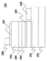
図2は、本実施の形態のLED素子104の構造を示した断面断面図である。本LED素子104は、サファイア基板201上に、GaNバッファ層(図示せず)と、n型のGaN層202、In0.2Ga0.8N活性層203、p型Al0.1Ga0.9N蒸発防止層204、p型Al0.1Ga0.9N上部蒸発防止層205、p型GaNコンタクト層206を順次積層されている。次に反応性イオンビームエッチング(RIBE)によってn型のGaN層202が露出するまでドライエッチングする。次にp型コンタクト層206上の一部にニッケル(Ni)膜207をパターン形成する。更にNi膜207上に金(Au)電極パッド208を形成し、次にn型GaN層202の露出した表面の一部にチタン(Ti)膜、更にその上にアルミ(Al)膜で構成されたn電極209を形成する。
【0021】
上記LED素子104は次のような工程で作製される。まず、MOCVD装置を用いてH2雰囲気中でサファイア基板201を1050℃で加熱し、サファイア基板の表面処理を行う。その後、基板温度を500℃まで下げ、GaNバッファ層(図示せず)を形成する。このとき、バッファ層の層厚は250Åとする。次に基板温度を1020℃まで上げてn型GaN層202を4μm程度成長させる。次に基板温度を720℃に下げ、ノンドープ又はSiドープIn0.2Ga0.8N活性層203を約30Åの膜厚で成長させる。次に基板温度をノンドープ又はSiドープIn0.2Ga0.8N活性層の成長温度と同じ720℃でp型Al0.1Ga0.9N蒸発防止層204を100Å成長する。次に基板温度を900℃に上げ、p型Al0.1Ga0.9N上部蒸発防止層205を100Å成長する。p型Al0.1Ga0.9N蒸発防止層204の成長温度はノンドープ又はSiドープIn0.2Ga0.8N活性層の成長温度と同一温度が望ましいが、実質的に同一であればよく、プラスマイナス50度程度は許容される。その後基板温度を1000℃としてp型GaNコンタクト層206を3000Å成長する。その後、n電極209を形成するため、レジストを塗付してフォトリソグラフィによりパターニングを行い、成長した半導体層の一部をドライエッチングにより除去してn型のGaN層202を露出させ、露出したn型のGaN層202の表面の一部にn電極209を形成する。次に、レジストを除去してフォトリソグラフィによりパターニングを行い、p型電極コンタクト層206上の一部にニッケル(Ni)金属膜207を30〜100Åの膜厚で蒸着する。また導電膜を形成したときと同様の手順で、導電膜上の一部に金(Au)パッド電極208を4000Åの厚さで形成する。
【0022】
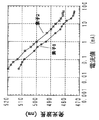
図3は、本実施の形態のLED素子104を直流駆動した場合の駆動電流値とその時の発光波長の関係を示す図である。ここで、発光波長とは、次のように定義している。図4に図示すように、LED素子104の発光波長スペクトルは単一のピークをもち、また、発光波長半値幅が30nm程度である色純度の良好な発光特性を示している。本実施の形態のLED素子104においては、発光色を、発光波長スペクトルのピーク波長をもって代表させることができ、本明細書ではこれを、発光波長と表現した。以下では、簡単のために、発光波長を発光色のパラメータとして用いることにする。図3において、素子1では、駆動電流が0.1mAのとき発光波長508nm(緑色)、駆動電流が1mAのとき発光波長494nm(青緑色)、駆動電流が10mAのとき発光波長481nm(青色)と、駆動電流を増加させるにつれて波長が短波長にシフトするブルーシフト現象が観測されている。すなわち、0.1mA駆動時に比べて10mA駆動時では20nm以上の短波長化が生じている。このように、20nm程度以上の短波長化は目視で観測する場合に異なる色として観測される。一般に、目視での観測において色を同一に保つためには、可視光のいずれの波長域のLED素子であっても電流値変化に対する波長の変化を6nmより小さく抑制することが必要である。
【0023】
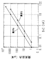
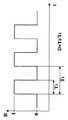
図5は、本実施の形態のLED素子104をパルス駆動した場合の発光出力特性を示す図である。横軸は、方形波パルス電流RのデューティDと、電流値Iとの積D×I(単位mA)とし、縦軸を発光出力P(単位μW)とした。本明細書では、パルスとは周期的なパルスのことを表わしており、これを図6に示している。図6を参照して、電流値Iとはパルスの電流値(波高値)であり、デューティDは、パルスの周期T1とパルス幅T2とからD=T2/T1で定義される。よって、デューティDと、電流値Iとの積D×Iは、LED素子に注入される電流の時間平均値(平均電流)である。本実施の形態では、本発明の原理をわかりやすく説明するために、発光出力が電流値にほぼ比例するような電流領域における駆動を想定している。このとき、LED素子に注入される平均電流に比例してLED素子の発光出力(時間平均とする)が得られ、図5のグラフのように直線で表わされる特性となっている。つまり、発光出力PはほぼP∝D×Iと考えることができる。ここで、LED素子を人が観察したときにちらつきを感じないことが望ましいことから、周期T1は30ms以下であればよく、特に10ms以下とすることが望ましい。またパルス幅T2は発光素子の活性層におけるキャリアの再結合寿命と同等かそれより長いほうが望ましく、InGaN活性層を有する発光素子ではパルス幅は0.2ns以上、より好ましくは1ns以上に設定される。
【0024】
以下に、図1ないし図6を参照して、本実施の形態のLED装置の動作の詳細を説明する。ここでは、図3および図5に素子1として記載されているLED素子を発光波長490nm(青緑色)、発光出力100μWで発光させる場合を例にとって説明する。このように、発光強度のパラメタとしては、発光出力を用いた。このとき、LED点灯回路1には、外部より、LEDの発光波長が490nmであることを指示する色信号c=c490と、LEDの発光出力が100μWであることを指示する強度信号p=p100が入力される。
【0025】
次に、本実施形態装置の動作について説明する。先ず、外部から色信号cが色信号−電流値信号変換部102に入力されると、ここでは、図3(素子1)に示される駆動電流値対発光波長特性にしたがって、色信号cから電流値信号iへの変換が行われる。本例の色信号c=c490が入力された場合、図3(素子1)の駆動電流値対発光波長特性によれば発光波長490nmに対応する電流値は2mAであり、方形波パルス発生部103の出力すべきパルスの電流値Iが2mAであることを指示する電流値信号i=i2を発生し、演算処理部101と方形波パルス発生部103に送る。
【0026】
次に、演算処理部101では、強度信号pと上記電流値信号iが入力されるので、図5(素子1)に示されるような電流値IとデューティDの積対発光出力特性の関係から、デューティDが演算される。ここで強度信号としてp100、電流値信号としては上記i2が与えられており、図5(素子1)よりP=100μWに対応する電流値IとデューティDの積D×Iは1mAであり、また、電流値信号の指示する電流値は2mAであることから、D=0.5が算出される。これにより、方形波パルス発生部103の出力すべきパルスのデューティDが0.5であることを指示するデューティ信号d=d0.5を発生し、方形波パルス発生部103に送る。
【0027】
方形波パルス発生部103では、色信号−電流値信号変換部102から送られてきた電流値信号i=i2と演算処理部101から送られてきたデューティ信号d=d0.5に従って、電流I=2mA、デューティD=0.5のパルス電流Rを発生し、出力する。このパルス電流RによりLED素子104が駆動され発光する。以上のような、手順を踏むことにより、駆動電流値に対して発光波長依存性のあるLED素子を用いても、指示された発光波長と発光出力で発光させることができた。
【0028】
次に、図3および図5において、素子2として記載されているLED素子を上記と同一の発光出力100μW、発光波長490nmで発光させる場合について説明する。図3に示される駆動電流値対発光波長特性のように、素子2では素子1との特性のばらつきのため、各電流値における発光波長が約6nm程度長波長側にシフトしている。また、図5に示されるように、電流値IとデューティDの積対発光出力特性の関係も、素子1の場合と異なり、低出力側にシフトしている。
【0029】
色信号c=c490が色信号−電流値信号変換部102に入力され、図3(素子2)の駆動電流値対発光波長特性図から発光波長490nmに対応した電流値5mAを指示する電流値信号i=i5を発生し、演算処理部101とパルス発生部103に転送される。
【0030】
演算処理部101では、強度信号pとしてp100、電流値信号としては上記i5が与えられており、図5(素子2)の電流値IとデューティDの積対発光出力特性の関係からP=100μWに対応する電流値IとデューティDの積D×Iは3であり、また、電流値信号の指示する電流値は5mAであることから、D=0.6が算出される。これにより、パルス発生部103の出力すべきパルスのデューティDが0.6であることを指示するデューティ信号d=d0.6を発生し、パルス発生部103に送る。
【0031】
パルス発生部103では、色信号−電流値信号変換部102から送られてきた電流値信号i=i5と演算処理部101から送られてきたデューティ信号d=d0.6に従って、電流値5mA、デューティ0.6のパルス電流Rを発生し、出力する。このパルス電流RによりLED素子104が駆動され、上記指定の発光出力と発光波長で発光した。
【0032】
このように、本発明の駆動方法を取ることで、複数の特性のバラツキのある電流値により発光波長の変化するLED素子においても同一波長、同一出力で駆動することができた。駆動電流値により発光波長の変化するLED素子においては、所定の電流値でLED素子を駆動すると、発光波長がそれぞれ特性のバラツキにより異なる、すなわち、色調が異なるという問題が生じていたが、本発明により、この問題が解決された。つまり、演算処理部101には、図5に示す電流値Iと、デューティDの積対発光出力の関係をテーブル形式や関数として記録させておけば良く、また、色信号−電流値信号変換部102には、図3に示す各々駆動したい素子に対応した電流値対発光波長のデータをテーブル形式や関数として記録させておけばよい。
【0033】
なお、上述の実施の形態としてパルス波形は方形波としたが、パルス発生部で発生するパルス波形は方形波以外、三角波等その形状は問題とならず、どのような形態であっても良い。また、パルス波の発生形態としては以下に記述するような方法も適用可能であった。周期を一定として、パルスの幅を変化させてデューティを変化させた場合。パルスの幅を一定として、周期を変化させてデューティを変化させた場合。ある一定時間内のパルス数を変化させデューティを変化させた場合。更に、図18(a)に示すようにパルスが一定周期の前半側に集中したもの、(b)のようにパルスが一定周期の後半側に集中したもの、(c)のように一定周期の全体に広がって発生したような場合も考えられる。すなわち、駆動電流の平均電力が一定となるように、個々のパルスの形や幅、個数等は回路構成での容易な方法に従い、任意に選択することができる。以上のようにパルスの発生形態には様々なバリエーションがあるが、これ以外の発生形態であっても本発明において何ら問題とならず適応可能である。
【0034】
(実施の形態2)
本実施の形態では、実施の形態1(素子1)において、LED点灯回路に指示する発光強度の指示を、50μW、100μW、200μWと時間的に変化させ、かつ、発光波長の指示を実施の形態1と同じ490nmと一定にした場合について説明する。この場合、色信号cはc=c490で一定であり、強度信号pがそれぞれ指示された発光強度に応じて、p=p50、p100、p200と変化し入力されるものとする。
【0035】
色信号cはc=c490で一定であるから、色信号−電流値信号変換部102の出力する電流値信号iは実施の形態1と同じであり、i=i2である。
【0036】
演算処理部101の出力するデューティ信号dは、実施の形態1と同じ手順にしたがって演算され、強度信号pは、p=p50、p100、p200と変化するにしたがって、結果が、D=0.25、0.5、1となるから、それぞれの指示するデューティ信号d=d0.25、d0.5、d1を順次パルス発生部103におくる。
【0037】
これにより、実施の形態1と同様の手順により、外部より入力された、上述の時間変化する発光強度および一定の発光波長である指示通りに、LED素子104が発光した。(但し、この場合200μW以上は出せない。)
本実施の形態においては、駆動電流値によって発光波長(色調)の異なるLED素子を用いたにもかかわらず、発光波長(色調)を指定された一定に保持したまま、発光強度のみを変化させることができた。
【0038】
このような駆動方法は、他の発光色のLED素子と同時に点灯して色調を表現するような表示装置に応用すれば、色ずれを抑制することができ、また、LED素子により蛍光体を励起発光させるような表示装置に応用すれば、励起波長ずれによる発光効率の低下や、色調ずれを防止することができ、効果が非常に高い。ここで説明に用いた素子とは、特性の異なるLED素子を(特性にバラツキのある素子)を用いても実施の形態1に示したのと同様の方法、理由により、所定の発光色で発光強度のみを変化させることができた。
【0039】
(実施の形態3)
本実施の形態では、実施の形態1におけるLED点灯回路を簡略化した形を示す。この場合のLED点灯回路は図7に示すように、方形波パルス発生部103aのみから構成されており、LED点灯回路の外部から与えられる信号も強度信号pのみである。方形波パルス発生部103aでは、光出力に対応する強度信号pの値に基づいて、LED素子104に流す電流パルスのデューティーのみを変化させ、電流波高値はあらかじめ設定したほぼ一定の値とした。ここで波高値がほぼ一定と見なせる範囲としては、当該回路の接続されたLED素子の波長変化(ブルーシフト)が6nm以下の範囲に収まるように制御されていれば、多少の電流波高値の異なりは問題とはならず、ここで言う“一定”の範疇に包含されている。この場合の電流波高値の設定電流をLED素子の信頼性が確保できる範囲の最大値に設定することで、表示の発光強度のダイナミックレンジを最大とできるので最も望ましい。具体的には、この場合のパルス波高値として10mA以上300mA以下に設定することが望ましい。
【0040】
このような簡易の点灯回路の構成であっても、接続されたLED素子から発光される光の波長を観測した所、パルスデューティーが0.2%から100%まで変化させ、その時の光出力と波長を観測した結果、0.1mW〜50mWまでの光出力変化がみられたが、この範囲内での発光波長の変化は472nmから468nmへの4nm程度の変化であり、色変化として目に感じられる6nmを下回っていた。よって、色信号cを用いる実施の形態1のような演算処理部101や色信号−電流値信号変換部102による色制御を実施しない場合においても、LED素子104に印加される駆動パルスの電流波形が接続されたLED素子104の波長変化(ブルーシフト)が6nmの範囲内となるようにパルス波高値をほぼ一定に制御し、パルスデューティーを主として変化させて光出力を制御する方法を採用することで、LED素子104のブルーシフトに基づくLED素子の色変化を顕著に抑制することができ、実用上、色変化が感知できない範囲にまで改善できた。
【0041】
この場合のあらかじめ駆動回路で設定される電流値としては、LED素子の信頼性に支障の無い範囲で最大の電流パルス波高値と設定することにより、光出力のダイナミックレンジを最も大きくすることができる。
【0042】
(実施の形態4)
本実施の形態では、実施の形態1(素子1)において、LED点灯回路に指示する発光波長の指示を、475nm(青色)、485nm(青〜青緑色)、494nm(青緑〜緑色)と時間的に変化させ、かつ、発光強度の指示を60μW一定にした場合について説明する。この場合、強度信号pは、p=p60で一定であり、色信号cがそれぞれ指示された発光強度に応じてc=c475、c485、c49 4と変化し入力されるものとする。
【0043】
色信号−電流値信号変換部102の出力する電流信号は、実施の形態1と同様に素子1の場合は図3に従って変換されて、色信号c=c475、c485、c494に対して、それぞれ電流値30mA、4mA、1mAを指示する電流値信号i=i30、i4、i1を出力する。
【0044】
演算処理部の出力するデューティ信号は、実施の形態1と同じ手順にしたがって演算され、i=i30、i4、i1と変化するにしたがって、結果が、D=0.02、0.15、0.6となるから、それぞれの指示するデューティ信号d=d0.02、d0.15、d0.6をパルス発生部103におくる。
【0045】
これにより、実施の形態1と同様の手順により、外部より入力された、上述の時間変化する発光波長および一定の発光強度である指示通りに、LED素子104が発光した。
【0046】
本発明の駆動方法を用いると一つのLED素子で光強度を変えず、発光色を変化させることができた。このように、本実施の形態の方法にしたがって発光色を変化させる場合には、電流値を10倍以上変化させることが色調の変化のためには望ましく、特に、20倍以上変化させることが望ましかった。
【0047】
このような駆動方法は、表示装置に応用すれば、単一のLED素子で光強度を変えずに発光波長を変化させるので、視覚効果の高い表示装置を簡単な構成で実現できる。LED点灯回路に入力する色信号を連続的に変化させて、発光色を連続的に変化させるようなことも、容易にできる。
【0048】
また実施の形態2、3を組み合わせることにより、素子1において、490nmで200μW、475nmで60μWと任意の異なる発光波長で、異なる発光強度で発光させることも可能となる。
【0049】
以上、実施の形態1から4においては、原理の説明をわかりやすくするために、電流値と発光出力との関係が比例関係をもったLED素子として、動作を説明してきたが、本発明はこれに限られるものではない。実際のLED素子では比例関係を持っていない場合も多いのである。図8はこのようなLED素子の電流値対発光出力(瞬間値)特性を示す図であり、比例関係にないことから、グラフが曲線になっている。このような、LED素子について、図5のようなD×I対発光出力特性のグラフを描こうとすると、グラフを一本の線で描くことができずに、電流値Iの値ごとに異なるラインを描かなければならない。
【0050】
図8に示される素子の場合で、実施の形態1と同条件の発光波長490nm、発光出力100μWで光らせようとした場合を実施の形態1と同様に考える。ただし、この素子の電流値対発光波長特性は図3(素子1)と同じとする。色信号c=c490が色信号−電流値信号変換部102に転送され、実施の形態1と同じく電流値信号i=i2(電流値2mAを指示)を出力する。図8によれば、電流値2mAのとき、300μW(瞬間値)の光を出力するから、演算処理部101では、100μW/300μW=1/3のデューティDを演算し、これに応じたデューティ信号dを出力すべきである。ここで基本的には、デューティDと発光出力Pとの間に比例関係があると考えたが、LED素子の放熱が十分でない場合には、デューティDと、電流値Iとの積D×Iの値が大きくなると発熱により発光効率が低下するので必ずしも成り立つものではない。要は、発光出力Pが、デューティDと電流値Iを変数とする関数(あるいは、DはPとIを変数とする関数)であり、これは、あらかじめLED素子の特性を測定することにより得ることができ、演算処理部は、LED素子に応じてこの関数を計算し所要のデューティ信号dを出力するものとすればよい。あるいは発光出力Pと、デューティDと電流値Iの関係をテーブルとして記録しておいてもよい。この様に、本発明の駆動方法は、電流値対光強度特性が線形でない素子に対しても駆動することができるものである。
【0051】
また、実施の形態1ないし4においては、実施の形態1の中で説明したように、発光スペクトルのピーク値をパラメタとして発光色を表現してきた。これは、単に説明の簡単化のために用いたものであり、実施の形態1から4で説明した本発明の本質に係わるものではない。例えば、CIE標準色度図の座標等を用いて表現しても、発明の本質が変化するものではない。
【0052】
またさらに、実施の形態1ないし4においては、簡単のために、LED素子の発光強度を発光出力(単位W)を用いて表わしてきたが、他のパラメタを用いてもよい。特に、輝度(単位cd/m2)、光度(単位cd)、光度パワー(単位lm)のように、視感度を考慮したパラメタを用いれば、実施の形態4の場合のように、光強度を一定にして波長のみを変化させるような駆動を行う場合、波長が変化することによる見ための明るさの変化がなくなり、好都合である。ただし、この場合、図5において、発光波長すなわち電流値Iにより、光強度が変化するので、デューティDと、電流値Iとの積D×I対発光出力(パワー)の関係を一本の直線で表現することは不可能になる。しかしながら、上述のごとく本発明の駆動方法は、電流値対発光出力特性が線形でない素子に対しても駆動することができるものであり、このような変更は、演算処理部に保持する発光出力PとデューティDと電流値Iとの関係を、実施の形態1ないし4の場合とは発光出力Pの単位を変えて保持すれば実現でき、実施の形態1から4で説明した本発明の本質に係わるものではない。
【0053】
また、実施の形態1ないし4においては、特定のLED素子(素子1、素子2)を用いて説明したが、これは、電流増加につれて波長が短くなる(駆動回路で設定される最小駆動電流と最大駆動電流での波長差が6nm以上のブルーシフトを生ずる)全てのLED素子を対象とすることができる。例えば、図2に示したLED素子とほとんど同じ構成で、InGaN活性層の組成を変更することで、電流値を0.1mAから100mAまで変えたときに、発光波長が590nmから530nmまで変化するものを作製することができた。さらに、導電性(望ましくはn型)GaN基板上に作製されたInGaN活性層やInGaAlN活性層を有するLED素子もこの対象であることは言うまでもない。このようなLED素子を用いたときには、実施の形態1ないし4と同様の構成にて、橙〜黄〜黄緑〜緑色の内の所定の発光色と発光強度で発光するLED素子を実現できた。
【0054】
(実施の形態5)
図9は本実施の形態のLEDランプを示す図である。本実施の形態のLEDランプは、駆動電流値により発光色が変化するLED素子801と、その前面に設けられた蛍光体802とから構成される。LED素子801の発光出力と蛍光体802の発光出力が混合されて出力される。ここで、LED素子801は実施の形態1に示されたものと同じである。
【0055】
以下に、本実施の形態のLEDランプの動作について説明する。図10は、蛍光体802が460nmで励起されたときの励起スペクトルおよび発光スペクトルを示した図である。本実施の形態に使用される蛍光体の励起スペクトルのピークは、460nm程度にあり、この波長の光を照射されたときに、最も効率よく発光スペクトルに示される蛍光を生じることが示されている。本例では発光のピークは630nmであり、赤色の発光を示している。このような特性の蛍光体として、例えばYAG系蛍光体がある。
【0056】
このような蛍光体802に図3(素子1)に示される電流値対発光波長特性をもつLED素子で励起することを考える。素子1は、駆動電流値が0.1〜2〜30mAと変化するに従って、発光波長が、508(緑色)〜490(青緑色)〜474nm(青色)と変化する。図11はCIE標準色度図であり、図中の素子1と示したラインが0.1〜2〜30mAのように電流値を変化させたときの素子1の発光色の軌跡を示している。また、図11の蛍光体と記した点は、図10に示される蛍光体の発光スペクトルにより求められた蛍光体の発光色を示す点である。ここで、図10に示される蛍光体の励起スペクトルによれば、素子1の発光波長が508nmのときは素子1の駆動電流が小さいので発光出力が小さく、かつ励起スペクトルの端にあるため、蛍光体はほとんど励起されない。しかし、素子1の発光波長が474nmのときは駆動電流が大きく発光出力が大きくなり、かつ励起スペクトルのピーク付近にあるため、強く励起され発光することになる。このように、素子1の発光波長が短波長になるにしたがって、蛍光体は強く励起される。
【0057】
例えば、本実施の形態のLEDランプにおいて、LED素子801を0.1mAで駆動したとき、LED素子801が発光して508nmの出力が得られるが、蛍光体はほとんど励起されないので、LEDランプはほぼLED素子801の発光のみが出力されて緑色になる。LED素子801を30mAで駆動したとき、LED素子の発光(青色474nm)と、このLED素子の発光によって励起される蛍光体802の発光(赤色630nm)とが混合するので、赤紫色になる。また、LED素子801を2mAで駆動したときには、490nm(青緑色)の発光波長が得られるが、発光出力はそれほど強くなく、かつ励起スペクトルの端近くにあるため蛍光体802の発光はそれほど強くなく、LED素子801の発光(青緑色490nm)と混合されて、白色になる。電流値を0.1〜2〜30mAと変化させたときの、このような、LEDランプ発光色のCIE標準色度座標における軌跡は、図11で「実施の形態4のLEDランプ」と記入されたラインのようになる。このように、本実施の形態のLEDランプは、電流値を0.1〜2〜30mAと変化させたとき、緑〜白〜赤紫色と順に変化する。
【0058】
このように、本実施の形態によれば、電流値により発光色が変化するLED素子と蛍光体とを組み合わせることにより、電流値による発光色の変化を単にLED素子のみを用いただけでは実現できないLEDランプを得ることができた。ここでは、蛍光体として、図10に示す特定のものを用いて説明したが、蛍光体の種類は多岐にわたるので、適宜LED素子と蛍光体との組み合わせを設定することで電流値による発光色の変化をバリエーションを極めて豊かにすることが可能である。
【0059】
(実施の形態6)
本実施の形態のLEDランプは、図9と同様に、駆動電流値により発光色が変化するLED素子801と、その前面に設けられた蛍光体802とから構成される。LED素子801の発光出力と蛍光体802の発光出力が混合されて出力される。以下に、本実施の形態のLEDランプの動作について説明する。
【0060】
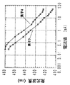
図12は、本実施の形態のLED素子の電流値対発光波長特性を示す図である。素子3は、電流値が0.1〜2〜30mAと変化するに従って、発光波長が、450nm(青色)〜430nm(青色)〜415nm(青紫色)と変化する。このような素子3は、実施の形態1および図2に示したLED素子において、InGaN活性層の組成を変更することにより製造できる。図13はCIE1960UCS色度図であり、その色度座標(u、v)は、CIE標準色度図における色度座標(x、y)と、u=4x/(−2x+12y+3)、v=6y/(−2x+12y+3)の関係がある。UCS色度図においては、異なる2色の座標点の距離が視覚的に感じる色の差に対応しているという特徴がある。本図においてLED素子と記載しているラインが、本実施の形態のLED素子を0.1から30mAまで変化させたときの発光色の変化をしめす軌跡である。このとき、(u、v)=(0.25、0.03)〜(0.19、0.06)程度まで変化している。よって座標間の距離(色差)は、0.07程度である。
【0061】
また、図14は、本実施の形態の蛍光体の励起および発光スペクトルを示した図である。本図の範囲で、励起スペクトルのピークは、430nm程度にあり、この波長の光を照射されたときに、最も効率よく発光スペクトルに示される蛍光を生じることが示されている。本例では発光のピークは650nmであり、赤色の発光を示している。このような、励起および発光スペクトルは、6MgO・As2O5:Mn4+系の蛍光体材料により実現できる。図13において、蛍光体と記してある点(u、v)=(0.55、0.31)が、本蛍光体の発光色を示している。
【0062】
ここで、図14に示される蛍光体の励起スペクトルによれば、素子3の発光波長が450nm(0.1mA)のときはLED素子の発光出力が小さく、蛍光体はほとんど励起されない。しかし素子3の発光波長が415nm(30mA)と短波長になるにしたがって、LED素子の発光出力が強くなるとともに蛍光体の励起スペクトルのピーク付近にあるため、強く励起され発光することになる。したがって、LEDランプから発する光は、LED素子を0.1mAで駆動したとき、ほぼLED素子の発光が優勢で青色になり、LED素子を30mAで駆動したとき、蛍光体の発光(赤色660nm)とLED素子の発光(青紫色415nm)とが混合するが、LED素子の発光色について視感度が低いため、蛍光体の発光(赤色660nm)が優勢に感じられ、赤色になる。また、素子3を2mAで駆動したときには、素子3の発光波長は青色430nmであり、LED素子の発光出力がそれほど強いとともに、蛍光体の発光もそれほど強くなく、LED素子の発光(青色430nm)と混合されて紫色になる。
【0063】
このように、電流値を0.1〜2〜30mAと変化させたときの、LEDランプの発光色のUCS色度図における軌跡は、図13で「LEDランプ」と記入されたラインのようになる。このとき、LEDランプの色調は(u、v)=(0.25、0.1)〜(0.53、0.28)程度まで変化しており、座標間の距離(色差)は、0.33程度である。このように、電流値を変調したとき、本実施の形態に用いられたLED素子よりも、本実施のLEDランプは大きく色調を変化させる。これは、蛍光体として、LED素子の発光波長の変化にしたがって、大きく(2倍以上、好ましくは5倍以上)励起効率を変えるような蛍光体を選定したことにもとづく。
【0064】
このように、本実施の形態によれば、電流値により発光色が変化するLED素子と、LED素子の発光波長の変化にしたがって、大きく励起効率を変えるような蛍光体を選定したことにもとづく蛍光体とを組み合わせることにより、電流値によるLED素子の発光色の変化よりも大きい変化が得られるLEDランプが得られた。
【0065】
(実施の形態7)
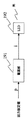
上記実施の形態5で示したLEDランプを上記実施の形態1で説明したLED点灯回路により駆動した場合に関して説明する。LED点灯回路の基本構成は図1に示した回路と同じであるが、改めて図17に示している。異なる点はLED素子164が実施の形態5に示したように、蛍光体をLED素子の前面に持つLEDランプである点である。また、この図17の場合、LED点灯回路16には、外部よりLEDランプの発光強度を指示する輝度信号kとLED発光色を指示する色度信号uとが入力され、LED素子164を駆動する、電流値I、デューティDのパルス電流Rを出力する。上記LED点灯回路16は、入力される色度信号uを電流値信号iに変換して出力する、色度信号−電流値信号変換部162と、輝度信号kと、電流値Iを指示する電流値信号iとから、デューティDを指示するデューティ信号dを演算して出力する演算処理部161と、入力される電流値信号iとデューティ信号dの指示に応じて、それぞれ、電流値I、デューティDのパルス電流をLED駆動電流として出力するパルス発生部163とから構成される。
【0066】
図16は、本実施の形態のLED素子164の駆動電流対色度(u値)特性を示す図である。ここで、u値とは、次のように定義している。実施の形態1において図4を用いて述べた発光波長スペクトルのピーク波長から求めた値からUSC色度図でu軸の値を算出し、その値をu値としている。従って、以下では、簡単のために、u値を発光色のパラメタとして用いることにする。
【0067】
ここで、図10に示される蛍光体の励起スペクトルによれば、励起波長が508nm(0.1mA)のときはほとんど蛍光体は励起されず、474nm(30mA)と短波長になるにしたがって、強く励起され発光することになる。したがって、LED装置から発する光は、LED素子を0.1mAで駆動したとき、ほぼLED素子の発光が優勢で青色になり、LED素子を30mAで駆動したとき、蛍光体の発光(赤色660nm)とLED素子の発光(青紫色415nm)とが混合するが、LEDの発光色について視感度が低いため、蛍光体の発光(赤色660nm)が優勢に感じられ、赤色になる。また、2mAで駆動したときには、蛍光の発光はそれほど強くなくLED素子の発光(青色430nm)と混合されて、紫色になる。電流値を0.1〜2〜30mAと変化させたときの、このような、LEDランプ発光色のUCS色度図における軌跡は、図13で「LEDランプ」と記入されたラインのようになる。
【0068】
よって電流値とu値の関係をグラフに示すと図16のようになる。ここで図16において、駆動電流が0.1mAのときu値=u0.25、駆動電流が1mAのときu値=u0.37、駆動電流が10mAのときu値=u0.475と、駆動電流により変化していることがわかる。
【0069】
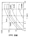
さらに、図15は、本実施の形態のLEDランプの輝度特性を示す図である。横軸は、方形波パルス電流Rの電流値Iとし、縦軸を輝度(単位mcd)とした。各デューティDの値に対して特性を示す曲線を描いた。すなわち、本図は本実施の形態のLEDランプの輝度L、電流値Iの関係を示す図である。なお、本発明に用いるパルス周期T2は特に規定しないが、発光を観察したときにちらつきを感じないことが望ましいことから、周期T2は、30ms以下であればよく、特に、10ms以下とすることが望ましい。
【0070】
以下に、図14、15、16、17を参照して、本実施の形態のLED装置・LED点灯回路の動作の詳細を説明する。ここでは、図15および図14に記載されているLED素子をu値=u0.37、発光強度100mcdで発光させる場合を例にとって説明する。このように、発光強度のパラメタとしては、輝度を用いた。このとき、LED点灯回路16には、外部より、色度信号u=u0.37と、LEDの輝度が100mcdであることを指示する輝度信号k=k100が入力される。
【0071】
先ず、外部から色度信号uが色度信号−電流値信号変換部162に入力される。ここでは、図16に示される駆動電流対色度特性にしたがって、色度信号uから電流値信号iへの変換が行われる。本例の色信号が入力されたとすると、図16の電流値対色度特性によれば色度信号0.37に対応する電流値は1mAという事になり、パルス発生部163の出力すべきパルスの電流値Iが1mAであることを指示する電流値信号i=i1を発生し、演算処理部161とパルス発生部163に送る。
【0072】
次に、演算処理部161には、輝度信号kと上記電流値信号iが入力される。演算処理部161では、図15に示されるようなLEDランプの輝度特性の関係から、デューティDが演算される。ここで輝度としてk100、電流値信号としては上記i1が与えられており、図15よりk=100μWに対応するデューティDはIは0.5でありD=0.5が算出される。これにより、パルス発生部163の出力すべきパルスのデューティDが0.5であることをを指示するデューティ信号d=d0.5を発生し、パルス発生部163に送る。
【0073】
それから、パルス発生部163では、色度信号−電流値信号変換部162から送られてきた電流値信号i=i1と演算処理部161から送られてきたデューティ信号d=d0.5に従って、電流値1mA、デューティ0.5のパルス電流Rを発生し、出力する。このパルス電流RによりLED素子164が駆動され、発光する。以上のような、手順を踏むことにより、駆動電流値に対して色度特性のu値依存性のあるLED素子を用いても、指示された輝度とUSC色度図のu値で発光させることができた。
【0074】
次に、図15および16において、説明に用いた素子と異なる素子(特性にバラツキのある素子)に対しても、実施の形態1で説明したように、同様の理由から所定の輝度と色度で発光させることが可能である。
【0075】
(実施の形態8)
本実施の形態では、実施の形態7において、LED点灯回路に指示する輝度の指示を、10、40、100mcdと時間的に変化させ、かつ、色度特性のu値の指示を実施の形態7と同じ0.37と一定にした場合について説明する。
【0076】
この場合、色度信号uはu=u0.37で一定であり、輝度信号kがそれぞれ指示された発光強度に応じて、k=k10、k40、k100と変化し入力されるものとする。
【0077】
色度信号−電流値信号変換部162の出力する電流信号は実施の形態6と同じであり、i=i1である。
【0078】
演算処理部161の出力するデューティ信号は、実施の形態6と同じ手順にしたがって演算され、k=k10、k40、k100と変化するにしたがって、結果が、D=0.02、0.1、0.42となるから、それぞれの指示するデューティ信号d=d0.02、d0.1、d0.42をパルス発生部163におくる。
【0079】
これにより、実施の形態6と同様の手順により、外部より入力された、上述の、時間変化する輝度および一定の色度特性(u値)を指示通りに、LED素子164を駆動した。(但し、この場合180mcd以上は出せない。)
本実施の形態においては、駆動電流値によって発光波長(色調)の異なるLED素子を用いたにもかかわらず、発光波長(色調)を指定された一定に保持したまま、発光強度のみを変化させることができた。ここで説明に用いた素子とは、特性の異なるLED素子を(特性にバラツキのある素子)を用いても実施の形態1に示したのと同様の方法、理由により、所定の発光色で発光強度のみを変化させることができた。
【0080】
このような駆動方法は、他の発光色のLED素子と同時に点灯して色調を表現するような表示装置に応用すれば、色ずれを抑制することができ効果が非常に高い。
【0081】
(実施の形態9)
本実施の形態では、実施の形態7において、LED点灯回路に指示する色度特性のu値の指示を、0.25、0.37、0.51と時間的に変化させ、かつ、輝度の指示を40mcd一定にした場合について説明する。
【0082】
この場合、輝度信号は、k=k60で一定であり、色度信号uがそれぞれ指示された発光に応じてu=u0.25、u0.37、u0.51と変化し入力されるものとする。
【0083】
色度信号−電流値信号変換部162の出力する電流信号は、実施の形態7と同様に図16に従って変換されて、色度信号u=u0.25、u0.37、u0.51に対して、それぞれ電流値0.01mA、1mA、20mAを指示する電流値信号i=i0.01、i1、i20を出力する。
【0084】
演算処理部161の出力するデューティ信号は、実施の形態7と同じ手順にしたがって演算され、i=i0.01、i1、i20と変化するにしたがって、結果が、D=1、0.22、0.1となるから、それぞれの指示するデューティ信号d=d1、d0.22、d0.1をパルス発生部163におくる。
【0085】
これにより、実施の形態6と同様の手順により、外部より入力された、上述の、時間変化するu値および一定の輝度である指示通りに、LED素子164が発光した。
【0086】
本発明の駆動方法を用いると一つのLED素子で輝度を変えず、発光色を変化させることができた。このように、本実施の形態の方法にしたがって発光色を変化させる場合には、電流値を10倍以上変化させることが色調の変化のためには望ましく、特に、20倍以上変化させることが望ましかった。
【0087】
このような駆動方法は、表示装置に応用すれば、単一のLEDランプで輝度を変えずに色度特性のu値を変化させるので、人間の目にはどの波長の光も同じ明るさで感じられ、視覚効果の高い表示装置を簡単な構成で実現できる。LED点灯回路に入力する色信号を連続的に変化させて、発光色を連続的に変化させるようなことも、容易にできる。
【0088】
また、本実施例では、蛍光体を励起して発光するLED素子を用い、更に実施の形態1で説明したLED駆動回路および駆動方法により1つのLED素子で、電流値を変化させることにより、輝度を変化させること無く、青色〜赤色まで発光が実現できた。これまでの素子では得られない程大きな発光色の変化である。
【0089】
実施の形態1〜9において、LED素子の駆動電流を周期的なパルスの場合で説明したが、発光を観察したときちらつきを感じないことが望ましいため、駆動電流の基本周期は30ms以下であれば良く、特に10ns以下とすることが望ましい。また、個々のパルスの幅は前述のように0.2ns以上、より望ましくは1ns以上とすることで活性層中でのキャリア濃度を確実に制御することが可能となる。
【0090】
また、実施の形態1〜9において、電流値を一定として、デューティを変化させる、もしくはデューティを一定として電流値を変化させ発光強度と波長を変化させているが、発光色の色目が変化しない程度(所望波長の±3nm以下)であれば電流値、もしくはデューティを所望の波長の±3nm以下に発光波長がなるように変化させてもかまわない。実施の形態5〜9において、蛍光体は所要とする励起スペクトルと発光スペクトルの組み合わせに応じて適当に選択することができる。例えば、赤色発光の蛍光体として、ZnS:Cu、LiAlO2:Fe3+、Al2O3:Cr、Y2O3:Eu3+、Y(P,V)O4:Eu3+、Y2O3:Eu蛍光体、Y2O3:Eu蛍光体とY2O3S:Eu蛍光体との混合体、だいだい色発光の蛍光体として、ZnS:Cu,Mn、(Zn,Cd)S:Ag、ZnS:Mn、(Sr,Mg,Ba)3(PO4)2、緑色発光の蛍光体として、ZnS:Cu、Al、LaPO4:Ce3+Tb3+、Sr(S,Se):Sm,Ce、ZnSiO4:Mn2+、βZnS:Cu、ZnS:Cu,Fe(Co)、ZnS:PbZnS:Cu蛍光体、ZnS:Cu,Al蛍光体とY2Al5O12:Tb蛍光体の混合体、青色発光の蛍光体として、CaS:Bi、(Sr,Ca)10(PO4)6Cl2:Eu2+、SrS:Sm,Ce、Sr2P2O7:Eu2+、βZnS:Ag、(Ba,Ca,Mg)10(PO4)6Cl:Eu2+、3Sr3(PO4)2・CaCl2:Eu2+蛍光体、白色発光の蛍光体として、ZnO:Zn、ZnS:AsZnS:Au,Ag,Al、Ca2P2O7:Dy、Ca3(PO4)2・CaF2:Sb、3Ca3(PO4)2・Ca(F,Cl)2:Sb3+、3Ca3(PO4)2・Ca(F,Cl)2:Sb3+,Mn2+、MgWO4、3Ca3(PO4)2・Ca(F,Cl)2:Sb3+,Mn2+蛍光体を用いる。
【0091】
(実施の形態10)
上記実施の形態で記述してきたLED駆動方法、もしくはLED装置を用いて表示装置(ディスプレイ等)を実現できる。図19は上記で示したLED点灯回路、もしくはLED点灯方法を用いて作製されたディスプレイの概略図である。171はディスプレイ本体であり、この中に上記実施の形態で記述してきたLED点灯回路が組み込まれている。しかし、点灯回路をディスプレイに組み込まず点灯回路とディスプレイを分離し動作させても良い。
【0092】
図19において、LED素子もしくはLEDランプ172は、X方向、Y方向にマトリックス状に平面に配置されている。これら多くのLED素子、LEDランプを一度に所望の発光色、明るさで表示しようとするため、従来例で示したLED駆動回路で駆動した場合、各々のLED素子、LEDランプの特性のバラツキが大きく、発光色、明るさがばらついてしまい、ディスプレイの画質等の低下を招く。しかし、本発明の上記実施の形態1〜9で記述してきたLED装置、もしくはLED駆動方法を用いて図19の表示装置(ディスプレイ等)を作製した場合、実施の形態1、3または7で記述したように各LED素子、LEDランプにそれぞれ点灯回路を接続して駆動することにより、特性のばらついた複数のLED素子、LEDランプでも所望の発光色、明るさで発光させることができるため、ディスプレイの表示画像の画質を向上させることができる。
【0093】
【発明の効果】
本発明は、駆動電流値により発光色が変化するLED素子において、光強度を変化させても発光色が変化しないLED装置を実現できた。
【0094】
複数の、特性のバラツキのある電流値により発光色の変化するLED素子においても同一波長、同一光強度で駆動することができた。駆動電流により発光波長の変化するLED素子においては、所定の電流値でLED素子を駆動すると、発光波長がそれぞれ特性のバラツキにより異なる、すなわち、色調が異なるという問題が生じていたが、本発明により、この問題が解決された。
【図面の簡単な説明】
【図1】本発明の実施の形態1に関わるLED装置の概略図である。
【図2】本発明の実施の形態1に関わるLED素子の構造概略図である。
【図3】LED素子の電流値対発光波長特性図である。
【図4】LED素子の発光波長スペクトルである。
【図5】本発明のLED点灯回路で駆動されるLED素子の駆動電流値対デューティの積対発光出力特性図である。
【図6】本発明のLED点灯回路でパルス発生部で発生したパルス信号の概略図である。
【図7】本発明の実施の形態3に関わるLED装置の概略図である。
【図8】本発明のLED点灯回路で駆動されるLED素子の電流値対発光出力特性図である。
【図9】本発明の実施の形態5に関わるLEDランプの構造概略図である。
【図10】本発明の実施の形態5に関わる蛍光体の励起スペクトルおよび発光スペクトルである。
【図11】CIE標準色度図である。
【図12】本発明の実施の形態6に関わるLED素子の電流値対発光波長特性図である。
【図13】UCS色度図である。
【図14】本発明の実施の形態6に関わる蛍光体の励起スペクトルおよび発光スペクトルである。
【図15】本発明の実施の形態7に関わるLEDランプの輝度特性図である。
【図16】本発明の実施の形態7に関わるLEDランプのu値対電流値特性図である。
【図17】本発明の実施の形態7に関わるLED点灯回路の概略図である。
【図18】パルス信号の発生形態概略図である。
【図19】本発明の実施の形態10に関わる表示装置の概観図である。
【図20】従来のLED点灯回路の概略図である。
【符号の説明】
1 LED点灯回路
101 演算処理部
102 色信号−電流値信号変換部
103 パルス発生部
104、164、192、801 LED素子
203 In0.2Ga0.8N活性層
204 p型Al0.1Ga0.9N蒸発防止層
205 p型Al0.1Ga0.9N上部蒸発防止層
802 蛍光体
161 演算処理部
162 色度信号−電流値信号変換部
163 パルス発生部
171 ディスプレイ
172 LEDランプ[0001]
BACKGROUND OF THE INVENTION
The present invention combines an LED driving method for driving an LED element whose emission color changes according to a driving current value (so-called blue shift), an LED device composed of an LED element and an LED lighting circuit, and a blue shift LED element and a phosphor. The present invention relates to an LED lamp and a method for driving the LED lamp.
[0002]
[Prior art]
As shown in FIG. 20, the conventional LED driving device applies a driving current i corresponding to the output set value p to the
[0003]
[Problems to be solved by the invention]
In the conventional LED, since the emission color does not change depending on the drive current value, only the emission intensity can be changed depending on the drive current value. However, if the light emission intensity of an LED element whose emission color changes depending on the drive current value is controlled by a drive circuit as shown in FIG. 20, the emission color also changes and the desired emission intensity cannot be controlled. Become.
[0004]
In order to solve the above problems, the present invention provides a driving method capable of changing the emission intensity without changing the emission color in an LED element whose emission color changes depending on the drive current value. In addition, the present invention provides a driving method capable of eliminating variations in emission intensity and emission color that are different for each LED element. Furthermore, the present invention provides a driving method capable of changing the emission color of the LED element by actively utilizing the characteristics of the LED element whose emission color changes depending on the drive current value. And this invention provides the LED device which implement | achieves this LED drive method. Furthermore, the present invention provides an LED lamp capable of changing emission color in a wide range by combining an LED element and a phosphor, and a driving method of the LED lamp. In this specification, the color difference is defined as the distance between coordinate points in the CIE 1960UCS chromaticity diagram.
[0005]
[Means for Solving the Problems]
The present inventionA driving method of an LED element driven by a pulse current having a current value I and a duty D, wherein the LED element includes an InGaN active layer, and the emission wavelength is blue-shifted when the current increases, and the current value I The emission wavelength characteristic with respect to the current value is the current value vs. emission wavelength characteristic, and the current value I is set from the current value vs. emission wavelength characteristic so that the desired emission wavelength is obtained. The duty D is set such that the desired emission wavelength is changed.
[0006]
Further, the present invention is characterized in that the current value is set within a range in which the change of the emission wavelength of the LED element is 6 nm, and the duty is changed according to the emission intensity. Thereby, the light emission intensity can be controlled with the light emission wavelength of the LED element substantially constant.
[0007]
Further, the present invention is characterized in that the current value is controlled to change the light emission wavelength of the LED element, and the duty is controlled to make the light emission intensity substantially constant. Thereby, the light emission wavelength can be controlled with the light emission intensity of the LED element substantially constant.
[0008]
The present invention is an LED driving method for controlling the emission wavelength and emission intensity of an LED element to change in accordance with a color signal c indicating an emission wavelength and an intensity signal p indicating an emission intensity.
The LED element includes an InGaN active layer, and the emission wavelength is blue-shifted when the current increases. In the color signal-current value signal conversion unit, the color signal c is converted into the current value of the LED element versus the emission color characteristic. Is converted into the current value signal i in accordance with the following. In the calculation processing unit, the duty signal d is calculated from the intensity signal p and the current value signal i, and then in the pulse generation unit, the current value signal i and A pulse current having a current value I and a duty D is output as an LED drive current in accordance with the duty signal d.
[0009]
The LED device according to the present invention includes an LED lighting circuit that controls the light emission wavelength and light emission intensity of the LED element in accordance with a color signal c indicating the light emission wavelength and an intensity signal p indicating the light emission intensity. In the LED device, the LED element includes an InGaN active layer, the emission wavelength is blue-shifted when the current increases, and the color signal c is converted into a current value signal according to the current value vs. emission color characteristic of the LED element. a color signal-current value signal conversion unit for converting to i, an arithmetic processing unit for calculating and outputting a duty signal d from the intensity signal p and the current value signal i, and the current value signal i and the duty signal d And a pulse generator that outputs a pulse current having a current value I and a duty D as an LED drive current.
A plurality of the LED elements are provided, and the plurality of LED elements are driven by the LED lighting circuit so as to change the emission wavelength.
The basic period of the pulse current R is set to 30 ms or less, and the pulse width of the pulse current R is set to 0.2 ns or more.
[0016]
DETAILED DESCRIPTION OF THE INVENTION
The driving method of the present invention is greatly different from the case of driving a conventional AlGaAs semiconductor light emitting element or the like in a pulsed manner. That is, in the conventional AlGaAs semiconductor light emitting device, a phenomenon that the wavelength becomes longer (red shift phenomenon) occurs as the drive current is increased. In these red shift phenomena, the temperature of the light emitting element rises due to heat generation in proportion to the average input power, the band gap of the active layer is reduced, and the emission wavelength becomes longer (red shift). That is, an element having a red shift phenomenon has a mechanism in which both the emission intensity and the emission wavelength are determined by the average power of the current flowing through the light emitting element, and the AlGaAs semiconductor light emitting element has a peak value of the driving current pulse. It is impossible to independently control the emission wavelength and the emission output with the two parameters of average power.
[0017]
In the present invention, a pulse driving method is applied to a light emitting device whose emission wavelength is blue-shifted (shorter wavelength) as the driving current value increases, such as an LED device having an InGaN quantum well layer as an active layer. Invented that the light emission output and the light emission wavelength can be controlled to desired values. This is based on the fact that the blue shift phenomenon in the light emitting element is determined depending on the instantaneous carrier amount in the active layer, and the peak power of the pulse driving current is used for wavelength control, and the average power of the pulse driving current is determined. Is provided for controlling the emission intensity. Therefore, it is desirable that the pulse width of the pulse driving current is equal to or longer than the carrier recombination lifetime in the active layer of the light emitting element. This is because when the pulse width is shorter than the recombination lifetime in the active layer of carriers, the effective carrier density in the active layer is an amount integrated by the recombination lifetime, and the peak value of each pulse is directly This is because the carrier amount is different. In general, a carrier recombination lifetime of a light emitting element with a blue shift phenomenon having a material such as InGaN in an active layer is 0.2 ns or more, and an individual pulse width of a driving current is also 0.2 ns or more, more preferably 1 ns or more. It can be said that it is a desirable form.
[0018]
Further, in many cases, the problem of blue shift as described above is a change in color tone with respect to visual observation, and when the intensity display is modulated by only a change in current intensity, the minimum current is reduced. Wavelength λ when the emission wavelength is the longest within the range from the value to the maximum current value1And current value I1And the wavelength λ when the emission wavelength is shortest.2And current value I2Where λ1−λ2≧ 6 nm and I1<I2The scope of the present invention is to drive the LED element. For example, the effect of the present invention can be exhibited when the difference in emission wavelength between driving at 0.1 mA and driving at 30 mA when driven by a direct current is 6 nm or more. Conversely, as a guideline for controlling the wavelength shift to be constant, it is important to select a circuit configuration so that the wavelength shift is within a range smaller than 6 nm.
[0019]
(Embodiment 1)
An LED device constituting the first embodiment is shown in FIG. The LED device according to the first embodiment includes an
[0020]
FIG. 2 is a cross-sectional view showing the structure of the
[0021]
The
[0022]
FIG. 3 is a diagram showing the relationship between the drive current value and the emission wavelength at that time when the
[0023]
FIG. 5 is a diagram showing a light emission output characteristic when the
[0024]
The details of the operation of the LED device of the present embodiment will be described below with reference to FIGS. Here, the case where the LED element described as the
[0025]
Next, the operation of the apparatus according to the present embodiment will be described. First, when the color signal c is input from the outside to the color signal-current value
[0026]
Next, since the intensity signal p and the current value signal i are input to the
[0027]
In the square wave
[0028]
Next, the case where the LED element described as the
[0029]
Color signal c = c490Is input to the color signal-current
[0030]
In the
[0031]
In the
[0032]
As described above, by adopting the driving method of the present invention, it is possible to drive an LED element whose emission wavelength changes due to a current value having a plurality of characteristic variations with the same wavelength and the same output. In the LED element whose emission wavelength changes depending on the drive current value, when the LED element is driven with a predetermined current value, there has been a problem that the emission wavelength differs depending on the characteristic variation, that is, the color tone is different. This solved the problem. That is, the
[0033]
In the above-described embodiment, the pulse waveform is a square wave. However, the pulse waveform generated by the pulse generation unit is not a square wave, and a triangular wave or the like is not a problem, and may take any form. In addition, as a generation form of the pulse wave, the following method can be applied. When the duty is changed by changing the pulse width with a constant period. When the duty is changed by changing the cycle with a constant pulse width. When the duty is changed by changing the number of pulses within a certain period of time. Further, as shown in FIG. 18 (a), the pulses are concentrated on the first half side of the fixed period, the pulses are concentrated on the second half side of the fixed period, as shown in FIG. There may also be cases where the problem occurs throughout the whole. That is, the shape, width, number, etc. of individual pulses can be arbitrarily selected according to an easy method in the circuit configuration so that the average power of the drive current is constant. As described above, there are various variations in the pulse generation form, but even other generation forms can be applied without any problem in the present invention.
[0034]
(Embodiment 2)
In the present embodiment, in the first embodiment (element 1), the instruction of the emission intensity instructed to the LED lighting circuit is temporally changed to 50 μW, 100 μW, and 200 μW, and the instruction of the emission wavelength is performed. A case where the same 490 nm as 1 is kept constant will be described. In this case, the color signal c is c = c490And the intensity signal p depends on the instructed emission intensity, p = p50, P100, P200And input.
[0035]
The color signal c is c = c490Therefore, the current value signal i output from the color signal-current value
[0036]
The duty signal d output from the
[0037]
Thereby, according to the procedure similar to
In the present embodiment, only the light emission intensity is changed while the light emission wavelength (color tone) is kept constant even though LED elements having different light emission wavelengths (color tone) are used depending on the drive current value. I was able to.
[0038]
If such a driving method is applied to a display device that lights up simultaneously with other light emitting LED elements and expresses the color tone, the color shift can be suppressed, and the phosphor is excited by the LED elements. When applied to a display device that emits light, it is possible to prevent a decrease in light emission efficiency and a color tone shift due to a shift in excitation wavelength, and the effect is very high. Even if LED elements having different characteristics (elements having variations in characteristics) are used as the elements used in the description, light is emitted in a predetermined emission color for the same method and reason as described in the first embodiment. Only the intensity could be changed.
[0039]
(Embodiment 3)
In the present embodiment, a simplified form of the LED lighting circuit in the first embodiment is shown. As shown in FIG. 7, the LED lighting circuit in this case includes only a square
[0040]
Even with such a simple lighting circuit configuration, when the wavelength of light emitted from the connected LED elements is observed, the pulse duty is changed from 0.2% to 100%, and the light output at that time is As a result of observing the wavelength, a change in the light output from 0.1 mW to 50 mW was observed, but the change in the emission wavelength within this range is a change of about 4 nm from 472 nm to 468 nm, which is felt as a color change. Was less than 6 nm. Therefore, even when the color control by the
[0041]
In this case, as the current value set in advance by the drive circuit, the dynamic range of light output can be maximized by setting the maximum current pulse peak value within a range that does not hinder the reliability of the LED element. .
[0042]
(Embodiment 4)
In the present embodiment, in the first embodiment (element 1), the indication of the emission wavelength instructed to the LED lighting circuit is 475 nm (blue), 485 nm (blue to blue green), 494 nm (blue green to green) and time. Will be described, and the indication of the emission intensity is made constant at 60 μW. In this case, the intensity signal p is constant at p = p60, and the color signal c is c = c depending on the instructed emission intensity.475, C485, C49 FourAnd input.
[0043]
The current signal output from the color signal-current value
[0044]
The duty signal output from the arithmetic processing unit is calculated according to the same procedure as in the first embodiment, and i = i30, IFour, I1As a result, D = 0.02, 0.15, and 0.6 are obtained, so that the indicated duty signal d = d0.02, D0.15, D0.6To the
[0045]
Accordingly, the
[0046]
When the driving method of the present invention was used, the light emission color could be changed without changing the light intensity with one LED element. As described above, when the emission color is changed according to the method of the present embodiment, it is desirable to change the current value by 10 times or more for changing the color tone, and particularly, 20 times or more. It was true.
[0047]
When such a driving method is applied to a display device, the emission wavelength is changed without changing the light intensity with a single LED element, so that a display device with a high visual effect can be realized with a simple configuration. It is also easy to continuously change the luminescent color by continuously changing the color signal input to the LED lighting circuit.
[0048]
Further, by combining the second and third embodiments, the
[0049]
As described above, in
[0050]
In the case of the element shown in FIG. 8, a case where light is emitted at an emission wavelength of 490 nm and an emission output of 100 μW under the same conditions as in the first embodiment is considered in the same manner as in the first embodiment. However, the current value vs. emission wavelength characteristic of this element is the same as in FIG. 3 (element 1). Color signal c = c490Is transferred to the color signal-current value
[0051]
In the first to fourth embodiments, as described in the first embodiment, the emission color is expressed using the peak value of the emission spectrum as a parameter. This is merely used for simplification of description, and does not relate to the essence of the present invention described in the first to fourth embodiments. For example, the essence of the invention does not change even if it is expressed using the coordinates of the CIE standard chromaticity diagram.
[0052]
Furthermore, in
[0053]
In the first to fourth embodiments, specific LED elements (
[0054]
(Embodiment 5)
FIG. 9 is a diagram showing the LED lamp of the present embodiment. The LED lamp according to the present embodiment includes an
[0055]
Below, operation | movement of the LED lamp of this Embodiment is demonstrated. FIG. 10 is a diagram showing an excitation spectrum and an emission spectrum when the
[0056]
Consider that such a
[0057]
For example, in the LED lamp of this embodiment, when the
[0058]
As described above, according to the present embodiment, by combining the LED element whose emission color changes with the current value and the phosphor, the LED which cannot change the emission color due to the current value simply by using only the LED element can be realized. I was able to get a lamp. Here, the specific phosphor shown in FIG. 10 has been described as the phosphor. However, since there are a wide variety of phosphors, the light emission color depending on the current value can be set by appropriately setting the combination of the LED element and the phosphor. It is possible to make changes extremely rich in variation.
[0059]
(Embodiment 6)
As in FIG. 9, the LED lamp of the present embodiment includes an
[0060]
FIG. 12 is a diagram showing a current value vs. emission wavelength characteristic of the LED element of the present embodiment. In the element 3, as the current value changes from 0.1 to 30 mA, the emission wavelength changes from 450 nm (blue) to 430 nm (blue) to 415 nm (blue purple). Such an element 3 can be manufactured by changing the composition of the InGaN active layer in the LED element shown in
[0061]
FIG. 14 is a diagram showing excitation and emission spectra of the phosphor of the present embodiment. In the range of this figure, the peak of the excitation spectrum is about 430 nm, and it is shown that the fluorescence shown in the emission spectrum is most efficiently produced when irradiated with light of this wavelength. In this example, the peak of light emission is 650 nm, indicating red light emission. Such excitation and emission spectra are 6MgO · As.2OFive: Mn4+It can be realized by a phosphor material of the system. In FIG. 13, the point (u, v) = (0.55, 0.31) indicated as phosphor indicates the emission color of the phosphor.
[0062]
Here, according to the excitation spectrum of the phosphor shown in FIG. 14, when the emission wavelength of the element 3 is 450 nm (0.1 mA), the emission output of the LED element is small and the phosphor is hardly excited. However, as the light emission wavelength of the element 3 becomes as short as 415 nm (30 mA), the light emission output of the LED element increases and is near the peak of the excitation spectrum of the phosphor, so that it is strongly excited and emits light. Therefore, the light emitted from the LED lamp is almost blue when the LED element is driven at 0.1 mA, and the light emitted from the phosphor is red (660 nm) when the LED element is driven at 30 mA. Although the light emission of the LED element (blue-violet 415 nm) is mixed, the light emission color of the phosphor element (red 660 nm) is felt predominantly because the luminous intensity of the LED element is low, and it becomes red. When the element 3 is driven at 2 mA, the light emission wavelength of the element 3 is blue 430 nm, the light emission output of the LED element is not so strong, and the light emission of the phosphor is not so strong, and the light emission of the LED element (blue 430 nm) When mixed, it turns purple.
[0063]
Thus, when the current value is changed from 0.1 to 30 mA, the locus of the emission color of the LED lamp in the UCS chromaticity diagram is as shown by the line labeled “LED lamp” in FIG. Become. At this time, the color tone of the LED lamp changes from (u, v) = (0.25, 0.1) to (0.53, 0.28), and the distance between the coordinates (color difference) is 0. .33 or so. Thus, when the current value is modulated, the LED lamp of the present embodiment changes color tone more than the LED element used in the present embodiment. This is based on the fact that a phosphor that greatly changes the excitation efficiency (2 times or more, preferably 5 times or more) according to the change in the emission wavelength of the LED element is selected as the phosphor.
[0064]
Thus, according to the present embodiment, the fluorescence based on the LED element whose emission color changes depending on the current value and the phosphor that greatly changes the excitation efficiency according to the change in the emission wavelength of the LED element. By combining with the body, an LED lamp was obtained in which a change larger than the change in the emission color of the LED element due to the current value was obtained.
[0065]
(Embodiment 7)
A case where the LED lamp shown in the fifth embodiment is driven by the LED lighting circuit described in the first embodiment will be described. The basic configuration of the LED lighting circuit is the same as the circuit shown in FIG. 1, but is shown again in FIG. The difference is that the
[0066]
FIG. 16 is a diagram showing a drive current versus chromaticity (u value) characteristic of the
[0067]
Here, according to the excitation spectrum of the phosphor shown in FIG. 10, when the excitation wavelength is 508 nm (0.1 mA), the phosphor is hardly excited and becomes stronger as the wavelength becomes shorter, 474 nm (30 mA). Excited and emits light. Therefore, the light emitted from the LED device becomes blue when the LED element is driven at 0.1 mA, and the light emitted from the phosphor is substantially red when the LED element is driven at 30 mA. The light emission of the LED element (blue purple 415 nm) is mixed, but since the visibility of the light emission color of the LED is low, the light emission of the phosphor (red 660 nm) is felt predominantly and turns red. Further, when driven at 2 mA, the fluorescence emission is not so strong and is mixed with the LED element emission (blue 430 nm) to become purple. When the current value is changed from 0.1 to 30 mA, the locus in the UCS chromaticity diagram of the LED lamp emission color is like a line written as “LED lamp” in FIG. .
[0068]
Therefore, the relationship between the current value and the u value is shown in a graph as shown in FIG. Here, in FIG. 16, when the drive current is 0.1 mA, u value = u0.25When the drive current is 1 mA, u value = u0.37When the drive current is 10 mA, u value = u0.475It can be seen that it varies depending on the drive current.
[0069]
Furthermore, FIG. 15 is a figure which shows the brightness | luminance characteristic of the LED lamp of this Embodiment. The horizontal axis is the current value I of the square wave pulse current R, and the vertical axis is the luminance (unit: mcd). A curve showing the characteristics for each value of duty D was drawn. That is, this figure is a diagram showing the relationship between the luminance L and the current value I of the LED lamp of the present embodiment. The pulse period T used in the present invention2Is not specifically defined, but it is desirable not to feel flicker when luminescence is observed.2May be 30 ms or less, and preferably 10 ms or less.
[0070]
Details of the operation of the LED device / LED lighting circuit of the present embodiment will be described below with reference to FIGS. Here, the LED element described in FIG. 15 and FIG.0.37The case where light is emitted at an emission intensity of 100 mcd will be described as an example. As described above, the luminance is used as the parameter of the emission intensity. At this time, the chromaticity signal u = u is supplied to the
[0071]
First, the chromaticity signal u is input to the chromaticity signal-current value
[0072]
Next, the luminance signal k and the current value signal i are input to the
[0073]
Then, in the
[0074]
Next, in FIGS. 15 and 16, for elements different from the elements used in the description (elements having variations in characteristics), as described in
[0075]
(Embodiment 8)
In the present embodiment, in Embodiment 7, the luminance instruction to be instructed to the LED lighting circuit is temporally changed to 10, 40, and 100 mcd, and the u value of the chromaticity characteristic is instructed in Embodiment 7. The case where the value is constant at 0.37, which is the same as the above, will be described.
[0076]
In this case, the chromaticity signal u is u = u0.37And the luminance signal k is k = k according to the instructed emission intensity.Ten, K40, K100And input.
[0077]
The current signal output from the chromaticity signal-current value
[0078]
The duty signal output from the
[0079]
Thus, the
In the present embodiment, only the light emission intensity is changed while the light emission wavelength (color tone) is kept constant even though LED elements having different light emission wavelengths (color tone) are used depending on the drive current value. I was able to. Even if LED elements having different characteristics (elements having variations in characteristics) are used as the elements used in the description, light is emitted in a predetermined emission color for the same method and reason as described in the first embodiment. Only the intensity could be changed.
[0080]
If such a driving method is applied to a display device that is turned on simultaneously with other light emitting LED elements to express the color tone, the color shift can be suppressed and the effect is very high.
[0081]
(Embodiment 9)
In the present embodiment, the u value instruction of the chromaticity characteristics instructed to the LED lighting circuit in Embodiment 7 is temporally changed to 0.25, 0.37, 0.51, and the luminance A case where the instruction is fixed at 40 mcd will be described.
[0082]
In this case, the luminance signal is k = k60And the chromaticity signal u is u = u according to the instructed light emission.0.25, U0.37, U0.51And input.
[0083]
The current signal output from the chromaticity signal-current
[0084]
The duty signal output from the
[0085]
As a result, the
[0086]
Using the driving method of the present invention, it was possible to change the emission color without changing the luminance with one LED element. As described above, when the emission color is changed according to the method of the present embodiment, it is desirable to change the current value by 10 times or more for changing the color tone, and particularly, 20 times or more. It was true.
[0087]
If such a driving method is applied to a display device, the u value of the chromaticity characteristic is changed without changing the luminance with a single LED lamp, so that light of any wavelength has the same brightness for the human eye. A display device that can be felt and has a high visual effect can be realized with a simple configuration. It is also easy to continuously change the luminescent color by continuously changing the color signal input to the LED lighting circuit.
[0088]
Further, in this example, an LED element that emits light by exciting a phosphor is used, and further, by changing the current value with one LED element by the LED driving circuit and the driving method described in the first embodiment, luminance is improved. Light emission from blue to red could be realized without changing. This change in emission color is so large that it cannot be obtained with conventional devices.
[0089]
In
[0090]
In the first to ninth embodiments, the current value is constant and the duty is changed, or the current value is changed and the light emission intensity and the wavelength are changed with the duty constant, but the color of the emission color does not change. If it is (± 3 nm or less of the desired wavelength), the current value or the duty may be changed so that the emission wavelength is within ± 3 nm of the desired wavelength. In the fifth to ninth embodiments, the phosphor can be appropriately selected according to the required combination of excitation spectrum and emission spectrum. For example, as a phosphor emitting red light, ZnS: Cu, LiAlO2: Fe3+, Al2OThree: Cr, Y2OThree: Eu3+, Y (P, V) OFour: Eu3+, Y2OThree: Eu phosphor, Y2OThree: Eu phosphor and Y2OThreeAs a mixture of S: Eu phosphor and a phosphor emitting light of a large color, ZnS: Cu, Mn, (Zn, Cd) S: Ag, ZnS: Mn, (Sr, Mg, Ba)Three(POFour)2As phosphors emitting green light, ZnS: Cu, Al, LaPO4: Ce3+Tb3+, Sr (S, Se): Sm, Ce, ZnSiOFour: Mn2+, ΒZnS: Cu, ZnS: Cu, Fe (Co), ZnS: PbZnS: Cu phosphor, ZnS: Cu, Al phosphor and Y2AlFiveO12: As a mixture of Tb phosphors and phosphors emitting blue light, CaS: Bi, (Sr, Ca)Ten(POFour)6Cl2: Eu2+, SrS: Sm, Ce, Sr2P2O7: Eu2+, ΒZnS: Ag, (Ba, Ca, Mg)Ten(POFour)6Cl: Eu2+3SrThree(POFour)2・ CaCl2: Eu2+As phosphors and phosphors emitting white light, ZnO: Zn, ZnS: AsZnS: Au, Ag, Al, Ca2P2O7: Dy, CaThree(POFour)2・ CaF2: Sb, 3CaThree(POFour)2・ Ca (F, Cl)2: Sb3+3CaThree(POFour)2・ Ca (F, Cl)2: Sb3+, Mn2+, MgWOFour3CaThree(POFour)2・ Ca (F, Cl)2: Sb3+, Mn2+A phosphor is used.
[0091]
(Embodiment 10)
A display device (display or the like) can be realized by using the LED driving method described in the above embodiment or the LED device. FIG. 19 is a schematic view of a display manufactured using the LED lighting circuit or the LED lighting method described above.
[0092]
In FIG. 19, LED elements or
[0093]
【The invention's effect】
The present invention has realized an LED device in which the emission color does not change even when the light intensity is changed in an LED element whose emission color changes depending on the drive current value.
[0094]
A plurality of LED elements whose emission colors change due to current values with characteristic variations can be driven with the same wavelength and the same light intensity. In the LED element whose emission wavelength is changed by the drive current, when the LED element is driven with a predetermined current value, there is a problem that the emission wavelength is different due to variation in characteristics, that is, the color tone is different. This problem has been resolved.
[Brief description of the drawings]
FIG. 1 is a schematic view of an LED device according to
FIG. 2 is a schematic structural diagram of an LED element according to the first embodiment of the present invention.
FIG. 3 is a graph showing the current value versus emission wavelength characteristic of an LED element.
FIG. 4 is an emission wavelength spectrum of the LED element.
FIG. 5 is a graph showing a driving current value versus duty product vs. light emission output characteristic of an LED element driven by the LED lighting circuit of the present invention.
FIG. 6 is a schematic diagram of a pulse signal generated by a pulse generator in the LED lighting circuit of the present invention.
FIG. 7 is a schematic view of an LED device according to Embodiment 3 of the present invention.
FIG. 8 is a graph showing the current value vs. light emission output characteristics of LED elements driven by the LED lighting circuit of the present invention.
FIG. 9 is a schematic structural diagram of an LED lamp according to Embodiment 5 of the present invention.
FIG. 10 shows an excitation spectrum and an emission spectrum of a phosphor according to the fifth embodiment of the present invention.
FIG. 11 is a CIE standard chromaticity diagram.
FIG. 12 is a graph showing the current value vs. emission wavelength characteristics of the LED elements according to Embodiment 6 of the present invention.
FIG. 13 is a UCS chromaticity diagram.
FIG. 14 is an excitation spectrum and an emission spectrum of a phosphor according to the sixth embodiment of the present invention.
FIG. 15 is a luminance characteristic diagram of the LED lamp according to the seventh embodiment of the present invention.
FIG. 16 is a characteristic diagram of u value versus current value of an LED lamp according to Embodiment 7 of the present invention.
FIG. 17 is a schematic diagram of an LED lighting circuit according to a seventh embodiment of the present invention.
FIG. 18 is a schematic diagram of a generation form of a pulse signal.
FIG. 19 is an overview of a display device according to
FIG. 20 is a schematic diagram of a conventional LED lighting circuit.
[Explanation of symbols]
1 LED lighting circuit
101 arithmetic processing unit
102 Color signal-current value signal converter
103 Pulse generator
104, 164, 192, 801 LED element
203 In0.2Ga0.8N active layer
204 p-type Al0.1Ga0.9NEvaporation prevention layer
205 p-type Al0.1Ga0.9N upper evaporation prevention layer
802 phosphor
161 arithmetic processing unit
162 Chromaticity signal-current value signal converter
163 Pulse generator
171 display
172 LED lamp
Claims (7)
上記LED素子は、InGaN活性層を含み、電流増加時において発光波長がブルーシフトするものであり、
上記電流値Iに対する発光波長特性を、あらかじめ電流値対発光波長特性とし、
所望の発光波長になるように上記電流値対発光波長特性より上記電流値Iを設定し、
上記電流値Iに対して所望の発光強度になるように上記デューティDを設定し、
上記所望の発光波長を変化させることを特徴とするLED駆動方法。A driving method of an LED element driven by a pulse current having a current value I and a duty D ,
The LED element includes an InGaN active layer, and the emission wavelength is blue-shifted when the current increases.
The emission wavelength characteristic with respect to the current value I is defined as a current value vs. emission wavelength characteristic in advance,
The current value I is set from the current value vs. emission wavelength characteristic so as to obtain a desired emission wavelength,
The duty D is set so as to obtain a desired light emission intensity with respect to the current value I,
An LED driving method, wherein the desired emission wavelength is changed .
上記LED素子は、InGaN活性層を含み、電流増加時において発光波長がブルーシフトするものであり、
色信号―電流値信号変換部において、上記色信号cを上記LED素子の電流値対発光色特性に従って電流値信号iに変換し、
次に、演算処理部において、上記強度信号pと上記電流値信号iとからデューティ信号dを演算し、
次に、パルス発生部において、上記電流値信号iと上記デューティ信号dに応じてそれぞれ電流値I、デューティDのパルス電流をLED駆動電流として出力するLEDの駆動方法。 An LED driving method for controlling to change a light emission wavelength and light emission intensity of an LED element according to a color signal c indicating a light emission wavelength and an intensity signal p indicating a light emission intensity,
The LED element includes an InGaN active layer, and the emission wavelength is blue-shifted when the current increases.
In the color signal-current value signal conversion unit, the color signal c is converted into a current value signal i according to the current value vs. emission color characteristic of the LED element
Next, in the arithmetic processing unit, the duty signal d is calculated from the intensity signal p and the current value signal i,
Next, in the pulse generation unit, an LED driving method of outputting a pulse current having a current value I and a duty D as an LED driving current according to the current value signal i and the duty signal d, respectively .
上記LED素子は、InGaN活性層を含み、電流増加時において発光波長がブルーシフトするものであり、 The LED element includes an InGaN active layer, and the emission wavelength is blue-shifted when the current increases.
上記色信号cを上記LED素子の電流値対発光色特性に従って電流値信号iに変換する色信号―電流値信号変換部と A color signal-current value signal conversion unit for converting the color signal c into a current value signal i according to the current value vs. light emission color characteristic of the LED element;
上記強度信号pと上記電流値信号iとからデューティ信号dを演算し出力する演算処理部と、 An arithmetic processing unit that calculates and outputs a duty signal d from the intensity signal p and the current value signal i;
上記電流値信号iと上記デューティ信号dに応じてそれぞれ電流値I、デューティDのパルス電流をLED駆動電流として出力するパルス発生部とを備えることを特徴とするLED装置。An LED device comprising: a pulse generator that outputs a pulse current having a current value of I and a duty of D as an LED driving current in response to the current value signal i and the duty signal d.
Priority Applications (6)
| Application Number | Priority Date | Filing Date | Title |
|---|---|---|---|
| JP32204499A JP4197814B2 (en) | 1999-11-12 | 1999-11-12 | LED driving method, LED device and display device |
| US09/711,353 US6628249B1 (en) | 1999-11-12 | 2000-11-09 | Light emitting apparatus, method for driving the light emitting apparatus, and display apparatus including the light emitting apparatus |
| US10/631,932 US7180487B2 (en) | 1999-11-12 | 2003-07-30 | Light emitting apparatus, method for driving the light emitting apparatus, and display apparatus including the light emitting apparatus |
| US11/644,668 US7889161B2 (en) | 1999-11-12 | 2006-12-22 | Light emitting apparatus, method for driving the light emitting apparatus, and display apparatus including the light emitting apparatus |
| US12/987,676 US8248335B2 (en) | 1999-11-12 | 2011-01-10 | Light emitting apparatus, method for driving the light emitting apparatus, and display apparatus including the light emitting apparatus |
| US13/544,287 US8456394B2 (en) | 1999-11-12 | 2012-07-09 | Light emitting apparatus, method for driving the light emitting apparatus, and display apparatus including the light emitting apparatus |
Applications Claiming Priority (1)
| Application Number | Priority Date | Filing Date | Title |
|---|---|---|---|
| JP32204499A JP4197814B2 (en) | 1999-11-12 | 1999-11-12 | LED driving method, LED device and display device |
Related Child Applications (1)
| Application Number | Title | Priority Date | Filing Date |
|---|---|---|---|
| JP2008205774A Division JP5111286B2 (en) | 2008-08-08 | 2008-08-08 | LED lamp driving method and LED lamp device |
Publications (3)
| Publication Number | Publication Date |
|---|---|
| JP2001144332A JP2001144332A (en) | 2001-05-25 |
| JP2001144332A5 JP2001144332A5 (en) | 2005-10-27 |
| JP4197814B2 true JP4197814B2 (en) | 2008-12-17 |
Family
ID=18139304
Family Applications (1)
| Application Number | Title | Priority Date | Filing Date |
|---|---|---|---|
| JP32204499A Expired - Fee Related JP4197814B2 (en) | 1999-11-12 | 1999-11-12 | LED driving method, LED device and display device |
Country Status (2)
| Country | Link |
|---|---|
| US (5) | US6628249B1 (en) |
| JP (1) | JP4197814B2 (en) |
Cited By (1)
| Publication number | Priority date | Publication date | Assignee | Title |
|---|---|---|---|---|
| JP2010162906A (en) * | 2010-04-27 | 2010-07-29 | Canon Inc | Ink tank |
Families Citing this family (87)
| Publication number | Priority date | Publication date | Assignee | Title |
|---|---|---|---|---|
| JP4197814B2 (en) * | 1999-11-12 | 2008-12-17 | シャープ株式会社 | LED driving method, LED device and display device |
| US7699603B2 (en) | 1999-12-21 | 2010-04-20 | S.C. Johnson & Son, Inc. | Multisensory candle assembly |
| US7637737B2 (en) | 1999-12-21 | 2009-12-29 | S.C. Johnson & Son, Inc. | Candle assembly with light emitting system |
| DE10036940A1 (en) * | 2000-07-28 | 2002-02-07 | Patent Treuhand Ges Fuer Elektrische Gluehlampen Mbh | Luminescence conversion LED |
| JP5157029B2 (en) * | 2001-05-31 | 2013-03-06 | 日亜化学工業株式会社 | Light emitting device using phosphor |
| JP2003022052A (en) * | 2001-07-10 | 2003-01-24 | Sony Corp | Driving circuit for light emitting element and image displaying device |
| SG185827A1 (en) | 2002-03-22 | 2012-12-28 | Nichia Corp | Nitride phosphor and production process thereof, and light emitting device |
| KR100687374B1 (en) * | 2002-10-02 | 2007-02-27 | 솔리드라이트 코퍼레이션 | Method for manufacturing a triple wavelengths white led |
| JP2004166511A (en) * | 2002-11-15 | 2004-06-17 | Ccs Inc | False sunlight irradiation apparatus |
| ATE392122T1 (en) * | 2002-12-26 | 2008-04-15 | Koninkl Philips Electronics Nv | COLOR TEMPERATURE CORRECTION FOR LED WITH PHOSPHORUS-BASED WAVELENGTH CONVERSION |
| US7116294B2 (en) * | 2003-02-07 | 2006-10-03 | Whelen Engineering Company, Inc. | LED driver circuits |
| JP2004311822A (en) * | 2003-04-09 | 2004-11-04 | Solidlite Corp | Purplish red light emitting diode |
| WO2005011006A1 (en) * | 2003-07-28 | 2005-02-03 | Nichia Corporation | Light-emitting apparatus, led illumination, led light-emitting apparatus, and method of controlling light-emitting apparatus |
| US20050134529A1 (en) * | 2003-12-18 | 2005-06-23 | Luiz Lei | Color changing segmented display |
| JP4279698B2 (en) | 2004-01-30 | 2009-06-17 | シャープ株式会社 | LED element driving method and driving device, lighting device and display device |
| JP2005286312A (en) | 2004-03-02 | 2005-10-13 | Fujikura Ltd | Light emitting device and lighting apparatus |
| JP2005250130A (en) * | 2004-03-04 | 2005-09-15 | Olympus Corp | Illuminator for fluorescent observation |
| US8035113B2 (en) * | 2004-04-15 | 2011-10-11 | The Trustees Of Boston University | Optical devices featuring textured semiconductor layers |
| ATE527571T1 (en) * | 2004-04-15 | 2011-10-15 | Univ Boston | OPTICAL COMPONENTS WITH TEXTURED SEMICONDUCTOR LAYERS |
| US7083284B2 (en) * | 2004-04-30 | 2006-08-01 | Infocus Corporation | Method and apparatus for sequencing light emitting devices in projection systems |
| DE102004023186A1 (en) * | 2004-05-11 | 2005-12-08 | Siemens Ag | Procedure for adjusting color co-ordinates of LED source of backlight of LCD display involves altering amplitude of current and then adjusting pulse width |
| JP2005333051A (en) * | 2004-05-21 | 2005-12-02 | Fujikura Ltd | Luminaire |
| JP4463024B2 (en) | 2004-06-21 | 2010-05-12 | シャープ株式会社 | Light emitting device |
| US7015877B2 (en) * | 2004-06-30 | 2006-03-21 | Litech Electronic Products Limited | Multi-color segmented display |
| JP4320651B2 (en) * | 2004-10-08 | 2009-08-26 | ソニー株式会社 | LED driving device and light emission amount control method |
| DE102004050655A1 (en) * | 2004-10-18 | 2006-06-01 | Volkswagen Ag | A vehicle lighting device and method for controlling a vehicle lighting device |
| KR100701090B1 (en) * | 2004-11-12 | 2007-03-29 | 비오이 하이디스 테크놀로지 주식회사 | Apparatus for realizing gray level in LCD |
| EP1922763B1 (en) * | 2005-08-15 | 2011-06-22 | Philips Intellectual Property & Standards GmbH | Light source and method for producing said light whose colour and luminosity are changeable independently |
| WO2007036509A1 (en) * | 2005-09-27 | 2007-04-05 | Siemens Aktiengesellschaft | Method and device for monitoring the light signal from an electrooptical light element, in particular a high-current led, which is used for railway purposes, of a safe railway signal |
| JP2009515340A (en) * | 2005-10-31 | 2009-04-09 | トラスティーズ オブ ボストン ユニバーシティ | Optical device featuring a textured semiconductor layer |
| US7659544B2 (en) | 2005-12-23 | 2010-02-09 | Hong Kong Applied Science And Technology Research Institute Co., Ltd. | Light emitting device with at least two alternately driven light emitting diodes |
| US7474287B2 (en) * | 2005-12-23 | 2009-01-06 | Hong Kong Applied Science And Technology | Light emitting device |
| US7659546B2 (en) | 2005-12-23 | 2010-02-09 | Hong Kong Applied Science And Technology Research Institute Co., Ltd. | Light emitting device |
| JP2007214378A (en) * | 2006-02-09 | 2007-08-23 | Rohm Co Ltd | Nitride-based semiconductor element |
| JP4435123B2 (en) | 2006-08-11 | 2010-03-17 | ソニー株式会社 | Driving method of display device |
| JP2010505126A (en) * | 2006-09-29 | 2010-02-18 | グラクソ グループ リミテッド | Method and system for fast phase emission spectrometry |
| JP2008102442A (en) * | 2006-10-20 | 2008-05-01 | Olympus Corp | Image projector |
| US8129924B2 (en) | 2006-11-13 | 2012-03-06 | Cypress Semiconductor Corporation | Stochastic signal density modulation for optical transducer control |
| US8093825B1 (en) | 2006-11-13 | 2012-01-10 | Cypress Semiconductor Corporation | Control circuit for optical transducers |
| US8044612B2 (en) * | 2007-01-30 | 2011-10-25 | Cypress Semiconductor Corporation | Method and apparatus for networked illumination devices |
| JP4107513B1 (en) * | 2007-02-04 | 2008-06-25 | 国立大学法人鳥取大学 | Method for controlling light emission of electronic device |
| US8410727B2 (en) | 2007-03-08 | 2013-04-02 | Rohm Co., Ltd. | LED lighting device and driving method for the same |
| JP4970095B2 (en) * | 2007-03-19 | 2012-07-04 | 富士フイルム株式会社 | LIGHTING DEVICE, ITS LIGHT EMITTING METHOD, AND PHOTOGRAPHING DEVICE |
| US8253755B2 (en) * | 2007-09-07 | 2012-08-28 | Texas Instruments Incorporated | System and method for image-based color sequence reallocation |
| US8115419B2 (en) | 2008-01-23 | 2012-02-14 | Cree, Inc. | Lighting control device for controlling dimming, lighting device including a control device, and method of controlling lighting |
| WO2009111790A1 (en) * | 2008-03-07 | 2009-09-11 | Trustees Of Boston University | Optical devices featuring nonpolar textured semiconductor layers |
| EP2289179B1 (en) * | 2008-05-06 | 2017-01-04 | Philips Lighting Holding B.V. | Light module, illumination system and method incorporating data in light emitted |
| JP2010032732A (en) * | 2008-07-28 | 2010-02-12 | Panasonic Corp | Liquid crystal display device |
| JP2010206063A (en) | 2009-03-05 | 2010-09-16 | Sony Corp | METHOD OF DRIVING GaN-BASED SEMICONDUCTOR LIGHT EMITTING ELEMENT, METHOD OF DRIVING GaN-BASED SEMICONDUCTOR LIGHT EMITTING ELEMENT OF IMAGE DISPLAY DEVICE, METHOD OF DRIVING SURFACE TYPE LIGHT SOURCE DEVICE, AND METHOD OF DRIVING LIGHT EMITTING DEVICE |
| US8217591B2 (en) | 2009-05-28 | 2012-07-10 | Cree, Inc. | Power source sensing dimming circuits and methods of operating same |
| JP2011022481A (en) * | 2009-07-17 | 2011-02-03 | Panasonic Corp | Liquid crystal display apparatus |
| US8901845B2 (en) | 2009-09-24 | 2014-12-02 | Cree, Inc. | Temperature responsive control for lighting apparatus including light emitting devices providing different chromaticities and related methods |
| US10264637B2 (en) | 2009-09-24 | 2019-04-16 | Cree, Inc. | Solid state lighting apparatus with compensation bypass circuits and methods of operation thereof |
| US9713211B2 (en) * | 2009-09-24 | 2017-07-18 | Cree, Inc. | Solid state lighting apparatus with controllable bypass circuits and methods of operation thereof |
| US8602579B2 (en) | 2009-09-25 | 2013-12-10 | Cree, Inc. | Lighting devices including thermally conductive housings and related structures |
| US8777449B2 (en) | 2009-09-25 | 2014-07-15 | Cree, Inc. | Lighting devices comprising solid state light emitters |
| US9285103B2 (en) | 2009-09-25 | 2016-03-15 | Cree, Inc. | Light engines for lighting devices |
| US9464801B2 (en) | 2009-09-25 | 2016-10-11 | Cree, Inc. | Lighting device with one or more removable heat sink elements |
| US9068719B2 (en) * | 2009-09-25 | 2015-06-30 | Cree, Inc. | Light engines for lighting devices |
| US9353933B2 (en) * | 2009-09-25 | 2016-05-31 | Cree, Inc. | Lighting device with position-retaining element |
| US20120188758A1 (en) * | 2009-10-02 | 2012-07-26 | Sharp Kabushiki Kaisha | Lighting device and display device |
| US9217542B2 (en) | 2009-10-20 | 2015-12-22 | Cree, Inc. | Heat sinks and lamp incorporating same |
| US9030120B2 (en) * | 2009-10-20 | 2015-05-12 | Cree, Inc. | Heat sinks and lamp incorporating same |
| JP4811691B2 (en) * | 2010-01-05 | 2011-11-09 | 株式会社東穂 | Luminescence method for improving brightness and color rendering of LED lighting device and lighting device therefor |
| JP4837105B2 (en) * | 2010-01-22 | 2011-12-14 | 株式会社東芝 | Electronic device and control method |
| US9518715B2 (en) * | 2010-02-12 | 2016-12-13 | Cree, Inc. | Lighting devices that comprise one or more solid state light emitters |
| US8773007B2 (en) * | 2010-02-12 | 2014-07-08 | Cree, Inc. | Lighting devices that comprise one or more solid state light emitters |
| WO2011100195A1 (en) | 2010-02-12 | 2011-08-18 | Cree, Inc. | Solid state lighting device, and method of assembling the same |
| KR20120128139A (en) | 2010-02-12 | 2012-11-26 | 크리, 인코포레이티드 | Lighting devices that comprise one or more solid state light emitters |
| WO2011100193A1 (en) | 2010-02-12 | 2011-08-18 | Cree, Inc. | Lighting device with heat dissipation elements |
| US8476836B2 (en) | 2010-05-07 | 2013-07-02 | Cree, Inc. | AC driven solid state lighting apparatus with LED string including switched segments |
| JP5592764B2 (en) * | 2010-11-16 | 2014-09-17 | 日亜化学工業株式会社 | Light emitting device |
| US10030863B2 (en) | 2011-04-19 | 2018-07-24 | Cree, Inc. | Heat sink structures, lighting elements and lamps incorporating same, and methods of making same |
| US9839083B2 (en) | 2011-06-03 | 2017-12-05 | Cree, Inc. | Solid state lighting apparatus and circuits including LED segments configured for targeted spectral power distribution and methods of operating the same |
| US8981665B1 (en) * | 2011-06-08 | 2015-03-17 | Google Inc. | Color shifting pumped-phosphor light emitting diode light sources via modulation of current pulses |
| US9510413B2 (en) | 2011-07-28 | 2016-11-29 | Cree, Inc. | Solid state lighting apparatus and methods of forming |
| US8742671B2 (en) | 2011-07-28 | 2014-06-03 | Cree, Inc. | Solid state lighting apparatus and methods using integrated driver circuitry |
| JP2013125845A (en) * | 2011-12-14 | 2013-06-24 | Panasonic Liquid Crystal Display Co Ltd | Liquid crystal display panel and liquid crystal display device |
| US9554445B2 (en) | 2012-02-03 | 2017-01-24 | Cree, Inc. | Color point and/or lumen output correction device, lighting system with color point and/or lumen output correction, lighting device, and methods of lighting |
| US10378749B2 (en) | 2012-02-10 | 2019-08-13 | Ideal Industries Lighting Llc | Lighting device comprising shield element, and shield element |
| DE202015105686U1 (en) * | 2015-10-26 | 2017-01-27 | Tridonic Gmbh & Co Kg | White light emitting LED module |
| WO2017134848A1 (en) | 2016-02-02 | 2017-08-10 | 三菱電機株式会社 | Display device, display method and program |
| JP6659436B2 (en) * | 2016-04-20 | 2020-03-04 | スタンレー電気株式会社 | Vehicle lighting method and vehicle lamp |
| CN106444160B (en) * | 2016-12-20 | 2020-01-14 | 维沃移动通信有限公司 | Backlight assembly, mobile terminal and control method |
| WO2019130753A1 (en) * | 2017-12-27 | 2019-07-04 | オリンパス株式会社 | Light source device |
| WO2020212325A1 (en) * | 2019-04-15 | 2020-10-22 | Signify Holding B.V. | Cytochrome c oxidase activating lighting system for mitochondrial activation and ocular health |
| WO2024153607A1 (en) * | 2023-01-19 | 2024-07-25 | Ams-Osram International Gmbh | Sub-pixelized pixel for emission of light of polychromatic light |
Family Cites Families (14)
| Publication number | Priority date | Publication date | Assignee | Title |
|---|---|---|---|---|
| US3752980A (en) * | 1972-05-30 | 1973-08-14 | Bell Telephone Labor Inc | Apparatus for measuring electroluminescent device parameters |
| JPS5331698Y2 (en) * | 1973-05-19 | 1978-08-07 | ||
| JPH0529657A (en) | 1991-07-22 | 1993-02-05 | Toshiba Corp | Led driver |
| US5825052A (en) * | 1994-08-26 | 1998-10-20 | Rohm Co., Ltd. | Semiconductor light emmitting device |
| TW383508B (en) * | 1996-07-29 | 2000-03-01 | Nichia Kagaku Kogyo Kk | Light emitting device and display |
| US5998803A (en) * | 1997-05-29 | 1999-12-07 | The Trustees Of Princeton University | Organic light emitting device containing a hole injection enhancement layer |
| TW441136B (en) * | 1997-01-28 | 2001-06-16 | Casio Computer Co Ltd | An electroluminescent display device and a driving method thereof |
| US5847507A (en) * | 1997-07-14 | 1998-12-08 | Hewlett-Packard Company | Fluorescent dye added to epoxy of light emitting diode lens |
| US6097360A (en) * | 1998-03-19 | 2000-08-01 | Holloman; Charles J | Analog driver for LED or similar display element |
| US6095661A (en) * | 1998-03-19 | 2000-08-01 | Ppt Vision, Inc. | Method and apparatus for an L.E.D. flashlight |
| US6310360B1 (en) * | 1999-07-21 | 2001-10-30 | The Trustees Of Princeton University | Intersystem crossing agents for efficient utilization of excitons in organic light emitting devices |
| JP4197814B2 (en) * | 1999-11-12 | 2008-12-17 | シャープ株式会社 | LED driving method, LED device and display device |
| US6329764B1 (en) * | 2000-04-19 | 2001-12-11 | Van De Ven Antony | Method and apparatus to improve the color rendering of a solid state light source |
| KR100382481B1 (en) * | 2000-06-09 | 2003-05-01 | 엘지전자 주식회사 | White Light Emitting Diode and Fabricating Method for the same |
-
1999
- 1999-11-12 JP JP32204499A patent/JP4197814B2/en not_active Expired - Fee Related
-
2000
- 2000-11-09 US US09/711,353 patent/US6628249B1/en not_active Expired - Lifetime
-
2003
- 2003-07-30 US US10/631,932 patent/US7180487B2/en not_active Expired - Fee Related
-
2006
- 2006-12-22 US US11/644,668 patent/US7889161B2/en not_active Expired - Fee Related
-
2011
- 2011-01-10 US US12/987,676 patent/US8248335B2/en not_active Expired - Fee Related
-
2012
- 2012-07-09 US US13/544,287 patent/US8456394B2/en not_active Expired - Fee Related
Cited By (1)
| Publication number | Priority date | Publication date | Assignee | Title |
|---|---|---|---|---|
| JP2010162906A (en) * | 2010-04-27 | 2010-07-29 | Canon Inc | Ink tank |
Also Published As
| Publication number | Publication date |
|---|---|
| US7889161B2 (en) | 2011-02-15 |
| US20040027319A1 (en) | 2004-02-12 |
| US8456394B2 (en) | 2013-06-04 |
| US20120274673A1 (en) | 2012-11-01 |
| US6628249B1 (en) | 2003-09-30 |
| US8248335B2 (en) | 2012-08-21 |
| US20110101881A1 (en) | 2011-05-05 |
| US20070115210A1 (en) | 2007-05-24 |
| JP2001144332A (en) | 2001-05-25 |
| US7180487B2 (en) | 2007-02-20 |
Similar Documents
| Publication | Publication Date | Title |
|---|---|---|
| JP4197814B2 (en) | LED driving method, LED device and display device | |
| JP5111286B2 (en) | LED lamp driving method and LED lamp device | |
| JP4279698B2 (en) | LED element driving method and driving device, lighting device and display device | |
| US6891203B2 (en) | Light emitting device | |
| JP2017533549A (en) | Light source with adjustable emission spectrum | |
| JPH1012916A (en) | Light-emitting element | |
| KR20050022361A (en) | White-light emitting device, and phosphor and method of its manufacture | |
| JP3707446B2 (en) | White light emitting device | |
| JP5355640B2 (en) | LED lamp driving method | |
| CN114822378A (en) | Control method of full-color LED device | |
| JP4348488B2 (en) | LED substrate | |
| JP2002246651A (en) | Light-emitting diode and its manufacturing method | |
| JP2013175679A (en) | Light-emitting device | |
| TWI785693B (en) | Full-color light emitting device | |
| JP3087743B2 (en) | Intermediate color LED | |
| TW200408143A (en) | Light emitting diode and method of making the same | |
| JP2012199589A (en) | Led lamp device and display unit | |
| JP4207363B2 (en) | Light emitting diode | |
| JP2002232008A (en) | Semiconductor light emitting element and epitaxial wafer | |
| JP2002164576A (en) | Light emitting diode | |
| KR100545441B1 (en) | luminescent substrate LED device | |
| KR100665174B1 (en) | Semiconductor Light Emitting Device | |
| JP2002231995A (en) | Semiconductor light emitting element and epitaxial wafer | |
| JP4000821B2 (en) | Light emitting device | |
| JP2002164577A (en) | Light-emitting element |
Legal Events
| Date | Code | Title | Description |
|---|---|---|---|
| A521 | Request for written amendment filed |
Free format text: JAPANESE INTERMEDIATE CODE: A523 Effective date: 20050707 |
|
| A621 | Written request for application examination |
Free format text: JAPANESE INTERMEDIATE CODE: A621 Effective date: 20050707 |
|
| RD03 | Notification of appointment of power of attorney |
Free format text: JAPANESE INTERMEDIATE CODE: A7423 Effective date: 20050707 |
|
| A977 | Report on retrieval |
Free format text: JAPANESE INTERMEDIATE CODE: A971007 Effective date: 20080602 |
|
| A131 | Notification of reasons for refusal |
Free format text: JAPANESE INTERMEDIATE CODE: A131 Effective date: 20080610 |
|
| A521 | Request for written amendment filed |
Free format text: JAPANESE INTERMEDIATE CODE: A523 Effective date: 20080808 |
|
| TRDD | Decision of grant or rejection written | ||
| A01 | Written decision to grant a patent or to grant a registration (utility model) |
Free format text: JAPANESE INTERMEDIATE CODE: A01 Effective date: 20080902 |
|
| A01 | Written decision to grant a patent or to grant a registration (utility model) |
Free format text: JAPANESE INTERMEDIATE CODE: A01 |
|
| A61 | First payment of annual fees (during grant procedure) |
Free format text: JAPANESE INTERMEDIATE CODE: A61 Effective date: 20080930 |
|
| FPAY | Renewal fee payment (event date is renewal date of database) |
Free format text: PAYMENT UNTIL: 20111010 Year of fee payment: 3 |
|
| R150 | Certificate of patent or registration of utility model |
Free format text: JAPANESE INTERMEDIATE CODE: R150 |
|
| FPAY | Renewal fee payment (event date is renewal date of database) |
Free format text: PAYMENT UNTIL: 20121010 Year of fee payment: 4 |
|
| FPAY | Renewal fee payment (event date is renewal date of database) |
Free format text: PAYMENT UNTIL: 20131010 Year of fee payment: 5 |
|
| LAPS | Cancellation because of no payment of annual fees |