US11778715B2 - Apparatus and method for powerline communication control of electrical devices - Google Patents
Apparatus and method for powerline communication control of electrical devices Download PDFInfo
- Publication number
- US11778715B2 US11778715B2 US17/557,238 US202117557238A US11778715B2 US 11778715 B2 US11778715 B2 US 11778715B2 US 202117557238 A US202117557238 A US 202117557238A US 11778715 B2 US11778715 B2 US 11778715B2
- Authority
- US
- United States
- Prior art keywords
- lighting unit
- lighting
- power distribution
- command
- distribution system
- Prior art date
- Legal status (The legal status is an assumption and is not a legal conclusion. Google has not performed a legal analysis and makes no representation as to the accuracy of the status listed.)
- Active
Links
- 238000004891 communication Methods 0.000 title claims abstract description 76
- 238000000034 method Methods 0.000 title claims description 18
- 239000000872 buffer Substances 0.000 claims description 23
- 230000004044 response Effects 0.000 claims description 18
- 230000010363 phase shift Effects 0.000 claims description 4
- 230000001939 inductive effect Effects 0.000 claims 1
- 230000004936 stimulating effect Effects 0.000 claims 1
- 230000005540 biological transmission Effects 0.000 abstract description 11
- 238000005286 illumination Methods 0.000 abstract description 4
- 230000006870 function Effects 0.000 description 25
- 238000010586 diagram Methods 0.000 description 21
- 238000006243 chemical reaction Methods 0.000 description 15
- 238000005516 engineering process Methods 0.000 description 12
- 230000007704 transition Effects 0.000 description 11
- 101150043088 DMA1 gene Proteins 0.000 description 8
- 239000007787 solid Substances 0.000 description 7
- 230000008569 process Effects 0.000 description 5
- 230000001960 triggered effect Effects 0.000 description 5
- 238000009434 installation Methods 0.000 description 4
- 230000002093 peripheral effect Effects 0.000 description 4
- 238000012546 transfer Methods 0.000 description 4
- 230000008901 benefit Effects 0.000 description 3
- 230000008859 change Effects 0.000 description 3
- 239000004020 conductor Substances 0.000 description 3
- 238000013461 design Methods 0.000 description 3
- 230000007246 mechanism Effects 0.000 description 3
- 238000013459 approach Methods 0.000 description 2
- 230000001143 conditioned effect Effects 0.000 description 2
- 230000004048 modification Effects 0.000 description 2
- 238000012986 modification Methods 0.000 description 2
- 230000000630 rising effect Effects 0.000 description 2
- 229920006395 saturated elastomer Polymers 0.000 description 2
- 125000000391 vinyl group Chemical group [H]C([*])=C([H])[H] 0.000 description 2
- 229920002554 vinyl polymer Polymers 0.000 description 2
- 241001248035 Trigonidiinae Species 0.000 description 1
- 230000009471 action Effects 0.000 description 1
- 238000004458 analytical method Methods 0.000 description 1
- 238000004364 calculation method Methods 0.000 description 1
- 230000008878 coupling Effects 0.000 description 1
- 238000010168 coupling process Methods 0.000 description 1
- 238000005859 coupling reaction Methods 0.000 description 1
- 125000004122 cyclic group Chemical group 0.000 description 1
- 230000003993 interaction Effects 0.000 description 1
- 238000004519 manufacturing process Methods 0.000 description 1
- 238000009420 retrofitting Methods 0.000 description 1
- 238000010561 standard procedure Methods 0.000 description 1
- 238000010200 validation analysis Methods 0.000 description 1
Images


Classifications
-
- H—ELECTRICITY
- H05—ELECTRIC TECHNIQUES NOT OTHERWISE PROVIDED FOR
- H05B—ELECTRIC HEATING; ELECTRIC LIGHT SOURCES NOT OTHERWISE PROVIDED FOR; CIRCUIT ARRANGEMENTS FOR ELECTRIC LIGHT SOURCES, IN GENERAL
- H05B47/00—Circuit arrangements for operating light sources in general, i.e. where the type of light source is not relevant
- H05B47/10—Controlling the light source
- H05B47/175—Controlling the light source by remote control
- H05B47/185—Controlling the light source by remote control via power line carrier transmission
-
- H—ELECTRICITY
- H04—ELECTRIC COMMUNICATION TECHNIQUE
- H04B—TRANSMISSION
- H04B3/00—Line transmission systems
- H04B3/54—Systems for transmission via power distribution lines
-
- H—ELECTRICITY
- H05—ELECTRIC TECHNIQUES NOT OTHERWISE PROVIDED FOR
- H05B—ELECTRIC HEATING; ELECTRIC LIGHT SOURCES NOT OTHERWISE PROVIDED FOR; CIRCUIT ARRANGEMENTS FOR ELECTRIC LIGHT SOURCES, IN GENERAL
- H05B45/00—Circuit arrangements for operating light-emitting diodes [LED]
- H05B45/10—Controlling the intensity of the light
-
- H05B47/184—
Definitions
- the present invention is related to the powerline communication control of electrical devices and, in particular, to the powerline communication control of lighting fixtures.
- Powerline communication systems often called powerline carrier communication systems, enable systems to carry data on a conductor that is also used for electric power transmission, such as a conventional 120 volt AC line, a 230 volt AC line (such as used in Europe), a 100 volt AC line (such as used in Japan), a 277 volt AC line (such as used in certain commercial applications in the United States) or a 347 volt AC line (such as used in certain commercial applications in Canada).
- a modulated carrier signal onto the system power conductors together with the 120 volt AC power signal and separating the power signal and the communications signals at a receiving point. While powerline communication applications are commonly seen in the utility meter reading and home automation markets, for example, for a number of reasons they are essentially nonexistent in architectural solid state lighting systems.
- the present invention is directed to a powerline communication control system for controlling a light emitting diode (LED) lighting unit comprised of one or more white or red, green and blue LEDs, or combinations thereof, and the associated circuitry for controlling the light outputs of the LEDs of the fixture, in a single microcontroller.
- LED light emitting diode
- a powerline communication control unit of the present invention includes a master controller that includes a lighting control command processor for receiving a lighting unit control input from a lighting controller and generating corresponding lighting unit command outputs in a lighting system command format and a power distribution system interface connected to a power distribution system for superimposing the lighting unit command outputs onto the power distribution system and a power signal present thereon as a lighting command signal according to a lighting unit command transmission mode.
- a lighting control command processor for receiving a lighting unit control input from a lighting controller and generating corresponding lighting unit command outputs in a lighting system command format and a power distribution system interface connected to a power distribution system for superimposing the lighting unit command outputs onto the power distribution system and a power signal present thereon as a lighting command signal according to a lighting unit command transmission mode.
- the system further includes at least one lighting slave unit including at least one LED lighting unit, a command receiving interface connected from the power distribution system for receiving the lighting command signal, separating the lighting command signal from the power signal and generating corresponding slave control commands, a slave control processor for converting the received slave control commands into lighting unit control commands, and a lighting unit interface for providing the lighting unit control commands to the at least one lighting unit to control the at least one lighting unit, wherein the master controller and the plurality of lighting fixture controllers comprise a modem embedded into a microcontroller.
- each master controller includes: for each lighting controller, a corresponding lighting control conversion circuit for converting control inputs from a corresponding lighting controller into corresponding command inputs to the microprocessor.
- a master controller includes: a lighting controller and a lighting control conversion circuit for converting control inputs from the lighting controller into the command inputs to the microprocessor.
- the microcontroller of the powerline communication control system includes direct memory access (DMA), timer, and digital-to-analog converter (DAC), and a physical layer and a data link layer for open systems interconnections.
- the operation of the physical layer includes FSK modulation (TX) and demodulation (RX) capabilities.
- the FSK modulation utilizes a DAC to generate the FSK signal, and the DAC is fed with a sine wave table by DMA, and the DMA is fed by a first buffer which feeds the DAC and a second buffer configured to receive a signal from the microcontroller in order to provide a continuous signal from the DAC.
- the DAC output is fed to a TX analog front end (AFE).
- AFE TX analog front end
- a powerline communication control system for controlling a lighting fixture includes a master controller and at least one lighting fixture controller.
- the master controller includes a configurable interface, a lighting control processor and a power distribution system interface.
- the configurable interface is suitable for interconnecting to at least one of several different conventional dimmer controllers and the lighting control processor.
- the lighting control processor is adapted to generate a lighting unit command output in a lighting unit system command format in response to an indication of a user-adjusted setting of an interconnected one of the several different conventional dimmer controllers received from the configurable interface.
- the power distribution system interface is in communication with the lighting control processor and adapted for interconnection to a power distribution system.
- the power distribution system interface is adapted to superimpose the lighting unit system command output onto the power distribution system when connected thereto.
- the at least one lighting fixture controller includes a command receiving interface, a slave control processor and a lighting unit interface.
- the command receiving interface is adapted for interconnection to the power distribution system and for separating the lighting unit system command output from the power distribution system when connected thereto.
- the slave control processor is in communication with the command receiving interface and adapted to convert the received lighting unit system command output into a corresponding lighting unit control command.
- the lighting unit interface is configured for providing the lighting unit control command to at least one lighting unit.
- the lighting unit interface is configured to control the at least one lighting unit in response to the user-adjusted setting of the interconnected one of the conventional dimmers.
- the master controller and the plurality of lighting fixture controllers comprise a modem embedded into a microcontroller.
- a master controller for powerline communication including a configurable interface suitable for interconnecting to one of several different conventional dimmer controllers.
- the master controller includes a lighting control processor and a power distribution system interface.
- the lighting control processor is in communication with the configurable interface and adapted to generate a lighting unit command output in a lighting unit system command format in response to an indication of a user-adjusted setting of an interconnected one of the several different conventional dimmer controllers received from the configurable interface.
- the power distribution system interface is in communication with the lighting control processor and adapted for interconnection to a power distribution system.
- the power distribution system interface is adapted to superimpose the lighting unit system command output onto the power distribution system when connected thereto.
- At least one embodiment described herein provides a process for controlling a lighting fixture, including determining a user-adjusted setting of one of a plurality of different conventional dimmer controllers.
- the process also includes generating a lighting unit command output in a lighting unit system command format in response to the determined user-adjusted setting of the conventional dimmer controllers.
- the lighting unit command output is distributed through a power distribution system to at least one lighting fixture.
- the lighting unit command output is converted at the at least one lighting fixture into a corresponding lighting unit control command.
- At least one lighting unit is controlled in response to the user-adjusted setting of the interconnected one of the conventional dimmers.
- At least one embodiment described herein provides a master controller for powerline communication including direct memory access (DMA), timer, and digital-to-analog converter (DAC), and a physical layer and a data link layer for open systems interconnections.
- the operation of the physical layer includes FSK modulation (TX) and demodulation (RX) capabilities.
- the FSK modulation utilizes a DAC to generate the FSK signal, and the DAC is fed with a sine wave table by DMA, and the DMA is fed by a first buffer which feeds the DAC and a second buffer configured to receive a signal from the microcontroller in order to provide a continuous signal from the DAC.
- the DAC output is fed to a TX analog front end (AFE).
- AFE TX analog front end
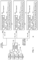
- FIG. 1 is a functional block diagram of an embodiment of a powerline communication control system for LED lighting fixtures.
- FIG. 2 is a functional block diagram of an embodiment of a master controller of a powerline communication control system for LED lighting fixtures.
- FIG. 3 is a functional block diagram of an embodiment of a slave LED lighting fixture unit of a powerline communication control system for LED lighting fixtures.
- FIG. 4 is a functional block diagram of an alternative embodiment of a powerline communication control system for LED lighting fixtures.
- FIG. 5 is a functional block diagram of another embodiment of a powerline communication control system for controlling lighting fixtures.
- FIG. 6 is a flow diagram of an embodiment of a process for controlling lighting fixtures.
- FIG. 7 is a functional block diagram of the OSI Communication Mode.
- FIG. 8 is a flow diagram of the schematic functional diagram of LTK-1 on a microcontroller.
- FIG. 9 is a flow diagram of individual functional blocks of LTK on microcontroller internal structure, and is analogous to FIGS. 1 - 3 .
- Powerline communication as referred to herein can be the powerline communication described in detail in U.S. Pat. No. 8,410,630, entitled, “Powerline Communication Control of Light Emitting Diode (LED) Lighting Fixtures,” by Campbell, the entire content of which is incorporated herein by reference.
- Modulation of a frequency shift keying (FSK) carrier used in connection with the technology described herein can be as described in detail in U.S. Pat. No. 5,852,636, entitled, “Method of and Apparatus for Modulation of FSK Carrier in a Very Narrow Band,” by Mathieu, et al., the entire content of which is incorporated herein by reference.
- FSK frequency shift keying
- FIG. 1 includes a schematic block diagram of a powerline communication control system 10 for LED lighting fixtures.
- powerline communication control system 10 includes a conventional power distribution system 12 , such as a 120 volt AC network, at least one master controller 14 and one or more LED fixture slave units 16 , three of which are diagrammatically shown in FIG. 1 . It is to be appreciated that the number of slave units 16 can vary depending upon the particular application.
- the control output 14 A from each master controller 14 is connected via the power distribution system 12 , to supply a separate control input to one or more of the slave units 16 .
- master controller 14 is coupled to one or more conventional dimmer controllers 18 , four of which are diagrammatically shown in FIG. 1 . It is to be appreciated that the number of dimmer controllers 18 can vary depending upon the particular application. Each master controller 14 receives one or more dimmer control inputs 18 A from one or more of the conventional dimmer controllers 18 . It is to be appreciated that the dimmer controller 18 may include, for example, a DMX/RDM controller, a 0-10V Dimmer(s), a TRIAC dimmer(s) or an Electronic Low Voltage (ELV) Dimmer(s) and the dimmer control inputs 18 A are conventional, standard output control signals of the corresponding types of dimmer controllers 18 .
- any conventional electrical controller can be accommodated by providing a suitable interface for obtaining a controller setting.
- Other controllers include current loop controllers as commonly used in the industrial process control of instruments.
- One such class of controllers is known as 4-20 mA controllers.
- the technology of the disclosure is applicable to Ethernet-based protocols, such as Art-Net, streaming architecture for control networks (SACN), or other such protocol.
- SACN streaming architecture for control networks
- the master controller 14 upon receipt of the dimmer control inputs 18 A, first converts the conventional, standard control input or inputs 18 A from the one or more dimmer controllers 18 into corresponding powerline control signals 14 A. Next, the master controller 14 imposes the powerline control signals 14 A onto the wiring of the power distribution system 12 , together with the conventional power signal 12 P present on power distribution system 12 , and also transmits the powerline control signals 14 A through the power distribution system 12 to each one of the slave units 16 .
- the powerline control signals 14 A may be, for example, in the form of a frequency shift keyed (FSK) signal or a differential phase shift keyed (DPSK) signal.
- the command code format of the powerline control signals 14 A may, for example, be that of a commercially available controller format or a version thereof modified for the specific needs of a powerline communication control system 10 or may be designed specific for the powerline communication control system 10 .
- the powerline control signal 14 A may be in the form of broadcast commands to all of the slave units 16 connected with the power distribution system 12 , so that all slave units 16 are controlled concurrently and in parallel with one another. Alternately, the powerline control signals 14 A may be specifically addressed to an individual slave unit 16 , or to groups/subsets of the slave units 16 , thereby allowing individualized control of one or more of the slave units 16 of the powerline communication control system 10 .
- slave unit 16 includes one or more LED lighting units 16 L. It is noted that only three slave units 16 are diagrammatically shown in FIG. 1 , but it is to be appreciated that the quantity of LED lighting units 16 L can vary depending upon the particular application.
- Each slave unit 16 also includes a communication and power supply node 16 A. As indicated, each communication and power supply node 16 A has a power and control input 16 B, 16 B which is connected with the power distribution system 12 in order to receive both the powerline control signals 14 A and the power signal 12 P from the power distribution system 12 . As indicated in FIG.
- the communication and power supply node 16 A of each slave unit 16 initially separates the received powerline control signals 14 A from the received power signal 12 P, and then generates a DC power output 16 P from the power signal 12 P, and then supplies the generated DC power signal 16 P to the lighting units 16 L in order to power the lighting units 16 L as controlled by the master controller 14 .
- the communication and power supply node 16 A of each slave unit 16 also decodes the received powerline control signals 14 A and, in turn, then generates corresponding lighting control commands 16 C and subsequently supplies the control commands 16 C to the lighting units 16 L so as to control the operation of the lighting units 16 L.
- FIGS. 2 and 3 include detailed schematic block diagrams of master controller 14 and the slave unit 16 , respectively, according to some exemplary embodiments.
- each master controller 14 includes one or more dimmer control conversion circuits 14 B for converting the control inputs 18 A, from the corresponding dimmer controllers 18 , into the corresponding dimmer command inputs 14 C to a microcontroller 14 D which, under control of at least one program(s) residing in a resident memory (not shown for purposes of clarity) to generate the corresponding powerline control signals 14 A, which are then superimposed onto the wires of the power distribution system 12 and the power signal 12 P present thereon by a powerline interface 14 E for transmission of the slave units 16 .
- each master controller 14 also includes other necessary circuitry, such as a power supply 14 F for receiving electrical power from the power distribution system 12 .
- the power and control input 16 B of each communication and power supply node 16 A of each slave unit 16 includes a control input 16 BA, connected to the power distribution system 12 and to the input of a communication interface 16 B which receives the powerline control signals 14 A and the power signal 12 P from the power distribution system 12 , separates the powerline control signals 14 A from the power signal 12 P, and provides corresponding control signals 14 A to an input of a slave control microcontroller 16 D.
- the slave control microcontroller 16 D operating under control of at least one program(s) residing in a memory (not shown for purposes of clarity), in turn, decodes control signals 14 A and generates corresponding slave control signals 16 E, which are converted into corresponding analog or digital lighting control commands 16 C, by a fixture interface 16 F, and then communicated to each one of the lighting units 16 L.
- a power input 16 BP is likewise connected to the power distribution system 12 to receive the power signal 12 with the superimposed powerline control signals 14 A and is connected to the input of a power supply 16 G which, in turn, generates DC power outputs 16 P which are supplied to the circuits of the communication and power supply node 16 A and eventually to the lighting units 16 L of the slave unit 16 .
- FIG. 4 includes a schematic block diagram of an alternate powerline communication control system 10 , according to some exemplary embodiments.
- the illustrated embodiment is generally similar to the embodiments of a powerline communication control system 10 as illustrated in FIGS. 1 , 2 and 3 .
- the dimmer controllers 18 and the dimmer control inputs 18 A are replaced with a human interface controller 20 for generating human interface control inputs 20 A.
- the control inputs 20 A may be generated under the control of, for example, a knob, a slider, a keypad or some other conventional direct human input control device, thereby allowing direct human control of the slave units 16 without the associated intervention and cost of standardized, conventional dimmer controls 18 .
- FIG. 5 includes a functional block diagram of another alternate powerline communication control system 100 for controlling lighting fixtures, according to some exemplary embodiments.
- the system 100 includes a master controller, or adapter 102 , configured to interpret a response or input 103 received from a conventional controller 102 (also referred to as a legacy controller).
- a conventional controller 102 also referred to as a legacy controller.
- the adapter 102 includes a configurable interface 104 suitable for interconnecting to at least one of a variety of different conventional dimmer controllers.
- the adapter 102 also includes a lighting control processor 106 in communication with the configurable interface 104 .
- the lighting control processor 106 is adapted to generate a lighting unit command output in a lighting unit system command format in response to an input received from the conventional controller 102 .
- an input received from the controller 102 provides an indication of a user-adjusted setting of the controller 102 .
- the adapter 102 also includes a power distribution system interface 108 .
- the power distribution system interface 108 is in communication with the lighting control processor 106 and adapted for interconnection to a power distribution system 110 .
- the power distribution system interface 108 is adapted to superimpose the lighting unit system command output of the lighting control processor 106 , onto the power distribution system 110 , to all for dissemination of the lighting unit system command to one or more electrical units to be controlled.
- the adapter 102 can be accommodated within a housing 112 , such as an electrical housing or box 112 adapted to accommodate a typical single or multi-gang electrical switch. Accordingly, in at least some embodiments, such an adapter 102 can be installed together with a conventional controller 102 , within a common multi-gang standard electrical box 112 .
- the box 112 can be fed by an AC power feed or circuit 114 , which can be split within the box 112 (e.g., using wire connectors 116 ) to power the adapter 102 and to a second set of electrical conductors 110 providing AC facility power to the adjustable power to one or more controlled electrical devices.
- the power distribution system interface 108 can be configured to convey an indication of the control setting to the one or more controlled electrical devices (e.g., lighting unit(s)) by any suitable powerline communications (PLC) protocol, such as those described herein and their equivalents.
- PLC powerline communications
- the configurable interface 104 reads an output of the conventional controller 102 .
- the configurable interface 104 provides a stimulus 105 (shown in phantom) that produces a response 103 of the conventional controller 102 , suitable for determining a user-adjusted setting of the controller 102 .
- the configurable interface 104 includes the one or more dimmer control conversion circuits 14 B ( FIG. 2 ).
- the lighting control processor 106 e.g., the microprocessor 14 D of FIG. 2
- each conversion circuit 14 B can be in independently in communication with the microprocessor 14 D through a respective interface.
- the microprocessor 14 D can routinely monitor each of the respective inputs, for example according to a schedule, to detect changes. Upon detecting a change, the microprocessor 14 D can be configured to take a suitable action, such as generating the corresponding powerline control signals 14 A.
- the powerline communication control system 100 also includes at least one device controller 120 .
- the controller can be referred to as a powerline communication node and power supply 102 .
- the device controller 120 includes a power distribution system interface 108 adapted for interconnection to the power distribution system 110 .
- the device controller 120 also referred to as a command receiving interface, is further adapted to separate the lighting unit system command output from the power distribution system 110 when connected thereto.
- the device controller 120 includes a powerline communication modem 122 receiving AC power including any superimposed lighting unit system command outputs.
- the powerline communication modem 122 is adapted to separate the received power and command signals into a separate AC power signal and a separate lighting unit command signal.
- the device controller 120 includes one or more power conversion modules 124 .
- a power conversion module 124 can convert any suitable distributed power, such as AC or DC power, to any other suitable power, such as DC or AC power.
- Such power conversion modules 124 are commonly referred to as one or more of power supplies, power converters, and power inverters.
- the power supply 124 converts 120V AC to a DC power (e.g., 12 volts) suitable for controlling a solid state lighting unit 130 .
- any given power conversion module 124 can be configured to provide more than one output (e.g., +/ ⁇ 12V, 5V, 3.3V). Such power outputs can be used to power one or more of the device controller 120 and any device modules connected thereto.
- the device controller 120 includes a slave control processor 126 in communication with the command receiving interface 122 and adapted to convert the received lighting unit system command output into a corresponding lighting unit control command.
- the lighting unit control command is forwarded to the solid state lighting unit 130 .
- the solid state lighting unit 130 includes a lighting unit interface 132 adapted for interpreting the lighting unit control command and suitably driving the solid state lighting unit 130 in response to the user-adjusted setting of the interconnected one of the conventional dimmers 102 .
- the solid state lighting unit 130 includes one or more LED modules or circuit boards 134 .
- Each circuit board 134 can be populated with one or more lighting elements, or lamps, such as LEDs.
- One or more of the circuit board 134 and the individual LEDs, singly or in groups, can be independently addressable.
- the lighting unit system command outputs can include messages having an address portion and a command portion.
- the slave control processor 126 interprets any received lighting unit system command output, for example, identifying an addressee as well as the command itself.
- the slave control processor 126 converts the received lighting unit system command output into a corresponding lighting unit control command.
- the command can include the address, which can be interpreted to one or more interconnected lighting units 130 .
- the slave control processor 126 can be preconfigured with the addresses of any interconnected lighting units 130 , selectively forwarding such messages to addressed lighting units 130 .
- a lighting unit system command output includes an address of the lighting unit 130 and a command to set the lighting unit 130 at an illumination level corresponding to a user-adjusted setting of the controller 102 .
- the slave control processor 126 provides a suitable lighting unit control command instructing the lighting unit to illuminate at the user-desired setting.
- the lighting unit interface 132 receives the command and drives the LED board(s) 134 with a corresponding current to produce the user-desired illumination.
- the lighting unit 130 can remain at the desired setting until a subsequent command or instruction is received to change the illumination setting, in which instance, the lighting unit 130 will respond accordingly.
- addresses are possible, it can also be possible to provide commands without an address or with a global address, in which instance all interconnected lighting units 130 respond to the instruction. It is also possible for more than one device controller 120 to independently control the same lighting unit 130 .
- the device controller 120 can receive inputs from more than one power distribution circuit 110 , or a single power distribution circuit can be interconnected to more than one device controller 120 .
- the device controller 120 can simply monitor received commands without regard to their source.
- two separate controllers on a three-way controlled lighting unit 130 can independently control a setting of the lighting unit, for example, according to the last command received.
- the device controller 120 is configured to send commands in response to a detected change in a user-adjusted setting of an interconnected controller 102 .
- the device controller 120 can be included within the lighting unit 130 .
- one or more of the power conversion module 124 and the slave control processor 126 can be included in the device controller 120 , as illustrated, in the lighting unit 130 , split between the device controller 120 and lighting unit 130 , or even as separate modules.
- FIG. 6 includes a logical flow diagram of an embodiment of a process 200 for controlling lighting fixtures.
- the process 200 includes determining a user-adjusted setting of a conventional dimmer controller at 205 .
- a lighting unit command output is generated at 210 , responsive to the determined user-adjusted setting.
- the lighting unit command output is distributed at 215 , through power distribution system to at least one lighting fixture.
- the lighting unit command output is converted at 220 , into corresponding lighting unit control command at lighting fixture.
- the lighting unit is controlled at 225 , in response to user-adjusted setting.
- FIGS. 1 and 2 generally show use of a hard wire connection for coupling the standardized, conventional dimmer control 18 to the dimmer control conversion circuit 14 B of the master controller 14 for supplying an input thereto, it is to be appreciated that such input signals can be supplied from the dimmer control 18 to the respective dimmer control conversion circuit 14 B via either a conventional wireless connection or via a conventional Ethernet connection. As such arrangements are conventional and well known in the art, a further detailed description concerning the same is not provided.
- a powerline communication system is manufactured and sold by Lumenpulse Group Inc. of Montreal, Canada, under the trademark LUMENTALK®, which is a registered trademark of Lumenpulse Group Inc.
- the technology is a LUMENTALK® powerline line modem embedded into a microcontroller.
- the LTK-1 ASIC application-specific integrated circuit
- MCU microcontroller
- the LTK-1 ASIC is used as an external “peripheral” to the microcontroller.
- FIG. 8 includes a detailed schematic functional diagram of the technology of the current disclosure, according to some exemplary embodiments.
- FIG. 9 includes a schematic functional block diagram of the technology of the current disclosure, according to some exemplary embodiments.
- FIG. 9 illustrates individual functional blocks of the powerline modem technology of the disclosure, and is analogous to the functional block diagrams of FIGS. 1 - 3 described in detail above. Referring to FIGS. 8 and 9 , the following provides detailed description of the functional blocks for TX (transmit) and RX (receive), which are illustrated in the functional block diagrams of FIGS. 8 and 9 .
- FIG. 9 the diagram illustrates the elements of the present technology and their interaction with powerline communication analog interface 500 , analogous with the powerline communication analog interfaces 14 E and 16 E of FIGS. 2 and 3 , respectively.
- powerline modem 600 illustrated in FIG. 9 is analogous to powerline communication modem 122 of FIG. 5 .
- microcontroller 700 is analogous to microcontrollers 14 D, 16 D and 126 of FIGS. 2 , 3 and 5 , respectively.
- powerline modem 600 of FIG. 9 is illustrated as being implemented within microcontroller 700 .
- microcontroller 126 is implemented separately from powerline communication modem 122 .
- LUMENTALK® communication uses minimal-FSK modulations in the Cenelec D band.
- some FSK modulation (TX) and demodulation (RX) capabilities are implemented.
- TX FSK modulation
- RX demodulation
- TX modulations
- a DAC is used to generate the FSK signal. That DAC is fed with a sine wave table by DMA.
- DMA double buffer
- the MCU While the DAC sends a bit (which takes 220.5 uS), the MCU decides which bit (from the DMA sine wave table) to send next and queues it into the other buffer. When transmitting, this decision happens every 220.5 microseconds. It is noted that without double-buffer DMA, it would be impossible to have a continuous signal coming out of the DAC.
- the txFSM_isr function is triggered at every DMA complete interrupt (220.5 uS).
- the DAC output can be run at, for example, 2 MHz and there are, for example, 441 samples stored in RAM for one bit.
- One bit contains 32 cycles or 31.5 cycles of either F0 or F1 sine waves. This way, each sine wave has around 13 samples per cycle ensuring that the sine wave is “clean” and does not contain too much harmonic on the output.
- the DAC output is then fed to the TX analog front end (AFE).
- AFE TX analog front end
- Each F0 and F1 sine wave tables are stored twice, one starting at 0 degree and the other starting at 180 degrees. This creates a total of 4 sine wave tables to choose from because a bit 0 is only 31.5 cycle of F0.
- every byte to send is cut in half (cut into nibbles) and then encapsulated in a hamming encoded series of bits.
- For each bit of the nibble, there is one parity bit and there is one more parity bit for the whole nibble ((4 data bits+1 control bit)+5 parity bit+1 global parity 11 bits).
- the DAC block refers to the digital to analog converter inside the microcontroller.
- the DAC has 12-bit input capabilities. Its input data is feed by the DMA and runs at a 2 MHz rate using events triggered by the timer 6 (TIM6).
- TIM6 refers to timer number 6 inside the MCU.
- the Timer6 is used to trigger the DAC conversion. In some exemplary embodiments, it triggers at a 2 MHz rate.
- DMA1 stream5 refers to the stream 5 of DMA1 inside the MCU.
- the DMA on this MCU has double buffer capabilities, meaning, it is contemplated that by nature of its design, when the DMA is streaming from one memory location on a buffer, the other buffer can be pointed to another place in memory.
- the present disclosure when the MCU boots, the present disclosure generates in RAM four different digital signals: Frequency 1 (F1), Frequency 1 shifted by 180-degrees (F1-180), frequency 0 (F0) and frequency 0 shifted by 180 degrees (F0-180).
- F1 Frequency 1
- F0 Frequency 1 shifted by 180-degrees
- F0 frequency 0
- F0-180 frequency 0 shifted by 180 degrees
- the DMA transfer complete interrupt service routine jobs (txFSM_isr( )) will be to point the unused buffer to the next frequency needed to form the message. It is worth noting that the DMA1 buffer transmit complete interrupt is executed every time a buffer is empty (every 220.5 microseconds), triggering the txFSM_isr( ).
- startTX( ) is executed every time the present disclosure needs to start a transmission. After “launching” the transmission, startTX( ) will no longer be needed because the txFSM_isr( ) will take care of pointing the DMA to the next digital frequency signal (either F1, F1-180, F0, F0-180) to continue the message.
- startTX( ) stops the reception (disable timer capture (TIM5) interrupt and disables TIM6 (which was in “DATA clock mode” for RX. After that, it starts the output power amplifier. It is contemplated that the output power amplifier needs to be OFF when in receiving mode and ON in transmit mode.
- the two DMA1 buffers are loaded with the right digital waveform frequency addresses. It is envisioned that the DMA1 and DAC are activated and TIM6 is then configured to the transmission rate of 2 MHz and started (TIM6 is now in DAC trigger event mode). The transmission will then be continued by the txFSM_isr( ) after the first DMA1 buffer gets emptied and trigs the transfer complete interrupt.
- startRX( ) is the opposite of startTX( ). It is contemplated that startRX( ) will shut down the power output amplifier, and enable back the interrupt for TIM5 (timer capture) and sets the TIM6 to the data rate (TIM6 is back in “DATA clock mode”).
- txFSM_isr is called from the DMA1 transfer complete interrupt, but it can also be called from the TIM6 update interrupt when the preamble is still ongoing.
- txFSM_isr( ) role is to manage the transmission of a complete message. The first thing it must do to transmit is gain access to the line using the line access mechanism.
- This line access mechanism includes the preamble, which is a series of BURST and LISTEN sections.
- the preamble has nine sections of 10 bits time each (2.205 ms). Each section consists either of transmitting a BURST or listening to the line to see if we “hear” a BURST.
- the present disclosure alternates between BURST and LISTEN section in a random manner.
- the instant disclosure After those nine sections have gone through without hearing a BURST, it is contemplated by the instant disclosure that this indicates access to the line and the ability to transmit the message. If a BURST was heard, the instant disclosure contemplates then waiting for about 20 ms before starting back the preamble again. During this 20 ms, it is contemplated that one can listen to see if the other device trying to get access to the line will take it.
- the present disclosure uses the startRX( ) and startTX( ) function to switch between the LISTENING mode and BURST mode of the preamble.
- txFSM_isr( ) when the BURST ends, the txFSM_isr( ) is triggered from the DMA1 transfer complete interrupt and when the LISTENING mode ends, txFSM_isr( ) is triggered by the TIM6 update interrupt.
- a SYNC message is sent.
- the SYNC has a duration of 11 bit and its purpose is to sync the sender and the receiver data clock (TIM6). It alternates between F0 and F1 for 11 bits.
- the SOP (“Start of Packet” which has 22 bit) is sent.
- the priority (1 byte) and the LumenTalk channel (1 byte) of the message are sent.
- the actual payload is sent nibble by nibble.
- each byte of the message is separated into two nibbles.
- Each nibble is encoded with the hamming encoding provided by the instant disclosure.
- each nibble is transformed from 4 bits to 11 bits with the hamming encoding.
- Each one of those 11 bits correspond to a frequency needed by the present disclosure to output on the DAC.
- either sending the normal version or the one that is phase shifted by 180 degrees is required by the instant disclosure.
- txPLC( ) is a high level function that triggers the transmission state machine in the modem. It was already part of the original design when the LTK1 chip modem was used instead of the LTK on MCU modem.
- the “Input Capture Timer” (ICT) internal peripheral is used (TIM5).
- This internal peripheral of the MCU can measure time (in clock tick) between signal edges. Before entering the signal into the MCU, it is contemplated that it is conditioned by the RX AFE.
- the RX AFE transforms the sine wave from the FSK signal to a square wave with the use of a comparator. This square wave is fed to the MCU ICT.
- the ICT interrupt is called every two edges (two complete cycles) of the incoming signal. This interrupt triggers the realtimeReception function.
- the realtimeReception does the following for each double cycle of the signal: calculate current period(frequency); clip period value if out of range; pass period values through State variable filter; determine if the output of the state variable filter (calculated period) correspond to bit 0 or bit 1 and push them in a shift register; and, detect transitions from bit 0 to bit 1 and from bit 1 to 0. It is envisioned that detected transition are used to sync clock between sender and receiver.
- transitions from one “bit state” (or frequency) to the other in the realtimeReception function are used to sync the clock between sender and the receiver. Since the present disclosure does not contemplate having the clock on a separate wire like some other protocols (SPI or I2C), an approach is implemented to synchronize the sender and the receiver.
- the syncing of the sender and receiver is analogous to syncing (beat matching) two songs on turntables. To “beat match” two songs, it is envisioned that the user will push on one vinyl (in our case the receiving side) to try to sync with the other one.
- the present disclosure contemplates that if the reception clock was not activated (first frequency transition detected), then one can activate the RX clock. Notably, if the RX clock is activated but code is not currently in a receiving state (the “start of packet” (SOP) has not been detected yet), the instant disclosure contemplates looking at where the transition has happen compared to RX clock cycle.
- SOP start of packet
- the realtimeReception function is important to the demodulation of the FSK signal, and is triggered by the interrupt function of the ICT (TIM5).
- the interrupt function of the ICT TIM5
- the MCU With an incoming LumenTalk signal (or just noise on the line), it is contemplated that the MCU is in this interrupt function about 30% to 40% of the time (30% to 40% CPU usage). As implied by its name, this function is envisioned to run in “real-time” as soon as the interrupts initiates, and has the highest priority.
- each bit gets put in a shifting register inside the bitReceived function. It is contemplated that because the bitReceived function resides inside the RTOS, it is executed asynchronously from the real-time section of the code.
- SOP start of packet
- the bitReceived function changes its state to receiving, and starts to decode incoming hamming encoded nibble.
- the function grabs every 11 bits and decode them to data nibble.
- EOP End of Packet
- it grabs the next 4 nibbles and stores them as the cyclic redundancy check (CRC) validation data. It is contemplated that it then validates that the received CRC data correspond to the calculated one.
- CRC cyclic redundancy check
- TIM5 represents the Timer5 in the MCU.
- Timer5 will trigger a timer capture interrupt every two rising edges it has received on its dedicated MCU pin.
- the conditioned signal from RX AFE is a square wave that has the same frequency as the sinewave that was sent on the powerline. So, for every two rising edges of the RX signal, it is envisioned that Timer5 captures the count of its timer and stores it in a register.
- Timer5 runs at the maximum frequency of the MCU, which in some particular exemplary embodiments is 100 MHz, meaning every count of the Timer5 corresponds to 10 nanoseconds.
- ISR interrupt service routine
- the period is then passed to a state variable filter (SVF).
- the low pass of this filter smooths out the periods. It is contemplated that the output of the low pass is then compared with the middle point between the two frequencies. For instance, a frequency for a “1” will have a period value of 1400 and a frequency for a “0” will have a period value of 1378. Anything coming out of the low-pass filter of the SVF that is greater than 1389 will be considered a “1” and everything under 1389 will be considered a “0”. (1400 timer count for two edges corresponds to a “real” signal period of 700 timer counts which is 7000 ns. This corresponds to a frequency of 142857 Hertz.) However, it is contemplated that these parameter values are exemplary only and do not limit the scope of the technology or its applications.
- this “bit reference” corresponding to the period just received is stored in a shift register. Period validity is also stored in another shift register. The “bit reference” shift register is then examined to determine whether a transition in the signal can be identified (0000 followed by 1111 or vice versa). If a transition is spotted, it will behave differently depending on the state of the reception state machine.
- the approach is to synchronize the “data clock” (TIM6) with the transition in the incoming signal to capture the bit at the right time (in the middle of the bit).
- a bit time is 32 cycles of frequency 0 (F0) which in some exemplary embodiments is 220.5 microseconds. It is contemplated that during a bit time, the TIM5 block (timer capture) should trigger the capture interrupt 16 times.
- the present disclosure contemplates pushing or pulling the value of the TIM6 timer by a small amount (fine) to try to be at around half the bit time when the transition is detected. If this aspect of the present disclosure is not yet in a receiving state, it is envisioned that it will push or pull TIM6 by a larger value (coarse), as the value may be already close to the right spot to grab the next bit. It is noted that this is how the present disclosure synchronizes the receiving clock with the transmitter clock.
- TIM6 represents the Timer6 in the MCU. It is contemplated that Timer 6 will trigger an update interrupt when it has reached its autoreload value. This autoreload value is set to the data rate (22050 timer count corresponds to 220.5 microseconds) when in RX mode (DATA clock mode).
- grabBit the interrupt service routine of TIM6 when it is in receiving mode. It is envisioned that every time TIM6 autoreloads (every 220.5 ms), grabBit( ) is executed. grabBit( ) will look at the periods that are stored in the “bit reference” shift register that was filled by realTimeReception( ) and look at the last five values of “bit reference” in the shift register (the last five received period). It should be noted that, in accordance with exemplary embodiments, if the majority of the last five period were considered “1” then the bit to grab is “1” otherwise the bit to grab is “0”. grabBit( ) also looks at the shift register that contains the period validity information to determine whether the periods were out of the desired range.
- bitReceived( ) is passed on to an RTOS function called bitReceived( ) using a Queue which is a RTOS mechanism to transmit data between an ISR and a Thread.
- bitReceived is the last part of the RX Modem section, and is slightly higher level and contains more code. It is envisioned that bitReceived will be executed every time grabBit( ) sends a queue containing the last received bit information. Since it is in the “RTOS section” and not the “real time” section, it should be noted that it might not be executed right after grabBit( ). At some point in the execution, it is contemplated that there could be multiple bit in the queue waiting to be serviced by bitReceived( ). First, it is envisioned that the function will extract the info that grabBit( ) has sent.
- the bit that was received is added to the RX shift register. It is contemplated that this RX shift register is then passed to a hamming decoder. The output of that hamming decoder is then compared with the start of packet (SOP) value to see if a start of packet was received. If yes, bitReceived( ) will shift its state machine to the “data reception” mode. In data reception mode, every 11 bits, it is envisioned that the shift register will be passed to the hamming decoder to get the actual nibble (half a byte) that was received.
- SOP start of packet
- nibble by nibble the received signal is reconstructed and stored in a circular buffer until an End of Packet (EOP) is received. Every time a new nibble is received, the CRC is computed. After the EOP is received, it is contemplated that the next 4 nibbles are stored in a different place because they contain the computed CRC from the source. Notably, it is envisioned that the CRC from the source is then compared with the CRC computed internally to see if they match.
- EOP End of Packet
- the received message descriptor (start address in circular buffer, message length) is sent using an RTOS queue to the rxPlc( ) function. It is contemplated that rxPlc was already part of the original design when the LTK-1 chip modem was used instead of the LTK-2.
- the LTK1 chip when sending data over the powerline, uses a media access control (MAC) system to ensure there are no collisions between multiple senders when in broadcast mode.
- MAC media access control
- the chip Before sending a start of packet, the chip will execute the “preamble” section. This section of 90 bits is constructed of nine 10-bit messages. In a random manner, it is envisioned that the chip will either listen or send a burst (0101010101—10 bits which goes from 0 to 1). If it hears a burst when listening, this means another modem wants to talk, and the chip will wait for this modem to start sending before trying again to send its message.
- MAC media access control
- the receive and transmit sides operate in an alternating manner, as it was created after both modules were almost completed.
- the MAC is then just a state machine that switches from the transmit states to the receive states based on a random number. This state machine resides in the txFSM_isr function.
- the bitreceived function will look out for a burst packet pattern in its shift register.
- the modem of the disclosure could be used on other mediums than the powerline. As an illustrative example, it could potentially be used on a dedicated line or on a DC bus. As an additional illustrative example, it could be modified to be used at other frequencies than the Cenelec D band. With modification to the firmware, it is envisioned that a standalone modem that could be used with another MCU (just like the regular LTK-1 ASIC modem) can be created.
Abstract
Description
Claims (21)
Priority Applications (2)
| Application Number | Priority Date | Filing Date | Title |
|---|---|---|---|
| US17/557,238 US11778715B2 (en) | 2020-12-23 | 2021-12-21 | Apparatus and method for powerline communication control of electrical devices |
| CA3143822A CA3143822A1 (en) | 2020-12-23 | 2021-12-23 | Apparatus and method for powerline communication control of electrical devices |
Applications Claiming Priority (2)
| Application Number | Priority Date | Filing Date | Title |
|---|---|---|---|
| US202063129881P | 2020-12-23 | 2020-12-23 | |
| US17/557,238 US11778715B2 (en) | 2020-12-23 | 2021-12-21 | Apparatus and method for powerline communication control of electrical devices |
Publications (2)
| Publication Number | Publication Date |
|---|---|
| US20220201826A1 US20220201826A1 (en) | 2022-06-23 |
| US11778715B2 true US11778715B2 (en) | 2023-10-03 |
Family
ID=82022833
Family Applications (1)
| Application Number | Title | Priority Date | Filing Date |
|---|---|---|---|
| US17/557,238 Active US11778715B2 (en) | 2020-12-23 | 2021-12-21 | Apparatus and method for powerline communication control of electrical devices |
Country Status (2)
| Country | Link |
|---|---|
| US (1) | US11778715B2 (en) |
| CA (1) | CA3143822A1 (en) |
Families Citing this family (1)
| Publication number | Priority date | Publication date | Assignee | Title |
|---|---|---|---|---|
| EP3800792B1 (en) * | 2019-10-02 | 2022-08-03 | Zumtobel Lighting GmbH | Communication adaptor for a light trunking system, light trunking system comprising at least two such communication adaptors, and method for communicating data over such a light trunking system |
Citations (89)
| Publication number | Priority date | Publication date | Assignee | Title |
|---|---|---|---|---|
| US4815106A (en) | 1986-04-16 | 1989-03-21 | Adaptive Networks, Inc. | Power line communication apparatus |
| US4889999A (en) | 1988-09-26 | 1989-12-26 | Lutron Electronics Co., Inc. | Master electrical load control system |
| US5260974A (en) | 1991-05-10 | 1993-11-09 | Echelon Corporation | Adaptive carrier detection |
| US5350977A (en) | 1992-06-15 | 1994-09-27 | Matsushita Electric Works, Ltd. | Luminaire of variable color temperature for obtaining a blend color light of a desired color temperature from different emission-color light sources |
| US5455490A (en) | 1984-08-15 | 1995-10-03 | Callahan; Michael | Power and signal distribution in lighting systems |
| US5668446A (en) | 1995-01-17 | 1997-09-16 | Negawatt Technologies Inc. | Energy management control system for fluorescent lighting |
| US5828293A (en) | 1997-06-10 | 1998-10-27 | Northern Telecom Limited | Data transmission over a power line communications system |
| GB2335334A (en) | 1998-03-13 | 1999-09-15 | And Software Limited | Transmitting data over low voltage power distribution system |
| US20020065583A1 (en) | 2000-11-30 | 2002-05-30 | Matsushita Electric Works, Ltd. | Setting apparatus and setting method each for setting setting information in electric power line carrier communication terminal apparatus |
| US20020163316A1 (en) | 1997-08-26 | 2002-11-07 | Lys Ihor A. | Methods and apparatus for sensor responsive illumination of liquids |
| US20030146715A1 (en) | 2002-02-01 | 2003-08-07 | Suomi Eric W. | Extraction of accessory power from a signal supplied to a luminaire from a phase angle dimmer |
| US6664745B2 (en) | 1999-09-10 | 2003-12-16 | Richard S. Belliveau | Apparatus for digital communications with multiparameter light fixtures |
| EP1460775A1 (en) | 2003-03-18 | 2004-09-22 | Magnetek S.p.A. | Lighting control with power line modem |
| EP1465464A2 (en) | 2003-04-05 | 2004-10-06 | Theben AG | Dimmer booster |
| US20040225811A1 (en) | 2001-04-04 | 2004-11-11 | Fosler Ross M. | Digital addressable lighting interface bridge |
| US6867558B2 (en) | 2003-05-12 | 2005-03-15 | General Electric Company | Method and apparatus for networked lighting system control |
| US20050225976A1 (en) | 2004-04-08 | 2005-10-13 | Integrated Illumination Systems, Inc. | Marine LED lighting network and driver |
| US20060170376A1 (en) | 2005-01-24 | 2006-08-03 | Color Kinetics Incorporated | Methods and apparatus for providing workspace lighting and facilitating workspace customization |
| US20060274540A1 (en) | 2005-06-01 | 2006-12-07 | Johnson Controls Technology Company | Lighting system |
| US20070057641A1 (en) | 2005-09-09 | 2007-03-15 | Control4 Corporation | Device and method for dimming service loads |
| US7230522B2 (en) | 2004-05-06 | 2007-06-12 | Stevens Carlile R | Power line communication device and method |
| US20070233323A1 (en) | 2006-04-04 | 2007-10-04 | Panduit Corp. | Building automation system controller |
| US20070247089A1 (en) | 2004-07-15 | 2007-10-25 | E Light Limited | Lighting system and controller |
| US7307542B1 (en) | 2003-09-03 | 2007-12-11 | Vantage Controls, Inc. | System and method for commissioning addressable lighting systems |
| DE102006028670A1 (en) | 2006-06-22 | 2007-12-27 | Tridonicatco Gmbh & Co. Kg | Dimmable control gear with internal dimming characteristic |
| DE102006062751A1 (en) | 2006-07-21 | 2008-01-31 | Abb Patent Gmbh | Multi-dimmers for use as e.g. master dimmer, have power unit switchable between phase connection and load connection, and processing and control unit with coding unit that adjusts operation of master dimmer or slave dimmer in desired manner |
| DE102007040152A1 (en) | 2006-08-29 | 2008-03-13 | Avago Technologies Ecbu Ip (Singapore) Pte. Ltd. | Light emitting diode lighting equipment for lighting installation and associated lighting method has controlling medium which determines size of output voltage of rectifier circuit |
| US20080150450A1 (en) | 2006-12-21 | 2008-06-26 | Texas Instruments Inc | Systems and methods for led based lighting |
| US20080157939A1 (en) | 2006-12-29 | 2008-07-03 | Sehat Sutardja | Power control device |
| US20080224636A1 (en) | 2007-03-12 | 2008-09-18 | Melanson John L | Power control system for current regulated light sources |
| US7456588B2 (en) | 2006-06-05 | 2008-11-25 | Osram Sylvania Inc. | Arrangement and method for providing power line communication from an AC power source to a circuit for powering a load, and electronic ballasts therefor |
| US20080297065A1 (en) | 2007-06-01 | 2008-12-04 | Honeywell International Inc. | Dual mode searchlight dimming controller systems and methods |
| WO2009013656A1 (en) | 2007-07-06 | 2009-01-29 | Koninklijke Philips Electronics N.V. | Universal dimming method and system |
| JP2009054987A (en) | 2007-08-27 | 2009-03-12 | Topco Innovation Co Ltd | Light-emitting diode light source and light-emitting diode lamp |
| US20090128061A1 (en) | 2007-10-16 | 2009-05-21 | Robert Dilley | Methods and systems for operating and controlling theatrical lighting |
| US20090171510A1 (en) | 2008-01-02 | 2009-07-02 | Intematix Technology Center Corp. | Method and system for controlling led with power line carrier |
| US20090184662A1 (en) | 2008-01-23 | 2009-07-23 | Cree Led Lighting Solutions, Inc. | Dimming signal generation and methods of generating dimming signals |
| AU2009200556A1 (en) | 2008-02-17 | 2009-09-03 | Vukcevic, Rajko Mr | Electric Power Distribution System incorporating current multiplying DC-DC converters |
| WO2009133489A1 (en) | 2008-04-30 | 2009-11-05 | Koninklijke Philips Electronics N.V. | Methods and apparatus for encoding information on an a.c. line voltage |
| US20100090607A1 (en) | 2008-06-12 | 2010-04-15 | 3M Innovative Properties Company | Dimmer and illumination apparatus with amplitude ordered illumination of multiple strings of multiple color light emitting devices |
| US20100102747A1 (en) | 2008-10-28 | 2010-04-29 | General Electric Company | Unified 0-10v and dali dimming interface circuit |
| US20100109558A1 (en) | 2008-11-03 | 2010-05-06 | Tong Fatt Chew | AC to DC LED illumination devices, systems and methods |
| US20100141169A1 (en) | 2007-03-30 | 2010-06-10 | Holdip Limited | Lighting systems |
| US20100176733A1 (en) | 2009-01-14 | 2010-07-15 | Purespectrum, Inc. | Automated Dimming Methods and Systems For Lighting |
| US20100194298A1 (en) | 2008-10-30 | 2010-08-05 | Fuji Electric Systems Co., Ltd. | Led drive device, led drive method and lighting system |
| US7816803B1 (en) | 2007-08-30 | 2010-10-19 | Marvell International Ltd. | Power line control system |
| US20100308739A1 (en) | 2009-06-04 | 2010-12-09 | Exclara Inc. | Apparatus, Method and System for Providing AC Line Power to Lighting Devices |
| US7865252B2 (en) | 2007-01-26 | 2011-01-04 | Autani Corporation | Upgradeable automation devices, systems, architectures, and methods |
| US20110032085A1 (en) | 2009-08-07 | 2011-02-10 | General Electric Company | Apparatus for controlling integrated lighting ballasts in a series scheme |
| US20110043129A1 (en) | 2008-05-07 | 2011-02-24 | Nxp B.V. | Dim range enhancement for led driver conected to phase-cut dimmer |
| US20110050132A1 (en) | 2008-05-07 | 2011-03-03 | Koninklijke Philips Electronics N.V. | Area based lighting control system including local luminaire control |
| US20110050113A1 (en) | 2008-02-15 | 2011-03-03 | Eldolab Holding B.V. | Illumination System Comprising A Light Source And A Control Unit And An Illumination Control System For Controlling A Light Source By Multiple User Interface Surfaces |
| US20110084622A1 (en) | 2009-10-14 | 2011-04-14 | National Semiconductor Corporation | Dimmer decoder with low duty cycle handling for use with led drivers |
| US20110121754A1 (en) | 2006-01-20 | 2011-05-26 | Exclara Inc. | Adaptive Current Regulation for Solid State Lighting |
| US20110140611A1 (en) | 2009-12-10 | 2011-06-16 | General Electric Company | Dimming bridge module |
| WO2011081633A1 (en) | 2009-12-31 | 2011-07-07 | Samir Gandhi | Control system for color lights |
| US20110187275A1 (en) | 2010-02-04 | 2011-08-04 | Ywire Technologies Inc. | Lighting control switch apparatus and system |
| US20110204820A1 (en) | 2008-09-18 | 2011-08-25 | E Craftsmen Corporation | Configurable led driver/dimmer for solid state lighting applications |
| WO2011121011A1 (en) | 2010-04-01 | 2011-10-06 | Tridonic Gmbh & Co Kg | System-voltage transmission branch of an interface of an operating device for light-emitting means |
| US20110276193A1 (en) | 2010-05-04 | 2011-11-10 | Green Ballast Inc. | Energy efficient lighting system |
| US20110291583A1 (en) | 2010-06-01 | 2011-12-01 | Feng-Min Shen | Dimmer circuit applicable for led device and control method thereof |
| WO2012009622A2 (en) | 2010-07-16 | 2012-01-19 | Lumenpulse Lighting Inc. | Powerline communication control of light emitting diode (led) lighting fixtures |
| US20120056556A1 (en) | 2010-09-08 | 2012-03-08 | Osram Sylvania Inc. | Led-based light source having decorative and illumination functions |
| US8164273B1 (en) | 2007-04-27 | 2012-04-24 | Harrington Richard H | Light emitting diode circuits for general lighting |
| US20120098444A1 (en) | 2010-10-21 | 2012-04-26 | Semisilicon Technology Corp. | Driving apparatus for light-emitting diode curtain lamp |
| US20120133298A1 (en) * | 2010-07-16 | 2012-05-31 | Lumenpulse Lighting Inc. | Powerline communication control of light emitting diode (led) lighting fixtures |
| US20120306375A1 (en) | 2011-06-03 | 2012-12-06 | Cree, Inc. | Systems and methods for controlling solid state lighting devices and lighting apparatus incorporating such systems and/or methods |
| US8330380B2 (en) | 2009-04-09 | 2012-12-11 | Semiconductor Components Industries, Llc | Control circuit for light emitting device |
| US8368315B2 (en) | 2007-12-07 | 2013-02-05 | Koninklijke Philips Electronics N.V. | LED lamp color control system and method |
| US8373346B2 (en) | 2007-08-06 | 2013-02-12 | Nxp B.V. | Solid state lighting system and a driver integrated circuit for driving light emitting semiconductor devices |
| US20130049600A1 (en) | 2011-08-25 | 2013-02-28 | Namjin Kim | Lighting device and method of controlling light emitted thereby |
| US20130088171A1 (en) | 2011-10-06 | 2013-04-11 | National Semiconductor Corporation | Led driver having non-linear compensation |
| DE102012006341A1 (en) | 2012-03-28 | 2013-10-02 | Diehl Aerospace Gmbh | LED lighting device with LED lines and method for operating the LED lighting device |
| DE102012006316A1 (en) | 2012-03-28 | 2013-10-02 | Diehl Aerospace Gmbh | LED illumination device for e.g. 230V public electricity main of incandescent lamp in airplane, has short circuit arrangements controlled in super dimming, so that LED subsets are deactivated for partial period of shaft portion |
| US20130278156A1 (en) | 2010-09-30 | 2013-10-24 | Toshiba Lighting & Technology Corporation | Light-emitting diode lighting apparatus, illuminating apparatus and illuminating method |
| US20130278163A1 (en) | 2012-04-23 | 2013-10-24 | Abl Ip Holding Llc | System and method for controlling led segments to provide lighting effects |
| US8569956B2 (en) | 2009-06-04 | 2013-10-29 | Point Somee Limited Liability Company | Apparatus, method and system for providing AC line power to lighting devices |
| US8692786B2 (en) | 2008-06-10 | 2014-04-08 | Koninklijke Philips N.V. | User interface device and method for controlling a connected consumer load, and light system using such user interface device |
| US8698404B2 (en) | 2011-03-24 | 2014-04-15 | Microsemi Corporation | Brightness control for LED lighting |
| US8768493B2 (en) | 2012-04-25 | 2014-07-01 | Lumenpulse Lighting Inc. | Power line light controller system and method |
| US20140320031A1 (en) | 2013-04-26 | 2014-10-30 | Unity Opto Technology Co., Ltd. | Variable power dimming control circuit |
| US20140354178A1 (en) | 2012-01-20 | 2014-12-04 | Osram Sylvania Inc. | Lighting driver having multiple dimming interfaces |
| US8912734B2 (en) | 2011-03-24 | 2014-12-16 | Cirrus Logic, Inc. | Color mixing of electronic light sources with correlation between phase-cut dimmer angle and predetermined black body radiation function |
| US8917026B2 (en) | 2011-12-20 | 2014-12-23 | Lumenetix, Inc. | Linear bypass electrical circuit for driving LED strings |
| US8970131B2 (en) | 2013-02-15 | 2015-03-03 | Cree, Inc. | Solid state lighting apparatuses and related methods |
| US9066405B2 (en) | 2012-07-30 | 2015-06-23 | Cree, Inc. | Lighting device with variable color rendering based on ambient light |
| US20150351191A1 (en) | 2014-05-30 | 2015-12-03 | Cree, Inc. | Wall controller controlling cct |
| US20180368737A1 (en) * | 2016-01-08 | 2018-12-27 | Koninklijke Philips N.V. | Personalized fitness tracking |
| US10838478B1 (en) * | 2017-06-22 | 2020-11-17 | Bretford Manufacturing, Inc. | Power system |
-
2021
- 2021-12-21 US US17/557,238 patent/US11778715B2/en active Active
- 2021-12-23 CA CA3143822A patent/CA3143822A1/en active Pending
Patent Citations (103)
| Publication number | Priority date | Publication date | Assignee | Title |
|---|---|---|---|---|
| US5455490A (en) | 1984-08-15 | 1995-10-03 | Callahan; Michael | Power and signal distribution in lighting systems |
| US4815106A (en) | 1986-04-16 | 1989-03-21 | Adaptive Networks, Inc. | Power line communication apparatus |
| US4889999A (en) | 1988-09-26 | 1989-12-26 | Lutron Electronics Co., Inc. | Master electrical load control system |
| US5260974A (en) | 1991-05-10 | 1993-11-09 | Echelon Corporation | Adaptive carrier detection |
| US5350977A (en) | 1992-06-15 | 1994-09-27 | Matsushita Electric Works, Ltd. | Luminaire of variable color temperature for obtaining a blend color light of a desired color temperature from different emission-color light sources |
| US5668446A (en) | 1995-01-17 | 1997-09-16 | Negawatt Technologies Inc. | Energy management control system for fluorescent lighting |
| US5828293A (en) | 1997-06-10 | 1998-10-27 | Northern Telecom Limited | Data transmission over a power line communications system |
| US20020163316A1 (en) | 1997-08-26 | 2002-11-07 | Lys Ihor A. | Methods and apparatus for sensor responsive illumination of liquids |
| GB2335334A (en) | 1998-03-13 | 1999-09-15 | And Software Limited | Transmitting data over low voltage power distribution system |
| US6664745B2 (en) | 1999-09-10 | 2003-12-16 | Richard S. Belliveau | Apparatus for digital communications with multiparameter light fixtures |
| US20020065583A1 (en) | 2000-11-30 | 2002-05-30 | Matsushita Electric Works, Ltd. | Setting apparatus and setting method each for setting setting information in electric power line carrier communication terminal apparatus |
| US20040225811A1 (en) | 2001-04-04 | 2004-11-11 | Fosler Ross M. | Digital addressable lighting interface bridge |
| US20030146715A1 (en) | 2002-02-01 | 2003-08-07 | Suomi Eric W. | Extraction of accessory power from a signal supplied to a luminaire from a phase angle dimmer |
| EP1460775A1 (en) | 2003-03-18 | 2004-09-22 | Magnetek S.p.A. | Lighting control with power line modem |
| EP1465464A2 (en) | 2003-04-05 | 2004-10-06 | Theben AG | Dimmer booster |
| US6867558B2 (en) | 2003-05-12 | 2005-03-15 | General Electric Company | Method and apparatus for networked lighting system control |
| US7307542B1 (en) | 2003-09-03 | 2007-12-11 | Vantage Controls, Inc. | System and method for commissioning addressable lighting systems |
| US20050225976A1 (en) | 2004-04-08 | 2005-10-13 | Integrated Illumination Systems, Inc. | Marine LED lighting network and driver |
| US7230522B2 (en) | 2004-05-06 | 2007-06-12 | Stevens Carlile R | Power line communication device and method |
| US20070247089A1 (en) | 2004-07-15 | 2007-10-25 | E Light Limited | Lighting system and controller |
| US20060170376A1 (en) | 2005-01-24 | 2006-08-03 | Color Kinetics Incorporated | Methods and apparatus for providing workspace lighting and facilitating workspace customization |
| US20060274540A1 (en) | 2005-06-01 | 2006-12-07 | Johnson Controls Technology Company | Lighting system |
| US20070057641A1 (en) | 2005-09-09 | 2007-03-15 | Control4 Corporation | Device and method for dimming service loads |
| US20110121754A1 (en) | 2006-01-20 | 2011-05-26 | Exclara Inc. | Adaptive Current Regulation for Solid State Lighting |
| US20070233323A1 (en) | 2006-04-04 | 2007-10-04 | Panduit Corp. | Building automation system controller |
| US7456588B2 (en) | 2006-06-05 | 2008-11-25 | Osram Sylvania Inc. | Arrangement and method for providing power line communication from an AC power source to a circuit for powering a load, and electronic ballasts therefor |
| DE102006028670A1 (en) | 2006-06-22 | 2007-12-27 | Tridonicatco Gmbh & Co. Kg | Dimmable control gear with internal dimming characteristic |
| US8111010B2 (en) | 2006-06-22 | 2012-02-07 | Tridonicatco Gmbh & Co. Kg | Dimmable operating device having internal dimming characteristic |
| DE102006062751A1 (en) | 2006-07-21 | 2008-01-31 | Abb Patent Gmbh | Multi-dimmers for use as e.g. master dimmer, have power unit switchable between phase connection and load connection, and processing and control unit with coding unit that adjusts operation of master dimmer or slave dimmer in desired manner |
| DE102007040152A1 (en) | 2006-08-29 | 2008-03-13 | Avago Technologies Ecbu Ip (Singapore) Pte. Ltd. | Light emitting diode lighting equipment for lighting installation and associated lighting method has controlling medium which determines size of output voltage of rectifier circuit |
| US20080150450A1 (en) | 2006-12-21 | 2008-06-26 | Texas Instruments Inc | Systems and methods for led based lighting |
| US20080157939A1 (en) | 2006-12-29 | 2008-07-03 | Sehat Sutardja | Power control device |
| US7865252B2 (en) | 2007-01-26 | 2011-01-04 | Autani Corporation | Upgradeable automation devices, systems, architectures, and methods |
| US20080224636A1 (en) | 2007-03-12 | 2008-09-18 | Melanson John L | Power control system for current regulated light sources |
| US20100141169A1 (en) | 2007-03-30 | 2010-06-10 | Holdip Limited | Lighting systems |
| US8164273B1 (en) | 2007-04-27 | 2012-04-24 | Harrington Richard H | Light emitting diode circuits for general lighting |
| US20080297065A1 (en) | 2007-06-01 | 2008-12-04 | Honeywell International Inc. | Dual mode searchlight dimming controller systems and methods |
| WO2009013656A1 (en) | 2007-07-06 | 2009-01-29 | Koninklijke Philips Electronics N.V. | Universal dimming method and system |
| US8373346B2 (en) | 2007-08-06 | 2013-02-12 | Nxp B.V. | Solid state lighting system and a driver integrated circuit for driving light emitting semiconductor devices |
| JP2009054987A (en) | 2007-08-27 | 2009-03-12 | Topco Innovation Co Ltd | Light-emitting diode light source and light-emitting diode lamp |
| US7816803B1 (en) | 2007-08-30 | 2010-10-19 | Marvell International Ltd. | Power line control system |
| US20090128061A1 (en) | 2007-10-16 | 2009-05-21 | Robert Dilley | Methods and systems for operating and controlling theatrical lighting |
| US8368315B2 (en) | 2007-12-07 | 2013-02-05 | Koninklijke Philips Electronics N.V. | LED lamp color control system and method |
| US20090171510A1 (en) | 2008-01-02 | 2009-07-02 | Intematix Technology Center Corp. | Method and system for controlling led with power line carrier |
| US8115419B2 (en) | 2008-01-23 | 2012-02-14 | Cree, Inc. | Lighting control device for controlling dimming, lighting device including a control device, and method of controlling lighting |
| US20090184662A1 (en) | 2008-01-23 | 2009-07-23 | Cree Led Lighting Solutions, Inc. | Dimming signal generation and methods of generating dimming signals |
| US20110050113A1 (en) | 2008-02-15 | 2011-03-03 | Eldolab Holding B.V. | Illumination System Comprising A Light Source And A Control Unit And An Illumination Control System For Controlling A Light Source By Multiple User Interface Surfaces |
| AU2009200556A1 (en) | 2008-02-17 | 2009-09-03 | Vukcevic, Rajko Mr | Electric Power Distribution System incorporating current multiplying DC-DC converters |
| US8957595B2 (en) | 2008-04-30 | 2015-02-17 | Koniniklijke Philips N.V. | Methods and apparatus for encoding information on an A.C. line voltage |
| WO2009133489A1 (en) | 2008-04-30 | 2009-11-05 | Koninklijke Philips Electronics N.V. | Methods and apparatus for encoding information on an a.c. line voltage |
| US20110043124A1 (en) | 2008-04-30 | 2011-02-24 | Koninklijke Philips Electronics N.V. | Methods and apparatus for encoding information on an a.c. line voltage |
| US20110043129A1 (en) | 2008-05-07 | 2011-02-24 | Nxp B.V. | Dim range enhancement for led driver conected to phase-cut dimmer |
| US20110050132A1 (en) | 2008-05-07 | 2011-03-03 | Koninklijke Philips Electronics N.V. | Area based lighting control system including local luminaire control |
| US8692786B2 (en) | 2008-06-10 | 2014-04-08 | Koninklijke Philips N.V. | User interface device and method for controlling a connected consumer load, and light system using such user interface device |
| US20100090607A1 (en) | 2008-06-12 | 2010-04-15 | 3M Innovative Properties Company | Dimmer and illumination apparatus with amplitude ordered illumination of multiple strings of multiple color light emitting devices |
| US20110204820A1 (en) | 2008-09-18 | 2011-08-25 | E Craftsmen Corporation | Configurable led driver/dimmer for solid state lighting applications |
| US20100102747A1 (en) | 2008-10-28 | 2010-04-29 | General Electric Company | Unified 0-10v and dali dimming interface circuit |
| US20100194298A1 (en) | 2008-10-30 | 2010-08-05 | Fuji Electric Systems Co., Ltd. | Led drive device, led drive method and lighting system |
| US20100109558A1 (en) | 2008-11-03 | 2010-05-06 | Tong Fatt Chew | AC to DC LED illumination devices, systems and methods |
| US20100176733A1 (en) | 2009-01-14 | 2010-07-15 | Purespectrum, Inc. | Automated Dimming Methods and Systems For Lighting |
| US8330380B2 (en) | 2009-04-09 | 2012-12-11 | Semiconductor Components Industries, Llc | Control circuit for light emitting device |
| US8569956B2 (en) | 2009-06-04 | 2013-10-29 | Point Somee Limited Liability Company | Apparatus, method and system for providing AC line power to lighting devices |
| US20100308739A1 (en) | 2009-06-04 | 2010-12-09 | Exclara Inc. | Apparatus, Method and System for Providing AC Line Power to Lighting Devices |
| US20110032085A1 (en) | 2009-08-07 | 2011-02-10 | General Electric Company | Apparatus for controlling integrated lighting ballasts in a series scheme |
| US8947010B2 (en) | 2009-10-14 | 2015-02-03 | Nationl Semiconductor Corporation | Dimmer decoder with low duty cycle handling for use with LED drivers |
| US20110084622A1 (en) | 2009-10-14 | 2011-04-14 | National Semiconductor Corporation | Dimmer decoder with low duty cycle handling for use with led drivers |
| US20110140611A1 (en) | 2009-12-10 | 2011-06-16 | General Electric Company | Dimming bridge module |
| WO2011081633A1 (en) | 2009-12-31 | 2011-07-07 | Samir Gandhi | Control system for color lights |
| US20110187275A1 (en) | 2010-02-04 | 2011-08-04 | Ywire Technologies Inc. | Lighting control switch apparatus and system |
| WO2011121011A1 (en) | 2010-04-01 | 2011-10-06 | Tridonic Gmbh & Co Kg | System-voltage transmission branch of an interface of an operating device for light-emitting means |
| US20110276193A1 (en) | 2010-05-04 | 2011-11-10 | Green Ballast Inc. | Energy efficient lighting system |
| US20110291583A1 (en) | 2010-06-01 | 2011-12-01 | Feng-Min Shen | Dimmer circuit applicable for led device and control method thereof |
| US8508147B2 (en) | 2010-06-01 | 2013-08-13 | United Power Research Technology Corp. | Dimmer circuit applicable for LED device and control method thereof |
| US9307619B2 (en) | 2010-07-16 | 2016-04-05 | Lumenopulse Lighting Inc. | Powerline communication control of light emitting diode (LED) lighting fixtures |
| US8759999B2 (en) | 2010-07-16 | 2014-06-24 | Lumenpulse Lighting, Inc. | Powerline communication control of light emitting diode (LED) lighting fixtures |
| US20120133298A1 (en) * | 2010-07-16 | 2012-05-31 | Lumenpulse Lighting Inc. | Powerline communication control of light emitting diode (led) lighting fixtures |
| WO2012009622A2 (en) | 2010-07-16 | 2012-01-19 | Lumenpulse Lighting Inc. | Powerline communication control of light emitting diode (led) lighting fixtures |
| US9024464B2 (en) | 2010-07-16 | 2015-05-05 | Lumenpulse Lighting Inc. | Powerline communication control of light emitting diode (LED) lighting fixtures |
| US9622329B2 (en) | 2010-07-16 | 2017-04-11 | Lumenpulse Lighting Inc. | Powerline communication control of light emitting diode (LED) lighting fixtures |
| US8410630B2 (en) | 2010-07-16 | 2013-04-02 | Lumenpulse Lighting Inc. | Powerline communication control of light emitting diode (LED) lighting fixtures |
| US10462879B2 (en) | 2010-07-16 | 2019-10-29 | Lumenpulse Group Inc. | Powerline communication control of light emitting diode (LED) lighting fixtures |
| US20120056556A1 (en) | 2010-09-08 | 2012-03-08 | Osram Sylvania Inc. | Led-based light source having decorative and illumination functions |
| US20130278156A1 (en) | 2010-09-30 | 2013-10-24 | Toshiba Lighting & Technology Corporation | Light-emitting diode lighting apparatus, illuminating apparatus and illuminating method |
| US20120098444A1 (en) | 2010-10-21 | 2012-04-26 | Semisilicon Technology Corp. | Driving apparatus for light-emitting diode curtain lamp |
| US8698404B2 (en) | 2011-03-24 | 2014-04-15 | Microsemi Corporation | Brightness control for LED lighting |
| US8912734B2 (en) | 2011-03-24 | 2014-12-16 | Cirrus Logic, Inc. | Color mixing of electronic light sources with correlation between phase-cut dimmer angle and predetermined black body radiation function |
| US20120306375A1 (en) | 2011-06-03 | 2012-12-06 | Cree, Inc. | Systems and methods for controlling solid state lighting devices and lighting apparatus incorporating such systems and/or methods |
| US8766547B2 (en) | 2011-08-25 | 2014-07-01 | Lg Electronics Inc. | Lighting device and method of controlling light emitted thereby |
| US20130049600A1 (en) | 2011-08-25 | 2013-02-28 | Namjin Kim | Lighting device and method of controlling light emitted thereby |
| US20130088171A1 (en) | 2011-10-06 | 2013-04-11 | National Semiconductor Corporation | Led driver having non-linear compensation |
| US8917026B2 (en) | 2011-12-20 | 2014-12-23 | Lumenetix, Inc. | Linear bypass electrical circuit for driving LED strings |
| US20140354178A1 (en) | 2012-01-20 | 2014-12-04 | Osram Sylvania Inc. | Lighting driver having multiple dimming interfaces |
| DE102012006316A1 (en) | 2012-03-28 | 2013-10-02 | Diehl Aerospace Gmbh | LED illumination device for e.g. 230V public electricity main of incandescent lamp in airplane, has short circuit arrangements controlled in super dimming, so that LED subsets are deactivated for partial period of shaft portion |
| US9185759B2 (en) | 2012-03-28 | 2015-11-10 | Diehl Aerospace | LED lighting device with LED profile and method for operating the LED lighting device |
| DE102012006341A1 (en) | 2012-03-28 | 2013-10-02 | Diehl Aerospace Gmbh | LED lighting device with LED lines and method for operating the LED lighting device |
| US20130278163A1 (en) | 2012-04-23 | 2013-10-24 | Abl Ip Holding Llc | System and method for controlling led segments to provide lighting effects |
| US8768493B2 (en) | 2012-04-25 | 2014-07-01 | Lumenpulse Lighting Inc. | Power line light controller system and method |
| US9066405B2 (en) | 2012-07-30 | 2015-06-23 | Cree, Inc. | Lighting device with variable color rendering based on ambient light |
| US8970131B2 (en) | 2013-02-15 | 2015-03-03 | Cree, Inc. | Solid state lighting apparatuses and related methods |
| US20140320031A1 (en) | 2013-04-26 | 2014-10-30 | Unity Opto Technology Co., Ltd. | Variable power dimming control circuit |
| US20150351191A1 (en) | 2014-05-30 | 2015-12-03 | Cree, Inc. | Wall controller controlling cct |
| US20180368737A1 (en) * | 2016-01-08 | 2018-12-27 | Koninklijke Philips N.V. | Personalized fitness tracking |
| US10838478B1 (en) * | 2017-06-22 | 2020-11-17 | Bretford Manufacturing, Inc. | Power system |
Non-Patent Citations (3)
| Title |
|---|
| International Preliminary Report on Patentability from related PCT Application No. PCT/US2015/021704 dated Oct. 4, 2016. |
| International Search Report dated Jul. 1, 2015 in corresponding PCT Application No. PCT/US2015/021704 (11 pgs.). |
| Machine translation of JP2009054987A, 16 pages. |
Also Published As
| Publication number | Publication date |
|---|---|
| US20220201826A1 (en) | 2022-06-23 |
| CA3143822A1 (en) | 2022-06-23 |
Similar Documents
| Publication | Publication Date | Title |
|---|---|---|
| US10462879B2 (en) | Powerline communication control of light emitting diode (LED) lighting fixtures | |
| US9006995B2 (en) | Controllable retrofit LED lamps and lighting system having an LED lamp | |
| AU2005317202B2 (en) | Mesh network of intelligent devices communicating via powerline and radio frequency | |
| US9320119B2 (en) | System-voltage transmission branch of an interface of an operating device for light-emitting means | |
| CN101218756B (en) | Communications device and communications method | |
| US10165657B2 (en) | Driver circuit for a light source and method of transmitting data over a power line | |
| EP2976825B1 (en) | Dc power distribution system | |
| US11778715B2 (en) | Apparatus and method for powerline communication control of electrical devices | |
| CN102377456A (en) | Method and device for communicating through load conducting wire | |
| CN103763822B (en) | Control information transmitting system and control information sending and receiving method and device | |
| WO2012009622A2 (en) | Powerline communication control of light emitting diode (led) lighting fixtures | |
| CN106714424A (en) | Multi-control output type DALI signal conversion device | |
| US10555404B2 (en) | Systems and methods for dimming light sources | |
| TW201532478A (en) | DALI control system and method | |
| CA2895706C (en) | Powerline communication control of light emitting diode (led) lighting fixtures | |
| US11889607B2 (en) | Lighting control system using pulsed power and single pair ethernet | |
| US20240130026A1 (en) | Load Power Control System Using Fault Managed Power and Single Pair Ethernet | |
| WO2022146621A1 (en) | Lighting control system using pulsed power and single pair ethernet |
Legal Events
| Date | Code | Title | Description |
|---|---|---|---|
| AS | Assignment |
Owner name: LMPG INC., CANADA Free format text: ASSIGNMENT OF ASSIGNORS INTEREST;ASSIGNORS:TOUSIGNANT GENDRON, WILLIAM;LEPAGE, MARIO;CAMPBELL, GREG;AND OTHERS;SIGNING DATES FROM 20211216 TO 20211220;REEL/FRAME:058445/0099 |
|
| FEPP | Fee payment procedure |
Free format text: ENTITY STATUS SET TO UNDISCOUNTED (ORIGINAL EVENT CODE: BIG.); ENTITY STATUS OF PATENT OWNER: LARGE ENTITY |
|
| STPP | Information on status: patent application and granting procedure in general |
Free format text: DOCKETED NEW CASE - READY FOR EXAMINATION |
|
| STPP | Information on status: patent application and granting procedure in general |
Free format text: NOTICE OF ALLOWANCE MAILED -- APPLICATION RECEIVED IN OFFICE OF PUBLICATIONS |
|
| AS | Assignment |
Owner name: ROYNAT CAPITAL INC., CANADA Free format text: SECURITY INTEREST;ASSIGNORS:LMPG INC.;LUMENPULSE LIGHTING CORP.;STERNBERG LANTERNS, INC.;AND OTHERS;REEL/FRAME:064009/0205 Effective date: 20230608 Owner name: NATIONAL BANK OF CANADA, CANADA Free format text: SECURITY INTEREST;ASSIGNOR:LMPG INC.;REEL/FRAME:064009/0080 Effective date: 20230608 |
|
| STPP | Information on status: patent application and granting procedure in general |
Free format text: AWAITING TC RESP., ISSUE FEE NOT PAID |
|
| STPP | Information on status: patent application and granting procedure in general |
Free format text: PUBLICATIONS -- ISSUE FEE PAYMENT RECEIVED |
|
| STPP | Information on status: patent application and granting procedure in general |
Free format text: PUBLICATIONS -- ISSUE FEE PAYMENT VERIFIED |
|
| STCF | Information on status: patent grant |
Free format text: PATENTED CASE |