EP2234187A1 - Organic Light Emitting Display Device - Google Patents
Organic Light Emitting Display Device Download PDFInfo
- Publication number
- EP2234187A1 EP2234187A1 EP10154587A EP10154587A EP2234187A1 EP 2234187 A1 EP2234187 A1 EP 2234187A1 EP 10154587 A EP10154587 A EP 10154587A EP 10154587 A EP10154587 A EP 10154587A EP 2234187 A1 EP2234187 A1 EP 2234187A1
- Authority
- EP
- European Patent Office
- Prior art keywords
- substrate
- light emitting
- dam member
- region
- organic light
- Prior art date
- Legal status (The legal status is an assumption and is not a legal conclusion. Google has not performed a legal analysis and makes no representation as to the accuracy of the status listed.)
- Granted
Links
Images


Classifications
-
- H—ELECTRICITY
- H10—SEMICONDUCTOR DEVICES; ELECTRIC SOLID-STATE DEVICES NOT OTHERWISE PROVIDED FOR
- H10K—ORGANIC ELECTRIC SOLID-STATE DEVICES
- H10K59/00—Integrated devices, or assemblies of multiple devices, comprising at least one organic light-emitting element covered by group H10K50/00
- H10K59/80—Constructional details
- H10K59/87—Passivation; Containers; Encapsulations
- H10K59/871—Self-supporting sealing arrangements
- H10K59/8722—Peripheral sealing arrangements, e.g. adhesives, sealants
-
- H—ELECTRICITY
- H05—ELECTRIC TECHNIQUES NOT OTHERWISE PROVIDED FOR
- H05B—ELECTRIC HEATING; ELECTRIC LIGHT SOURCES NOT OTHERWISE PROVIDED FOR; CIRCUIT ARRANGEMENTS FOR ELECTRIC LIGHT SOURCES, IN GENERAL
- H05B33/00—Electroluminescent light sources
- H05B33/02—Details
- H05B33/04—Sealing arrangements, e.g. against humidity
-
- H—ELECTRICITY
- H10—SEMICONDUCTOR DEVICES; ELECTRIC SOLID-STATE DEVICES NOT OTHERWISE PROVIDED FOR
- H10K—ORGANIC ELECTRIC SOLID-STATE DEVICES
- H10K50/00—Organic light-emitting devices
- H10K50/80—Constructional details
- H10K50/84—Passivation; Containers; Encapsulations
- H10K50/842—Containers
- H10K50/8426—Peripheral sealing arrangements, e.g. adhesives, sealants
-
- H—ELECTRICITY
- H10—SEMICONDUCTOR DEVICES; ELECTRIC SOLID-STATE DEVICES NOT OTHERWISE PROVIDED FOR
- H10K—ORGANIC ELECTRIC SOLID-STATE DEVICES
- H10K50/00—Organic light-emitting devices
- H10K50/80—Constructional details
- H10K50/84—Passivation; Containers; Encapsulations
- H10K50/842—Containers
- H10K50/8428—Vertical spacers, e.g. arranged between the sealing arrangement and the OLED
-
- H—ELECTRICITY
- H10—SEMICONDUCTOR DEVICES; ELECTRIC SOLID-STATE DEVICES NOT OTHERWISE PROVIDED FOR
- H10K—ORGANIC ELECTRIC SOLID-STATE DEVICES
- H10K59/00—Integrated devices, or assemblies of multiple devices, comprising at least one organic light-emitting element covered by group H10K50/00
- H10K59/10—OLED displays
- H10K59/12—Active-matrix OLED [AMOLED] displays
-
- H—ELECTRICITY
- H10—SEMICONDUCTOR DEVICES; ELECTRIC SOLID-STATE DEVICES NOT OTHERWISE PROVIDED FOR
- H10K—ORGANIC ELECTRIC SOLID-STATE DEVICES
- H10K59/00—Integrated devices, or assemblies of multiple devices, comprising at least one organic light-emitting element covered by group H10K50/00
- H10K59/80—Constructional details
- H10K59/87—Passivation; Containers; Encapsulations
- H10K59/871—Self-supporting sealing arrangements
- H10K59/8723—Vertical spacers, e.g. arranged between the sealing arrangement and the OLED
-
- H—ELECTRICITY
- H10—SEMICONDUCTOR DEVICES; ELECTRIC SOLID-STATE DEVICES NOT OTHERWISE PROVIDED FOR
- H10K—ORGANIC ELECTRIC SOLID-STATE DEVICES
- H10K71/00—Manufacture or treatment specially adapted for the organic devices covered by this subclass
-
- H—ELECTRICITY
- H10—SEMICONDUCTOR DEVICES; ELECTRIC SOLID-STATE DEVICES NOT OTHERWISE PROVIDED FOR
- H10K—ORGANIC ELECTRIC SOLID-STATE DEVICES
- H10K71/00—Manufacture or treatment specially adapted for the organic devices covered by this subclass
- H10K71/40—Thermal treatment, e.g. annealing in the presence of a solvent vapour
- H10K71/421—Thermal treatment, e.g. annealing in the presence of a solvent vapour using coherent electromagnetic radiation, e.g. laser annealing
Definitions
- the following description relates to an organic light emitting display device.
- An organic light emitting display device has a relatively high viewing angle, high contrast, high response speed, low power consumption, etc., so that its field of applications has been expanded from a personal portable equipment such as an MP3 player and a cellular phone to a television (TV). In addition, the thickness of the organic light emitting display device has been gradually reduced due to user demand.
- the thickness of the organic light emitting display device is reduced too much, it may cause a difficulty in securing mechanical reliability of the organic light emitting display device if the device is dropped and/or distorted. That is, if the mechanical reliability of the organic light emitting display device is not secured, its sealing can be easily broken even by a small impact so that life span characteristics thereof are deteriorated.
- organic light emitting elements that constitute a pixel include organic material that is relatively weak against attack from moisture and/or oxygen, material of an accompanying sealant has a great influence on the mechanical reliability of the organic light emitting display device and in protecting the organic light emitting elements from moisture and/or oxygen using the sealant.
- An aspect of an embodiment of the present invention is directed toward an organic light emitting display device that can effectively block infiltration of moisture or oxygen and improve mechanical reliability.
- An aspect of an embodiment of the present invention is directed toward an organic light emitting display device that can prevent or protect an inorganic sealant from being contaminated by a sealant.
- An aspect of an embodiment of the present invention is directed toward an organic light emitting display device in which a space between a substrate on which a light emitting device is formed and a sealing substrate is filled with a sealant.
- An embodiment of the present invention provides an organic light emitting display device.
- the organic light emitting display device includes: a first substrate; a plurality of light emitting elements on the first substrate; a second substrate facing the first substrate; a primary dam member between the first substrate and the second substrate and surrounding the plurality of light emitting elements; a filler filled between the first substrate and the second substrate and in a first region defined by the primary dam member; an auxiliary dam member between the first substrate and the second substrate and in a second region outside the first region, the auxiliary dam member being composed of porous material; and an inorganic sealant between the first substrate and the second substrate and in a third region outside the first region and the second region, the inorganic sealant being jointed to the first substrate and the second substrate.
- the primary dam member has a width ranging from 50 ⁇ m to 100mm and/or a height above 10 ⁇ m.
- the auxiliary dam member is formed having a width between 50 ⁇ m and 100 ⁇ m.
- the inorganic sealant has a width ranging from 100 ⁇ m to 200mm and/or a height in the range 1 ⁇ m-100 ⁇ m.
- the distance between the primary dam member and the auxiliary dam member ranges from 10 ⁇ m to 20mm.
- the distance between the auxiliary dam member and the inorganic sealant ranges from 10 ⁇ m to 20mm.
- the organic light emitting display device can effectively block infiltration of moisture and/or oxygen by using the inorganic sealant and/or improve pressure-resistance characteristics, making it possible to have high life span characteristics and mechanical reliability. Also, since the filler overflowing the dam member (or the primary dam member) is absorbed by the porous auxiliary dam member while the substrate on which the light emitting elements are formed is jointed to the sealing substrate, the contamination of the inorganic sealant by the filler is blocked or prevented, making it possible to reduce or minimize the sealing defect.
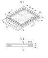
- FIG. 1 is a perspective schematic view of an organic light emitting display device according to an embodiment of the present invention
- FIG. 2 is a cross-sectional schematic view of the organic light emitting display device taken along line I1-I2 of FIG. 1 ;
- FIG. 3 is a cross-sectional schematic view of the organic light emitting elements of FIG. 1 ;
- FIGS. 4A and 4B are plan schematic views showing a method for manufacturing an organic light emitting display device according to an embodiment of the present invention.
- FIGS. 5A, 5B, 5C , 5D, and 5E are cross-sectional schematic views showing a method for manufacturing an organic light emitting display device according to an embodiment of the present invention.
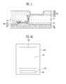
- FIG. 6 is a cross-sectional schematic view of an organic light emitting display device explaining an embodiment of the present invention.
- a use of inorganic sealant that effectively blocks infiltration of moisture and/or oxygen may be considered as being effective in order to improve life span characteristics of an organic light emitting display device.
- the inorganic material is easily released by impact or distortion, thereby deteriorating mechanical reliability.
- An embodiment of the present invention provides an organic light emitting display device having improved life span characteristics by improving the use of the inorganic sealant that effectively blocks infiltration of moisture and/or oxygen.
- FIG. 1 is a perspective schematic view explaining an organic light emitting display device according to an embodiment of the present invention
- FIG. 2 is a cross-sectional schematic view of the organic light emitting display device taken along line 11-12 of FIG. 1 .
- the organic light emitting display device includes: a substrate 100 on which a plurality of light emitting elements 130 are formed; a sealing substrate 200 facing (or opposed to) the substrate 100; a dam member (or primary dam member) 220 provided between the substrate 100 and the sealing substrate 200 and surrounding the plurality of light emitting elements 130; a filler 300 filled between the substrate 100 and the sealing substrate 200 and in a first region defined by the dam member 220 (or defined by an inner side of the dam member 220); an auxiliary dam member 230 provided between the substrate 100 and the sealing substrate 200 and in a second region outside the first region (or defined by an outer side of the dam member 220); and an inorganic sealant 210 provided between the substrate 100 and the sealing substrate 200, in the third region outside of the first and second regions (or defined by an outer side of the auxiliary dam member 230), and jointed to the substrate 100 and the sealing substrate 200.
- the substrate 100 is defined with a display region 120 and a non-display region 140 that is a peripheral region of the display region 120.
- the plurality of light emitting elements 130 are formed in the display region 120, and a driving circuit 160 that drives the plurality of light emitting elements 130 is disposed in the non-display region 140.
- the light emitting element 130 which is an organic light emitting element, includes an anode element 131, a cathode electrode 134, and an organic light emitting layer 133 between the anode electrode 131 and the cathode electrode 134.
- the organic light emitting layer 133 is formed on a light emitting region (a region where the anode electrode 131 is exposed) defined by a pixel definition layer 132.
- the organic light emitting layer 133 may include a hole injection layer, a hole transport layer, an electron transport layer, and an electron injection layer.
- a thin film transistor 110 that controls an operation and a capacitor that maintains a signal can be connected to the light emitting element 130.
- the thin film transistor 110 includes a semiconductor layer 112 that provides source and drain regions and a channel region, a gate electrode 114 that is insulated from the semiconductor layer 112 by a gate insulating layer 113, and source and drain electrodes 116 that are connected to the semiconductor layer 112 on the source and drain regions through a contact hole formed on an insulating layer 115 and the gate insulating layer 113.
- a buffer layer 111 and a planarization insulating layer 117 are provided and shown in FIG. 3 .
- the sealing substrate 200 is disposed to overlap with portions of the display region 120 and the non-display region.
- the sealing substrate 200 may be made of a transparent material such as glass, and in the case of a bottom emission structure, the sealing substrate 200 may be made of an opaque material.
- the inorganic sealant 210 is made of frit that is melted by laser or infrared rays to be jointed to the substrate 100 and the sealing substrate 200, etc. Such an inorganic sealant 210 is provided between the substrate 100 and the sealing substrate 200 in order to surround the light emitting elements 130, thereby preventing or blocking external moisture and/or oxygen from infiltrating the light emitting elements 130.
- the filler 300 is filled in the first region between the substrate 100 and the sealing substrate 200 and defined by the dam member 220.
- the filler 300 is colorless (transparent) liquid-phase material having transmittance of 90% or more in a visible light region such as a glass substrate.
- the filler 300 may use inert liquid, liquid-phase silicon, silicon oils, epoxy-based, acryl-based, photosensitive resin, etc.
- the inert liquid may be selected from the group consisting of perfluorocarbon and fluorinert that have a high stability, i.e., a reacting material that does not react with or is inert to constituents of the light emitting element 130.
- the liquid-phase silicon and the silicon oils exemplarily have no phase-change in a temperature range from -40°C to 100°C and have volume variation within 5%.
- the silicon oils may be, for example, selected from the group consisting of hexamethyldisiloxane, octamethyltrisiloxane, decamethyltetrasiloxane, dodecamethylpentasiloxane, and polydimethylsiloxanes.
- the dam member 220 maintains the shape of the filler 300 by blocking or preventing the flow of the filler 300.
- the dam member 220 may be made of inorganic material and/or organic material.
- the inorganic material may use frit, and the organic material may use epoxy, epoxy acrylate, silicons, etc.
- the organic material is composed of bisphenol-A type epoxy, cycloaliphatics epoxy resin, phenyl silicon resin, and acrylic epoxy resin, etc.
- the auxiliary dam member 230 absorbs the overflowed filler 300 to block or prevent the filler 300 from being contacted with the inorganic sealant 210.
- the auxiliary dam member 230 is made of suitable porous inorganic and/or organic material that effectively absorbs liquid having a low viscosity and does not generate noxious gas.
- the porous inorganic material may use frit, silica gel, etc.
- the porous organic material may use carbon, foaming resin (Styrofoam), etc.
- the auxiliary dam member 230 is exemplarily formed having a width between 50 and 100 ⁇ m in order to reduce or minimize a dead space and to thereby increase or maximize an absorption effect.
- the present invention will be described in more detail through a method for manufacturing an organic light emitting display device according to an embodiment of the present invention.
- FIGS. 4A and 4B are plan schematic views showing a method for manufacturing an organic light emitting display device according to an embodiment of the present invention
- FIGS. 5A to 5E are cross-sectional schematic views showing a method for manufacturing an organic light emitting display device according to an embodiment of the present invention, wherein FIGS. 5A to 5E show a cross-section of parts of the organic light emitting display device taken along line I11-I12 of FIG. 4B .
- the substrate 100 on which the plurality of light emitting elements 130 are formed is initially prepared.
- the substrate 100 is defined with the display region 120 and the non-display region 140 that is the peripheral region of the display region 120.
- the plurality of light emitting elements 130 may be formed on the substrate 100 and in the display region 120, and a driving circuit 160 that drives the light emitting elements 130 may be disposed on the substrate 100 and in the non-display region 140.
- the light emitting element 130 may be a organic light emitting element that includes the anode electrode 131, the organic light emitting layer 133, and the cathode electrode, and may further include the thin film transistor 110 that controls an operation of the organic light emitting element and a capacitor that maintains a signal.
- a manufacturing process of the organic light emitting element may be appreciated by referring to Korean Laid-Open Patent Publication Nos. 2002-0047889 (laid-open publication date: Jun. 22, 2002 ) and 2003-0092873 (laid-open publication date: Dec. 6, 2003 ), the entire content of which is incorporated herein by reference.
- the sealing substrate 200 that seals the light emitting element 130 on the display region 120 is prepared.
- the sealing substrate 200 may have a size that is overlapped with portions of the display region 120 and the non-display region 140.
- the sealing substrate 200 may be larger than the display region 120 and completely covering the display region 120.
- the sealing substrate 200 may use a transparent substrate such as glass in the case of a top emission structure, and may use an opaque substrate in the case of a bottom emission structure.
- the inorganic sealant 210 is formed along an outer region of the sealing substrate 200.
- the inorganic sealant 210 may use frit, wherein it is coated through a dispenser and/or screen printing process.
- Frit generally refers to glass raw material in a powder shape.
- the frit refers to a paste with an infrared ray absorber, an organic binder, and a filler for reducing thermal expansion coefficient, etc. that are included in a main material, such as Si02, etc. If the frit in the paste state is subject to a dry and/or burning process, the organic binder and moisture are removed so that the frit is hardened.
- the laser and/or infrared absorber may include a transition metal compound, exemplarily, a vanadium compound.
- the dam member 220 is formed on the sealing substrate 200 in a region defined by the inorganic sealant 210 (or defined by the inner side of the inorganic sealant 210) in order to surround the display region 120, and the auxiliary dam member 230 is formed on the sealing substrate 200 between the dam member 220 and the inorganic sealant 210 in order to surround the dam member 220.
- the dam member 220 may be made of organic material and/or inorganic material, and the auxiliary dam member 230 may be made of porous inorganic material and/or organic material that can absorb a filler 300.
- the dam member 220 and the auxiliary dam member 230 may be coated through a dispenser and/or a screen printing process.
- the coated amount is determined by considering the distance from the light emitting element 130 positioned at the outer-most portion of the display region 120 to the inorganic sealant 210 and the height of the dam member 220 and the auxiliary dam member 230. If the height of the dam member 220 and the auxiliary dam member 230 is higher than that of the inorganic sealant 210, it is difficult to join the inorganic sealant 210 to the substrate 100. Therefore, it is exemplar that the height of the dam member 220 and the auxiliary dam member 230 is equal to or lower than that of the inorganic sealant 210.
- the dam member 220 and the auxiliary dam member 230 are made of material having low viscosity which easily collapses if they have been temporarily-hardened in the coated state, so that they are structurally hardened, thereby making it possible to reinforce a dam function.
- the temporary-hardening may be achieved by using heat, electron beam and/or ultraviolet rays according to the material characteristics of the material utilized.
- the dam member 220 and the auxiliary dam member 230 are formed after the inorganic sealant 210 is formed, however, the formation order may be changed according to the design and process conditions.
- the liquid-phase filler 300 is provided to the sealing substrate 200 in the first region defined by the dam member 220 (or defined by the inner side of the dam member 220).
- the filler 300 may be provided through an inkjet, a dispenser, a screen printing or a one drop filling (ODF), etc.
- ODF one drop filling
- the filler 300 having viscosity between 10 -2 and 20 Pa ⁇ s may be loaded onto the sealing substrate 200 in the first region defined by the inner side of the dam member 220 using the ODF equipment. In this case, the appropriate amount to volume of the theoretical inner space may be easily controlled.
- the substrate 100 and the sealing substrate 200 are then disposed to be opposed to each other.
- the substrate 100 is mounted on an upper chuck of the junction device
- the sealing substrate 200 is mounted on a lower chuck thereof
- the substrate 100 is jointed to the sealing substrate 200.
- the filler 300 is filled in the first region defined by the inner side of the dam member 220, and the flow of the filler 300 is prevented by the dam member 220 so that the shape of the filler 300 is maintained.
- the substrate 100 and the sealing substrate 200 can be pressurized so that the space between the light emitting elements 130 and the sealing substrate 200 is completely filled with the filler 300.
- laser and/or infrared rays are emitted along the inorganic material 210 in the state where the substrate 100 is joined to the sealing substrate 200.
- the inorganic sealant 210 is melted to be jointed to the substrate 100 and the sealing substrate 200, such that the light emitting elements 130 are thereby sealed.
- laser and/or infrared rays can be emitted only to a desired region using a mask and/or a protective film (not shown), and the filler 300 can be hardened using heat, electron beam and/or ultraviolet rays (UV) in the state where the elements 130 are sealed as described above.
- UV ultraviolet rays
- the filler 300 may contact the inorganic sealant 210 by overflowing the dam member 220 while the substrate 100 is jointed to the sealing substrate 200 as shown in FIG. 5 .
- the inorganic sealant 210 is contaminated by the filler 300 so that when the inorganic sealant 210 is jointed to the substrate 100 by emitting laser and/or infrared rays, the inorganic sealant 210 is not completely jointed to the substrate 100 so that the sealed state is deteriorated.
- the filler 300 overflowing the dam member 220 is absorbed by the porous auxiliary dam member 230, making it possible to effectively block or prevent the inorganic sealant 210 from being contacted with the filler 300.
- An embodiment of the present invention describes the case where the display region 120 is sealed by the inorganic sealant 210, however, the present invention is not limited thereto, and a driving circuit 160 may also be sealed by the inorganic sealant 210. Also, an embodiment of the present invention describes the case where the inorganic sealant 210 and the auxiliary dam member 230 are formed on the sealing substrate 200, having a single structure, however, the present invention is not limited thereto, and they may be formed on the substrate 100 and/or may be formed to have a double structure or a multiple structure (e.g., a double or multiple layers).
- the inorganic sealant 210 may be formed to have a double structure or a multiple structure in order to enhance a sealing effect, or the auxiliary dam member 220 may be formed having a double structure or a multiple structure in order to effectively block or prevent the defect due to the overflow of the filler 300.
Landscapes
- Physics & Mathematics (AREA)
- Optics & Photonics (AREA)
- Engineering & Computer Science (AREA)
- Electromagnetism (AREA)
- Manufacturing & Machinery (AREA)
- Microelectronics & Electronic Packaging (AREA)
- Electroluminescent Light Sources (AREA)
- Devices For Indicating Variable Information By Combining Individual Elements (AREA)
Abstract
Description
- This application claims priority to and the benefit of Korean Patent Application No.
10-2009-0024984, filed on March 24, 2009 - The following description relates to an organic light emitting display device.
- An organic light emitting display device has a relatively high viewing angle, high contrast, high response speed, low power consumption, etc., so that its field of applications has been expanded from a personal portable equipment such as an MP3 player and a cellular phone to a television (TV). In addition, the thickness of the organic light emitting display device has been gradually reduced due to user demand.
- However, if the thickness of the organic light emitting display device is reduced too much, it may cause a difficulty in securing mechanical reliability of the organic light emitting display device if the device is dropped and/or distorted. That is, if the mechanical reliability of the organic light emitting display device is not secured, its sealing can be easily broken even by a small impact so that life span characteristics thereof are deteriorated.
- In particular, since organic light emitting elements that constitute a pixel include organic material that is relatively weak against attack from moisture and/or oxygen, material of an accompanying sealant has a great influence on the mechanical reliability of the organic light emitting display device and in protecting the organic light emitting elements from moisture and/or oxygen using the sealant.
- An aspect of an embodiment of the present invention is directed toward an organic light emitting display device that can effectively block infiltration of moisture or oxygen and improve mechanical reliability.
- An aspect of an embodiment of the present invention is directed toward an organic light emitting display device that can prevent or protect an inorganic sealant from being contaminated by a sealant.
- An aspect of an embodiment of the present invention is directed toward an organic light emitting display device in which a space between a substrate on which a light emitting device is formed and a sealing substrate is filled with a sealant.
- An embodiment of the present invention provides an organic light emitting display device. The organic light emitting display device includes: a first substrate; a plurality of light emitting elements on the first substrate; a second substrate facing the first substrate; a primary dam member between the first substrate and the second substrate and surrounding the plurality of light emitting elements; a filler filled between the first substrate and the second substrate and in a first region defined by the primary dam member; an auxiliary dam member between the first substrate and the second substrate and in a second region outside the first region, the auxiliary dam member being composed of porous material; and an inorganic sealant between the first substrate and the second substrate and in a third region outside the first region and the second region, the inorganic sealant being jointed to the first substrate and the second substrate. Preferably, the primary dam member has a width ranging from 50µm to 100mm and/or a height above 10µm. Preferably, the auxiliary dam member is formed having a width between 50 µm and 100 µm. Preferably, the inorganic sealant has a width ranging from 100µm to 200mm and/or a height in the range 1µm-100 µm. Preferably, the distance between the primary dam member and the auxiliary dam member ranges from 10 µm to 20mm. Preferably, the distance between the auxiliary dam member and the inorganic sealant ranges from 10 µm to 20mm.
- Here, the organic light emitting display device can effectively block infiltration of moisture and/or oxygen by using the inorganic sealant and/or improve pressure-resistance characteristics, making it possible to have high life span characteristics and mechanical reliability. Also, since the filler overflowing the dam member (or the primary dam member) is absorbed by the porous auxiliary dam member while the substrate on which the light emitting elements are formed is jointed to the sealing substrate, the contamination of the inorganic sealant by the filler is blocked or prevented, making it possible to reduce or minimize the sealing defect.
- The accompanying drawings, together with the specification illustrate exemplary embodiments of the present invention, and, together with the description, serve to explain the principles of the present invention.
-
FIG. 1 is a perspective schematic view of an organic light emitting display device according to an embodiment of the present invention; -
FIG. 2 is a cross-sectional schematic view of the organic light emitting display device taken along line I1-I2 ofFIG. 1 ; -
FIG. 3 is a cross-sectional schematic view of the organic light emitting elements ofFIG. 1 ; -
FIGS. 4A and4B are plan schematic views showing a method for manufacturing an organic light emitting display device according to an embodiment of the present invention; -
FIGS. 5A, 5B, 5C ,5D, and 5E are cross-sectional schematic views showing a method for manufacturing an organic light emitting display device according to an embodiment of the present invention; and -
FIG. 6 is a cross-sectional schematic view of an organic light emitting display device explaining an embodiment of the present invention. - In the following detailed description, only certain exemplary embodiments of the present invention have been shown and described, simply by way of illustration.
As those skilled in the art would realize, the described embodiments may be modified in various different ways, all without departing from the scope of the present invention. Accordingly, the drawings and description are to be regarded as illustrative in nature and not restrictive. In addition, when an element is referred to as being "on" another element, it can be directly on the another element or be indirectly on the another element with one or more intervening elements interposed therebetween. Also, when an element is referred to as being "connected to" another element, it can be directly connected to the another element or be indirectly connected to the another element with one or more intervening elements interposed therebetween. Hereinafter, like reference numerals refer to like elements. - Hereinafter, exemplary embodiments according to the present invention will be described with reference to the accompanying drawings.
- A use of inorganic sealant that effectively blocks infiltration of moisture and/or oxygen may be considered as being effective in order to improve life span characteristics of an organic light emitting display device. However, the inorganic material is easily released by impact or distortion, thereby deteriorating mechanical reliability.
- An embodiment of the present invention provides an organic light emitting display device having improved life span characteristics by improving the use of the inorganic sealant that effectively blocks infiltration of moisture and/or oxygen.
-
FIG. 1 is a perspective schematic view explaining an organic light emitting display device according to an embodiment of the present invention, andFIG. 2 is a cross-sectional schematic view of the organic light emitting display device taken along line 11-12 ofFIG. 1 . - Referring to
FIGS. 1 and 2 , the organic light emitting display device includes: asubstrate 100 on which a plurality oflight emitting elements 130 are formed; asealing substrate 200 facing (or opposed to) thesubstrate 100; a dam member (or primary dam member) 220 provided between thesubstrate 100 and thesealing substrate 200 and surrounding the plurality oflight emitting elements 130; afiller 300 filled between thesubstrate 100 and thesealing substrate 200 and in a first region defined by the dam member 220 (or defined by an inner side of the dam member 220); anauxiliary dam member 230 provided between thesubstrate 100 and thesealing substrate 200 and in a second region outside the first region (or defined by an outer side of the dam member 220); and aninorganic sealant 210 provided between thesubstrate 100 and thesealing substrate 200, in the third region outside of the first and second regions (or defined by an outer side of the auxiliary dam member 230), and jointed to thesubstrate 100 and thesealing substrate 200. - The
substrate 100 is defined with adisplay region 120 and anon-display region 140 that is a peripheral region of thedisplay region 120. The plurality oflight emitting elements 130 are formed in thedisplay region 120, and adriving circuit 160 that drives the plurality oflight emitting elements 130 is disposed in thenon-display region 140. - Referring to
FIG. 3 , thelight emitting element 130, which is an organic light emitting element, includes ananode element 131, acathode electrode 134, and an organiclight emitting layer 133 between theanode electrode 131 and thecathode electrode 134. The organiclight emitting layer 133 is formed on a light emitting region (a region where theanode electrode 131 is exposed) defined by apixel definition layer 132. The organiclight emitting layer 133 may include a hole injection layer, a hole transport layer, an electron transport layer, and an electron injection layer. - Also, a
thin film transistor 110 that controls an operation and a capacitor that maintains a signal can be connected to thelight emitting element 130. Thethin film transistor 110 includes asemiconductor layer 112 that provides source and drain regions and a channel region, agate electrode 114 that is insulated from thesemiconductor layer 112 by agate insulating layer 113, and source anddrain electrodes 116 that are connected to thesemiconductor layer 112 on the source and drain regions through a contact hole formed on aninsulating layer 115 and thegate insulating layer 113. In addition, abuffer layer 111 and aplanarization insulating layer 117 are provided and shown inFIG. 3 . - The sealing
substrate 200 is disposed to overlap with portions of thedisplay region 120 and the non-display region. In the case of a top emission structure, thesealing substrate 200 may be made of a transparent material such as glass, and in the case of a bottom emission structure, thesealing substrate 200 may be made of an opaque material. - The
inorganic sealant 210 is made of frit that is melted by laser or infrared rays to be jointed to thesubstrate 100 and thesealing substrate 200, etc. Such aninorganic sealant 210 is provided between thesubstrate 100 and thesealing substrate 200 in order to surround thelight emitting elements 130, thereby preventing or blocking external moisture and/or oxygen from infiltrating thelight emitting elements 130. - The
filler 300 is filled in the first region between thesubstrate 100 and thesealing substrate 200 and defined by thedam member 220. Thefiller 300 is colorless (transparent) liquid-phase material having transmittance of 90% or more in a visible light region such as a glass substrate. Thefiller 300 may use inert liquid, liquid-phase silicon, silicon oils, epoxy-based, acryl-based, photosensitive resin, etc. - The inert liquid may be selected from the group consisting of perfluorocarbon and fluorinert that have a high stability, i.e., a reacting material that does not react with or is inert to constituents of the
light emitting element 130. Also, the liquid-phase silicon and the silicon oils exemplarily have no phase-change in a temperature range from -40°C to 100°C and have volume variation within 5%. The silicon oils may be, for example, selected from the group consisting of hexamethyldisiloxane, octamethyltrisiloxane, decamethyltetrasiloxane, dodecamethylpentasiloxane, and polydimethylsiloxanes. - The
dam member 220 maintains the shape of thefiller 300 by blocking or preventing the flow of thefiller 300. Thedam member 220 may be made of inorganic material and/or organic material. The inorganic material may use frit, and the organic material may use epoxy, epoxy acrylate, silicons, etc. In the embodiment, the organic material is composed of bisphenol-A type epoxy, cycloaliphatics epoxy resin, phenyl silicon resin, and acrylic epoxy resin, etc. - When the
filler 300 overflows thedam member 220, theauxiliary dam member 230 absorbs the overflowedfiller 300 to block or prevent thefiller 300 from being contacted with theinorganic sealant 210. Theauxiliary dam member 230 is made of suitable porous inorganic and/or organic material that effectively absorbs liquid having a low viscosity and does not generate noxious gas. For example, the porous inorganic material may use frit, silica gel, etc., and the porous organic material may use carbon, foaming resin (Styrofoam), etc. Also, theauxiliary dam member 230 is exemplarily formed having a width between 50 and 100 µm in order to reduce or minimize a dead space and to thereby increase or maximize an absorption effect. - The present invention will be described in more detail through a method for manufacturing an organic light emitting display device according to an embodiment of the present invention.
-
FIGS. 4A and4B are plan schematic views showing a method for manufacturing an organic light emitting display device according to an embodiment of the present invention, andFIGS. 5A to 5E are cross-sectional schematic views showing a method for manufacturing an organic light emitting display device according to an embodiment of the present invention, whereinFIGS. 5A to 5E show a cross-section of parts of the organic light emitting display device taken along line I11-I12 ofFIG. 4B . - Referring to
FIG. 4A , thesubstrate 100 on which the plurality oflight emitting elements 130 are formed is initially prepared. Thesubstrate 100 is defined with thedisplay region 120 and thenon-display region 140 that is the peripheral region of thedisplay region 120. The plurality oflight emitting elements 130 may be formed on thesubstrate 100 and in thedisplay region 120, and adriving circuit 160 that drives thelight emitting elements 130 may be disposed on thesubstrate 100 and in thenon-display region 140. - Referring to
FIG. 3 , thelight emitting element 130 may be a organic light emitting element that includes theanode electrode 131, the organiclight emitting layer 133, and the cathode electrode, and may further include thethin film transistor 110 that controls an operation of the organic light emitting element and a capacitor that maintains a signal. A manufacturing process of the organic light emitting element may be appreciated by referring to Korean Laid-Open Patent Publication Nos.2002-0047889 (laid-open publication date: Jun. 22, 2002 2003-0092873 (laid-open publication date: Dec. 6, 2003 - Referring to
FIGS. 4B and 5A , the sealingsubstrate 200 that seals thelight emitting element 130 on thedisplay region 120 is prepared. The sealingsubstrate 200 may have a size that is overlapped with portions of thedisplay region 120 and thenon-display region 140. The sealingsubstrate 200 may be larger than thedisplay region 120 and completely covering thedisplay region 120. The sealingsubstrate 200 may use a transparent substrate such as glass in the case of a top emission structure, and may use an opaque substrate in the case of a bottom emission structure. - An
inorganic sealant 210 is formed along an outer region of the sealingsubstrate 200. Theinorganic sealant 210 may use frit, wherein it is coated through a dispenser and/or screen printing process. Frit generally refers to glass raw material in a powder shape. However, in embodiments of the present invention, the frit refers to a paste with an infrared ray absorber, an organic binder, and a filler for reducing thermal expansion coefficient, etc. that are included in a main material, such as Si02, etc. If the frit in the paste state is subject to a dry and/or burning process, the organic binder and moisture are removed so that the frit is hardened. The laser and/or infrared absorber may include a transition metal compound, exemplarily, a vanadium compound. - Referring to
FIGS. 4B and 5B , thedam member 220 is formed on the sealingsubstrate 200 in a region defined by the inorganic sealant 210 (or defined by the inner side of the inorganic sealant 210) in order to surround thedisplay region 120, and theauxiliary dam member 230 is formed on the sealingsubstrate 200 between thedam member 220 and theinorganic sealant 210 in order to surround thedam member 220. - The
dam member 220 may be made of organic material and/or inorganic material, and theauxiliary dam member 230 may be made of porous inorganic material and/or organic material that can absorb afiller 300. Thedam member 220 and theauxiliary dam member 230 may be coated through a dispenser and/or a screen printing process. Here, the coated amount is determined by considering the distance from thelight emitting element 130 positioned at the outer-most portion of thedisplay region 120 to theinorganic sealant 210 and the height of thedam member 220 and theauxiliary dam member 230. If the height of thedam member 220 and theauxiliary dam member 230 is higher than that of theinorganic sealant 210, it is difficult to join theinorganic sealant 210 to thesubstrate 100. Therefore, it is exemplar that the height of thedam member 220 and theauxiliary dam member 230 is equal to or lower than that of theinorganic sealant 210. - Also, the
dam member 220 and theauxiliary dam member 230 are made of material having low viscosity which easily collapses if they have been temporarily-hardened in the coated state, so that they are structurally hardened, thereby making it possible to reinforce a dam function. The temporary-hardening may be achieved by using heat, electron beam and/or ultraviolet rays according to the material characteristics of the material utilized. - In one embodiment, the
dam member 220 and theauxiliary dam member 230 are formed after theinorganic sealant 210 is formed, however, the formation order may be changed according to the design and process conditions. - Referring to
FIG. 5C , the liquid-phase filler 300 is provided to the sealingsubstrate 200 in the first region defined by the dam member 220 (or defined by the inner side of the dam member 220). Thefiller 300 may be provided through an inkjet, a dispenser, a screen printing or a one drop filling (ODF), etc. For example, thefiller 300 having viscosity between 10-2 and 20 Pa·s may be loaded onto the sealingsubstrate 200 in the first region defined by the inner side of thedam member 220 using the ODF equipment. In this case, the appropriate amount to volume of the theoretical inner space may be easily controlled. - Referring to
FIG. 5D , thesubstrate 100 and the sealingsubstrate 200 are then disposed to be opposed to each other. For example, thesubstrate 100 is mounted on an upper chuck of the junction device, the sealingsubstrate 200 is mounted on a lower chuck thereof, and then thesubstrate 100 is jointed to the sealingsubstrate 200. As thesubstrate 100 is jointed to the sealingsubstrate 200, thefiller 300 is filled in the first region defined by the inner side of thedam member 220, and the flow of thefiller 300 is prevented by thedam member 220 so that the shape of thefiller 300 is maintained. Here, thesubstrate 100 and the sealingsubstrate 200 can be pressurized so that the space between thelight emitting elements 130 and the sealingsubstrate 200 is completely filled with thefiller 300. - Referring to
FIG. 5E , laser and/or infrared rays are emitted along theinorganic material 210 in the state where thesubstrate 100 is joined to the sealingsubstrate 200. As laser and/or infrared rays are absorbed to generate heat, theinorganic sealant 210 is melted to be jointed to thesubstrate 100 and the sealingsubstrate 200, such that thelight emitting elements 130 are thereby sealed. - When emitting laser and/or infrared rays along the
inorganic sealant 210, laser and/or infrared rays can be emitted only to a desired region using a mask and/or a protective film (not shown), and thefiller 300 can be hardened using heat, electron beam and/or ultraviolet rays (UV) in the state where theelements 130 are sealed as described above. - In a structure where the
auxiliary dam member 230 is not provided as shown inFIG. 6 , thefiller 300 may contact theinorganic sealant 210 by overflowing thedam member 220 while thesubstrate 100 is jointed to the sealingsubstrate 200 as shown inFIG. 5 . In this case, theinorganic sealant 210 is contaminated by thefiller 300 so that when theinorganic sealant 210 is jointed to thesubstrate 100 by emitting laser and/or infrared rays, theinorganic sealant 210 is not completely jointed to thesubstrate 100 so that the sealed state is deteriorated. However, in an embodiment of the present invention having a structure where theauxiliary dam member 230 is provided, thefiller 300 overflowing thedam member 220 is absorbed by the porousauxiliary dam member 230, making it possible to effectively block or prevent theinorganic sealant 210 from being contacted with thefiller 300. - An embodiment of the present invention describes the case where the
display region 120 is sealed by theinorganic sealant 210, however, the present invention is not limited thereto, and adriving circuit 160 may also be sealed by theinorganic sealant 210. Also, an embodiment of the present invention describes the case where theinorganic sealant 210 and theauxiliary dam member 230 are formed on the sealingsubstrate 200, having a single structure, however, the present invention is not limited thereto, and they may be formed on thesubstrate 100 and/or may be formed to have a double structure or a multiple structure (e.g., a double or multiple layers). For example, theinorganic sealant 210 may be formed to have a double structure or a multiple structure in order to enhance a sealing effect, or theauxiliary dam member 220 may be formed having a double structure or a multiple structure in order to effectively block or prevent the defect due to the overflow of thefiller 300. - While the present invention has been described in connection with certain exemplary embodiments, it is to be understood that the invention is not limited to the disclosed embodiments, but, on the contrary, is intended to cover various modifications and equivalent arrangements included within the scope of the appended claims, and equivalents thereof.
Claims (13)
- An organic light emitting display device, comprising:a first substrate (100);a second substrate (200) facing the first substrate (100);a plurality of light emitting elements (130) on a surface of the first substrate (100) facing the second substrate(200);a primary dam member (220) between the first substrate (100) and the second substrate (200) and surrounding the plurality of light emitting elements (130);a filler (300) filled between the first substrate (100) and the second substrate (200) in a first region defined by the primary dam member (220);an auxiliary dam member (230) between the first substrate (100) and the second substrate (200) in a second region outside the first region, the auxiliary dam member (2309 being composed of porous material; andan inorganic sealant (210) between the first substrate (100) and the second substrate (200) in a third region outside the first region and the second region, the inorganic sealant (210) being jointed to the first substrate (100) and the second substrate (200).
- The organic light emitting display device as claimed in claim 1, wherein the filler (300) is composed of a material selected from the group consisting of inert liquids, liquid-phase silicon, silicon oils, epoxy-based resins, acryl-based resins, photosensitive resins, and combinations thereof.
- The organic light emitting display device as claimed in one of the preceding claims, wherein the primary dam member (220) is composed of frit.
- The organic light emitting display device as claimed in one of claims 1 and 2, wherein the primary dam member (220) comprises a material selected from the group consisting of epoxies, epoxy acrylates, bisphenol-A type epoxies, cycloaliphatics epoxy resins, phenyl silicon resins, acrylic epoxy resins, and combinations thereof.
- The organic light emitting display device as claimed in one of the preceding claims, wherein the porous material forming the auxiliary dam member (230) comprises a material selected from the group consisting of frits, carbons, silica gels, foaming resins, and combinations thereof.
- The organic light emitting display device as claimed in one of the preceding claims, wherein the auxiliary dam member (230) has a width between about 50 and about 100 µm.
- The organic light emitting display device as claimed in one of the preceding claims, wherein the inorganic sealant (210) is composed of frit.
- The organic light emitting display device as claimed in claim 7, wherein the frit is a laser or infrared ray melted frit.
- The organic light emitting display device as claimed in one of the preceding claims, wherein
the first region is defined by an inner side of the primary dam member (220);
the second region is defined by an outer side of the primary dam member (220); and
the third region is defined by an outer side of the auxiliary dam member (230). - The organic light emitting display device as claimed in claim 9, wherein the second region is further defined by an inner side of the inorganic sealant (210) facing the outer side of the primary dam member (220).
- A method of manufacturing an organic light emitting display device, comprising:- forming a plurality of light emitting elements (130) on a first substrate (100) in a display region (120);- preparing a second substrate (200) for sealing the light emitting elements (130) on the display region (120);- forming an inorganic sealant (210) on an outer region of the second substrate (200);- forming a primary dam member (220) on the second substrate (200) in a region defined by the inner side of the inorganic sealant (210);- forming an auxiliary dam member (230) on the second substrate (200) in a region comprised between the primary dam member (220) and the inorganic sealant (210), the auxiliary dam member (2309 being composed of porous material;- providing a liquid-phase filler (300) on the second substrate (200) in a first region defined by the inner side of the primary dam member (220);- placing the first substrate (100) on top of the second substrate (200) and jointing the first substrate (100) to the second substrate (200).
- The method of claim 11, wherein the inorganic sealant is composed of a laser or infrared ray melted frit and the jointing of the first substrate (100) to the second substrate (200) is performed by irradiating the inorganic sealant (210) with laser or infrared rays.
- The method of one of claims 11 and 12,
wherein the filler (300) is composed of a material selected from the group consisting of inert liquids, liquid-phase silicon, silicon oils, epoxy-based resins, acryl-based resins, photosensitive resins, and combinations thereof, and/or
wherein the filler (300) is hardened using heat, electron beam and/or ultraviolet rays.
Applications Claiming Priority (1)
| Application Number | Priority Date | Filing Date | Title |
|---|---|---|---|
| KR1020090024984A KR100993415B1 (en) | 2009-03-24 | 2009-03-24 | Organic light emitting display device |
Publications (2)
| Publication Number | Publication Date |
|---|---|
| EP2234187A1 true EP2234187A1 (en) | 2010-09-29 |
| EP2234187B1 EP2234187B1 (en) | 2012-06-20 |
Family
ID=42199199
Family Applications (1)
| Application Number | Title | Priority Date | Filing Date |
|---|---|---|---|
| EP10154587A Not-in-force EP2234187B1 (en) | 2009-03-24 | 2010-02-24 | Organic Light Emitting Display Device |
Country Status (6)
| Country | Link |
|---|---|
| US (1) | US8357929B2 (en) |
| EP (1) | EP2234187B1 (en) |
| JP (1) | JP4981101B2 (en) |
| KR (1) | KR100993415B1 (en) |
| CN (1) | CN101847650B (en) |
| TW (1) | TWI413444B (en) |
Cited By (2)
| Publication number | Priority date | Publication date | Assignee | Title |
|---|---|---|---|---|
| EP2731157A3 (en) * | 2012-11-13 | 2014-09-03 | Samsung Display Co., Ltd. | Organic light emitting display apparatus and method of manufacturing the same |
| US9577219B2 (en) | 2011-08-26 | 2017-02-21 | Semiconductor Energy Laboratory Co., Ltd. | Light-emitting module, light-emitting device, method of manufacturing the light-emitting module, and method of manufacturing the light-emitting device |
Families Citing this family (52)
| Publication number | Priority date | Publication date | Assignee | Title |
|---|---|---|---|---|
| KR101178914B1 (en) | 2010-10-29 | 2012-09-03 | 삼성디스플레이 주식회사 | flat panel display integrated touch screen panel |
| TWI418064B (en) * | 2010-11-16 | 2013-12-01 | Au Optronics Corp | Illuminating device |
| KR101869062B1 (en) * | 2011-03-04 | 2018-06-20 | 삼성디스플레이 주식회사 | Organic light emitting device |
| JP2012190740A (en) * | 2011-03-14 | 2012-10-04 | Toshiba Corp | Solar cell, and method for manufacturing the same |
| TW201246615A (en) * | 2011-05-11 | 2012-11-16 | Siliconware Precision Industries Co Ltd | Package structure and method of making same |
| WO2013031509A1 (en) * | 2011-08-26 | 2013-03-07 | Semiconductor Energy Laboratory Co., Ltd. | Light-emitting device, electronic device, lighting device, and method for manufacturing the light-emitting device |
| KR101900363B1 (en) | 2012-01-16 | 2018-09-20 | 삼성디스플레이 주식회사 | Organic light emitting display apparatus and method of manufacturing organic light emitting display apparatus |
| KR101924526B1 (en) * | 2012-08-22 | 2018-12-04 | 삼성디스플레이 주식회사 | Organic light emitting diode display and method for manufacturing the same |
| CN102790186A (en) * | 2012-08-24 | 2012-11-21 | 深圳市华星光电技术有限公司 | Packaging structure for active matrix organic electroluminescent diode panel |
| US8883527B2 (en) * | 2012-09-06 | 2014-11-11 | Shenzhen China Star Optoelectronics Technology Co., Ltd. | Organic light-emitting diode display panel and manufacturing method for the same |
| US9565793B2 (en) | 2012-10-31 | 2017-02-07 | Industrial Technology Research Institute | Environmental sensitive electronic device package |
| TWI569437B (en) * | 2012-10-31 | 2017-02-01 | 財團法人工業技術研究院 | Environmentally sensitive electronic component package |
| KR101420332B1 (en) * | 2012-11-14 | 2014-07-16 | 삼성디스플레이 주식회사 | Organic light emitting display apparatus |
| KR102082780B1 (en) * | 2013-01-10 | 2020-03-02 | 삼성디스플레이 주식회사 | Organic light emitting display apparatus and method of manufacturing thereof |
| TWI552331B (en) * | 2013-01-11 | 2016-10-01 | 財團法人工業技術研究院 | Package structure of electronic device |
| JP6231281B2 (en) * | 2013-01-23 | 2017-11-15 | 株式会社ジャパンディスプレイ | Display device |
| JP6092714B2 (en) | 2013-05-29 | 2017-03-08 | 株式会社ジャパンディスプレイ | Display device and manufacturing method thereof |
| KR102083980B1 (en) * | 2013-06-25 | 2020-03-04 | 삼성디스플레이 주식회사 | Organic light emitting device for image and security pattern output, and display panel comprising the same |
| KR102184673B1 (en) * | 2013-08-14 | 2020-12-01 | 삼성디스플레이 주식회사 | Organic light emitting display apparatus and method of manufacturing organic light emitting display apparatus |
| CN103456892B (en) | 2013-09-17 | 2016-06-29 | 京东方科技集团股份有限公司 | Organic electroluminescence device encapsulating structure |
| KR102283856B1 (en) | 2013-11-22 | 2021-08-03 | 삼성디스플레이 주식회사 | Organic Light Emitting Display and Fabrication Method for the same |
| KR102200294B1 (en) * | 2014-01-22 | 2021-01-11 | 삼성디스플레이 주식회사 | Display apparatus and method of manufaturing thereof |
| JP6439114B2 (en) * | 2014-03-07 | 2018-12-19 | 株式会社Joled | Display device and electronic device |
| CN104037196B (en) | 2014-05-29 | 2017-06-27 | 京东方科技集团股份有限公司 | A kind of light emitting display panel and preparation method thereof |
| KR102391361B1 (en) | 2015-01-14 | 2022-04-27 | 삼성디스플레이 주식회사 | Organic light emitting diode display |
| CN104766876A (en) * | 2015-04-10 | 2015-07-08 | 京东方科技集团股份有限公司 | Organic light emitting diode substrate |
| CN104900681B (en) | 2015-06-09 | 2019-02-05 | 上海天马有机发光显示技术有限公司 | Organic light-emitting display panel and method of forming the same |
| KR101763616B1 (en) | 2015-07-29 | 2017-08-02 | 삼성디스플레이 주식회사 | Organic luminescence emitting display device |
| KR102355849B1 (en) * | 2015-08-31 | 2022-01-25 | 엘지디스플레이 주식회사 | Organic light emitting display device and method for manufacturing the same |
| KR102466959B1 (en) * | 2015-12-31 | 2022-11-11 | 엘지디스플레이 주식회사 | Organic Light Emitting Display Device |
| CN105914224A (en) * | 2016-05-04 | 2016-08-31 | 京东方科技集团股份有限公司 | Organic light-emitting diode display substrate, manufacturing method therefore, and display device thereof |
| CN106775173B (en) | 2017-02-07 | 2019-12-20 | 上海天马微电子有限公司 | Touch display panel and touch display device |
| WO2018194987A1 (en) * | 2017-04-18 | 2018-10-25 | Magic Leap, Inc. | Waveguides having reflective layers formed by reflective flowable materials |
| CN107068907B (en) * | 2017-05-11 | 2020-06-02 | 京东方科技集团股份有限公司 | A display panel and display device |
| WO2019064372A1 (en) | 2017-09-27 | 2019-04-04 | シャープ株式会社 | Base board sealing structure body, and, display device and production method therefor |
| KR102419066B1 (en) | 2017-11-20 | 2022-07-08 | 엘지디스플레이 주식회사 | Touch display panel and touch display device |
| KR102433135B1 (en) * | 2017-11-30 | 2022-08-16 | 엘지디스플레이 주식회사 | Electroluminescent display device |
| CN108365124B (en) * | 2018-02-13 | 2019-05-31 | 武汉华星光电半导体显示技术有限公司 | OLED encapsulation method and OLED encapsulating structure |
| CN109148379B (en) * | 2018-08-13 | 2020-08-25 | 武汉天马微电子有限公司 | Organic light emitting display panel and display device |
| CN109119387B (en) * | 2018-09-04 | 2021-01-26 | 京东方科技集团股份有限公司 | Packaging structure |
| KR102089351B1 (en) * | 2018-12-21 | 2020-03-16 | 세메스 주식회사 | Display Device and Method for Manufacturing Display Device |
| JP6831860B2 (en) * | 2019-01-04 | 2021-02-17 | シャープ株式会社 | Substrate sealing structure, display device and its manufacturing method |
| CN110112323B (en) * | 2019-06-14 | 2022-05-13 | 京东方科技集团股份有限公司 | OLED packaging structure, packaging method and display device |
| CN110429206B (en) * | 2019-08-07 | 2021-11-23 | 京东方科技集团股份有限公司 | Packaging cover plate, display device, display panel and packaging method of display panel |
| CN110767843B (en) * | 2019-11-29 | 2023-04-11 | 京东方科技集团股份有限公司 | Display panel, preparation method and display device |
| CN111029355B (en) * | 2019-12-12 | 2025-12-19 | 苏州多感科技有限公司 | Semiconductor structure and forming method thereof |
| CN112635527B (en) * | 2020-12-18 | 2025-04-08 | 上海和辉光电股份有限公司 | Organic light emitting display panel and manufacturing method thereof, and organic light emitting display device |
| US12274147B2 (en) | 2020-12-18 | 2025-04-08 | Everdisplay Optronics (Shanghai) Co., Ltd | Organic light emitting display panel, method for manufacturing the same and organic light emitting display apparatus |
| US20240381743A1 (en) * | 2021-05-19 | 2024-11-14 | Sharp Display Technology Corporation | Display device |
| KR102881126B1 (en) | 2021-09-30 | 2025-11-05 | 삼성디스플레이 주식회사 | Display device and manufacturing method thereof |
| US12575256B2 (en) * | 2021-12-21 | 2026-03-10 | Samsung Display Co., Ltd. | Display device with a selectively modified surface area and method of manufacturing the same |
| CN117677251B (en) * | 2023-11-15 | 2025-03-11 | 惠科股份有限公司 | Display panel manufacturing method, display panel and display device |
Citations (6)
| Publication number | Priority date | Publication date | Assignee | Title |
|---|---|---|---|---|
| KR20020047889A (en) | 2000-12-14 | 2002-06-22 | 김순택 | Electroluminescence device and method for fabricating thereof |
| US20030122476A1 (en) * | 2001-12-28 | 2003-07-03 | Ping-Song Wang | Housing structure with multiple sealing layers |
| KR20030092873A (en) | 2002-05-31 | 2003-12-06 | 삼성에스디아이 주식회사 | Method for formming organic electro luminescence display of activ matrix type |
| US20070172971A1 (en) * | 2006-01-20 | 2007-07-26 | Eastman Kodak Company | Desiccant sealing arrangement for OLED devices |
| EP2009715A2 (en) * | 2007-06-28 | 2008-12-31 | Samsung SDI Co., Ltd. | Light emitting display and method of manufacturing the same |
| US20090064717A1 (en) * | 2007-09-10 | 2009-03-12 | Dongjin Semichem Co., Ltd. | Glass Frit And Sealing Method For Element Using The Same |
Family Cites Families (9)
| Publication number | Priority date | Publication date | Assignee | Title |
|---|---|---|---|---|
| JP4114895B2 (en) * | 1998-07-08 | 2008-07-09 | Tdk株式会社 | Organic EL display device |
| JP4101547B2 (en) * | 2002-03-29 | 2008-06-18 | オプトレックス株式会社 | Manufacturing method of organic EL display and substrate for organic EL display |
| WO2005050751A2 (en) * | 2003-11-12 | 2005-06-02 | E.I. Dupont De Nemours And Company | Encapsulation assembly for electronic devices |
| JP2008210788A (en) * | 2007-02-02 | 2008-09-11 | Toppan Printing Co Ltd | Organic EL device |
| JP2008210648A (en) * | 2007-02-26 | 2008-09-11 | Toshiba Matsushita Display Technology Co Ltd | Organic electroluminescent display device |
| TW200836580A (en) * | 2007-02-28 | 2008-09-01 | Corning Inc | Seal for light emitting display device and method |
| KR101056260B1 (en) | 2008-10-29 | 2011-08-11 | 삼성모바일디스플레이주식회사 | Light emitting display device and manufacturing method thereof |
| KR101056197B1 (en) | 2008-10-29 | 2011-08-11 | 삼성모바일디스플레이주식회사 | Light emitting display device and manufacturing method thereof |
| US8330339B2 (en) | 2007-06-28 | 2012-12-11 | Samsung Display Co., Ltd. | Light emitting display and method of manufacturing the same |
-
2009
- 2009-03-24 KR KR1020090024984A patent/KR100993415B1/en not_active Expired - Fee Related
- 2009-06-04 JP JP2009135341A patent/JP4981101B2/en not_active Expired - Fee Related
- 2009-10-21 TW TW098135537A patent/TWI413444B/en active
- 2009-10-21 US US12/603,552 patent/US8357929B2/en active Active
-
2010
- 2010-01-06 CN CN201010001530XA patent/CN101847650B/en not_active Expired - Fee Related
- 2010-02-24 EP EP10154587A patent/EP2234187B1/en not_active Not-in-force
Patent Citations (7)
| Publication number | Priority date | Publication date | Assignee | Title |
|---|---|---|---|---|
| KR20020047889A (en) | 2000-12-14 | 2002-06-22 | 김순택 | Electroluminescence device and method for fabricating thereof |
| US20020079494A1 (en) * | 2000-12-14 | 2002-06-27 | Kim Hye-Dong | Organic EL device and method for manufacturing the same |
| US20030122476A1 (en) * | 2001-12-28 | 2003-07-03 | Ping-Song Wang | Housing structure with multiple sealing layers |
| KR20030092873A (en) | 2002-05-31 | 2003-12-06 | 삼성에스디아이 주식회사 | Method for formming organic electro luminescence display of activ matrix type |
| US20070172971A1 (en) * | 2006-01-20 | 2007-07-26 | Eastman Kodak Company | Desiccant sealing arrangement for OLED devices |
| EP2009715A2 (en) * | 2007-06-28 | 2008-12-31 | Samsung SDI Co., Ltd. | Light emitting display and method of manufacturing the same |
| US20090064717A1 (en) * | 2007-09-10 | 2009-03-12 | Dongjin Semichem Co., Ltd. | Glass Frit And Sealing Method For Element Using The Same |
Cited By (3)
| Publication number | Priority date | Publication date | Assignee | Title |
|---|---|---|---|---|
| US9577219B2 (en) | 2011-08-26 | 2017-02-21 | Semiconductor Energy Laboratory Co., Ltd. | Light-emitting module, light-emitting device, method of manufacturing the light-emitting module, and method of manufacturing the light-emitting device |
| EP2731157A3 (en) * | 2012-11-13 | 2014-09-03 | Samsung Display Co., Ltd. | Organic light emitting display apparatus and method of manufacturing the same |
| US9006970B2 (en) | 2012-11-13 | 2015-04-14 | Samsung Display Co., Ltd. | Organic light emitting display apparatus and method of manufacturing the same |
Also Published As
| Publication number | Publication date |
|---|---|
| KR20100106796A (en) | 2010-10-04 |
| JP2010225569A (en) | 2010-10-07 |
| JP4981101B2 (en) | 2012-07-18 |
| TWI413444B (en) | 2013-10-21 |
| US20100244057A1 (en) | 2010-09-30 |
| US8357929B2 (en) | 2013-01-22 |
| CN101847650A (en) | 2010-09-29 |
| KR100993415B1 (en) | 2010-11-09 |
| CN101847650B (en) | 2012-11-21 |
| EP2234187B1 (en) | 2012-06-20 |
| TW201036480A (en) | 2010-10-01 |
Similar Documents
| Publication | Publication Date | Title |
|---|---|---|
| EP2234187B1 (en) | Organic Light Emitting Display Device | |
| US8330339B2 (en) | Light emitting display and method of manufacturing the same | |
| KR101056260B1 (en) | Light emitting display device and manufacturing method thereof | |
| US8258696B2 (en) | Light emitting display and method of manufacturing the same | |
| EP2009715B1 (en) | Light emitting display and method of manufacturing the same | |
| CN101728338B (en) | Light emitting display and method of manufacturing the same | |
| JP4704295B2 (en) | Method for manufacturing organic electroluminescent display device | |
| CN107464824B (en) | Display panel | |
| JP2008123981A (en) | Organic electroluminescent display device and manufacturing method thereof | |
| WO2019123649A1 (en) | Sealing structure, organic el display device, display device, and method for manufacturing display device | |
| KR100759665B1 (en) | Organic electroluminescent display and manufacturing method thereof | |
| JP2010135213A (en) | Organic el device and electronic equipment | |
| KR101117735B1 (en) | Manufacturing method of organic light emitting display device | |
| JP5099452B2 (en) | Luminescent panel and manufacturing method thereof |
Legal Events
| Date | Code | Title | Description |
|---|---|---|---|
| PUAI | Public reference made under article 153(3) epc to a published international application that has entered the european phase |
Free format text: ORIGINAL CODE: 0009012 |
|
| 17P | Request for examination filed |
Effective date: 20100224 |
|
| AK | Designated contracting states |
Kind code of ref document: A1 Designated state(s): AT BE BG CH CY CZ DE DK EE ES FI FR GB GR HR HU IE IS IT LI LT LU LV MC MK MT NL NO PL PT RO SE SI SK SM TR |
|
| AX | Request for extension of the european patent |
Extension state: AL BA RS |
|
| 17Q | First examination report despatched |
Effective date: 20110104 |
|
| GRAP | Despatch of communication of intention to grant a patent |
Free format text: ORIGINAL CODE: EPIDOSNIGR1 |
|
| GRAS | Grant fee paid |
Free format text: ORIGINAL CODE: EPIDOSNIGR3 |
|
| GRAA | (expected) grant |
Free format text: ORIGINAL CODE: 0009210 |
|
| AK | Designated contracting states |
Kind code of ref document: B1 Designated state(s): AT BE BG CH CY CZ DE DK EE ES FI FR GB GR HR HU IE IS IT LI LT LU LV MC MK MT NL NO PL PT RO SE SI SK SM TR |
|
| REG | Reference to a national code |
Ref country code: GB Ref legal event code: FG4D |
|
| REG | Reference to a national code |
Ref country code: CH Ref legal event code: EP |
|
| REG | Reference to a national code |
Ref country code: AT Ref legal event code: REF Ref document number: 563478 Country of ref document: AT Kind code of ref document: T Effective date: 20120715 |
|
| REG | Reference to a national code |
Ref country code: IE Ref legal event code: FG4D |
|
| REG | Reference to a national code |
Ref country code: DE Ref legal event code: R096 Ref document number: 602010001887 Country of ref document: DE Effective date: 20120816 |
|
| PG25 | Lapsed in a contracting state [announced via postgrant information from national office to epo] |
Ref country code: LT Free format text: LAPSE BECAUSE OF FAILURE TO SUBMIT A TRANSLATION OF THE DESCRIPTION OR TO PAY THE FEE WITHIN THE PRESCRIBED TIME-LIMIT Effective date: 20120620 Ref country code: NO Free format text: LAPSE BECAUSE OF FAILURE TO SUBMIT A TRANSLATION OF THE DESCRIPTION OR TO PAY THE FEE WITHIN THE PRESCRIBED TIME-LIMIT Effective date: 20120920 Ref country code: SE Free format text: LAPSE BECAUSE OF FAILURE TO SUBMIT A TRANSLATION OF THE DESCRIPTION OR TO PAY THE FEE WITHIN THE PRESCRIBED TIME-LIMIT Effective date: 20120620 Ref country code: FI Free format text: LAPSE BECAUSE OF FAILURE TO SUBMIT A TRANSLATION OF THE DESCRIPTION OR TO PAY THE FEE WITHIN THE PRESCRIBED TIME-LIMIT Effective date: 20120620 |
|
| REG | Reference to a national code |
Ref country code: NL Ref legal event code: VDEP Effective date: 20120620 |
|
| REG | Reference to a national code |
Ref country code: AT Ref legal event code: MK05 Ref document number: 563478 Country of ref document: AT Kind code of ref document: T Effective date: 20120620 |
|
| REG | Reference to a national code |
Ref country code: LT Ref legal event code: MG4D Effective date: 20120620 |
|
| PG25 | Lapsed in a contracting state [announced via postgrant information from national office to epo] |
Ref country code: SI Free format text: LAPSE BECAUSE OF FAILURE TO SUBMIT A TRANSLATION OF THE DESCRIPTION OR TO PAY THE FEE WITHIN THE PRESCRIBED TIME-LIMIT Effective date: 20120620 Ref country code: LV Free format text: LAPSE BECAUSE OF FAILURE TO SUBMIT A TRANSLATION OF THE DESCRIPTION OR TO PAY THE FEE WITHIN THE PRESCRIBED TIME-LIMIT Effective date: 20120620 Ref country code: HR Free format text: LAPSE BECAUSE OF FAILURE TO SUBMIT A TRANSLATION OF THE DESCRIPTION OR TO PAY THE FEE WITHIN THE PRESCRIBED TIME-LIMIT Effective date: 20120620 Ref country code: GR Free format text: LAPSE BECAUSE OF FAILURE TO SUBMIT A TRANSLATION OF THE DESCRIPTION OR TO PAY THE FEE WITHIN THE PRESCRIBED TIME-LIMIT Effective date: 20120921 |
|
| PG25 | Lapsed in a contracting state [announced via postgrant information from national office to epo] |
Ref country code: IS Free format text: LAPSE BECAUSE OF FAILURE TO SUBMIT A TRANSLATION OF THE DESCRIPTION OR TO PAY THE FEE WITHIN THE PRESCRIBED TIME-LIMIT Effective date: 20121020 Ref country code: BE Free format text: LAPSE BECAUSE OF FAILURE TO SUBMIT A TRANSLATION OF THE DESCRIPTION OR TO PAY THE FEE WITHIN THE PRESCRIBED TIME-LIMIT Effective date: 20120620 Ref country code: EE Free format text: LAPSE BECAUSE OF FAILURE TO SUBMIT A TRANSLATION OF THE DESCRIPTION OR TO PAY THE FEE WITHIN THE PRESCRIBED TIME-LIMIT Effective date: 20120620 Ref country code: RO Free format text: LAPSE BECAUSE OF FAILURE TO SUBMIT A TRANSLATION OF THE DESCRIPTION OR TO PAY THE FEE WITHIN THE PRESCRIBED TIME-LIMIT Effective date: 20120620 Ref country code: CZ Free format text: LAPSE BECAUSE OF FAILURE TO SUBMIT A TRANSLATION OF THE DESCRIPTION OR TO PAY THE FEE WITHIN THE PRESCRIBED TIME-LIMIT Effective date: 20120620 Ref country code: SK Free format text: LAPSE BECAUSE OF FAILURE TO SUBMIT A TRANSLATION OF THE DESCRIPTION OR TO PAY THE FEE WITHIN THE PRESCRIBED TIME-LIMIT Effective date: 20120620 Ref country code: CY Free format text: LAPSE BECAUSE OF FAILURE TO SUBMIT A TRANSLATION OF THE DESCRIPTION OR TO PAY THE FEE WITHIN THE PRESCRIBED TIME-LIMIT Effective date: 20120620 Ref country code: AT Free format text: LAPSE BECAUSE OF FAILURE TO SUBMIT A TRANSLATION OF THE DESCRIPTION OR TO PAY THE FEE WITHIN THE PRESCRIBED TIME-LIMIT Effective date: 20120620 |
|
| REG | Reference to a national code |
Ref country code: GB Ref legal event code: 732E Free format text: REGISTERED BETWEEN 20130124 AND 20130130 |
|
| PG25 | Lapsed in a contracting state [announced via postgrant information from national office to epo] |
Ref country code: PT Free format text: LAPSE BECAUSE OF FAILURE TO SUBMIT A TRANSLATION OF THE DESCRIPTION OR TO PAY THE FEE WITHIN THE PRESCRIBED TIME-LIMIT Effective date: 20121022 Ref country code: PL Free format text: LAPSE BECAUSE OF FAILURE TO SUBMIT A TRANSLATION OF THE DESCRIPTION OR TO PAY THE FEE WITHIN THE PRESCRIBED TIME-LIMIT Effective date: 20120620 Ref country code: IT Free format text: LAPSE BECAUSE OF FAILURE TO SUBMIT A TRANSLATION OF THE DESCRIPTION OR TO PAY THE FEE WITHIN THE PRESCRIBED TIME-LIMIT Effective date: 20120620 |
|
| PG25 | Lapsed in a contracting state [announced via postgrant information from national office to epo] |
Ref country code: NL Free format text: LAPSE BECAUSE OF FAILURE TO SUBMIT A TRANSLATION OF THE DESCRIPTION OR TO PAY THE FEE WITHIN THE PRESCRIBED TIME-LIMIT Effective date: 20120620 |
|
| REG | Reference to a national code |
Ref country code: DE Ref legal event code: R082 Ref document number: 602010001887 Country of ref document: DE Representative=s name: GULDE HENGELHAUPT ZIEBIG & SCHNEIDER, DE |
|
| PLBE | No opposition filed within time limit |
Free format text: ORIGINAL CODE: 0009261 |
|
| STAA | Information on the status of an ep patent application or granted ep patent |
Free format text: STATUS: NO OPPOSITION FILED WITHIN TIME LIMIT |
|
| PG25 | Lapsed in a contracting state [announced via postgrant information from national office to epo] |
Ref country code: ES Free format text: LAPSE BECAUSE OF FAILURE TO SUBMIT A TRANSLATION OF THE DESCRIPTION OR TO PAY THE FEE WITHIN THE PRESCRIBED TIME-LIMIT Effective date: 20121001 Ref country code: DK Free format text: LAPSE BECAUSE OF FAILURE TO SUBMIT A TRANSLATION OF THE DESCRIPTION OR TO PAY THE FEE WITHIN THE PRESCRIBED TIME-LIMIT Effective date: 20120620 |
|
| 26N | No opposition filed |
Effective date: 20130321 |
|
| REG | Reference to a national code |
Ref country code: DE Ref legal event code: R082 Ref document number: 602010001887 Country of ref document: DE Representative=s name: GULDE HENGELHAUPT ZIEBIG & SCHNEIDER, DE Effective date: 20130416 Ref country code: DE Ref legal event code: R081 Ref document number: 602010001887 Country of ref document: DE Owner name: SAMSUNG DISPLAY CO., LTD., KR Free format text: FORMER OWNER: SAMSUNG MOBILE DISPLAY CO., LTD., YONGIN, KR Effective date: 20130416 Ref country code: DE Ref legal event code: R082 Ref document number: 602010001887 Country of ref document: DE Representative=s name: GULDE & PARTNER PATENT- UND RECHTSANWALTSKANZL, DE Effective date: 20130416 Ref country code: DE Ref legal event code: R081 Ref document number: 602010001887 Country of ref document: DE Owner name: SAMSUNG DISPLAY CO., LTD., YONGIN-CITY, KR Free format text: FORMER OWNER: SAMSUNG MOBILE DISPLAY CO., LTD., YONGIN, KYONGGI, KR Effective date: 20130416 |
|
| REG | Reference to a national code |
Ref country code: DE Ref legal event code: R097 Ref document number: 602010001887 Country of ref document: DE Effective date: 20130321 |
|
| PG25 | Lapsed in a contracting state [announced via postgrant information from national office to epo] |
Ref country code: BG Free format text: LAPSE BECAUSE OF FAILURE TO SUBMIT A TRANSLATION OF THE DESCRIPTION OR TO PAY THE FEE WITHIN THE PRESCRIBED TIME-LIMIT Effective date: 20120920 |
|
| PG25 | Lapsed in a contracting state [announced via postgrant information from national office to epo] |
Ref country code: MC Free format text: LAPSE BECAUSE OF NON-PAYMENT OF DUE FEES Effective date: 20130228 |
|
| REG | Reference to a national code |
Ref country code: IE Ref legal event code: MM4A |
|
| PG25 | Lapsed in a contracting state [announced via postgrant information from national office to epo] |
Ref country code: IE Free format text: LAPSE BECAUSE OF NON-PAYMENT OF DUE FEES Effective date: 20130224 |
|
| PG25 | Lapsed in a contracting state [announced via postgrant information from national office to epo] |
Ref country code: MT Free format text: LAPSE BECAUSE OF FAILURE TO SUBMIT A TRANSLATION OF THE DESCRIPTION OR TO PAY THE FEE WITHIN THE PRESCRIBED TIME-LIMIT Effective date: 20120620 |
|
| REG | Reference to a national code |
Ref country code: CH Ref legal event code: PL |
|
| PG25 | Lapsed in a contracting state [announced via postgrant information from national office to epo] |
Ref country code: LI Free format text: LAPSE BECAUSE OF NON-PAYMENT OF DUE FEES Effective date: 20140228 Ref country code: CH Free format text: LAPSE BECAUSE OF NON-PAYMENT OF DUE FEES Effective date: 20140228 |
|
| PG25 | Lapsed in a contracting state [announced via postgrant information from national office to epo] |
Ref country code: SM Free format text: LAPSE BECAUSE OF FAILURE TO SUBMIT A TRANSLATION OF THE DESCRIPTION OR TO PAY THE FEE WITHIN THE PRESCRIBED TIME-LIMIT Effective date: 20120620 |
|
| PG25 | Lapsed in a contracting state [announced via postgrant information from national office to epo] |
Ref country code: TR Free format text: LAPSE BECAUSE OF FAILURE TO SUBMIT A TRANSLATION OF THE DESCRIPTION OR TO PAY THE FEE WITHIN THE PRESCRIBED TIME-LIMIT Effective date: 20120620 |
|
| PG25 | Lapsed in a contracting state [announced via postgrant information from national office to epo] |
Ref country code: LU Free format text: LAPSE BECAUSE OF NON-PAYMENT OF DUE FEES Effective date: 20130224 Ref country code: MK Free format text: LAPSE BECAUSE OF FAILURE TO SUBMIT A TRANSLATION OF THE DESCRIPTION OR TO PAY THE FEE WITHIN THE PRESCRIBED TIME-LIMIT Effective date: 20120620 Ref country code: HU Free format text: LAPSE BECAUSE OF FAILURE TO SUBMIT A TRANSLATION OF THE DESCRIPTION OR TO PAY THE FEE WITHIN THE PRESCRIBED TIME-LIMIT; INVALID AB INITIO Effective date: 20100224 |
|
| REG | Reference to a national code |
Ref country code: FR Ref legal event code: PLFP Year of fee payment: 7 |
|
| REG | Reference to a national code |
Ref country code: FR Ref legal event code: PLFP Year of fee payment: 8 |
|
| REG | Reference to a national code |
Ref country code: FR Ref legal event code: PLFP Year of fee payment: 9 |
|
| REG | Reference to a national code |
Ref country code: DE Ref legal event code: R079 Ref document number: 602010001887 Country of ref document: DE Free format text: PREVIOUS MAIN CLASS: H01L0051520000 Ipc: H10K0050800000 |
|
| P01 | Opt-out of the competence of the unified patent court (upc) registered |
Effective date: 20230515 |
|
| PGFP | Annual fee paid to national office [announced via postgrant information from national office to epo] |
Ref country code: DE Payment date: 20240122 Year of fee payment: 15 Ref country code: GB Payment date: 20240122 Year of fee payment: 15 |
|
| PGFP | Annual fee paid to national office [announced via postgrant information from national office to epo] |
Ref country code: FR Payment date: 20240123 Year of fee payment: 15 |
|
| REG | Reference to a national code |
Ref country code: DE Ref legal event code: R119 Ref document number: 602010001887 Country of ref document: DE |
|
| GBPC | Gb: european patent ceased through non-payment of renewal fee |
Effective date: 20250224 |
|
| PG25 | Lapsed in a contracting state [announced via postgrant information from national office to epo] |
Ref country code: DE Free format text: LAPSE BECAUSE OF NON-PAYMENT OF DUE FEES Effective date: 20250902 |
|
| PG25 | Lapsed in a contracting state [announced via postgrant information from national office to epo] |
Ref country code: GB Free format text: LAPSE BECAUSE OF NON-PAYMENT OF DUE FEES Effective date: 20250224 |
|
| PG25 | Lapsed in a contracting state [announced via postgrant information from national office to epo] |
Ref country code: FR Free format text: LAPSE BECAUSE OF NON-PAYMENT OF DUE FEES Effective date: 20250228 |