EP2228840A1 - Light emitting device, method of manufacturing the same, light emitting apparatus, and lighting system - Google Patents
Light emitting device, method of manufacturing the same, light emitting apparatus, and lighting system Download PDFInfo
- Publication number
- EP2228840A1 EP2228840A1 EP10155814A EP10155814A EP2228840A1 EP 2228840 A1 EP2228840 A1 EP 2228840A1 EP 10155814 A EP10155814 A EP 10155814A EP 10155814 A EP10155814 A EP 10155814A EP 2228840 A1 EP2228840 A1 EP 2228840A1
- Authority
- EP
- European Patent Office
- Prior art keywords
- layer
- light emitting
- emitting device
- refractive
- etching protective
- Prior art date
- Legal status (The legal status is an assumption and is not a legal conclusion. Google has not performed a legal analysis and makes no representation as to the accuracy of the status listed.)
- Granted
Links
Images


Classifications
-
- H—ELECTRICITY
- H10—SEMICONDUCTOR DEVICES; ELECTRIC SOLID-STATE DEVICES NOT OTHERWISE PROVIDED FOR
- H10H—INORGANIC LIGHT-EMITTING SEMICONDUCTOR DEVICES HAVING POTENTIAL BARRIERS
- H10H20/00—Individual inorganic light-emitting semiconductor devices having potential barriers, e.g. light-emitting diodes [LED]
- H10H20/80—Constructional details
- H10H20/84—Coatings, e.g. passivation layers or antireflective coatings
- H10H20/841—Reflective coatings, e.g. dielectric Bragg reflectors
-
- H—ELECTRICITY
- H10—SEMICONDUCTOR DEVICES; ELECTRIC SOLID-STATE DEVICES NOT OTHERWISE PROVIDED FOR
- H10H—INORGANIC LIGHT-EMITTING SEMICONDUCTOR DEVICES HAVING POTENTIAL BARRIERS
- H10H20/00—Individual inorganic light-emitting semiconductor devices having potential barriers, e.g. light-emitting diodes [LED]
- H10H20/01—Manufacture or treatment
- H10H20/011—Manufacture or treatment of bodies, e.g. forming semiconductor layers
- H10H20/018—Bonding of wafers
-
- H—ELECTRICITY
- H10—SEMICONDUCTOR DEVICES; ELECTRIC SOLID-STATE DEVICES NOT OTHERWISE PROVIDED FOR
- H10H—INORGANIC LIGHT-EMITTING SEMICONDUCTOR DEVICES HAVING POTENTIAL BARRIERS
- H10H20/00—Individual inorganic light-emitting semiconductor devices having potential barriers, e.g. light-emitting diodes [LED]
- H10H20/80—Constructional details
- H10H20/81—Bodies
- H10H20/819—Bodies characterised by their shape, e.g. curved or truncated substrates
Definitions
- the embodiment relates to a light emitting device, a method of manufacturing the same, and a light emitting apparatus.
- a light emitting diode includes a light emitting structure having a first conductive semiconductor layer, an active layer and a second conductive semiconductor layer and the light emitting structure emits light as power is applied thereto.
- the light emitting structure is formed on a growth substrate, such as a sapphire substrate, as an epitaxial layer, and a reflective layer is formed on the light emitting structure. Then, a conductive substrate is formed on the reflective layer and the growth substrate is removed, thereby obtaining a vertical type light emitting diode.
- a growth substrate such as a sapphire substrate, as an epitaxial layer
- a reflective layer is formed on the light emitting structure.
- the embodiment provides a light emitting device having an improved structure, a method of manufacturing the same and a light emitting apparatus.
- the embodiment provides a light emitting device capable of improving light efficiency, a method of manufacturing the same and a light emitting apparatus.
- a light emitting device comprising: a conductive substrate; a reflective layer on the conductive substrate; an etching protective layer on a peripheral portion of a top surface of the conductive substrate; and a light emitting structure, which is formed on the reflective layer and the etching protective layer such that the etching protective layer is partially exposed and includes a first conductive semiconductor layer, a second conductive semiconductor layer and an active layer between the first and second conductive semiconductor layers, wherein the etching protective layer includes a first refractive layer having a first refractive index and a second refractive layer having a second refractive index greater than the first refractive index.
- a light emitting device package comprising: a package body; a light emitting device on the package body; an electrode electrically connected to the light emitting device; and an encapsulating layer surrounding the light emitting device.
- the light emitting device comprises: a conductive substrate; a reflective layer on the conductive substrate; an etching protective layer on a peripheral portion of a top surface of the conductive substrate; and a light emitting structure, which is formed on the reflective layer and the etching protective layer such that the etching protective layer is partially exposed, wherein the etching protective layer includes a first refractive layer having a first refractive index and a second refractive layer having a second refractive index greater than the first refractive index.
- a lighting system comprising: a light emitting device package including a package body, a light emitting device on the package body, an electrode electrically connected to the light emitting device, and an encapsulating layer surrounding the light emitting device.
- the light emitting device comprises: a conductive substrate; a reflective layer on the conductive substrate; an etching protective layer on a peripheral portion of a top surface of the conductive substrate; and a light emitting structure, which is formed on the reflective layer and the etching protective layer such that the etching protective layer is partially exposed, wherein the etching protective layer includes a first refractive layer having a first refractive index and a second refractive layer having a second refractive index greater than the first refractive index.
- each layer shown in the drawings can be exaggerated, omitted or schematically drawn for the purpose of convenience or clarity.
- the size of elements does not utterly reflect an actual size.
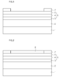
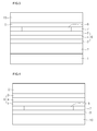
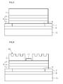
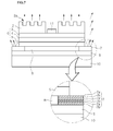
- FIGS. 1 to 6 are sectional views showing a method of manufacturing a light emitting device according to the embodiment.
- a nitride semiconductor layer 2 including a buffer layer is formed on a growth substrate 1, and a light emitting structure 6 including a first conductive semiconductor layer 3, an active layer 4 and a second conductive semiconductor layer 5 is formed on the nitride semiconductor layer 2.
- the nitride semiconductor layer 2 may include an undoped GaN layer
- the light emitting structure 6 may include a GaN-based semiconductor layer.
- the first conductive semiconductor layer 3 may include a group III-V compound semiconductor doped with a first conductive dopant.
- the first conductive semiconductor layer 3 may include GaN, AIN, AlGaN, InGaN, InN, InAlGaN, AlInN, AlGaAs, GaP, GaAs, GaAsP or AlGaInP.
- the first conductive semiconductor layer 3 is an N type semiconductor layer
- the first conductive dopant is an N type dopant, such as Si, Ge, Sn, Se, or Te.
- the first conductive semiconductor layer 3 may have a single layer structure or a multi-layer structure, but the embodiment is not limited thereto.
- the active layer 4 is formed on the first conductive semiconductor layer 3 and may have one of a single quantum well structure, a multiple quantum well (MQW) structure, a quantum dot structure and a quantum wire structure.
- the active layer 4 can be prepared as a well/barrier layer by using group III-V compound semiconductor.
- the active layer 4 may include an InGaN well/GaN barrier layer or an InGaN well/AlGaN barrier layer.
- a clad layer can be interposed between the active layer 4 and the first conductive semiconductor layer 3, or the active layer 4 and the second conductive semiconductor layer 5.
- the clad layer may include an AlGaN-based semiconductor.
- the second conductive semiconductor layer 5 is formed on the active layer 4.
- the second conductive semiconductor layer 5 may include a group III-V compound semiconductor doped with a second conductive dopant.
- the second conductive semiconductor layer 5 may include GaN, AIN, AlGaN, InGaN, InN, InAlGaN, AlInN, AlGaAs, GaP, GaAs, GaAsP or AlGaInP.
- the second conductive semiconductor layer 5 is a P type semiconductor layer
- the second conductive dopant is a P type dopant, such as Mg or Zn.
- the second conductive semiconductor layer 5 may have a single layer structure or a multi-layer structure, but the embodiment is not limited thereto.
- the light emitting structure 6 may further include an N type semiconductor layer on the second conductive semiconductor layer 5.
- the light emitting structure 6 may include at least one of an N-P junction, a P-N junction, an N-P-N junction, and a P-N-P junction.
- An etching protective layer 7 is formed on a peripheral area of the top surface of the second conductive semiconductor layer 5.
- the etching protective layer 7 prevents electric short which is caused as metallic material is splashed to the first conductive semiconductor layer 3, the active layer 4 and the second conductive semiconductor layer 5.
- the etching protective layer 7 can be formed by alternately stacking two mediums having different refractive indexes.
- the etching protective layer 7 effectively reflects light emitted from the active layer 4, thereby improving light efficiency of the light emitting device.
- the etching protective layer 7 will be described later in detail.
- a reflective layer 8 is formed on the second conductive semiconductor layer 5.
- the reflective layer 8 may include at least one of Ag, Al, Ag-Pd-Cu, and Ag-Cu having higher light reflectivity.
- an ohmic contact layer can be formed on the second conductive semiconductor layer 5 for ohmic contact and an adhesive layer can be formed on the ohmic contact layer.
- the reflective layer 8 is formed on the adhesive layer.
- the ohmic contact layer is formed on the second conductive semiconductor layer 5 for ohmic contact and the reflective layer 8 is formed on the ohmic contact layer.
- the ohmic contact layer may include ITO (Indium-Tin-Oxide).
- the ohmic contact layer includes material that permits the ohmic contact with the second conductive semiconductor layer 5.
- the adhesive layer may include AZO (Aluminum-Zinc-Oxide) or IZO (Indium-Zinc-Oxide). Since the adhesive layer includes oxide material, light transmittance can be improved. If the AZO or IZO is used as the adhesive layer, the adhesive layer can be formed with large thickness, so material of the reflective layer 8 can be prevented from diffusing into the light emitting structure. The ohmic contact layer and the adhesive layer can be selectively formed according to material of the reflective layer 8.
- AZO Alluminum-Zinc-Oxide
- IZO Indium-Zinc-Oxide
- a seed layer 9 is formed on the reflective layer 8.
- the seed layer 9 may include one of Au, Cu, Mo, Pt, Sn and W.
- a conductive substrate 10 is formed on the seed layer 9.
- the conductive substrate 10 can be formed by coating copper onto the seed layer 9.
- the conductive substrate 10 may include at least one of Ti, Cu, Cr, Ni, Al, Pt, Au, W, Mo and a semiconductor substrate doped with impurities.
- the growth substrate 1 is removed through an LLO (laser lift off) scheme or a CLO (chemical lift off) scheme.
- the nitride semiconductor layer 2 is also removed. According to the embodiment, only the growth substrate 1 is removed.
- an isolation etching process is performed to separate the light emitting device into chip units.
- the isolation etching process may include an ICP (Induced Coupled Plasma) process. Peripheral portions of the nitride semiconductor layer 2, the first conductive semiconductor layer 3, the active layer 4 and the second conductive semiconductor layer 5 are partially removed through the isolation etching process.
- ICP Induced Coupled Plasma
- the etching protective layer 7 is partially exposed. Due to the etching protective layer 7, particles can be prevented from being generated from the seed layer 9, the bonding layer and the conductive substrate 10 and electric short caused by the particles attached to the light emitting structure 6 can be prevented.
- the nitride semiconductor layer 2 is selectively removed to form an electrode 11 on the first conductive semiconductor layer 3.
- a light extracting structure 2a having a hole shape or a column shape is formed on the top surface of the nitride semiconductor layer 2 in such a manner that the light emitted from the light emitting structure 6 can be effectively extracted upward. In this manner the light emitting device according to the embodiment can be manufactured.
- FIG. 7 is a sectional view showing the light emitting device according to the embodiment.
- the light emitting device shown in FIG. 7 is manufactured through the method shown in FIGS. 1 to 6 .
- the light emitting device includes the conductive substrate 10, on which the seed layer 9 or the bonding layer (not shown) is formed, and the reflective layer 8 is formed on the center portion of the seed layer 9 or the bonding layer.
- the etching protective layer 7 is formed on the peripheral portion of the top surface of the seed layer 9 or the bonding layer.
- the etching protective layer 7 serves as a protective layer to prevent electric short, which is caused as material of the seed layer 9, the bonding layer or the conductive substrate 10 is splashed to the light emitting structure 6.
- the etching protective layer 7 reflects the light emitted from the active layer 4 so that degradation of light efficiency, which is caused due to absorption of light into the seed layer 9, the bonding layer or the conductive substrate 10, can be prevented.
- the etching protective layer 7 includes a first refractive layer 7a having a first refractive index and a second refractive layer 7b having a second refractive index greater than the first refractive index.
- a plurality of first and second refractive layers 7a and 7b are formed alternately and repeatedly. At least one pair of first and second refractive layers 7a and 7b are provided. Preferably, at least two pairs of first and second refractive layers 7a and 7b are provided.
- the first refractive layer 7a may include at least one of SiO 2 , having a refractive index of 1.4 and Al 2 O 3 having a refractive index of 1.7
- the second refractive layer 7b may include at least one of Si having a refractive index of 4.6, Si-H having a refractive index of 3.2, Si 3 N 4 having a refractive index of 2.0, SiN having a refractive index of 2.0, TiO 2 having a refractive index of 2.1 to 2.4 and ZrO 2 having a refractive index of 2.1.
- the etching protective layer 7 may serve as a DBR (Distributed Bragg Reflector) to increase the reflection factor.
- DBR Distributed Bragg Reflector
- a refractive index of the first refractive layer 7a or the second refractive layer 7b is n, and m is odd number
- the first and second refractive layers 7a and 7b of the etching protective layer 7 are stacked at the thickness of m ⁇ /4n to obtain the reflection factor of 95% or above at a specific wavelength A of light.
- the first refractive layer 7a can be formed with a thickness larger than that of the second refractive layer 7b.
- the reflective layer 8 is formed on the seed layer 9 or the bonding layer. At least a part of the reflective layer 8 is surrounded by the etching protective layer 7.
- the reflective layer 8 reflects light, which is emitted from the active layer 4 and directed to the conductive substrate 10, such that the light is directed upward, thereby improving light efficiency of the light emitting device.
- the light emitting structure 6 including the second conductive semiconductor layer 5, the active layer 4 and the first conductive semiconductor layer 3 is formed on the reflective layer 8, and the nitride semiconductor layer 2 having the light extracting structure 2a is formed on the first conductive semiconductor layer 3.
- the electrode 11 is formed on the first conductive semiconductor layer 3.
- a part of light emitted from the light emitting device is directed toward the etching protective layer 7 by passing through a lateral side of the light emitting structure 6.
- the etching protective layer 7 has higher light reflectivity so that the light efficiency of the light emitting device can be improved.
- FIGS. 8 and 9 are graphs showing the reflection factor of an etching protective layer in a light emitting device according to the embodiment
- FIGS. 10 and 11 are graphs showing the reflection factor of an etching protective layer in a light emitting device according to another embodiment.
- the reflection factor of the etching protective layer 7 shown in FIGS. 8 and 9 can be obtained when the first refractive layer 7a having a thickness of 82.14nm and including SiO 2 with a refractive index of 1.4 and the second refractive layer 7b having a thickness of 57.5nm and including SiN with a refractive index of 2.0 are repeatedly formed in the light emitting device that emits light having a wavelength of 460nm.
- the reflection factor is represented in a unit of percentage (%) according to the wavelength of the light emitted from the light emitting device.
- the reflection factor is represented in a unit of percentage (%) according to the number of pairs of the first and second refractive layers 7a and 7b.
- the etching protective layer 7 represents the reflection factor of 90% or above with respect to the light having the wavelength of 400nm to 540nm.
- the reflection factor may increase proportionally to the number of pairs of the first and second refractive layers 7a and 7b.
- the reflection factor of the etching protective layer 7 shown in FIGS. 10 and 11 can be obtained when the first refractive layer 7a having a thickness of 82.14nm and including SiO 2 with a refractive index of 1.4 and the second refractive layer 7b having a thickness of 54.76nm and including TiO 2 with a refractive index of 2.1 are repeatedly formed in the light emitting device that emits light having a wavelength of 460nm.
- the reflection factor is represented in a unit of percentage (%) according to the wavelength of the light emitted from the light emitting device.
- the reflection factor is represented in a unit of percentage (%) according to the number of pairs of the first and second refractive layers 7a and 7b.
- the etching protective layer 7 represents the reflection factor of 90% or above with respect to the light having the wavelength of 400nm to 540nm.
- the reflection factor may increase proportionally to the number of pairs of the first and second refractive layers 7a and 7b.
- the light emitting device includes the etching protective layer 7 so that the light efficiency can be improved.
- FIG. 12 is a sectional view showing a light emitting device package including the light emitting device according to the embodiments.
- the light emitting device package includes a package body 30, first and second electrodes 31 and 32 installed in the package body 30, a light emitting device 100 installed in the package body 30 and electrically connected to the first and second electrodes 31 and 32, and an encapsulating layer 40 surrounding the light emitting device 100.
- the package body 30 may include silicon, synthetic resin or metal and may have a cavity with an inclined lateral side.
- the first and second electrodes 31 and 32 are electrically separated from each other and supply power to the light emitting device 100.
- the first and second electrodes 31 and 32 reflect the light emitted from the light emitting device 100 to improve the light efficiency and dissipate heat generated from the light emitting device 100 to the outside.
- the light emitting device as shown in FIG. 7 can be used as the light emitting device 100.
- the light emitting device 100 can be installed on the package body 30, the first electrode 31 or the second electrode 32.
- the light emitting device 100 can be electrically connected to the first and second electrodes 31 and 32 through a wiring scheme, a flip chip scheme or a die bonding scheme. According to the embodiment, the light emitting device 100 is electrically connected to the first electrode 31 through a wire 50 while directly making contact with the second electrode 32.
- the encapsulating layer 40 surrounds the light emitting device 100 to protect the light emitting device 100.
- the encapsulating layer 40 may include a phosphor to vary the wavelength of the light emitted from the light emitting device 100.
- the light emitting apparatus may include at least one light emitting device according to the embodiment.
- the embodiment may not limit the number of the light emitting devices.
- a plurality of light emitting device package according to the embodiment can be arranged on the substrate.
- optical members such as a light guide plate, a prism sheet and a diffusion sheet, can be arranged in a path of light emitted from the light emitting device package.
- the light emitting device package, the substrate, the optical members may serve as a lighting device.
- a display device, an indicating device, or a lighting system can be established by using the light emitting device or the light emitting device package.
- the lighting system may include a lamp or a street lamp.
- any reference in this specification to "one embodiment,” “an embodiment,” “example embodiment,” etc. means that a particular feature, structure, or characteristic described in connection with the embodiment is included in at least one embodiment of the invention.
- the appearances of such phrases in various places in the specification are not necessarily all referring to the same embodiment.
Landscapes
- Led Devices (AREA)
Abstract
Description
- The present application claims priority of Korean Patent Application No.
10-2009-0020134 filed on March 10, 2009 - The embodiment relates to a light emitting device, a method of manufacturing the same, and a light emitting apparatus.
- A light emitting diode includes a light emitting structure having a first conductive semiconductor layer, an active layer and a second conductive semiconductor layer and the light emitting structure emits light as power is applied thereto.
- The light emitting structure is formed on a growth substrate, such as a sapphire substrate, as an epitaxial layer, and a reflective layer is formed on the light emitting structure. Then, a conductive substrate is formed on the reflective layer and the growth substrate is removed, thereby obtaining a vertical type light emitting diode.
- The embodiment provides a light emitting device having an improved structure, a method of manufacturing the same and a light emitting apparatus.
- The embodiment provides a light emitting device capable of improving light efficiency, a method of manufacturing the same and a light emitting apparatus.
- According to the embodiment, there is provided a light emitting device comprising: a conductive substrate; a reflective layer on the conductive substrate; an etching protective layer on a peripheral portion of a top surface of the conductive substrate; and a light emitting structure, which is formed on the reflective layer and the etching protective layer such that the etching protective layer is partially exposed and includes a first conductive semiconductor layer, a second conductive semiconductor layer and an active layer between the first and second conductive semiconductor layers, wherein the etching protective layer includes a first refractive layer having a first refractive index and a second refractive layer having a second refractive index greater than the first refractive index.
- According to the embodiment, there is provided a light emitting device package comprising: a package body; a light emitting device on the package body; an electrode electrically connected to the light emitting device; and an encapsulating layer surrounding the light emitting device. The light emitting device comprises: a conductive substrate; a reflective layer on the conductive substrate; an etching protective layer on a peripheral portion of a top surface of the conductive substrate; and a light emitting structure, which is formed on the reflective layer and the etching protective layer such that the etching protective layer is partially exposed, wherein the etching protective layer includes a first refractive layer having a first refractive index and a second refractive layer having a second refractive index greater than the first refractive index.
- According to the embodiment, there is provided a lighting system comprising: a light emitting device package including a package body, a light emitting device on the package body, an electrode electrically connected to the light emitting device, and an encapsulating layer surrounding the light emitting device. The light emitting device comprises: a conductive substrate; a reflective layer on the conductive substrate; an etching protective layer on a peripheral portion of a top surface of the conductive substrate; and a light emitting structure, which is formed on the reflective layer and the etching protective layer such that the etching protective layer is partially exposed, wherein the etching protective layer includes a first refractive layer having a first refractive index and a second refractive layer having a second refractive index greater than the first refractive index.
-
-
FIGS. 1 to 6 are sectional views showing a method of manufacturing a light emitting device according to the embodiment; -
FIG. 7 is a sectional view showing a light emitting device according to the embodiment; -
FIGS. 8 and 9 are graphs showing the reflection factor of an etching protective layer in a light emitting device according to the embodiment; -
FIGS. 10 and 11 are graphs showing the reflection factor of an etching protective layer in a light emitting device according to another embodiment; and -
FIG. 12 is a view showing a light emitting apparatus according to the embodiment. - In the description of the embodiments, it will be understood that, when a layer (or film), a region, a pattern, or a structure is referred to as being "on" or "under" another substrate, another layer (or film), another region, another pad, or another pattern, it can be "directly" or "indirectly" on the other substrate, layer (or film), region, pad, or pattern, or one or more intervening layers may also be present. Such a position of the layer has been described with reference to the drawings.
- The thickness and size of each layer shown in the drawings can be exaggerated, omitted or schematically drawn for the purpose of convenience or clarity. In addition, the size of elements does not utterly reflect an actual size.
-
FIGS. 1 to 6 are sectional views showing a method of manufacturing a light emitting device according to the embodiment. - Referring to
FIG. 1 , anitride semiconductor layer 2 including a buffer layer is formed on agrowth substrate 1, and alight emitting structure 6 including a firstconductive semiconductor layer 3, anactive layer 4 and a secondconductive semiconductor layer 5 is formed on thenitride semiconductor layer 2. - Various substrates, such as Al2O3, Si, SiC, GaAs, ZnO, and MgO substrates, can be used as the
growth substrate 1. Thenitride semiconductor layer 2 may include an undoped GaN layer, and thelight emitting structure 6 may include a GaN-based semiconductor layer. - The first
conductive semiconductor layer 3 may include a group III-V compound semiconductor doped with a first conductive dopant. For instance, the firstconductive semiconductor layer 3 may include GaN, AIN, AlGaN, InGaN, InN, InAlGaN, AlInN, AlGaAs, GaP, GaAs, GaAsP or AlGaInP. If the firstconductive semiconductor layer 3 is an N type semiconductor layer, the first conductive dopant is an N type dopant, such as Si, Ge, Sn, Se, or Te. The firstconductive semiconductor layer 3 may have a single layer structure or a multi-layer structure, but the embodiment is not limited thereto. - The
active layer 4 is formed on the firstconductive semiconductor layer 3 and may have one of a single quantum well structure, a multiple quantum well (MQW) structure, a quantum dot structure and a quantum wire structure. Theactive layer 4 can be prepared as a well/barrier layer by using group III-V compound semiconductor. For instance, theactive layer 4 may include an InGaN well/GaN barrier layer or an InGaN well/AlGaN barrier layer. - A clad layer can be interposed between the
active layer 4 and the firstconductive semiconductor layer 3, or theactive layer 4 and the secondconductive semiconductor layer 5. The clad layer may include an AlGaN-based semiconductor. - The second
conductive semiconductor layer 5 is formed on theactive layer 4. The secondconductive semiconductor layer 5 may include a group III-V compound semiconductor doped with a second conductive dopant. For instance, the secondconductive semiconductor layer 5 may include GaN, AIN, AlGaN, InGaN, InN, InAlGaN, AlInN, AlGaAs, GaP, GaAs, GaAsP or AlGaInP. If the secondconductive semiconductor layer 5 is a P type semiconductor layer, the second conductive dopant is a P type dopant, such as Mg or Zn. The secondconductive semiconductor layer 5 may have a single layer structure or a multi-layer structure, but the embodiment is not limited thereto. - Meanwhile, the
light emitting structure 6 may further include an N type semiconductor layer on the secondconductive semiconductor layer 5. For instance, thelight emitting structure 6 may include at least one of an N-P junction, a P-N junction, an N-P-N junction, and a P-N-P junction. - An etching
protective layer 7 is formed on a peripheral area of the top surface of the secondconductive semiconductor layer 5. - When the isolation etching is performed to separate the light emitting device into a chip unit, the etching
protective layer 7 prevents electric short which is caused as metallic material is splashed to the firstconductive semiconductor layer 3, theactive layer 4 and the secondconductive semiconductor layer 5. - The etching
protective layer 7 can be formed by alternately stacking two mediums having different refractive indexes. The etchingprotective layer 7 effectively reflects light emitted from theactive layer 4, thereby improving light efficiency of the light emitting device. The etchingprotective layer 7 will be described later in detail. - Referring to
FIG. 2 , areflective layer 8 is formed on the secondconductive semiconductor layer 5. - The
reflective layer 8 may include at least one of Ag, Al, Ag-Pd-Cu, and Ag-Cu having higher light reflectivity. - Although not shown in the drawings, an ohmic contact layer can be formed on the second
conductive semiconductor layer 5 for ohmic contact and an adhesive layer can be formed on the ohmic contact layer. In this case, thereflective layer 8 is formed on the adhesive layer. Otherwise, the ohmic contact layer is formed on the secondconductive semiconductor layer 5 for ohmic contact and thereflective layer 8 is formed on the ohmic contact layer. - For instance, the ohmic contact layer may include ITO (Indium-Tin-Oxide). The ohmic contact layer includes material that permits the ohmic contact with the second
conductive semiconductor layer 5. - The adhesive layer may include AZO (Aluminum-Zinc-Oxide) or IZO (Indium-Zinc-Oxide). Since the adhesive layer includes oxide material, light transmittance can be improved. If the AZO or IZO is used as the adhesive layer, the adhesive layer can be formed with large thickness, so material of the
reflective layer 8 can be prevented from diffusing into the light emitting structure. The ohmic contact layer and the adhesive layer can be selectively formed according to material of thereflective layer 8. - Referring to
FIG. 3 , aseed layer 9 is formed on thereflective layer 8. Theseed layer 9 may include one of Au, Cu, Mo, Pt, Sn and W. Aconductive substrate 10 is formed on theseed layer 9. For instance, theconductive substrate 10 can be formed by coating copper onto theseed layer 9. - Instead of forming the
seed layer 9 on thereflective layer 8, a bonding layer (not shown) can be formed on thereflective layer 8 to bond theconductive substrate 10 with thereflective layer 8. In this case, theconductive substrate 10 may include at least one of Ti, Cu, Cr, Ni, Al, Pt, Au, W, Mo and a semiconductor substrate doped with impurities. - Referring to
FIG. 4 , in the structure shown inFIG. 3 , thegrowth substrate 1 is removed through an LLO (laser lift off) scheme or a CLO (chemical lift off) scheme. At this time, thenitride semiconductor layer 2 is also removed. According to the embodiment, only thegrowth substrate 1 is removed. - Referring to
FIG. 5 , an isolation etching process is performed to separate the light emitting device into chip units. The isolation etching process may include an ICP (Induced Coupled Plasma) process. Peripheral portions of thenitride semiconductor layer 2, the firstconductive semiconductor layer 3, theactive layer 4 and the secondconductive semiconductor layer 5 are partially removed through the isolation etching process. - At this time, the etching
protective layer 7 is partially exposed. Due to the etchingprotective layer 7, particles can be prevented from being generated from theseed layer 9, the bonding layer and theconductive substrate 10 and electric short caused by the particles attached to thelight emitting structure 6 can be prevented. - Referring to
FIG. 6 , thenitride semiconductor layer 2 is selectively removed to form anelectrode 11 on the firstconductive semiconductor layer 3. In addition, alight extracting structure 2a having a hole shape or a column shape is formed on the top surface of thenitride semiconductor layer 2 in such a manner that the light emitted from thelight emitting structure 6 can be effectively extracted upward. In this manner the light emitting device according to the embodiment can be manufactured. -
FIG. 7 is a sectional view showing the light emitting device according to the embodiment. - The light emitting device shown in
FIG. 7 is manufactured through the method shown inFIGS. 1 to 6 . - The light emitting device includes the
conductive substrate 10, on which theseed layer 9 or the bonding layer (not shown) is formed, and thereflective layer 8 is formed on the center portion of theseed layer 9 or the bonding layer. In addition, the etchingprotective layer 7 is formed on the peripheral portion of the top surface of theseed layer 9 or the bonding layer. - When the isolation etching process is performed for the light emitting device, the etching
protective layer 7 serves as a protective layer to prevent electric short, which is caused as material of theseed layer 9, the bonding layer or theconductive substrate 10 is splashed to thelight emitting structure 6. In addition, the etchingprotective layer 7 reflects the light emitted from theactive layer 4 so that degradation of light efficiency, which is caused due to absorption of light into theseed layer 9, the bonding layer or theconductive substrate 10, can be prevented. - The etching
protective layer 7 includes a firstrefractive layer 7a having a first refractive index and a secondrefractive layer 7b having a second refractive index greater than the first refractive index. A plurality of first and secondrefractive layers refractive layers refractive layers - The first
refractive layer 7a may include at least one of SiO2, having a refractive index of 1.4 and Al2O3 having a refractive index of 1.7, and the secondrefractive layer 7b may include at least one of Si having a refractive index of 4.6, Si-H having a refractive index of 3.2, Si3N4 having a refractive index of 2.0, SiN having a refractive index of 2.0, TiO2 having a refractive index of 2.1 to 2.4 and ZrO2 having a refractive index of 2.1. - The etching
protective layer 7 may serve as a DBR (Distributed Bragg Reflector) to increase the reflection factor. - When a wavelength of light emitted from the light emitting device is A, a refractive index of the first
refractive layer 7a or the secondrefractive layer 7b is n, and m is odd number, the first and secondrefractive layers protective layer 7 are stacked at the thickness of mλ/4n to obtain the reflection factor of 95% or above at a specific wavelength A of light. For instance, the firstrefractive layer 7a can be formed with a thickness larger than that of the secondrefractive layer 7b. - Meanwhile, the
reflective layer 8 is formed on theseed layer 9 or the bonding layer. At least a part of thereflective layer 8 is surrounded by the etchingprotective layer 7. Thereflective layer 8 reflects light, which is emitted from theactive layer 4 and directed to theconductive substrate 10, such that the light is directed upward, thereby improving light efficiency of the light emitting device. - The
light emitting structure 6 including the secondconductive semiconductor layer 5, theactive layer 4 and the firstconductive semiconductor layer 3 is formed on thereflective layer 8, and thenitride semiconductor layer 2 having thelight extracting structure 2a is formed on the firstconductive semiconductor layer 3. In addition, theelectrode 11 is formed on the firstconductive semiconductor layer 3. - As indicated by an arrow in
FIG. 7 , a part of light emitted from the light emitting device is directed toward the etchingprotective layer 7 by passing through a lateral side of thelight emitting structure 6. As mentioned above, the etchingprotective layer 7 has higher light reflectivity so that the light efficiency of the light emitting device can be improved. -
FIGS. 8 and 9 are graphs showing the reflection factor of an etching protective layer in a light emitting device according to the embodiment, andFIGS. 10 and 11 are graphs showing the reflection factor of an etching protective layer in a light emitting device according to another embodiment. - Referring to
FIGS. 8 and 9 , the reflection factor of the etchingprotective layer 7 shown inFIGS. 8 and 9 can be obtained when the firstrefractive layer 7a having a thickness of 82.14nm and including SiO2 with a refractive index of 1.4 and the secondrefractive layer 7b having a thickness of 57.5nm and including SiN with a refractive index of 2.0 are repeatedly formed in the light emitting device that emits light having a wavelength of 460nm. - Referring to
FIG. 8 , the reflection factor is represented in a unit of percentage (%) according to the wavelength of the light emitted from the light emitting device. Referring toFIG. 9 , the reflection factor is represented in a unit of percentage (%) according to the number of pairs of the first and secondrefractive layers - As shown in
FIG. 8 , the etchingprotective layer 7 represents the reflection factor of 90% or above with respect to the light having the wavelength of 400nm to 540nm. In addition, as shown inFIG. 9 , the reflection factor may increase proportionally to the number of pairs of the first and secondrefractive layers - Referring to
FIGS. 10 and 11 , the reflection factor of the etchingprotective layer 7 shown inFIGS. 10 and 11 can be obtained when the firstrefractive layer 7a having a thickness of 82.14nm and including SiO2 with a refractive index of 1.4 and the secondrefractive layer 7b having a thickness of 54.76nm and including TiO2 with a refractive index of 2.1 are repeatedly formed in the light emitting device that emits light having a wavelength of 460nm. - Referring to
FIG. 10 , the reflection factor is represented in a unit of percentage (%) according to the wavelength of the light emitted from the light emitting device. Referring toFIG. 11 , the reflection factor is represented in a unit of percentage (%) according to the number of pairs of the first and secondrefractive layers - As shown in
FIG. 10 , the etchingprotective layer 7 represents the reflection factor of 90% or above with respect to the light having the wavelength of 400nm to 540nm. In addition, as shown inFIG. 11 , the reflection factor may increase proportionally to the number of pairs of the first and secondrefractive layers - As described above, the light emitting device according to the embodiment includes the etching
protective layer 7 so that the light efficiency can be improved. -
FIG. 12 is a sectional view showing a light emitting device package including the light emitting device according to the embodiments. - Referring to
FIG. 12 , the light emitting device package according to the embodiments includes apackage body 30, first andsecond electrodes package body 30, alight emitting device 100 installed in thepackage body 30 and electrically connected to the first andsecond electrodes encapsulating layer 40 surrounding thelight emitting device 100. - The
package body 30 may include silicon, synthetic resin or metal and may have a cavity with an inclined lateral side. - The first and
second electrodes light emitting device 100. In addition, the first andsecond electrodes light emitting device 100 to improve the light efficiency and dissipate heat generated from thelight emitting device 100 to the outside. - The light emitting device as shown in
FIG. 7 can be used as thelight emitting device 100. Thelight emitting device 100 can be installed on thepackage body 30, thefirst electrode 31 or thesecond electrode 32. - The
light emitting device 100 can be electrically connected to the first andsecond electrodes light emitting device 100 is electrically connected to thefirst electrode 31 through awire 50 while directly making contact with thesecond electrode 32. - The encapsulating
layer 40 surrounds thelight emitting device 100 to protect thelight emitting device 100. In addition, the encapsulatinglayer 40 may include a phosphor to vary the wavelength of the light emitted from thelight emitting device 100. - The light emitting apparatus may include at least one light emitting device according to the embodiment. The embodiment may not limit the number of the light emitting devices.
- A plurality of light emitting device package according to the embodiment can be arranged on the substrate. In addition, optical members, such as a light guide plate, a prism sheet and a diffusion sheet, can be arranged in a path of light emitted from the light emitting device package. The light emitting device package, the substrate, the optical members may serve as a lighting device. According to another embodiment, a display device, an indicating device, or a lighting system can be established by using the light emitting device or the light emitting device package. For instance, the lighting system may include a lamp or a street lamp.
- Any reference in this specification to "one embodiment," "an embodiment," "example embodiment," etc., means that a particular feature, structure, or characteristic described in connection with the embodiment is included in at least one embodiment of the invention. The appearances of such phrases in various places in the specification are not necessarily all referring to the same embodiment. Further, when a particular feature, structure, or characteristic is described in connection with any embodiment, it is submitted that it is within the purview of one skilled in the art to effect such feature, structure, or characteristic in connection with other ones of the embodiments.
- Although embodiments have been described with reference to a number of illustrative embodiments thereof, it should be understood that numerous other modifications and embodiments can be devised by those skilled in the art that will fall within the spirit and scope of the principles of this disclosure. More particularly, various variations and modifications are possible in the component parts and/or arrangements of the subject combination arrangement within the scope of the disclosure, the drawings and the appended claims. In addition to variations and modifications in the component parts and/or arrangements, alternative uses will also be apparent to those skilled in the art.
Claims (14)
- A light emitting device comprising:a conductive substrate;a reflective layer on the conductive substrate;an etching protective layer on a peripheral portion of a top surface of the conductive substrate; anda light emitting structure, which is formed on the reflective layer and the etching protective layer such that the etching protective layer is partially exposed and includes a first conductive semiconductor layer, a second conductive semiconductor layer and an active layer between the first and second conductive semiconductor layers,wherein the etching protective layer includes a first refractive layer having a first refractive index and a second refractive layer having a second refractive index greater than the first refractive index.
- The light emitting device of claim 1, wherein the etching protective layer overlaps with the conductive substrate and partially overlaps with the light emitting structure in a vertical direction.
- The light emitting device of claim 1, wherein the first and second refractive layers are stacked alternately.
- The light emitting device of claim 1, wherein the first refractive layer includes at least one of SiO2 and Al2O3.
- The light emitting device of claim 1, wherein the second refractive layer includes at least one of Si, Si-H, Si3N4, SiN, TiO2 and ZrO2.
- The light emitting device of claim 1, further comprising a seed layer or a bonding layer between the conductive substrate and the reflective layer.
- The light emitting device of claim 1, further comprising at least one of an ohmic contact layer and an adhesive layer between the reflective layer and the light emitting structure.
- The light emitting device of claim 1, further comprising a nitride semiconductor layer having a light extraction structure on the light emitting structure.
- The light emitting device of claim 1, wherein at least two pairs of first and second refractive layers are provided.
- The light emitting device of claim 1, wherein the first and second refractive layers have thickness of mλ/4n respectively, in which A is a wavelength of light emitted from the light emitting structure, n is a refractive index of the first refractive layer or the second refractive layer, and m is an odd number.
- The light emitting device of claim 1, wherein the first refractive layer is thicker than the second refractive layer.
- A light emitting device package comprising:a package body;a light emitting device on the package body;an electrode electrically connected to the light emitting device; andan encapsulating layer surrounding the light emitting device,wherein the light emitting device comprises:a conductive substrate;a reflective layer on the conductive substrate;an etching protective layer on a peripheral portion of a top surface of the conductive substrate; anda light emitting structure, which is formed on the reflective layer and the etching protective layer such that the etching protective layer is partially exposed,wherein the etching protective layer includes a first refractive layer having a first refractive index and a second refractive layer having a second refractive index greater than the first refractive index.
- A method of manufacturing a light emitting device, the method comprising:forming a light emitting structure including a first conductive semiconductor layer, an active layer and a second conductive semiconductor layer on a growth substrate;forming a reflective layer and an etching protective layer on the light emitting structure;forming a conductive substrate on the reflective layer and the etching protective layer;removing the growth substrate and removing the light emitting structure such that the etching protective layer is partially exposed; andforming an electrode on the first conductive semiconductor layer,wherein he etching protective layer includes a first refractive layer having a first refractive index and a second refractive layer having a second refractive index greater than the first refractive index.
- A lighting system comprising:a light emitting device package including a package body, a light emitting device on the package body, an electrode electrically connected to the light emitting device, and an encapsulating layer surrounding the light emitting device,wherein the light emitting device comprises:a conductive substrate;a reflective layer on the conductive substrate;an etching protective layer on a peripheral portion of a top surface of the conductive substrate; anda light emitting structure, which is formed on the reflective layer and the etching protective layer such that the etching protective layer is partially exposed,wherein the etching protective layer includes a first refractive layer having a first refractive index and a second refractive layer having a second refractive index greater than the first refractive index.
Applications Claiming Priority (1)
| Application Number | Priority Date | Filing Date | Title |
|---|---|---|---|
| KR1020090020134A KR101550922B1 (en) | 2009-03-10 | 2009-03-10 | Light emitting element |
Publications (2)
| Publication Number | Publication Date |
|---|---|
| EP2228840A1 true EP2228840A1 (en) | 2010-09-15 |
| EP2228840B1 EP2228840B1 (en) | 2017-12-06 |
Family
ID=42224859
Family Applications (1)
| Application Number | Title | Priority Date | Filing Date |
|---|---|---|---|
| EP10155814.6A Not-in-force EP2228840B1 (en) | 2009-03-10 | 2010-03-08 | Light emitting device, light emitting device package, and lighting system |
Country Status (4)
| Country | Link |
|---|---|
| US (1) | US8637884B2 (en) |
| EP (1) | EP2228840B1 (en) |
| KR (1) | KR101550922B1 (en) |
| CN (1) | CN101834255B (en) |
Families Citing this family (9)
| Publication number | Priority date | Publication date | Assignee | Title |
|---|---|---|---|---|
| KR101154511B1 (en) * | 2010-10-18 | 2012-06-13 | 서울옵토디바이스주식회사 | High efficiency light emitting diode and method of fabricating the same |
| TWI458133B (en) * | 2011-09-06 | 2014-10-21 | 新世紀光電股份有限公司 | Substrate |
| CN105140375A (en) * | 2011-09-29 | 2015-12-09 | 新世纪光电股份有限公司 | Substrate and Light Emitting Diode Device |
| CN103117337B (en) * | 2013-01-31 | 2015-11-11 | 圆融光电科技有限公司 | A kind of patterned substrate preparation method |
| CN103187499B (en) * | 2013-03-07 | 2015-11-25 | 天津三安光电有限公司 | Light-emitting Diode And Its Making Method |
| CN104282813B (en) * | 2013-07-02 | 2018-04-06 | 晶元光电股份有限公司 | Light emitting element |
| CN103728683A (en) * | 2013-12-25 | 2014-04-16 | 京东方科技集团股份有限公司 | Display substrate and manufacturing method thereof |
| KR102410788B1 (en) * | 2015-06-30 | 2022-06-21 | 쑤저우 레킨 세미컨덕터 컴퍼니 리미티드 | Light emitting device |
| US10698158B1 (en) * | 2017-11-28 | 2020-06-30 | Facebook Technologies, Llc | Optical waveguides in micro-LED devices |
Citations (3)
| Publication number | Priority date | Publication date | Assignee | Title |
|---|---|---|---|---|
| US20030141506A1 (en) * | 2002-01-28 | 2003-07-31 | Masahiko Sano | Nitride semiconductor element with a supporting substrate and a method for producing a nitride semiconductor element |
| US20070114552A1 (en) * | 2005-11-23 | 2007-05-24 | Samsung Electro-Mechanics Co., Ltd. | Vertical gallium-nitride based light emitting diode |
| DE102007029370A1 (en) * | 2007-05-04 | 2008-11-06 | Osram Opto Semiconductors Gmbh | Semiconductor chip and method for producing a semiconductor chip |
Family Cites Families (12)
| Publication number | Priority date | Publication date | Assignee | Title |
|---|---|---|---|---|
| US5078006A (en) * | 1990-08-30 | 1992-01-07 | Vista Research, Inc. | Methods for detection of leaks in pressurized pipeline systems |
| JP3644927B2 (en) * | 2000-03-17 | 2005-05-11 | 松下電器産業株式会社 | Surface emitting device |
| US7088038B2 (en) * | 2003-07-02 | 2006-08-08 | Gelcore Llc | Green phosphor for general illumination applications |
| JP2005277372A (en) * | 2004-02-25 | 2005-10-06 | Sanken Electric Co Ltd | Semiconductor light emitting device and manufacturing method thereof |
| US7352006B2 (en) * | 2004-09-28 | 2008-04-01 | Goldeneye, Inc. | Light emitting diodes exhibiting both high reflectivity and high light extraction |
| US7432119B2 (en) * | 2005-01-11 | 2008-10-07 | Semileds Corporation | Light emitting diode with conducting metal substrate |
| US20070018182A1 (en) * | 2005-07-20 | 2007-01-25 | Goldeneye, Inc. | Light emitting diodes with improved light extraction and reflectivity |
| JP4933130B2 (en) * | 2006-02-16 | 2012-05-16 | 昭和電工株式会社 | GaN-based semiconductor light-emitting device and manufacturing method thereof |
| JP2007281081A (en) * | 2006-04-04 | 2007-10-25 | Rohm Co Ltd | Semiconductor light emitting device |
| WO2007148866A1 (en) * | 2006-06-23 | 2007-12-27 | Lg Electronics Inc. | Light emitting diode having vertical topology and method of making the same |
| DE602007012890D1 (en) | 2006-07-28 | 2011-04-14 | Chromogenics Sweden Ab | CONTACTING ELECTROCHROMICAL ARRANGEMENTS |
| KR101449005B1 (en) * | 2007-11-26 | 2014-10-08 | 엘지이노텍 주식회사 | Semiconductor light emitting device and manufacturing method thereof |
-
2009
- 2009-03-10 KR KR1020090020134A patent/KR101550922B1/en not_active Expired - Fee Related
-
2010
- 2010-03-08 EP EP10155814.6A patent/EP2228840B1/en not_active Not-in-force
- 2010-03-09 US US12/720,059 patent/US8637884B2/en not_active Expired - Fee Related
- 2010-03-10 CN CN2010101357677A patent/CN101834255B/en active Active
Patent Citations (3)
| Publication number | Priority date | Publication date | Assignee | Title |
|---|---|---|---|---|
| US20030141506A1 (en) * | 2002-01-28 | 2003-07-31 | Masahiko Sano | Nitride semiconductor element with a supporting substrate and a method for producing a nitride semiconductor element |
| US20070114552A1 (en) * | 2005-11-23 | 2007-05-24 | Samsung Electro-Mechanics Co., Ltd. | Vertical gallium-nitride based light emitting diode |
| DE102007029370A1 (en) * | 2007-05-04 | 2008-11-06 | Osram Opto Semiconductors Gmbh | Semiconductor chip and method for producing a semiconductor chip |
Also Published As
| Publication number | Publication date |
|---|---|
| KR20100101772A (en) | 2010-09-20 |
| CN101834255B (en) | 2013-03-27 |
| CN101834255A (en) | 2010-09-15 |
| KR101550922B1 (en) | 2015-09-07 |
| EP2228840B1 (en) | 2017-12-06 |
| US20100230702A1 (en) | 2010-09-16 |
| US8637884B2 (en) | 2014-01-28 |
Similar Documents
| Publication | Publication Date | Title |
|---|---|---|
| KR101627010B1 (en) | Semiconductor light emitting device including metal reflecting layer | |
| KR100986353B1 (en) | Light emitting device, method for fabricating the light emitting device and light emitting device package | |
| EP2228840B1 (en) | Light emitting device, light emitting device package, and lighting system | |
| KR101039999B1 (en) | Semiconductor light emitting device and manufacturing method thereof | |
| KR101014071B1 (en) | Light emitting device, light emitting device manufacturing method, light emitting device package and lighting system | |
| CN102456795B (en) | Light emitting device | |
| KR100986523B1 (en) | Semiconductor light emitting device and fabrication method thereof | |
| KR100986374B1 (en) | Light emitting device, method for fabricating the light emitting device and light emitting device package | |
| KR101034144B1 (en) | Light emitting device, light emitting device manufacturing method, light emitting device package and lighting system | |
| CN108040503B (en) | Light emitting device | |
| EP2219238B1 (en) | Semiconductor light-emitting device | |
| KR102250516B1 (en) | Light emitting device | |
| EP2328189B1 (en) | Semiconductor light emitting device | |
| KR20150141790A (en) | Light emitting deviceand light emitting device package thereof | |
| US8049241B2 (en) | Light emitting device fabrication method thereof, and light emitting apparatus | |
| KR20110118333A (en) | Light emitting device, light emitting device manufacturing method, light emitting device package, and lighting system | |
| KR101776302B1 (en) | Light emitting device and light emitting device package | |
| KR20120042516A (en) | Light emitting device, method for fabricating the light emitting device, light emitting device package and lighting system | |
| KR102510591B1 (en) | Light emitting device and light emitting device package | |
| KR102249637B1 (en) | Light emitting device and light emitting device package thereof | |
| KR20120045636A (en) | Light emitting device, method for fabricating the light emitting device, light emitting device package and lighting system | |
| KR20110118380A (en) | Light emitting device, light emitting device manufacturing method, light emitting device package, lighting system | |
| KR20120088046A (en) | Light emitting device, method for fabricating the light emitting device, light emitting device package and lighting system |
Legal Events
| Date | Code | Title | Description |
|---|---|---|---|
| PUAI | Public reference made under article 153(3) epc to a published international application that has entered the european phase |
Free format text: ORIGINAL CODE: 0009012 |
|
| 17P | Request for examination filed |
Effective date: 20100308 |
|
| AK | Designated contracting states |
Kind code of ref document: A1 Designated state(s): AT BE BG CH CY CZ DE DK EE ES FI FR GB GR HR HU IE IS IT LI LT LU LV MC MK MT NL NO PL PT RO SE SI SK SM TR |
|
| AX | Request for extension of the european patent |
Extension state: AL BA ME RS |
|
| RAP1 | Party data changed (applicant data changed or rights of an application transferred) |
Owner name: LG INNOTEK CO., LTD. |
|
| RAP1 | Party data changed (applicant data changed or rights of an application transferred) |
Owner name: LG INNOTEK CO., LTD. |
|
| RAP1 | Party data changed (applicant data changed or rights of an application transferred) |
Owner name: LG INNOTEK CO., LTD. |
|
| GRAP | Despatch of communication of intention to grant a patent |
Free format text: ORIGINAL CODE: EPIDOSNIGR1 |
|
| STAA | Information on the status of an ep patent application or granted ep patent |
Free format text: STATUS: GRANT OF PATENT IS INTENDED |
|
| RIC1 | Information provided on ipc code assigned before grant |
Ipc: H01L 33/20 20100101ALN20170602BHEP Ipc: H01L 33/46 20100101AFI20170602BHEP Ipc: H01L 33/00 20100101ALN20170602BHEP |
|
| RIC1 | Information provided on ipc code assigned before grant |
Ipc: H01L 33/20 20100101ALN20170621BHEP Ipc: H01L 33/46 20100101AFI20170621BHEP Ipc: H01L 33/00 20100101ALN20170621BHEP |
|
| INTG | Intention to grant announced |
Effective date: 20170705 |
|
| GRAS | Grant fee paid |
Free format text: ORIGINAL CODE: EPIDOSNIGR3 |
|
| GRAA | (expected) grant |
Free format text: ORIGINAL CODE: 0009210 |
|
| STAA | Information on the status of an ep patent application or granted ep patent |
Free format text: STATUS: THE PATENT HAS BEEN GRANTED |
|
| AK | Designated contracting states |
Kind code of ref document: B1 Designated state(s): AT BE BG CH CY CZ DE DK EE ES FI FR GB GR HR HU IE IS IT LI LT LU LV MC MK MT NL NO PL PT RO SE SI SK SM TR |
|
| REG | Reference to a national code |
Ref country code: GB Ref legal event code: FG4D |
|
| REG | Reference to a national code |
Ref country code: AT Ref legal event code: REF Ref document number: 953117 Country of ref document: AT Kind code of ref document: T Effective date: 20171215 Ref country code: CH Ref legal event code: EP |
|
| REG | Reference to a national code |
Ref country code: IE Ref legal event code: FG4D |
|
| REG | Reference to a national code |
Ref country code: DE Ref legal event code: R096 Ref document number: 602010047120 Country of ref document: DE |
|
| REG | Reference to a national code |
Ref country code: NL Ref legal event code: FP |
|
| REG | Reference to a national code |
Ref country code: FR Ref legal event code: PLFP Year of fee payment: 9 |
|
| REG | Reference to a national code |
Ref country code: LT Ref legal event code: MG4D |
|
| PG25 | Lapsed in a contracting state [announced via postgrant information from national office to epo] |
Ref country code: ES Free format text: LAPSE BECAUSE OF FAILURE TO SUBMIT A TRANSLATION OF THE DESCRIPTION OR TO PAY THE FEE WITHIN THE PRESCRIBED TIME-LIMIT Effective date: 20171206 Ref country code: SE Free format text: LAPSE BECAUSE OF FAILURE TO SUBMIT A TRANSLATION OF THE DESCRIPTION OR TO PAY THE FEE WITHIN THE PRESCRIBED TIME-LIMIT Effective date: 20171206 Ref country code: FI Free format text: LAPSE BECAUSE OF FAILURE TO SUBMIT A TRANSLATION OF THE DESCRIPTION OR TO PAY THE FEE WITHIN THE PRESCRIBED TIME-LIMIT Effective date: 20171206 Ref country code: LT Free format text: LAPSE BECAUSE OF FAILURE TO SUBMIT A TRANSLATION OF THE DESCRIPTION OR TO PAY THE FEE WITHIN THE PRESCRIBED TIME-LIMIT Effective date: 20171206 Ref country code: NO Free format text: LAPSE BECAUSE OF FAILURE TO SUBMIT A TRANSLATION OF THE DESCRIPTION OR TO PAY THE FEE WITHIN THE PRESCRIBED TIME-LIMIT Effective date: 20180306 |
|
| REG | Reference to a national code |
Ref country code: AT Ref legal event code: MK05 Ref document number: 953117 Country of ref document: AT Kind code of ref document: T Effective date: 20171206 |
|
| PG25 | Lapsed in a contracting state [announced via postgrant information from national office to epo] |
Ref country code: GR Free format text: LAPSE BECAUSE OF FAILURE TO SUBMIT A TRANSLATION OF THE DESCRIPTION OR TO PAY THE FEE WITHIN THE PRESCRIBED TIME-LIMIT Effective date: 20180307 Ref country code: HR Free format text: LAPSE BECAUSE OF FAILURE TO SUBMIT A TRANSLATION OF THE DESCRIPTION OR TO PAY THE FEE WITHIN THE PRESCRIBED TIME-LIMIT Effective date: 20171206 Ref country code: BG Free format text: LAPSE BECAUSE OF FAILURE TO SUBMIT A TRANSLATION OF THE DESCRIPTION OR TO PAY THE FEE WITHIN THE PRESCRIBED TIME-LIMIT Effective date: 20180306 Ref country code: LV Free format text: LAPSE BECAUSE OF FAILURE TO SUBMIT A TRANSLATION OF THE DESCRIPTION OR TO PAY THE FEE WITHIN THE PRESCRIBED TIME-LIMIT Effective date: 20171206 |
|
| PG25 | Lapsed in a contracting state [announced via postgrant information from national office to epo] |
Ref country code: CZ Free format text: LAPSE BECAUSE OF FAILURE TO SUBMIT A TRANSLATION OF THE DESCRIPTION OR TO PAY THE FEE WITHIN THE PRESCRIBED TIME-LIMIT Effective date: 20171206 Ref country code: EE Free format text: LAPSE BECAUSE OF FAILURE TO SUBMIT A TRANSLATION OF THE DESCRIPTION OR TO PAY THE FEE WITHIN THE PRESCRIBED TIME-LIMIT Effective date: 20171206 Ref country code: SK Free format text: LAPSE BECAUSE OF FAILURE TO SUBMIT A TRANSLATION OF THE DESCRIPTION OR TO PAY THE FEE WITHIN THE PRESCRIBED TIME-LIMIT Effective date: 20171206 |
|
| PG25 | Lapsed in a contracting state [announced via postgrant information from national office to epo] |
Ref country code: SM Free format text: LAPSE BECAUSE OF FAILURE TO SUBMIT A TRANSLATION OF THE DESCRIPTION OR TO PAY THE FEE WITHIN THE PRESCRIBED TIME-LIMIT Effective date: 20171206 Ref country code: PL Free format text: LAPSE BECAUSE OF FAILURE TO SUBMIT A TRANSLATION OF THE DESCRIPTION OR TO PAY THE FEE WITHIN THE PRESCRIBED TIME-LIMIT Effective date: 20171206 Ref country code: RO Free format text: LAPSE BECAUSE OF FAILURE TO SUBMIT A TRANSLATION OF THE DESCRIPTION OR TO PAY THE FEE WITHIN THE PRESCRIBED TIME-LIMIT Effective date: 20171206 Ref country code: IT Free format text: LAPSE BECAUSE OF FAILURE TO SUBMIT A TRANSLATION OF THE DESCRIPTION OR TO PAY THE FEE WITHIN THE PRESCRIBED TIME-LIMIT Effective date: 20171206 Ref country code: AT Free format text: LAPSE BECAUSE OF FAILURE TO SUBMIT A TRANSLATION OF THE DESCRIPTION OR TO PAY THE FEE WITHIN THE PRESCRIBED TIME-LIMIT Effective date: 20171206 |
|
| REG | Reference to a national code |
Ref country code: DE Ref legal event code: R097 Ref document number: 602010047120 Country of ref document: DE |
|
| PLBE | No opposition filed within time limit |
Free format text: ORIGINAL CODE: 0009261 |
|
| STAA | Information on the status of an ep patent application or granted ep patent |
Free format text: STATUS: NO OPPOSITION FILED WITHIN TIME LIMIT |
|
| REG | Reference to a national code |
Ref country code: CH Ref legal event code: PL |
|
| 26N | No opposition filed |
Effective date: 20180907 |
|
| GBPC | Gb: european patent ceased through non-payment of renewal fee |
Effective date: 20180308 |
|
| PG25 | Lapsed in a contracting state [announced via postgrant information from national office to epo] |
Ref country code: SI Free format text: LAPSE BECAUSE OF FAILURE TO SUBMIT A TRANSLATION OF THE DESCRIPTION OR TO PAY THE FEE WITHIN THE PRESCRIBED TIME-LIMIT Effective date: 20171206 Ref country code: DK Free format text: LAPSE BECAUSE OF FAILURE TO SUBMIT A TRANSLATION OF THE DESCRIPTION OR TO PAY THE FEE WITHIN THE PRESCRIBED TIME-LIMIT Effective date: 20171206 Ref country code: MC Free format text: LAPSE BECAUSE OF FAILURE TO SUBMIT A TRANSLATION OF THE DESCRIPTION OR TO PAY THE FEE WITHIN THE PRESCRIBED TIME-LIMIT Effective date: 20171206 |
|
| REG | Reference to a national code |
Ref country code: BE Ref legal event code: MM Effective date: 20180331 |
|
| REG | Reference to a national code |
Ref country code: IE Ref legal event code: MM4A |
|
| PG25 | Lapsed in a contracting state [announced via postgrant information from national office to epo] |
Ref country code: LU Free format text: LAPSE BECAUSE OF NON-PAYMENT OF DUE FEES Effective date: 20180308 |
|
| PG25 | Lapsed in a contracting state [announced via postgrant information from national office to epo] |
Ref country code: IE Free format text: LAPSE BECAUSE OF NON-PAYMENT OF DUE FEES Effective date: 20180308 |
|
| PG25 | Lapsed in a contracting state [announced via postgrant information from national office to epo] |
Ref country code: LI Free format text: LAPSE BECAUSE OF NON-PAYMENT OF DUE FEES Effective date: 20180331 Ref country code: CH Free format text: LAPSE BECAUSE OF NON-PAYMENT OF DUE FEES Effective date: 20180331 Ref country code: BE Free format text: LAPSE BECAUSE OF NON-PAYMENT OF DUE FEES Effective date: 20180331 Ref country code: GB Free format text: LAPSE BECAUSE OF NON-PAYMENT OF DUE FEES Effective date: 20180308 |
|
| PG25 | Lapsed in a contracting state [announced via postgrant information from national office to epo] |
Ref country code: MT Free format text: LAPSE BECAUSE OF NON-PAYMENT OF DUE FEES Effective date: 20180308 |
|
| PG25 | Lapsed in a contracting state [announced via postgrant information from national office to epo] |
Ref country code: TR Free format text: LAPSE BECAUSE OF FAILURE TO SUBMIT A TRANSLATION OF THE DESCRIPTION OR TO PAY THE FEE WITHIN THE PRESCRIBED TIME-LIMIT Effective date: 20171206 |
|
| PG25 | Lapsed in a contracting state [announced via postgrant information from national office to epo] |
Ref country code: HU Free format text: LAPSE BECAUSE OF FAILURE TO SUBMIT A TRANSLATION OF THE DESCRIPTION OR TO PAY THE FEE WITHIN THE PRESCRIBED TIME-LIMIT; INVALID AB INITIO Effective date: 20100308 Ref country code: PT Free format text: LAPSE BECAUSE OF FAILURE TO SUBMIT A TRANSLATION OF THE DESCRIPTION OR TO PAY THE FEE WITHIN THE PRESCRIBED TIME-LIMIT Effective date: 20171206 |
|
| PG25 | Lapsed in a contracting state [announced via postgrant information from national office to epo] |
Ref country code: MK Free format text: LAPSE BECAUSE OF NON-PAYMENT OF DUE FEES Effective date: 20171206 Ref country code: CY Free format text: LAPSE BECAUSE OF FAILURE TO SUBMIT A TRANSLATION OF THE DESCRIPTION OR TO PAY THE FEE WITHIN THE PRESCRIBED TIME-LIMIT Effective date: 20171206 |
|
| PG25 | Lapsed in a contracting state [announced via postgrant information from national office to epo] |
Ref country code: IS Free format text: LAPSE BECAUSE OF FAILURE TO SUBMIT A TRANSLATION OF THE DESCRIPTION OR TO PAY THE FEE WITHIN THE PRESCRIBED TIME-LIMIT Effective date: 20180406 |
|
| REG | Reference to a national code |
Ref country code: NL Ref legal event code: PD Owner name: SUZHOU LEKIN SEMICONDUCTOR CO., LTD.; CN Free format text: DETAILS ASSIGNMENT: CHANGE OF OWNER(S), ASSIGNMENT; FORMER OWNER NAME: LG INNOTEK CO., LTD. Effective date: 20210719 |
|
| REG | Reference to a national code |
Ref country code: DE Ref legal event code: R081 Ref document number: 602010047120 Country of ref document: DE Owner name: SUZHOU LEKIN SEMICONDUCTOR CO. LTD., TAICANG, CN Free format text: FORMER OWNER: LG INNOTEK CO., LTD., SEOUL, KR |
|
| PGFP | Annual fee paid to national office [announced via postgrant information from national office to epo] |
Ref country code: NL Payment date: 20230215 Year of fee payment: 14 |
|
| PGFP | Annual fee paid to national office [announced via postgrant information from national office to epo] |
Ref country code: FR Payment date: 20230221 Year of fee payment: 14 |
|
| PGFP | Annual fee paid to national office [announced via postgrant information from national office to epo] |
Ref country code: DE Payment date: 20231229 Year of fee payment: 15 |
|
| REG | Reference to a national code |
Ref country code: NL Ref legal event code: MM Effective date: 20240401 |
|
| REG | Reference to a national code |
Ref country code: DE Ref legal event code: R079 Ref document number: 602010047120 Country of ref document: DE Free format text: PREVIOUS MAIN CLASS: H01L0033460000 Ipc: H10H0020841000 |
|
| PG25 | Lapsed in a contracting state [announced via postgrant information from national office to epo] |
Ref country code: NL Free format text: LAPSE BECAUSE OF NON-PAYMENT OF DUE FEES Effective date: 20240401 |
|
| PG25 | Lapsed in a contracting state [announced via postgrant information from national office to epo] |
Ref country code: NL Free format text: LAPSE BECAUSE OF NON-PAYMENT OF DUE FEES Effective date: 20240401 |
|
| PG25 | Lapsed in a contracting state [announced via postgrant information from national office to epo] |
Ref country code: FR Free format text: LAPSE BECAUSE OF NON-PAYMENT OF DUE FEES Effective date: 20240331 |
|
| PG25 | Lapsed in a contracting state [announced via postgrant information from national office to epo] |
Ref country code: FR Free format text: LAPSE BECAUSE OF NON-PAYMENT OF DUE FEES Effective date: 20240331 |
|
| REG | Reference to a national code |
Ref country code: DE Ref legal event code: R119 Ref document number: 602010047120 Country of ref document: DE |
|
| PG25 | Lapsed in a contracting state [announced via postgrant information from national office to epo] |
Ref country code: DE Free format text: LAPSE BECAUSE OF NON-PAYMENT OF DUE FEES Effective date: 20251001 |