EP2226869A1 - Batteriepack und mobiles Kommunikationsendgerät - Google Patents
Batteriepack und mobiles Kommunikationsendgerät Download PDFInfo
- Publication number
- EP2226869A1 EP2226869A1 EP10153881A EP10153881A EP2226869A1 EP 2226869 A1 EP2226869 A1 EP 2226869A1 EP 10153881 A EP10153881 A EP 10153881A EP 10153881 A EP10153881 A EP 10153881A EP 2226869 A1 EP2226869 A1 EP 2226869A1
- Authority
- EP
- European Patent Office
- Prior art keywords
- battery pack
- absorber
- ferrite
- bare cell
- loop antenna
- Prior art date
- Legal status (The legal status is an assumption and is not a legal conclusion. Google has not performed a legal analysis and makes no representation as to the accuracy of the status listed.)
- Granted
Links
- 238000010295 mobile communication Methods 0.000 title claims description 6
- 239000006096 absorbing agent Substances 0.000 claims abstract description 75
- 229910000859 α-Fe Inorganic materials 0.000 claims abstract description 23
- UQSXHKLRYXJYBZ-UHFFFAOYSA-N Iron oxide Chemical compound [Fe]=O UQSXHKLRYXJYBZ-UHFFFAOYSA-N 0.000 claims description 8
- 229910001053 Nickel-zinc ferrite Inorganic materials 0.000 claims description 8
- XLOMVQKBTHCTTD-UHFFFAOYSA-N Zinc monoxide Chemical compound [Zn]=O XLOMVQKBTHCTTD-UHFFFAOYSA-N 0.000 claims description 8
- 230000035699 permeability Effects 0.000 claims description 8
- 239000012212 insulator Substances 0.000 claims description 6
- RYGMFSIKBFXOCR-UHFFFAOYSA-N Copper Chemical compound [Cu] RYGMFSIKBFXOCR-UHFFFAOYSA-N 0.000 claims description 4
- QPLDLSVMHZLSFG-UHFFFAOYSA-N Copper oxide Chemical compound [Cu]=O QPLDLSVMHZLSFG-UHFFFAOYSA-N 0.000 claims description 4
- 239000005751 Copper oxide Substances 0.000 claims description 4
- 239000000853 adhesive Substances 0.000 claims description 4
- 230000001070 adhesive effect Effects 0.000 claims description 4
- 229910052802 copper Inorganic materials 0.000 claims description 4
- 239000010949 copper Substances 0.000 claims description 4
- 229910000431 copper oxide Inorganic materials 0.000 claims description 4
- 229910000480 nickel oxide Inorganic materials 0.000 claims description 4
- GNRSAWUEBMWBQH-UHFFFAOYSA-N oxonickel Chemical compound [Ni]=O GNRSAWUEBMWBQH-UHFFFAOYSA-N 0.000 claims description 4
- 239000011787 zinc oxide Substances 0.000 claims description 4
- 229910001308 Zinc ferrite Inorganic materials 0.000 claims description 3
- 239000012787 coverlay film Substances 0.000 claims description 3
- NQNBVCBUOCNRFZ-UHFFFAOYSA-N nickel ferrite Chemical compound [Ni]=O.O=[Fe]O[Fe]=O NQNBVCBUOCNRFZ-UHFFFAOYSA-N 0.000 claims description 3
- AJCDFVKYMIUXCR-UHFFFAOYSA-N oxobarium;oxo(oxoferriooxy)iron Chemical compound [Ba]=O.O=[Fe]O[Fe]=O.O=[Fe]O[Fe]=O.O=[Fe]O[Fe]=O.O=[Fe]O[Fe]=O.O=[Fe]O[Fe]=O.O=[Fe]O[Fe]=O AJCDFVKYMIUXCR-UHFFFAOYSA-N 0.000 claims description 3
- 229920000642 polymer Polymers 0.000 claims description 3
- WGEATSXPYVGFCC-UHFFFAOYSA-N zinc ferrite Chemical compound O=[Zn].O=[Fe]O[Fe]=O WGEATSXPYVGFCC-UHFFFAOYSA-N 0.000 claims description 3
- 230000035945 sensitivity Effects 0.000 description 10
- 230000001965 increasing effect Effects 0.000 description 9
- 238000004891 communication Methods 0.000 description 7
- 238000004519 manufacturing process Methods 0.000 description 6
- PXHVJJICTQNCMI-UHFFFAOYSA-N Nickel Chemical compound [Ni] PXHVJJICTQNCMI-UHFFFAOYSA-N 0.000 description 4
- 230000002708 enhancing effect Effects 0.000 description 3
- 239000000843 powder Substances 0.000 description 3
- 238000005245 sintering Methods 0.000 description 3
- 230000008961 swelling Effects 0.000 description 3
- 229910045601 alloy Inorganic materials 0.000 description 2
- 239000000956 alloy Substances 0.000 description 2
- 239000011230 binding agent Substances 0.000 description 2
- 230000003247 decreasing effect Effects 0.000 description 2
- 238000007599 discharging Methods 0.000 description 2
- 229910052759 nickel Inorganic materials 0.000 description 2
- 230000008054 signal transmission Effects 0.000 description 2
- 238000003466 welding Methods 0.000 description 2
- 239000004642 Polyimide Substances 0.000 description 1
- 229910052782 aluminium Inorganic materials 0.000 description 1
- XAGFODPZIPBFFR-UHFFFAOYSA-N aluminium Chemical compound [Al] XAGFODPZIPBFFR-UHFFFAOYSA-N 0.000 description 1
- 230000005540 biological transmission Effects 0.000 description 1
- 239000002131 composite material Substances 0.000 description 1
- -1 e.g. Polymers 0.000 description 1
- 238000005516 engineering process Methods 0.000 description 1
- 230000004907 flux Effects 0.000 description 1
- 230000001788 irregular Effects 0.000 description 1
- 239000007788 liquid Substances 0.000 description 1
- 239000000463 material Substances 0.000 description 1
- 229910052751 metal Inorganic materials 0.000 description 1
- 239000002184 metal Substances 0.000 description 1
- 239000007769 metal material Substances 0.000 description 1
- 238000000034 method Methods 0.000 description 1
- 238000012544 monitoring process Methods 0.000 description 1
- 239000004033 plastic Substances 0.000 description 1
- 229920001721 polyimide Polymers 0.000 description 1
- 239000002952 polymeric resin Substances 0.000 description 1
- 230000008569 process Effects 0.000 description 1
- 230000004044 response Effects 0.000 description 1
- 238000001878 scanning electron micrograph Methods 0.000 description 1
- 229920003002 synthetic resin Polymers 0.000 description 1
- 239000010409 thin film Substances 0.000 description 1
- 238000004804 winding Methods 0.000 description 1
Images


Classifications
-
- H—ELECTRICITY
- H01—ELECTRIC ELEMENTS
- H01M—PROCESSES OR MEANS, e.g. BATTERIES, FOR THE DIRECT CONVERSION OF CHEMICAL ENERGY INTO ELECTRICAL ENERGY
- H01M10/00—Secondary cells; Manufacture thereof
- H01M10/04—Construction or manufacture in general
- H01M10/0436—Small-sized flat cells or batteries for portable equipment
-
- H—ELECTRICITY
- H01—ELECTRIC ELEMENTS
- H01M—PROCESSES OR MEANS, e.g. BATTERIES, FOR THE DIRECT CONVERSION OF CHEMICAL ENERGY INTO ELECTRICAL ENERGY
- H01M50/00—Constructional details or processes of manufacture of the non-active parts of electrochemical cells other than fuel cells, e.g. hybrid cells
- H01M50/20—Mountings; Secondary casings or frames; Racks, modules or packs; Suspension devices; Shock absorbers; Transport or carrying devices; Holders
- H01M50/233—Mountings; Secondary casings or frames; Racks, modules or packs; Suspension devices; Shock absorbers; Transport or carrying devices; Holders characterised by physical properties of casings or racks, e.g. dimensions
- H01M50/24—Mountings; Secondary casings or frames; Racks, modules or packs; Suspension devices; Shock absorbers; Transport or carrying devices; Holders characterised by physical properties of casings or racks, e.g. dimensions adapted for protecting batteries from their environment, e.g. from corrosion
-
- H—ELECTRICITY
- H01—ELECTRIC ELEMENTS
- H01M—PROCESSES OR MEANS, e.g. BATTERIES, FOR THE DIRECT CONVERSION OF CHEMICAL ENERGY INTO ELECTRICAL ENERGY
- H01M10/00—Secondary cells; Manufacture thereof
- H01M10/42—Methods or arrangements for servicing or maintenance of secondary cells or secondary half-cells
- H01M10/425—Structural combination with electronic components, e.g. electronic circuits integrated to the outside of the casing
- H01M10/4257—Smart batteries, e.g. electronic circuits inside the housing of the cells or batteries
-
- H—ELECTRICITY
- H01—ELECTRIC ELEMENTS
- H01M—PROCESSES OR MEANS, e.g. BATTERIES, FOR THE DIRECT CONVERSION OF CHEMICAL ENERGY INTO ELECTRICAL ENERGY
- H01M50/00—Constructional details or processes of manufacture of the non-active parts of electrochemical cells other than fuel cells, e.g. hybrid cells
- H01M50/20—Mountings; Secondary casings or frames; Racks, modules or packs; Suspension devices; Shock absorbers; Transport or carrying devices; Holders
- H01M50/202—Casings or frames around the primary casing of a single cell or a single battery
-
- H—ELECTRICITY
- H01—ELECTRIC ELEMENTS
- H01M—PROCESSES OR MEANS, e.g. BATTERIES, FOR THE DIRECT CONVERSION OF CHEMICAL ENERGY INTO ELECTRICAL ENERGY
- H01M50/00—Constructional details or processes of manufacture of the non-active parts of electrochemical cells other than fuel cells, e.g. hybrid cells
- H01M50/20—Mountings; Secondary casings or frames; Racks, modules or packs; Suspension devices; Shock absorbers; Transport or carrying devices; Holders
- H01M50/247—Mountings; Secondary casings or frames; Racks, modules or packs; Suspension devices; Shock absorbers; Transport or carrying devices; Holders specially adapted for portable devices, e.g. mobile phones, computers, hand tools or pacemakers
-
- H—ELECTRICITY
- H01—ELECTRIC ELEMENTS
- H01M—PROCESSES OR MEANS, e.g. BATTERIES, FOR THE DIRECT CONVERSION OF CHEMICAL ENERGY INTO ELECTRICAL ENERGY
- H01M50/00—Constructional details or processes of manufacture of the non-active parts of electrochemical cells other than fuel cells, e.g. hybrid cells
- H01M50/10—Primary casings, jackets or wrappings of a single cell or a single battery
- H01M50/116—Primary casings, jackets or wrappings of a single cell or a single battery characterised by the material
- H01M50/117—Inorganic material
- H01M50/119—Metals
-
- H—ELECTRICITY
- H01—ELECTRIC ELEMENTS
- H01M—PROCESSES OR MEANS, e.g. BATTERIES, FOR THE DIRECT CONVERSION OF CHEMICAL ENERGY INTO ELECTRICAL ENERGY
- H01M50/00—Constructional details or processes of manufacture of the non-active parts of electrochemical cells other than fuel cells, e.g. hybrid cells
- H01M50/10—Primary casings, jackets or wrappings of a single cell or a single battery
- H01M50/116—Primary casings, jackets or wrappings of a single cell or a single battery characterised by the material
- H01M50/124—Primary casings, jackets or wrappings of a single cell or a single battery characterised by the material having a layered structure
-
- H—ELECTRICITY
- H01—ELECTRIC ELEMENTS
- H01M—PROCESSES OR MEANS, e.g. BATTERIES, FOR THE DIRECT CONVERSION OF CHEMICAL ENERGY INTO ELECTRICAL ENERGY
- H01M50/00—Constructional details or processes of manufacture of the non-active parts of electrochemical cells other than fuel cells, e.g. hybrid cells
- H01M50/10—Primary casings, jackets or wrappings of a single cell or a single battery
- H01M50/14—Primary casings, jackets or wrappings of a single cell or a single battery for protecting against damage caused by external factors
-
- Y—GENERAL TAGGING OF NEW TECHNOLOGICAL DEVELOPMENTS; GENERAL TAGGING OF CROSS-SECTIONAL TECHNOLOGIES SPANNING OVER SEVERAL SECTIONS OF THE IPC; TECHNICAL SUBJECTS COVERED BY FORMER USPC CROSS-REFERENCE ART COLLECTIONS [XRACs] AND DIGESTS
- Y02—TECHNOLOGIES OR APPLICATIONS FOR MITIGATION OR ADAPTATION AGAINST CLIMATE CHANGE
- Y02E—REDUCTION OF GREENHOUSE GAS [GHG] EMISSIONS, RELATED TO ENERGY GENERATION, TRANSMISSION OR DISTRIBUTION
- Y02E60/00—Enabling technologies; Technologies with a potential or indirect contribution to GHG emissions mitigation
- Y02E60/10—Energy storage using batteries
-
- Y—GENERAL TAGGING OF NEW TECHNOLOGICAL DEVELOPMENTS; GENERAL TAGGING OF CROSS-SECTIONAL TECHNOLOGIES SPANNING OVER SEVERAL SECTIONS OF THE IPC; TECHNICAL SUBJECTS COVERED BY FORMER USPC CROSS-REFERENCE ART COLLECTIONS [XRACs] AND DIGESTS
- Y02—TECHNOLOGIES OR APPLICATIONS FOR MITIGATION OR ADAPTATION AGAINST CLIMATE CHANGE
- Y02P—CLIMATE CHANGE MITIGATION TECHNOLOGIES IN THE PRODUCTION OR PROCESSING OF GOODS
- Y02P70/00—Climate change mitigation technologies in the production process for final industrial or consumer products
- Y02P70/50—Manufacturing or production processes characterised by the final manufactured product
Definitions
- aspects of the present invention relate to a battery pack and mobile communication terminal.
- a mobile communication terminal can perform data communication with a reader (or a base station) located near the terminal, through radio-frequency (RF) signal transmission/reception.
- RF radio-frequency
- Such RF signal transmission/reception between a mobile terminal and a reader can be performed through an antenna installed in the terminal, or in a battery pack disposed in the terminal.
- an antenna installed in the terminal, or in a battery pack disposed in the terminal.
- aspects of the present invention provide a battery pack capable of enhancing RF sensitivity, thus ensuring improved communication between a mobile terminal including the battery pack, and an external electronic apparatus.
- a battery pack including: a bare cell; and an absorber disposed on a large lateral surface of the bare cell, which is formed of a ferrite sintered body.
- a bare cell a bare cell
- an absorber disposed on a large lateral surface of the bare cell, which is formed of a ferrite sintered body.
- "is formed of “ or “is composed of” means “comprise” or “include”.
- Other components than the ferrite sintered body can be included in the absorber.
- the ferrite may be selected from the group consisting of nickel ferrite, zinc ferrite, nickel-zinc ferrite, and barium ferrite.
- the nickel-zinc ferrite may be composed of from about 47 to about 48 wt% of iron oxide, about 30 wt% of nickel oxide, about 20 wt% of zinc oxide, and from about 2 to about 3 wt% of copper oxide, based on the total weight of the ferrite.
- the absorber may have magnetic permeability of from about 100 to about 115T.
- the absorber may have a thickness of about 1 mm, or less, for example, from about 0.05 to about 0.3 mm.
- the absorber may cover between from about 50% to about 100% of the large lateral surface of the bare cell.
- the battery pack may include a polymer layer covering the absorber, in order to compensate for the fragility of the ferrite.
- the absorber may be attached to the bare cell by a double-sided tape or an adhesive.
- the absorber may be disposed in a corresponding groove formed on the large lateral surface of the bare cell.
- the ferrite sintered body may include a plurality of individual sections.
- the sections may be triangular and/or rectangular.
- a loop antenna may be disposed on a large lateral surface of the absorber, and may be electrically connected to a protection circuit module.
- the loop antenna may transmit and/or receive a 13.56 MHz RF signal.
- the loop antenna may include a loop-shaped antenna pattern and a coverlay film covering the antenna pattern.
- the loop antenna may include an insulator surrounding the antenna pattern, instead of the coverlay film.
- the antenna pattern may be made of copper.
- the battery pack may be employed in a mobile communication terminal.
- FIGS. 1 and 2 are respectively a perspective view and an exploded perspective view of a battery pack 10, according to an exemplary embodiment of the present invention.
- FIGS. 3 and 4 are respectively 500X and 2000X scanning electron microscopic (SEM) images of an absorber 500, according to an exemplary embodiment of the present invention.
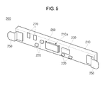
- FIG. 5 is a perspective view of a protection circuit module 200, according to an exemplary embodiment of the present invention, and
- FIG. 6 is a perspective view of the battery pack 10, wherein a case and a label are omitted.
- the battery pack 10 includes a bare cell 100, the protection circuit module 200, a loop antenna 300, the absorber 500, an upper case 910, a lower case 920, and a label 930.
- the absorber 500 is a ferrite sintered body having a high magnetic permeability.
- the absorber 500 is capable of improving the RF sensitivity of the loop antenna 300, leading to improved communication between an external reader and the battery pack 10.
- the bare cell 100 may include: a can 110; an electrode assembly (not shown) disposed in the can; and a cap assembly to seal the can 110.
- the bare cell 100 is a minimum charging/discharging unit of the battery pack 10, and includes a positive electrode and a negative electrode.
- the can 110 may be formed in a generally rectangular parallelepiped shape. An opening may be formed in a surface of the can 110 (e.g., the top surface in FIG. 2 ) other surfaces thereof (e.g., lateral surfaces in FIG. 2 ) may be curved.
- the can 110 may be made of a light-weight metal material such as aluminum (Al), and may serve as a positive terminal.
- the electrode assembly may include a positive electrode plate, a negative electrode plate, and a separator interposed therebetween.
- the electrode assembly may be formed by winding the positive electrode plate, the negative electrode plate, and the separator into a jellyroll-type structure.
- the electrode assembly may be inserted into the can 110, via the opening, which is sealed by the cap assembly.
- the cap assembly includes a cap plate 121, an electrode terminal 122, a gasket 123, an insulating plate (not shown), and a terminal plate (not shown).
- the cap assembly may be combined with the electrode assembly, along with an insulating case (not shown), to seal the opening of the can 110.
- the electrode terminal 122 may serve as a negative terminal.
- the exterior of the bare cell 100 may include a top surface 101 on which the electrode terminal 122 is installed, a opposing bottom surface 102, a pair of large lateral surfaces 103 and 104, and a pair of small lateral surfaces 105 and 106.
- the large lateral surfaces 103 and 104 have a larger surface area than the small lateral surfaces 105 and 106.
- the protection circuit module 200 may be disposed on a surface (e.g., the top surface in FIG. 6 ) of the bare cell 100 and electrically connected to the bare cell 100.
- the protection circuit module 200 may include a protection circuit board 210, a protection circuit device 220, an integrated circuit (IC) chip 230, a charge-discharge terminal 240, a positive electrode lead plate 250, a negative electrode lead plate 260, and a loop antenna terminal 270.
- a positive temperature coefficient (PTC) device (not shown) may be further disposed on the bottom surface of the protection circuit board 210.
- the protection circuit board 210 may be disposed adjacent to a surface of the bare cell 100 (e.g., the top surface in FIG. 6 ) and may be rectangular. Conductive metal patterns (not shown) may be formed in the protection circuit board 210 and may be electrically connected to the protection circuit device 220, the IC chip 230, the charge-discharge terminal 240, the positive electrode lead plate 250, the negative electrode lead plate 260, and the loop antenna terminal 270.
- the protection circuit device 220 may be disposed on the protection circuit board 210.
- the protection circuit device 220 protects the battery pack 10, by monitoring the charge/discharge state of the bare cell 100, and the current, voltage, and temperature of the battery pack 10.
- the IC chip 230 may be disposed on the bottom surface of the protection circuit board 210, and may be electrically connected to the loop antenna 300, via the loop antenna terminal 270.
- the IC chip 230 may perform RF communication with an external electronic apparatus (e.g., a RF signal reader), using the loop antenna 300.
- an external electronic apparatus e.g., a RF signal reader
- the charge-discharge terminal 240 may be disposed on the top surface of the protection circuit board 210.
- the charge-discharge terminal 240 may serve as an electrical connector to supply power to an external electronic apparatus (not shown).
- the positive electrode lead plate 250 may be disposed between the bare cell 100 and the protection circuit board 210, to electrically connect the cap plate 121 and the protection circuit board 210.
- Two positive electrode lead plates 250 may be disposed on opposing sides of the protection circuit board 210.
- the positive electrode lead plates 250 electrically connect the cap plate 121 to the protection circuit board 210.
- one of the positive electrode lead plates 250 may also electrically connect the cap plate 121 to the protection circuit board 210.
- the positive electrode lead plates 250 may be made of nickel or an alloy thereof, for example.
- the negative electrode lead plate 260 may cover a welding through-hole 210a formed in a center portion of the protection circuit board 210.
- the negative electrode lead plate 260 may be electrically connected to the electrode terminal 122, by welding.
- the negative electrode lead plate 260 may be made of nickel or an alloy thereof, for example.
- the loop antenna terminal 270 may be disposed on the bottom surface of the protection circuit board 210.
- the loop antenna terminal 270 may be electrically connected to a connection terminal 330 of the loop antenna 300.
- the loop antenna 300 is shown as being disposed on the large lateral surface 103, but may be disposed on either of the large lateral surfaces 103 and 104.
- the loop antenna 300 may have a shape (e.g., a rectangular shape) corresponding to the large lateral surface 103.
- the loop antenna 300 includes an antenna pattern 310, a coverlay 320, and the connection terminal 330.
- the antenna pattern 310 may be disposed in the coverlay 320, and may be coiled several times along edges of the coverlay 320.
- the antenna pattern 310 may be made of copper, for example.
- the coverlay 320 may be a thin film that covers the antenna pattern 310 and may be made of a polymer resin, e.g., polyimide.
- the connection terminal 330 may be connected to both ends of the antenna pattern 310, so as to be electrically connected to the loop antenna terminal 270.
- the loop antenna 300 receives a RF signal from an external electronic apparatus (e.g., a reader) and transmits the RF signal to the IC chip 230.
- the IC chip 230 may then transmit a response RF signal to the external electronic apparatus, via the loop antenna 300.
- the RF transmission power of the loop antenna 300 may be an electromotive force induced by the RF signal from the external electronic apparatus.
- the loop antenna 300 may transmit and/or receive a 13.56 MHz RF, for example.
- the absorber 500 may be a rectangular plate disposed between the bare cell 100 and the loop antenna 300.
- the absorber 500 can reduce a vortex signal generated by the loop antenna 300 and can increase the density of magnetic flux passing through the loop antenna 300, thereby improving RF sensitivity.
- the absorber 500 may be formed of a ferrite sintered body.
- the absorber 500 may be formed of a sintered body obtained by fully sintering one selected from nickel ferrite, zinc ferrite, nickel-zinc ferrite, and barium ferrite.
- the nickel-zinc ferrite may include from about 47 to about 48 wt% of iron oxide, about 30 wt% of nickel oxide, about 20 wt% of zinc oxide, and from about 2 to about 3 wt% of copper oxide, based on the total weight of the ferrite.
- FIGS. 3 and 4 are respectively 500X and 2000X SEM images of an absorber obtained by sintering a ferrite powder composed of 48 wt% of iron oxide, 30 wt% of nickel oxide, 20 wt% of zinc oxide, and 2 wt% of copper oxide.
- a conventional absorber used in a battery pack or a mobile communication terminal is made of a composite of a ferrite powder and a rubber.
- an absorber includes rubber, the associated material costs and manufacturing processes are increased, as compared with an absorber according to aspects of the present invention.
- the absorber 500 may be manufactured by a simple process of mixing a ferrite powder and a binder, sintering, and removing the binder, which results in reduced manufacturing costs due to the omission of rubber. Moreover, the absorber 500 exhibits a higher magnetic permeability relative to a conventional absorber. Therefore, the absorber 500 has increased RF sensitivity, thereby improving a RF signal recognition distance between the loop antenna 300 and a reader.
- the absorber 500 may have a thickness of about 1 mm, or less, for example, a thickness of from about 0.05 to about 0.3 mm. If the thickness of the absorber 500 is less than about 0.05 mm, the absorber 500 may be easily fractured. On the other hand, if the thickness of the absorber 500 exceeds about 1 mm, the thickness of the battery pack 10 may be unnecessarily increased, thereby decreasing the capacity density of the battery pack 10, with respect to the capacity of the bare cell 100. A polymer layer may be further disposed on the surface of the absorber 500, in order to increase the durability of the ferrite sintered body. The absorber 500 may be attached to the bare cell 100 by a double-sided tape or a liquid adhesive.
- the absorber 500 may cover between from about 50% to about 100% of the large lateral surface 103. If the absorber 500 covers less than about 50% of the large lateral surface 103, the RF sensitivity of the loop antenna 300 may not be significantly enhanced. On the other hand, if the absorber 500 larger than the large lateral surface 103, the capacity density of the battery pack 10, with respect to the capacity of the bare cell 100, may be decreased.
- the absorber 500 may have magnetic permeability of from about 100 to about 115T. Taking into consideration that a mobile terminal uses a small-sized battery, and the absorber 500 has a thickness of less than about 1 mm, the magnetic permeability of the absorber 500 is significantly improved, as compared with a conventional absorber.
- the upper case 910 and the lower case 920 cover the protection circuit module 200 and the bottom surface of the bare cell 100, respectively.
- the label 930 surrounds the large lateral surfaces 103 and 104 and the small lateral surfaces 105 and 106 of the bare cell 100.
- the upper case 910, the lower case 920, and the label 930 protect the bare cell 100, the protection circuit module 200, the absorber 500, and the loop antenna 300 from external impacts.
- the label 930 may be replaced with a hard plastic case. In this case, the absorber 500 and the loop antenna 300 may be formed on an inner surface of the case and coupled to the bare cell 100.
- the battery pack 10 includes the absorber 500 formed of a ferrite sintered body. Therefore, the magnetic permeability thereof is increased, enhancing the RF sensitivity of the loop antenna 300, and resulting in improved communication between an external electronic apparatus and a mobile terminal including the battery pack 10.
- FIG. 7 is an exploded perspective view of a battery pack 10', according to another exemplary embodiment of the present invention.
- the battery pack 10' includes a bare cell 100a and an absorber 600.
- a groove 115 is formed in a large lateral surface 103a of a can 110a of the bare cell 100a.
- the groove 115 is configured to accommodate the absorber 600.
- the absorber 600 may be secured in the groove 115 by a double-sided tape or an adhesive. Since the absorber 600 is received in the groove 115, the overall volume of the battery pack may be reduced, while maintaining the capacity of the bare cell 100a, thereby leading to an increased capacity density of the battery pack.
- the battery pack 10' is substantially the same as the battery pack 10, except for the shape of the bare cell 100a, i.e., except for the bare cell 100a including the groove 115. Therefore, a description of similar elements is omitted.
- FIGS. 8 and 9 are plan views of absorbers 700, 800, according to other exemplary embodiments of the present invention.
- the absorbers 700, 800 can be applied to any of the previously described battery packs.
- the absorbers 700, 800 include ferrite sintered bodies that are divided into individual sections.
- the absorber 700 includes four square-shaped sections 710, 720, 730, and 740, which are arranged such that the absorber 700 corresponds to a large lateral surface of a bare cell.
- the absorber 800 includes four triangle-shaped sections 810, 820, 830, and 840, which are arranged such that the absorber 800 corresponds to a large lateral surface of a bare cell.
- a bare cell gas may be generated in a can, which causes the can to swell.
- an electrode assembly is volumetrically increased, and thus, central portions of the large lateral surfaces of a bare cell protrude outward.
- Such swelling may break a single sheet-type absorber into a plurality of irregular sections.
- the absorbers 700, 800 are formed of ferrite sintered bodies including a plurality of sections, such breakage does not occur.
- an absorber may include a ferrite sintered body that is divided into sections, which are separated by gaps that extend from a central portion of a large lateral surface of a bare cell. Therefore, even when swelling occurs in the bare cell, it is possible to prevent the absorber from being cracked or broken.
- FIG. 10 is a perspective view of a loop antenna 400, according to another exemplary embodiment of the present invention.
- the loop antenna 400 may include an antenna pattern 410, an insulator 420, and a connection terminal 430.
- the loop antenna 400 may be used in place of the loop antenna 300.
- the antenna pattern 410 may be coiled several times into a loop that extends along edges a large lateral surface of a bare cell.
- the antenna pattern 410 may be made of copper.
- the insulator 420 may surround the antenna pattern 410. Thus, the insulator 420 has the same pattern as the antenna pattern 410.
- the connection terminal 430 may be connected to both ends of the antenna pattern 410, and may be electrically connected to a loop antenna terminal (not shown) disposed on a bottom surface of a protection circuit board (not shown).
- the loop antenna 400 has similar RF sensitivity to that of the loop antenna 300 shown in FIGS. 1 through 6 , but is more cost-effective due to the use of the insulator 420. Therefore, it is possible to reduce the manufacturing costs of a battery pack including the loop antenna 400.
- Battery packs according to various exemplary embodiments of the present invention include an absorber formed of a ferrite sintered body, thereby enhancing the RF sensitivity of a loop antenna.
- an absorber formed of a ferrite sintered body thereby enhancing the RF sensitivity of a loop antenna.
- a battery pack that includes an absorber formed of a ferrite sintered body.
- the absorber has increased magnetic permeability, and thus, enhances the RF sensitivity of a loop antenna.
- the absorber does not include rubber, thus simplifying a battery pack manufacturing process and reducing manufacturing costs.
Applications Claiming Priority (1)
| Application Number | Priority Date | Filing Date | Title |
|---|---|---|---|
| KR1020090013488A KR101023884B1 (ko) | 2009-02-18 | 2009-02-18 | 배터리팩 |
Publications (2)
| Publication Number | Publication Date |
|---|---|
| EP2226869A1 true EP2226869A1 (de) | 2010-09-08 |
| EP2226869B1 EP2226869B1 (de) | 2012-12-19 |
Family
ID=42229262
Family Applications (1)
| Application Number | Title | Priority Date | Filing Date |
|---|---|---|---|
| EP10153881A Active EP2226869B1 (de) | 2009-02-18 | 2010-02-17 | Batteriepack und mobiles Kommunikationsendgerät |
Country Status (3)
| Country | Link |
|---|---|
| US (1) | US20100209744A1 (de) |
| EP (1) | EP2226869B1 (de) |
| KR (1) | KR101023884B1 (de) |
Cited By (4)
| Publication number | Priority date | Publication date | Assignee | Title |
|---|---|---|---|---|
| CN103391338A (zh) * | 2012-05-10 | 2013-11-13 | Lg电子株式会社 | 移动终端 |
| EP2782158A1 (de) * | 2013-03-20 | 2014-09-24 | Samsung SDI Co., Ltd. | Batteriepack mit Antenne |
| WO2016032783A1 (en) * | 2014-08-27 | 2016-03-03 | Duracell U.S. Operations, Inc. | Battery pack including an indicator circuit |
| EP2276090B1 (de) * | 2009-07-14 | 2017-10-25 | BlackBerry Limited | Akku mit geringer magnetischer Interferenz und mobile Kommunikationsvorrichtung |
Families Citing this family (24)
| Publication number | Priority date | Publication date | Assignee | Title |
|---|---|---|---|---|
| CN102709494A (zh) * | 2012-01-04 | 2012-10-03 | 瑞声声学科技(深圳)有限公司 | 电池组件 |
| CN102709495B (zh) * | 2012-01-04 | 2015-02-04 | 瑞声声学科技(深圳)有限公司 | 电池组件 |
| KR101320874B1 (ko) * | 2012-05-15 | 2013-10-23 | 주식회사 아모텍 | Nfc 안테나 제조방법 및 이 제조방법으로 제조된 nfc 안테나 |
| US9551758B2 (en) | 2012-12-27 | 2017-01-24 | Duracell U.S. Operations, Inc. | Remote sensing of remaining battery capacity using on-battery circuitry |
| US9083063B2 (en) | 2013-04-03 | 2015-07-14 | The Gillette Company | Electrochemical cell including an integrated circuit |
| KR101339018B1 (ko) * | 2013-04-11 | 2013-12-09 | 에이큐 주식회사 | 엔에프씨 안테나를 구비한 배터리팩 |
| KR101400126B1 (ko) * | 2013-04-11 | 2014-06-27 | 에이큐 주식회사 | Nfc 안테나와 무접점 충전안테나를 구비한 배터리팩 |
| US9478850B2 (en) | 2013-05-23 | 2016-10-25 | Duracell U.S. Operations, Inc. | Omni-directional antenna for a cylindrical body |
| US9726763B2 (en) | 2013-06-21 | 2017-08-08 | Duracell U.S. Operations, Inc. | Systems and methods for remotely determining a battery characteristic |
| KR101469370B1 (ko) * | 2013-06-28 | 2014-12-04 | 주식회사 이그잭스 | 근거리 통신 안테나 모듈 |
| KR200475782Y1 (ko) * | 2013-11-13 | 2015-01-02 | 주식회사 비츠로셀 | 스파이럴 링 타입의 리튬 전지 |
| KR102247011B1 (ko) * | 2014-03-28 | 2021-05-03 | 지이 하이브리드 테크놀로지스, 엘엘씨 | 무선 전력 수신 장치 및 이를 포함하는 이동 통신 단말기 |
| KR102332879B1 (ko) * | 2014-03-28 | 2021-12-01 | 지이 하이브리드 테크놀로지스, 엘엘씨 | 무선 전력 수신 장치 및 이를 포함하는 이동 통신 단말기 |
| KR102483809B1 (ko) * | 2021-04-26 | 2022-12-30 | 지이 하이브리드 테크놀로지스, 엘엘씨 | 무선 전력 수신 장치 및 이를 포함하는 이동 통신 단말기 |
| US9882250B2 (en) | 2014-05-30 | 2018-01-30 | Duracell U.S. Operations, Inc. | Indicator circuit decoupled from a ground plane |
| DE102015202339A1 (de) * | 2015-02-10 | 2016-08-11 | Robert Bosch Gmbh | Batterie mit thermischer Isolierung |
| US10297875B2 (en) | 2015-09-01 | 2019-05-21 | Duracell U.S. Operations, Inc. | Battery including an on-cell indicator |
| US10483634B2 (en) | 2016-11-01 | 2019-11-19 | Duracell U.S. Operations, Inc. | Positive battery terminal antenna ground plane |
| US10151802B2 (en) | 2016-11-01 | 2018-12-11 | Duracell U.S. Operations, Inc. | Reusable battery indicator with electrical lock and key |
| US11024891B2 (en) | 2016-11-01 | 2021-06-01 | Duracell U.S. Operations, Inc. | Reusable battery indicator with lock and key mechanism |
| US10818979B2 (en) | 2016-11-01 | 2020-10-27 | Duracell U.S. Operations, Inc. | Single sided reusable battery indicator |
| US10608293B2 (en) | 2016-11-01 | 2020-03-31 | Duracell U.S. Operations, Inc. | Dual sided reusable battery indicator |
| JP6614401B1 (ja) * | 2018-07-24 | 2019-12-04 | 株式会社村田製作所 | 無線通信デバイス |
| US11837754B2 (en) | 2020-12-30 | 2023-12-05 | Duracell U.S. Operations, Inc. | Magnetic battery cell connection mechanism |
Citations (4)
| Publication number | Priority date | Publication date | Assignee | Title |
|---|---|---|---|---|
| DE2524300A1 (de) * | 1974-06-05 | 1975-12-11 | Tdk Electronics Co Ltd | Mikrowellenabsorber |
| US20030062965A1 (en) * | 2001-09-27 | 2003-04-03 | Stephen Jensen | Circuit board having ferrite containing layer |
| EP1612579A2 (de) * | 2004-07-01 | 2006-01-04 | Omron Corporation | Gerät zur Kommunikation mit RFID-Plaketten mittels einer gesteuerten Richtantenne |
| US20080055046A1 (en) * | 2006-08-31 | 2008-03-06 | Casio Hitachi Mobile Communications Co., Ltd. | Antenna and portable electronic device |
Family Cites Families (13)
| Publication number | Priority date | Publication date | Assignee | Title |
|---|---|---|---|---|
| KR20020090931A (ko) * | 2002-07-23 | 2002-12-05 | (주)에이치엔티 | 알에프아이디 안테나 내장형 배터리팩 |
| KR100517526B1 (ko) * | 2003-04-14 | 2005-09-27 | 주식회사 에이엠아이 씨 | 전자파에 의한 장애 방지를 위한 무선통신 단말기의배터리 모듈 |
| KR200344208Y1 (ko) | 2003-11-26 | 2004-03-10 | 주식회사 웨이브솔루션 | 노이즈 제거용 충전 배터리 |
| JP2005340759A (ja) * | 2004-04-27 | 2005-12-08 | Sony Corp | アンテナモジュール用磁芯部材、アンテナモジュールおよびこれを備えた携帯情報端末 |
| KR100614381B1 (ko) * | 2004-07-29 | 2006-08-21 | 삼성에스디아이 주식회사 | 리튬 이온 이차 전지 |
| EP1724708B1 (de) * | 2005-04-26 | 2016-02-24 | Amotech Co., Ltd. | Magnetisches Blech für RFID-Antenne und ihr Herstellungsverfahren |
| JP4529786B2 (ja) * | 2005-04-28 | 2010-08-25 | 株式会社日立製作所 | 信号処理回路、及びこれを用いた非接触icカード並びにタグ |
| KR100903187B1 (ko) * | 2005-06-25 | 2009-06-17 | 주식회사 엘지화학 | 모바일 디바이스의 정품 전지 인식 시스템 |
| US7562445B2 (en) * | 2005-07-18 | 2009-07-21 | Bartronics America, Inc. | Method of manufacture of an identification wristband construction |
| KR100867405B1 (ko) * | 2007-02-09 | 2008-11-06 | (주)애니쿼터스 | Rfid 리더기의 무선 주파수를 이용한 이동 통신 단말기배터리 충전 장치 |
| CN101683020B (zh) * | 2007-04-11 | 2012-04-18 | 户田工业株式会社 | 电磁波干扰抑制片及其制造方法 |
| KR100864887B1 (ko) * | 2007-05-25 | 2008-10-22 | 삼성에스디아이 주식회사 | 이차 전지 |
| JP4978478B2 (ja) * | 2008-01-11 | 2012-07-18 | ソニー株式会社 | 電磁波抑制放熱シート及び電子機器 |
-
2009
- 2009-02-18 KR KR1020090013488A patent/KR101023884B1/ko active IP Right Grant
-
2010
- 2010-02-16 US US12/706,217 patent/US20100209744A1/en not_active Abandoned
- 2010-02-17 EP EP10153881A patent/EP2226869B1/de active Active
Patent Citations (4)
| Publication number | Priority date | Publication date | Assignee | Title |
|---|---|---|---|---|
| DE2524300A1 (de) * | 1974-06-05 | 1975-12-11 | Tdk Electronics Co Ltd | Mikrowellenabsorber |
| US20030062965A1 (en) * | 2001-09-27 | 2003-04-03 | Stephen Jensen | Circuit board having ferrite containing layer |
| EP1612579A2 (de) * | 2004-07-01 | 2006-01-04 | Omron Corporation | Gerät zur Kommunikation mit RFID-Plaketten mittels einer gesteuerten Richtantenne |
| US20080055046A1 (en) * | 2006-08-31 | 2008-03-06 | Casio Hitachi Mobile Communications Co., Ltd. | Antenna and portable electronic device |
Cited By (11)
| Publication number | Priority date | Publication date | Assignee | Title |
|---|---|---|---|---|
| EP2276090B1 (de) * | 2009-07-14 | 2017-10-25 | BlackBerry Limited | Akku mit geringer magnetischer Interferenz und mobile Kommunikationsvorrichtung |
| CN103391338A (zh) * | 2012-05-10 | 2013-11-13 | Lg电子株式会社 | 移动终端 |
| EP2663056A1 (de) * | 2012-05-10 | 2013-11-13 | LG Electronics, Inc. | Mobiles Endgerät |
| US20130303243A1 (en) * | 2012-05-10 | 2013-11-14 | Sanggil PARK | Mobile terminal |
| US9258393B2 (en) * | 2012-05-10 | 2016-02-09 | Lg Electronics Inc. | Mobile terminal |
| CN103391338B (zh) * | 2012-05-10 | 2016-09-21 | Lg电子株式会社 | 移动终端 |
| EP2782158A1 (de) * | 2013-03-20 | 2014-09-24 | Samsung SDI Co., Ltd. | Batteriepack mit Antenne |
| WO2016032783A1 (en) * | 2014-08-27 | 2016-03-03 | Duracell U.S. Operations, Inc. | Battery pack including an indicator circuit |
| CN106605314A (zh) * | 2014-08-27 | 2017-04-26 | 杜拉塞尔美国经营公司 | 包括指示器电路的电池组 |
| CN106605314B (zh) * | 2014-08-27 | 2019-08-13 | 杜拉塞尔美国经营公司 | 包括指示器电路的电池组 |
| AU2015307027B2 (en) * | 2014-08-27 | 2021-01-07 | Duracell U.S. Operations, Inc. | Battery pack including an indicator circuit |
Also Published As
| Publication number | Publication date |
|---|---|
| KR101023884B1 (ko) | 2011-03-22 |
| KR20100094179A (ko) | 2010-08-26 |
| US20100209744A1 (en) | 2010-08-19 |
| EP2226869B1 (de) | 2012-12-19 |
Similar Documents
| Publication | Publication Date | Title |
|---|---|---|
| EP2226869B1 (de) | Batteriepack und mobiles Kommunikationsendgerät | |
| JP6888053B2 (ja) | グランドプレーンから分離されたインジケータ回路 | |
| US8514135B2 (en) | Protective circuit module and secondary battery pack including the same | |
| EP2200111B1 (de) | Batteriepack | |
| EP2782158A1 (de) | Batteriepack mit Antenne | |
| CN106605314B (zh) | 包括指示器电路的电池组 | |
| EP3240110A1 (de) | Antennenvorrichtung und mobiles endgerät | |
| KR20130054237A (ko) | 안테나 장치, 통신 장치 | |
| WO2005017821A1 (ja) | リーダライタ及び移動体通信装置 | |
| US8771852B2 (en) | Battery pack with contactless power transfer | |
| JP2009104374A (ja) | 機能性icカードおよびそれに用いるラミネート電池 | |
| KR101490513B1 (ko) | 무선충전모듈 | |
| JP2008251283A (ja) | 電子機器及び二次電池 | |
| KR101738132B1 (ko) | 무선충전모듈 | |
| KR101792134B1 (ko) | 무선충전모듈 | |
| KR102325622B1 (ko) | 코일 모듈 및 이를 포함하는 전자 기기 | |
| EP4115488A1 (de) | Empfängerkonstruktion mit hoher intrinsischer qualität |
Legal Events
| Date | Code | Title | Description |
|---|---|---|---|
| PUAI | Public reference made under article 153(3) epc to a published international application that has entered the european phase |
Free format text: ORIGINAL CODE: 0009012 |
|
| 17P | Request for examination filed |
Effective date: 20100217 |
|
| AK | Designated contracting states |
Kind code of ref document: A1 Designated state(s): AT BE BG CH CY CZ DE DK EE ES FI FR GB GR HR HU IE IS IT LI LT LU LV MC MK MT NL NO PL PT RO SE SI SK SM TR |
|
| AX | Request for extension of the european patent |
Extension state: AL BA RS |
|
| RIC1 | Information provided on ipc code assigned before grant |
Ipc: H01M 2/02 20060101AFI20120504BHEP Ipc: H01M 10/04 20060101ALI20120504BHEP |
|
| GRAP | Despatch of communication of intention to grant a patent |
Free format text: ORIGINAL CODE: EPIDOSNIGR1 |
|
| GRAS | Grant fee paid |
Free format text: ORIGINAL CODE: EPIDOSNIGR3 |
|
| GRAA | (expected) grant |
Free format text: ORIGINAL CODE: 0009210 |
|
| AK | Designated contracting states |
Kind code of ref document: B1 Designated state(s): AT BE BG CH CY CZ DE DK EE ES FI FR GB GR HR HU IE IS IT LI LT LU LV MC MK MT NL NO PL PT RO SE SI SK SM TR |
|
| REG | Reference to a national code |
Ref country code: GB Ref legal event code: FG4D |
|
| REG | Reference to a national code |
Ref country code: CH Ref legal event code: EP |
|
| REG | Reference to a national code |
Ref country code: AT Ref legal event code: REF Ref document number: 589793 Country of ref document: AT Kind code of ref document: T Effective date: 20130115 |
|
| REG | Reference to a national code |
Ref country code: DE Ref legal event code: R096 Ref document number: 602010004132 Country of ref document: DE Effective date: 20130221 |
|
| PG25 | Lapsed in a contracting state [announced via postgrant information from national office to epo] |
Ref country code: SE Free format text: LAPSE BECAUSE OF FAILURE TO SUBMIT A TRANSLATION OF THE DESCRIPTION OR TO PAY THE FEE WITHIN THE PRESCRIBED TIME-LIMIT Effective date: 20121219 Ref country code: ES Free format text: LAPSE BECAUSE OF FAILURE TO SUBMIT A TRANSLATION OF THE DESCRIPTION OR TO PAY THE FEE WITHIN THE PRESCRIBED TIME-LIMIT Effective date: 20130330 Ref country code: LT Free format text: LAPSE BECAUSE OF FAILURE TO SUBMIT A TRANSLATION OF THE DESCRIPTION OR TO PAY THE FEE WITHIN THE PRESCRIBED TIME-LIMIT Effective date: 20121219 Ref country code: FI Free format text: LAPSE BECAUSE OF FAILURE TO SUBMIT A TRANSLATION OF THE DESCRIPTION OR TO PAY THE FEE WITHIN THE PRESCRIBED TIME-LIMIT Effective date: 20121219 Ref country code: NO Free format text: LAPSE BECAUSE OF FAILURE TO SUBMIT A TRANSLATION OF THE DESCRIPTION OR TO PAY THE FEE WITHIN THE PRESCRIBED TIME-LIMIT Effective date: 20130319 |
|
| REG | Reference to a national code |
Ref country code: NL Ref legal event code: VDEP Effective date: 20121219 Ref country code: AT Ref legal event code: MK05 Ref document number: 589793 Country of ref document: AT Kind code of ref document: T Effective date: 20121219 |
|
| REG | Reference to a national code |
Ref country code: LT Ref legal event code: MG4D |
|
| PG25 | Lapsed in a contracting state [announced via postgrant information from national office to epo] |
Ref country code: LV Free format text: LAPSE BECAUSE OF FAILURE TO SUBMIT A TRANSLATION OF THE DESCRIPTION OR TO PAY THE FEE WITHIN THE PRESCRIBED TIME-LIMIT Effective date: 20121219 Ref country code: GR Free format text: LAPSE BECAUSE OF FAILURE TO SUBMIT A TRANSLATION OF THE DESCRIPTION OR TO PAY THE FEE WITHIN THE PRESCRIBED TIME-LIMIT Effective date: 20130320 Ref country code: SI Free format text: LAPSE BECAUSE OF FAILURE TO SUBMIT A TRANSLATION OF THE DESCRIPTION OR TO PAY THE FEE WITHIN THE PRESCRIBED TIME-LIMIT Effective date: 20121219 |
|
| PG25 | Lapsed in a contracting state [announced via postgrant information from national office to epo] |
Ref country code: SK Free format text: LAPSE BECAUSE OF FAILURE TO SUBMIT A TRANSLATION OF THE DESCRIPTION OR TO PAY THE FEE WITHIN THE PRESCRIBED TIME-LIMIT Effective date: 20121219 Ref country code: BE Free format text: LAPSE BECAUSE OF FAILURE TO SUBMIT A TRANSLATION OF THE DESCRIPTION OR TO PAY THE FEE WITHIN THE PRESCRIBED TIME-LIMIT Effective date: 20121219 Ref country code: IS Free format text: LAPSE BECAUSE OF FAILURE TO SUBMIT A TRANSLATION OF THE DESCRIPTION OR TO PAY THE FEE WITHIN THE PRESCRIBED TIME-LIMIT Effective date: 20130419 Ref country code: EE Free format text: LAPSE BECAUSE OF FAILURE TO SUBMIT A TRANSLATION OF THE DESCRIPTION OR TO PAY THE FEE WITHIN THE PRESCRIBED TIME-LIMIT Effective date: 20121219 Ref country code: CZ Free format text: LAPSE BECAUSE OF FAILURE TO SUBMIT A TRANSLATION OF THE DESCRIPTION OR TO PAY THE FEE WITHIN THE PRESCRIBED TIME-LIMIT Effective date: 20121219 Ref country code: BG Free format text: LAPSE BECAUSE OF FAILURE TO SUBMIT A TRANSLATION OF THE DESCRIPTION OR TO PAY THE FEE WITHIN THE PRESCRIBED TIME-LIMIT Effective date: 20130319 Ref country code: AT Free format text: LAPSE BECAUSE OF FAILURE TO SUBMIT A TRANSLATION OF THE DESCRIPTION OR TO PAY THE FEE WITHIN THE PRESCRIBED TIME-LIMIT Effective date: 20121219 |
|
| PG25 | Lapsed in a contracting state [announced via postgrant information from national office to epo] |
Ref country code: RO Free format text: LAPSE BECAUSE OF FAILURE TO SUBMIT A TRANSLATION OF THE DESCRIPTION OR TO PAY THE FEE WITHIN THE PRESCRIBED TIME-LIMIT Effective date: 20121219 Ref country code: NL Free format text: LAPSE BECAUSE OF FAILURE TO SUBMIT A TRANSLATION OF THE DESCRIPTION OR TO PAY THE FEE WITHIN THE PRESCRIBED TIME-LIMIT Effective date: 20121219 Ref country code: PL Free format text: LAPSE BECAUSE OF FAILURE TO SUBMIT A TRANSLATION OF THE DESCRIPTION OR TO PAY THE FEE WITHIN THE PRESCRIBED TIME-LIMIT Effective date: 20121219 Ref country code: PT Free format text: LAPSE BECAUSE OF FAILURE TO SUBMIT A TRANSLATION OF THE DESCRIPTION OR TO PAY THE FEE WITHIN THE PRESCRIBED TIME-LIMIT Effective date: 20130419 |
|
| PG25 | Lapsed in a contracting state [announced via postgrant information from national office to epo] |
Ref country code: MC Free format text: LAPSE BECAUSE OF NON-PAYMENT OF DUE FEES Effective date: 20130228 |
|
| PLBE | No opposition filed within time limit |
Free format text: ORIGINAL CODE: 0009261 |
|
| STAA | Information on the status of an ep patent application or granted ep patent |
Free format text: STATUS: NO OPPOSITION FILED WITHIN TIME LIMIT |
|
| PG25 | Lapsed in a contracting state [announced via postgrant information from national office to epo] |
Ref country code: DK Free format text: LAPSE BECAUSE OF FAILURE TO SUBMIT A TRANSLATION OF THE DESCRIPTION OR TO PAY THE FEE WITHIN THE PRESCRIBED TIME-LIMIT Effective date: 20121219 |
|
| 26N | No opposition filed |
Effective date: 20130920 |
|
| PG25 | Lapsed in a contracting state [announced via postgrant information from national office to epo] |
Ref country code: CY Free format text: LAPSE BECAUSE OF FAILURE TO SUBMIT A TRANSLATION OF THE DESCRIPTION OR TO PAY THE FEE WITHIN THE PRESCRIBED TIME-LIMIT Effective date: 20121219 Ref country code: HR Free format text: LAPSE BECAUSE OF FAILURE TO SUBMIT A TRANSLATION OF THE DESCRIPTION OR TO PAY THE FEE WITHIN THE PRESCRIBED TIME-LIMIT Effective date: 20121219 |
|
| REG | Reference to a national code |
Ref country code: IE Ref legal event code: MM4A |
|
| PG25 | Lapsed in a contracting state [announced via postgrant information from national office to epo] |
Ref country code: IT Free format text: LAPSE BECAUSE OF FAILURE TO SUBMIT A TRANSLATION OF THE DESCRIPTION OR TO PAY THE FEE WITHIN THE PRESCRIBED TIME-LIMIT Effective date: 20121219 |
|
| REG | Reference to a national code |
Ref country code: DE Ref legal event code: R097 Ref document number: 602010004132 Country of ref document: DE Effective date: 20130920 |
|
| PG25 | Lapsed in a contracting state [announced via postgrant information from national office to epo] |
Ref country code: IE Free format text: LAPSE BECAUSE OF NON-PAYMENT OF DUE FEES Effective date: 20130217 |
|
| PG25 | Lapsed in a contracting state [announced via postgrant information from national office to epo] |
Ref country code: MT Free format text: LAPSE BECAUSE OF FAILURE TO SUBMIT A TRANSLATION OF THE DESCRIPTION OR TO PAY THE FEE WITHIN THE PRESCRIBED TIME-LIMIT Effective date: 20121219 |
|
| REG | Reference to a national code |
Ref country code: CH Ref legal event code: PL |
|
| PG25 | Lapsed in a contracting state [announced via postgrant information from national office to epo] |
Ref country code: LI Free format text: LAPSE BECAUSE OF NON-PAYMENT OF DUE FEES Effective date: 20140228 Ref country code: CH Free format text: LAPSE BECAUSE OF NON-PAYMENT OF DUE FEES Effective date: 20140228 |
|
| PG25 | Lapsed in a contracting state [announced via postgrant information from national office to epo] |
Ref country code: SM Free format text: LAPSE BECAUSE OF FAILURE TO SUBMIT A TRANSLATION OF THE DESCRIPTION OR TO PAY THE FEE WITHIN THE PRESCRIBED TIME-LIMIT Effective date: 20121219 |
|
| PG25 | Lapsed in a contracting state [announced via postgrant information from national office to epo] |
Ref country code: TR Free format text: LAPSE BECAUSE OF FAILURE TO SUBMIT A TRANSLATION OF THE DESCRIPTION OR TO PAY THE FEE WITHIN THE PRESCRIBED TIME-LIMIT Effective date: 20121219 |
|
| PG25 | Lapsed in a contracting state [announced via postgrant information from national office to epo] |
Ref country code: MK Free format text: LAPSE BECAUSE OF FAILURE TO SUBMIT A TRANSLATION OF THE DESCRIPTION OR TO PAY THE FEE WITHIN THE PRESCRIBED TIME-LIMIT Effective date: 20121219 Ref country code: HU Free format text: LAPSE BECAUSE OF FAILURE TO SUBMIT A TRANSLATION OF THE DESCRIPTION OR TO PAY THE FEE WITHIN THE PRESCRIBED TIME-LIMIT; INVALID AB INITIO Effective date: 20100217 Ref country code: LU Free format text: LAPSE BECAUSE OF NON-PAYMENT OF DUE FEES Effective date: 20130217 |
|
| REG | Reference to a national code |
Ref country code: FR Ref legal event code: PLFP Year of fee payment: 7 |
|
| REG | Reference to a national code |
Ref country code: FR Ref legal event code: PLFP Year of fee payment: 8 |
|
| REG | Reference to a national code |
Ref country code: FR Ref legal event code: PLFP Year of fee payment: 9 |
|
| REG | Reference to a national code |
Ref country code: DE Ref legal event code: R079 Ref document number: 602010004132 Country of ref document: DE Free format text: PREVIOUS MAIN CLASS: H01M0002020000 Ipc: H01M0050100000 |
|
| PGFP | Annual fee paid to national office [announced via postgrant information from national office to epo] |
Ref country code: FR Payment date: 20230208 Year of fee payment: 14 |
|
| P01 | Opt-out of the competence of the unified patent court (upc) registered |
Effective date: 20230528 |
|
| PGFP | Annual fee paid to national office [announced via postgrant information from national office to epo] |
Ref country code: DE Payment date: 20240130 Year of fee payment: 15 Ref country code: GB Payment date: 20240201 Year of fee payment: 15 |