EP2225829B1 - Komparatorschaltung - Google Patents
Komparatorschaltung Download PDFInfo
- Publication number
- EP2225829B1 EP2225829B1 EP08863024A EP08863024A EP2225829B1 EP 2225829 B1 EP2225829 B1 EP 2225829B1 EP 08863024 A EP08863024 A EP 08863024A EP 08863024 A EP08863024 A EP 08863024A EP 2225829 B1 EP2225829 B1 EP 2225829B1
- Authority
- EP
- European Patent Office
- Prior art keywords
- transistors
- terminal
- input
- source
- pmos
- Prior art date
- Legal status (The legal status is an assumption and is not a legal conclusion. Google has not performed a legal analysis and makes no representation as to the accuracy of the status listed.)
- Active
Links
Images


Classifications
-
- H—ELECTRICITY
- H03—ELECTRONIC CIRCUITRY
- H03K—PULSE TECHNIQUE
- H03K5/00—Manipulating of pulses not covered by one of the other main groups of this subclass
- H03K5/22—Circuits having more than one input and one output for comparing pulses or pulse trains with each other according to input signal characteristics, e.g. slope, integral
- H03K5/24—Circuits having more than one input and one output for comparing pulses or pulse trains with each other according to input signal characteristics, e.g. slope, integral the characteristic being amplitude
- H03K5/2472—Circuits having more than one input and one output for comparing pulses or pulse trains with each other according to input signal characteristics, e.g. slope, integral the characteristic being amplitude using field effect transistors
-
- H—ELECTRICITY
- H03—ELECTRONIC CIRCUITRY
- H03F—AMPLIFIERS
- H03F3/00—Amplifiers with only discharge tubes or only semiconductor devices as amplifying elements
- H03F3/45—Differential amplifiers
- H03F3/45071—Differential amplifiers with semiconductor devices only
- H03F3/45076—Differential amplifiers with semiconductor devices only characterised by the way of implementation of the active amplifying circuit in the differential amplifier
- H03F3/45179—Differential amplifiers with semiconductor devices only characterised by the way of implementation of the active amplifying circuit in the differential amplifier using MOSFET transistors as the active amplifying circuit
-
- H—ELECTRICITY
- H03—ELECTRONIC CIRCUITRY
- H03K—PULSE TECHNIQUE
- H03K5/00—Manipulating of pulses not covered by one of the other main groups of this subclass
- H03K5/003—Changing the DC level
-
- H—ELECTRICITY
- H03—ELECTRONIC CIRCUITRY
- H03K—PULSE TECHNIQUE
- H03K5/00—Manipulating of pulses not covered by one of the other main groups of this subclass
- H03K5/22—Circuits having more than one input and one output for comparing pulses or pulse trains with each other according to input signal characteristics, e.g. slope, integral
- H03K5/24—Circuits having more than one input and one output for comparing pulses or pulse trains with each other according to input signal characteristics, e.g. slope, integral the characteristic being amplitude
- H03K5/2436—Circuits having more than one input and one output for comparing pulses or pulse trains with each other according to input signal characteristics, e.g. slope, integral the characteristic being amplitude using a combination of bipolar and field-effect transistors
-
- H—ELECTRICITY
- H03—ELECTRONIC CIRCUITRY
- H03F—AMPLIFIERS
- H03F2200/00—Indexing scheme relating to amplifiers
- H03F2200/411—Indexing scheme relating to amplifiers the output amplifying stage of an amplifier comprising two power stages
-
- H—ELECTRICITY
- H03—ELECTRONIC CIRCUITRY
- H03F—AMPLIFIERS
- H03F2203/00—Indexing scheme relating to amplifiers with only discharge tubes or only semiconductor devices as amplifying elements covered by H03F3/00
- H03F2203/45—Indexing scheme relating to differential amplifiers
- H03F2203/45394—Indexing scheme relating to differential amplifiers the AAC of the dif amp comprising FETs whose sources are not coupled, i.e. the AAC being a pseudo-differential amplifier
-
- H—ELECTRICITY
- H03—ELECTRONIC CIRCUITRY
- H03F—AMPLIFIERS
- H03F2203/00—Indexing scheme relating to amplifiers with only discharge tubes or only semiconductor devices as amplifying elements covered by H03F3/00
- H03F2203/45—Indexing scheme relating to differential amplifiers
- H03F2203/45648—Indexing scheme relating to differential amplifiers the LC comprising two current sources, which are not cascode current sources
-
- H—ELECTRICITY
- H03—ELECTRONIC CIRCUITRY
- H03F—AMPLIFIERS
- H03F2203/00—Indexing scheme relating to amplifiers with only discharge tubes or only semiconductor devices as amplifying elements covered by H03F3/00
- H03F2203/45—Indexing scheme relating to differential amplifiers
- H03F2203/45682—Indexing scheme relating to differential amplifiers the LC comprising one or more op-amps
Definitions
- Comparator switching thresholds of comparators should be long-term stable to achieve a given accuracy.
- the processing of input signals is problematic, which can come close to the negative supply voltage, generally ground.
- no input voltages smaller than the threshold voltage of the NMOS transistors of e.g. 0.7V are recorded, otherwise the N-channel is pinched off.
- the use of a PMOS transistor input pair also allows the recording of low voltage levels down to the negative supply voltage or ground.
- PMOS transistors modem CMOS processes however, have a drift behavior in the threshold voltage during aging due to the thin gate oxide. If these drifts are different in the transistors of the input pair, the comparator may experience an offset during its lifetime. Different temporal courses of the drifts arise through different gate-source voltages, different drain-source voltages or different bulk-source voltages of the PMOS transistors of the input pair. These voltage differences can occur during operation.
- a comparator circuit which has a potential-shifting circuit with a PMOS transistor input pair for receiving the two input signals, the potential of the two input signals or voltage level-shifted as intermediate signals subsequently passes, in particular to a NMOS or npn transistor pair.
- the potential-shifting circuit with the two PMOS input transistors is advantageously drift-compensated by circuitry measures.
- the invention is based on the idea by the use of a PMOS transistor pair as input transistors also low voltage level or up to the negative supply voltage reaching reaching and forward input signals, advantageously by a drift-compensating device occurring at the PMOS input transistors drift through circuit measures are kept the same by the gate-source voltage, the drain-source voltage and the bulk-source voltage of both PMOS input transistors is kept the same.
- the intermediate signals are subsequently passed on to an NMOS transistor input pair (or else NPN transistor input pair) without such a drift behavior, which due to the potential shift can pick up all the shifted input signals output by the PMOS input transistor pair, so that also low Input signals can be recorded.
- the two PMOS input transistors are advantageously connected in such a way that the relevant voltages present at their terminals, ie gate-source voltages, drain-source voltages and bulk-source voltages, are always identical to one another by circuitry measures and are kept almost constant ,
- the changes occurring during aging of the threshold voltage (drift) of the two PMOS input transistors have due to the circuitry Measures advantageously the same time course, so that they rest as a common-mode signal to the subsequent sequence comparator and thus remain ineffective due to its common mode rejection.
- the sequence comparator has an NMOS input pair, no relevant drift behavior occurs in it.
- current sources are advantageously provided, which are constructed with current mirrors made of PNP bipolar transistors or with cascoded current mirrors of PMOS transistors. In the latter case, the effect of the PMOS drift in the current mirrors remains ineffective, since the gate-source voltage, the drain-source voltage and the bulk-source voltage of the PMOS transistors of the current mirror are kept equal.
- the changes in the threshold voltages (drift) of these transistors thus have the same time course and do not affect the accuracy of the current mirror and thus the overall circuit.
- a comparator circuit can thus be formed which, compared to conventional comparators, has only small additional circuit measures and can be designed to save space and with low energy consumption as an integrated circuit.
- input signals can be recorded at voltage levels which are close to the negative supply voltage. According to the invention, no or no relevant impairment of the switching characteristics (in particular of the offset) of the entire comparator circuit takes place despite the drift behavior of the transistors used.
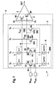
- a comparator circuit 1 has according to Fig. 1 a sequence comparator 2 with a plus input 2a and a minus input 2b on.
- the sequence comparator 2 is constructed, for example, in a manner known per se and has an NMOS transistor or n-channel MOSFET N3 and a further NMOS transistor N4 in its input stage 9, which is generally designed as a differential amplifier, at its two inputs 2a, 2b ,
- the output OUT of the sequence comparator 2 forms the output of the entire comparator circuit 1.
- the NMOS transistors N3 and N4 and NPN transistors may be provided.
- an input circuit 3 is set before the sequence comparator 2.
- the input circuit 3 with the MOSFETs N3 and N4 having input stage 9 of the sequence comparator 2 form an input stage circuit 8 of the entire inventive comparator circuit first
- the input circuit 3 has two PMOS input transistors P1 and P2 (p-channel MOSFETs). To the gate G1 of the first PMOS input transistor P1, the positive input IN POS is set. Accordingly, the negative input IN- NEG is applied to the gate G2 of the second PMOS input transistor P2.
- the Bulkan Bach B1 and B2 are applied to the respective sources S1 and S2 of the PMOS input transistors P1, P2.
- the source terminal S1 is connected via a first DC power source 4 to the positive supply voltage Uv. Accordingly, the source S2 via a second DC power source 5 is applied to the supply voltage Uv. Accordingly, the drain terminal D1 of the first PMOS input transistor P1 is connected via a third DC power source 6 and the drain terminal D2 of the second PMOS transistor P2 via a fourth DC power source 7 to ground GND.
- the source terminal S1 is placed on the plus input 2a of the sequence comparator 2. Accordingly, the source terminal S2 is placed on the negative input 2b of the sequence comparator 2.
- An NMOS transistor N1 is connected with its gate GN1 to the source terminal S1, with its drain terminal DN1 to the supply voltage Uv and with its source terminal SN1 to the drain terminal D1 of the PMOS input transistor P1. Accordingly, the gate terminal GN2 of a second NMOS transistor N2 is connected to the source terminal S2 of the PMOS input transistor P2, its drain terminal DN2 is connected to the supply voltage Uv, and its source terminal SN2 is connected to the drain terminal D2 of the PMOS Input transistor P2 placed.
- Fig. 2a and Fig. 2b show alternative embodiments of the subcircuits II and III, ie, the DC power sources 4 to 7 from Fig. 1 ,
- Fig. 2a shows by way of example with the NPN bipolar transistors QN1 to QN4 and the PNP bipolar transistors QP1 to QP3 two simple current mirror, in the event that bipolar transistors are available in the technology used, such as the z. B. in a BiCMOS process is the case.
- the BiCMOS process allows PNP and NPN bipolar transistors to be formed in a mixing process.
- QN2 to QN4 are mirror transistors to the reference transistor QN1.
- the transistors QP2 and QP3 are mirror transistors to the reference transistor QP1.
- the reference current or collector current I IREF flows through the reference transistor QN1.
- QN1 and QN2 Due to the same nature of QN1 and QN2 and The same base-emitter voltage of QN1 and QN2 also flows through QN2 collector current I. Also, the base-emitter voltage of QN3 and QN4 is equal to that of QN1. However, the transistors QN3 and QN4 each consist of n + 1 single cells or individual transistors, as indicated by the indication "cell, cells", so that through them a total of the current (n + 1) ⁇ I flows. QN3 and QN4 constitute the DC power sources 6 and 7.
- the collector current of QP1 is equal to that of QN2, so that the collector current I flows through the reference transistor QP1.
- the base-emitter voltage of QP2 and QP3 is equal to that of QP1.
- the transistors QP2 and QP3 each consist of n single cells or individual transistors, so that through them a total of the current n ⁇ I flows.
- QP2 and QP3 constitute the DC power sources 4 and 5.
- Fig. 2b shows by way of example with the n-channel MOSFETs MN1 to MN5 and the p-channel MOSFETs MP1 to MP7 two current mirror in the event that no bipolar transistors are available in the technology used, as is the case for example in a pure CMOS process is.
- the PMOS current mirrors are cascoded in a known form.
- MN2 to MN5 are mirror transistors to the reference transistor MN1.
- the transistors MP4 and MP6 are mirror transistors to the reference transistor MP2.
- the transistor MP1 provides a reference voltage for the cascode transistors MP3, MP5 and MP7.
- Wp and Wn here describe the channel width, Lp and Ln the channel length, so that Wp / Lp and Wn / Ln represent the corresponding ratios that are relevant here as parameters of the transistors.
- the reference current or drain current I IREF flows through the reference transistor MN1. Due to the same nature of MN1, MN2 and MN3 and the same gate-source voltage of MN1, MN2 and MN3 flows through MN2 and MN3, the drain current I.
- the gate-source voltage of MN4 and MN5 corresponds to that of MN1.
- the width of the transistors MN4 and However, MN5 is greater by a factor of n + 1, so that in total the current (n + 1) ⁇ I flows through them.
- MN4 and MN5 constitute the DC power sources 6 and 7.
- the drain current of MP2 is equal to that of MN3, so that the drain current I flows through the reference transistor MP2.
- the gate-to-source voltage of MP4 and MP6 is the same as that of MP2.
- the width of the transistors MP4 and MP6 is larger by a factor n, so that in total the current n ⁇ I flows through them.
- MP4 and MP6 form the DC sources 4 and 5.
- the drain-to-source voltages of MP2, MP4 and MP4 will be kept the same. This is done by the cascode transistors MP3, MP5 and MP7, whose gate potential is formed by the transistor MP1, by the same drain current flowing through it, which also flows through MN2.
- MP1 has a width that is smaller by a factor of 1/4, so that its gate-source voltage is about 200 mV larger than that of the cascode transistors MP3, MP5 and MP7. This ensures that the mirror transistors always operate in saturation.
- the circuit consisting of MN1 to MN5 and MP1 to MP7, is basically known. It is relevant that the PMOS drift can have no influence on their current mirror behavior since the reference transistor MP2 and the mirror transistors MP4 and MP6 always have the same gate-source voltage, the same drain-source voltage and the same bulk-source voltage exhibit. Thus, the currents through the transistors P1 and P2, and N1 and N2 of the input circuit 3 of the Fig. 1 flow, always equal to each other.
- the PMOS input transistors P1 and P2 can process input signals In POS and In NEG , which can approach the negative supply voltage GND.
- U BS ⁇ 1 U BS ⁇ 2 ⁇ constant .
- P1 and P2 serve as drift-compensated level shifters or voltage level-shifting (potential-shifting) means for the subsequent sequence comparator 2.
- the gate-source voltages UGS1 and UGS2 of the PMOS input transistors P1 and P2 are the same because the same current n * I flows through them and because their drain-source voltages UDS1 and UDS2 are the same.
- the drain-source voltages of the PMOS input transistors P1 and P2 are the same because they are given by the gate-source voltages UGSN1 and UGSN2 of the two NMOS transistors N1 and N2, which are also traversed by the same currents I, and which therefore have the same gate-source voltage UGSN1 and UGSN2.
- the bulk-source voltages UBS1 and UBS2 of the PMOS input transistors P1 and P2 are equal (and equal to zero) because the source terminals S1 and S2, respectively, of each PMOS transistor are connected to its bulk terminals B1 and B2, respectively.
- N1 and N2 serve to clamp the drain-to-source voltages U DS1 and U DS2 of the PMOS input transistors P1 and P2, respectively to fix them by their gate-source voltages U GSN1 and U GSN2 ;
- N1 and N2 serve as voltage adjusting devices.
- the threshold voltage in the PMOS input transistors P1 and P2 alters during the lifetime of the entire integrated comparator circuit 1 equally, since the gate-source voltages, drain-source voltages and bulk-source voltages are equal to each other and kept constant.
- NMOS transistors or NPN transistors have a non-relevant drift behavior.
- the NMOS transistor input pair (consisting of N3 and N4) or a corresponding NPN transistor pair of the sequence comparator 2 therefore causes no relevant offset during the lifetime.
- PMOS current mirrors and PMOS current sources with cascode transistors are correspondingly Fig. 2a respectively.
- Fig. 2b intended.
- the entire comparator circuit 1 is advantageously designed as an integrated circuit.
Landscapes
- Physics & Mathematics (AREA)
- Nonlinear Science (AREA)
- Engineering & Computer Science (AREA)
- Power Engineering (AREA)
- Measurement Of Current Or Voltage (AREA)
- Manipulation Of Pulses (AREA)
Description
- Komparatorschaltschwellen von Komparatoren sollten zur Erzielung einer vorgegebenen Genauigkeit langzeitstabil sein. Hierbei ist insbesondere die Verarbeitung von Eingangssignalen problematisch, die an die negative Versorgungsspannung, im Allgemeinen Masse, heranreichen können. Werden diese Eingangssignale auf die Gates eines NMOS-Transistor-Paares gegeben, können in der Regel keine Eingangsspannungen die kleiner als die Einsatzspannung (bzw. Schwellspannung oder threshold voltage) der NMOS-Transistoren von z.B. 0.7V sind, aufgenommen werden, da sonst der N-Kanal abgeschnürt wird. Der Einsatz eines PMOS-Transistor- Eingangspaars ermöglicht auch die Aufnahme niedriger Spannungspegel bis herab zur negativen Versorgungsspannung bzw. Masse. PMOS-Transistoren modemer CMOS-Prozesse weisen jedoch aufgrund des dünnen Gate-Oxids ein Driftverhalten in der Einsatzspannung (threshold voltage) während der Alterung auf. Sind diese Driften bei den Transistoren des Eingangspaars verschieden, kann beim Komparator während seiner Lebensdauer ein Offset entstehen. Unterschiedliche zeitliche Verläufe der Driften entstehen durch unterschiedliche Gate-Source-Spannungen, unterschiedliche Drain-Source-Spannungen oder unterschiedliche Bulk-Source-Spannungen der PMOS-Transistoren des Eingangspaars. Diese Spannungsunterschiede können während des Betriebes auftreten.
- Die wissenschaftliche Publikation 'CARRILLO J M ET AL: "Constant-gm Constant-Slew-Rate High-Bandwidth Low-Voltage Rail-to-Rail CMOS Input Stage for VLSI Cell Libraries", IEEE Journal of Solid-State Circuits, Bd. 38, Nr. 8, 1; August 2003, Seiten 1364-1372' offenbart eine Rail-to-Rail Diferenzeingangsstufe umfassend eine potentialverschiebende Schaltung.
- Erfindungsgemäß wird eine Komparatorschaltung gemäß Anspruch 1 geschaffen, die eine potentialverschiebende Schaltung mit einem PMOS-Transistor- Eingangspaar zur Aufnahme der beiden Eingangssignale aufweist, die die beiden Eingangssignale potentialverschoben bzw. Spannungspegel-verschoben als Zwischensignale nachfolgend weitergibt, insbesondere auf ein NMOS- bzw. npn-Transistor-Paar. Die potentialverschiebende Schaltung mit den beiden PMOS- Eingangstransistoren ist vorteilhafterweise durch schaltungstechnische Maßnahmen driftkompensiert.
- Der Erfindung liegt der Gedanke zugrunde, durch den Einsatz eines PMOS-Transistor-Paares als Eingangstransistoren auch niedrige Spannungspegel bzw. bis an die negative Versorgungsspannung heran reichende Eingangssignale aufzunehmen und weiterzugeben, wobei vorteilhafterweise durch eine driftkompensierende Einrichtung die bei den PMOS- Eingangstransistoren auftretenden Driften durch schaltungstechnische Maßnahmen gleich gehalten werden, indem die Gate-Source-Spannung, die Drain-Source-Spannung und die Bulk-Source-Spannung beider PMOS- Eingangstransistoren gleich gehalten wird. Vorteilhafterweise werden die Zwischensignale nachfolgend an ein NMOS-Transistor-Eingangspaar (oder auch NPN-Transistor-Eingangpaar) ohne ein derartiges Driftverhalten weitergegeben, das aufgrund der Potentialverschiebung sämtliche von dem PMOS- Eingangstransistor-Paar ausgegebenen, verschobenen Eingangssignale aufnehmen kann, so dass auch niedrige Eingangsignale aufgenommen werden können.
- Die beiden PMOS- Eingangstransistoren werden vorteilhafterweise derartig geschaltet, dass die an ihren Anschlüssen anliegenden relevanten Spannungen, d.h. Gate-Source-Spannungen, Drain-Source-Spannungen und Bulk-Source-Spannungen, durch schaltungstechnische Maßnahmen untereinander stets gleich sind und nahezu konstant gehalten werden. Die während der Alterung auftretenden Änderungen der Einsatzspannung (Drift) der beiden PMOS-Eingangstransistoren haben aufgrund der schaltungstechnischen Maßnahmen vorteilhafterweise den gleichen zeitlichen Verlauf, so dass sie als Gleichtaktsignal an dem nachfolgenden Folge-Komparator anliegen und damit aufgrund dessen Gleichtaktunterdrückung wirkungslos bleiben.
- Indem der Folge-Komparator ein NMOS-Eingangspaar hat, tritt bei ihm kein relevantes Driftverhalten auf. In der potentialverschiebenden Schaltung sind zusätzlich zu den beiden PMOS-Eingangstransistoren vorteilhafterweise Stromquellen vorgesehen, die mit Stromspiegeln aus PNP- Bipolartransistoren oder mit kaskodierten Stromspiegeln aus PMOS-Transistoren aufgebaut sind. Im letzteren Fall bleibt die Auswirkung der PMOS-Drift in den Stromspiegeln wirkungslos, da die Gate-Source-Spannung, die Drain-Source-Spannung und die Bulk-Source-Spannung der PMOS-Transistoren der Stromspiegel gleich gehalten werden. Die Änderungen der Einsatzspannungen (Drift) dieser Transistoren haben somit den gleichen zeitlichen Verlauf und beeinflussen die Genauigkeit der Stromspiegel und damit der Gesamtschaltung nicht.
- Erfindungsgemäß kann somit eine Komparatorschaltung ausgebildet werden, die gegenüber herkömmlichen Komparatoren nur geringe zusätzliche Schaltungsmaßnahmen aufweist und als integrierte Schaltung platzsparend und mit niedrigem Energieverbrauch ausgebildet werden kann. Erfindungsgemäß können Eingangssignale mit Spannungspegeln aufgenommen werden, die nahe an die negative Versorgungsspannung heranreichen, wobei erfindungsgemäß trotz des auftretenden Driftverhaltens der eingesetzten Transistoren kein bzw. keine relevante Beeinträchtigung der Schalteigenschaften (insbesondere des Offsets) der gesamten Komparatorschaltung stattfindet.
-
- Fig. 1
- zeigt ein Schaltbild einer erfindungsgemäßen Komparatorschaltung gemäß einer Ausführungsform;
- Fig. 2a
- eine Ausführung der Teilschaltungen II und III gemäß einer Ausführungsform in BiCMOS;
- Fig. 2b
- eine Ausführung der Teilschaltung der Teilschaltung II und III gemäß einer zu
Fig. 2a alternativen Ausführungsform in CMOS. - Eine Komparatorschaltung 1 weist gemäß
Fig. 1 einen Folge-Komparator 2 mit einem Plus-Eingang 2a und einem Minus-Eingang 2b auf. Der Folge-Komparator 2 ist z.B. in an sich bekannter Weise aufgebaut und weist in seiner im Allgemeinen als Differenzverstärker ausgebildeten Eingangsstufe 9 an seinen beiden Eingängen 2a, 2b einen NMOS-Transistor bzw. n-Kanal MOSFET N3 und einen weiteren NMOS-Transistor N4 auf. Der Ausgang OUT des Folge-Komparators 2 bildet den Ausgang der gesamten Komparatorschaltung 1. Anstelle der NMOS-Transistoren N3 und N4 können auch NPN-Transistoren vorgesehen sein. - Erfindungsgemäß ist vor den Folge-Komparator 2 eine Eingangsschaltung 3 gesetzt. Somit bilden die Eingangsschaltung 3 mit der die MOSFETs N3 und N4 aufweisenden Eingangsstufe 9 des Folge-Komparators 2 eine Eingangsstufenschaltung 8 der gesamten erfindungsgemäßen Komparatorschaltung 1.
- Die Eingangsschaltung 3 weist zwei PMOS-Eingangstransistoren P1 und P2 (p-Kanal MOSFETs) auf. An das Gate G1 des ersten PMOS- Eingangstransistors P1 ist der positive Eingang INPOS gelegt. Entsprechend ist an das Gate G2 des zweiten PMOS-Eingangstransistors P2 der negative Eingang IN-NEG gelegt. Die Bulkanschlüsse B1 und B2 sind an die jeweiligen Sourceanschlüsse S1 und S2 der PMOS-Eingangstransistoren P1, P2 gelegt. Der Sourceanschluss S1 ist über eine erste Gleichstromquelle 4 an die positive Versorgungsspannung Uv gelegt. Entsprechend ist die Source S2 über eine zweite Gleichstromquelle 5 an die Versorgungsspannung Uv gelegt. Entsprechend ist der Drain-Anschluss D1 des ersten PMOS-Eingangstransistors P1 über eine dritte Gleichstromquelle 6 und der Drain-Anschluss D2 des zweiten PMOS-Transistors P2 über eine vierte Gleichstromquelle 7 auf Masse GND gelegt.
- Der Source-Anschluss S1 ist auf den Plus-Eingang 2a des Folge- Komparators 2 gelegt. Entsprechend ist der Source-Anschluss S2 auf den Minus-Eingang 2b des Folge-Komparators 2 gelegt.
- Ein NMOS-Transistor N1 ist mit seinem Gate GN1 an den Source-Anschluss S1, mit seinem Drain-Anschluss DN1 an die Versorgungsspannung Uv und mit seinem Source-Anschluss SN1 an den Drain-Anschluss D1 des PMOS-Eingangstransistors P1 gelegt. Entsprechend ist der Gate-Anschluss GN2 eines zweiten NMOS-Transistors N2 an den Source-Anschluss S2 des PMOS-Eingangstransistors P2 gelegt, sein Drain-Anschluss DN2 ist an die Versorgungsspannung Uv und sein Source-Anschluss SN2 an den Drain-Anschluss D2 des PMOS-Eingangstransistors P2 gelegt.
-
Fig. 2a undFig. 2b zeigen alternative Ausführungsformen der Teilschaltungen II und III, d.h. der Gleichstromquellen 4 bis 7 ausFig. 1 . -
Fig. 2a zeigt beispielhaft mit den NPN-Bipolartransistoren QN1 bis QN4 und den PNP-Bipolartransistoren QP1 bis QP3 zwei einfache Stromspiegel, für den Fall, dass in der verwendeten Technologie Bipolartransistoren zur Verfügung stehen, wie das z. B. in einem BiCMOS-Prozess der Fall ist. Durch den BiCMOS-Prozess können PNP- und NPN-Bipolartransistoren in einem Mischprozess ausgebildet werden. In der Schaltung derFig. 2a sind QN2 bis QN4 Spiegeltransistoren zu dem Referenztransistor QN1. Die Transistoren QP2 und QP3 sind Spiegeltransistoren zu dem Referenztransistor QP1. Durch den Referenztransistor QN1 fließt der Referenzstrom bzw. Kollektorstrom I = IREF. Aufgrund der gleichen Beschaffenheit von QN1 und QN2 und der gleichen Basis-Emitter-Spannung von QN1 und QN2 fließt auch durch QN2 der Kollektorstrom I. Auch die Basis-Emitter-Spannung von QN3 und QN4 entspricht der von QN1. Die Transistoren QN3 und QN4 bestehen jedoch aus jeweils n+1 Einzelzellen bzw. Einzeltransistoren, wie durch die Angabe "cell, cells" verdeutlicht, so dass durch sie insgesamt jeweils der Strom (n+1)·I fließt. QN3 und QN4 bilden die Gleichstromquellen 6 und 7. - Der Kollektorstrom von QP1 ist gleich dem von QN2, so dass durch den Referenztransistor QP1 der Kollektorstrom I fließt. Die Basis-Emitter-Spannung von QP2 und QP3 entspricht derjenigen von QP1. Die Transistoren QP2 und QP3 bestehen jedoch aus jeweils n Einzelzellen bzw. Einzeltransistoren, so dass durch sie insgesamt jeweils der Strom n·I fließt. QP2 und QP3 bilden die Gleichstromquellen 4 und 5.
-
Fig. 2b zeigt beispielhaft mit den n-Kanal-MOSFETs MN1 bis MN5 und den p-Kanal-MOSFETs MP1 bis MP7 zwei Stromspiegel für den Fall, dass in der verwendeten Technologie keine Bipolartransistoren zur Verfügung stehen, wie das z.B. in einem reinen CMOS-Prozeß der Fall ist. Die PMOS- Stromspiegel sind in bekannter Form kaskodiert ausgeführt. In der Schaltung derFig. 2b sind MN2 bis MN5 Spiegeltransistoren zu dem Referenztransistor MN1. Die Transistoren MP4 und MP6 sind Spiegeltransistoren zu dem Referenztransistor MP2. Der Transistor MP1 stellt eine Referenzspannung für die Kaskodetransistoren MP3, MP5 und MP7 zur Verfügung. Wp und Wn beschreiben hierbei die Kanalbreite, Lp und Ln die Kanallänge, sodass Wp/Lp und Wn/Ln die entsprechenden Verhältnisse wiedergeben, die als Kenngrößen der Transistoren hier relevant sind. - Durch den Referenztransistor MN1 fließt der Referenzstrom bzw. Drainstrom I = IREF. Aufgrund der gleichen Beschaffenheit von MN1, MN2 und MN3 und dergleichen Gate-Source-Spannung von MN1, MN2 und MN3 fließt auch durch MN2 bzw. MN3 der Drainstrom I. Auch die Gate-Source-Spannung von MN4 und MN5 entspricht der von MN1. Die Weite der Transistoren MN4 und MN5 ist jedoch jeweils um den Faktor n+1 größer, so dass durch sie insgesamt jeweils der Strom (n+1)·I fließt. MN4 und MN5 bilden die Gleichstromquellen 6 und 7.
- Der Drainstrom von MP2 ist gleich dem von MN3, so dass durch den Referenztransistor MP2 der Drainstrom I fließt. Die Gate-Source-Spannung von MP4 und MP6 entspricht der der von MP2. Die Weite der Transistoren MP4 und MP6 ist jedoch jeweils um den Faktor n größer, so dass durch sie insgesamt jeweils der Strom n·I fließt. MP4 und MP6 bilden die Gleichstromquellen 4 und 5. Damit die Auswirkung der PMOS-Drift ohne Wirkung auf das Verhalten des PMOS-Stromspiegels bleibt, werden die Drain-Source-Spannungen von MP2, MP4 und MP4 gleich gehalten werden. Hierzu dienen die Kaskodetransistoren MP3, MP5 und MP7, deren Gate-Potential von dem Transistor MP1 gebildet wird, indem durch ihn der gleiche Drainstrom fließt, der auch durch MN2 fließt. Gegenüber MP2 hat MP1 jedoch eine um den Faktor 1/4 kleinere Weite, so dass seine Gate-Source-Spannung etwa 200mV größer ist als die der Kaskodetransistoren MP3, MP5 und MP7. Das stellt sicher, dass die Spiegeltransistoren stets in Sättigung arbeiten.
- Die Schaltung, bestehend aus MN1 bis MN5 und MP1 bis MP7, ist grundsätzlich bekannt. Relevant ist, dass die PMOS-Drift keinen Einfluß auf deren Stromspiegelverhalten haben kann, da der Referenztransistor MP2 und die Spiegeltransistoren MP4 und MP6 stets die gleiche Gate-Source-Spannung, die gleiche Drain-Source-Spannung und die gleiche Bulk-Source-Spannung aufweisen. Somit sind auch die Ströme, die durch die Transistoren P1 und P2, bzw. N1 und N2 der Eingangsschaltung 3 der
Fig. 1 fließen, untereinander stets gleich. - Die PMOS- Eingangstransistoren P1 und P2 können Eingangssignale InPOS und InNEG verarbeiten, die an die negative Versorgungsspannung GND heranreichen können. Durch die beiden NMOS-Transistoren N1 und N2 sowie die zusätzlichen Stromquellen 4, 5, 6, 7 werden schaltungstechnische Maßnahmen getroffen, durch die die PMOS-Drift keinen Einfluss auf die gesamte Komparatorschaltung 1 hat. Die Gate-Source-Spannungen UGS1 und UGS2 sind hierdurch stets gleich und werden konstant gehalten. Entsprechend werden auch die Drain-Source-Spannungen UOS1 und UDS2 stets gleich und im Wesentlichen konstant gehalten, und es werden auch die Bulk-Source-Spannungen UBS1 und UBS2 gleich und im Wesentlichen konstant gehalten, d.h.

so dass P1 und P2 als driftkompensierte Level-Shifter bzw. Spannungspegelverschiebende (potentialverschiebende) Mittel für den nachfolgenden Folge-Komparator 2 dienen. - Die Gate-Source-Spannungen UGS1 und UGS2 der PMOS- Eingangstransistoren P1 und P2 sind gleich, weil durch sie jeweils der gleiche Strom n·I hindurchfließt und weil ihre Drain-Source-Spannungen UDS1 und UDS2 gleich sind. Die Drain-Source-Spannungen der PMOS-Eingangstransistoren P1 und P2 sind gleich, weil sie durch die Gate-Source-Spannungen UGSN1 und UGSN2 von den beiden NMOS-Transistoren N1 und N2 vorgegeben werden, die ebenfalls von gleichen Strömen I durchflossen werden, und die deshalb die gleiche Gate-Source-Spannung UGSN1 und UGSN2 aufweisen. Die Bulk-Source-Spannungen UBS1 und UBS2 der PMOS- Eingangstransistoren P1 und P2 sind gleich (und gleich Null), weil jeweils der Source-Anschluss S1 bzw. S2 eines jeden PMOS-Transistors mit seinem BulkAnschluss B1 bzw. B2 verbunden ist.
- An den baugleichen PMOS-Eingangstransistoren P1 und P2 fällt jeweils die gleiche aussteuernde Gate-Source-Spannung UGS1 = UGS2 ab, so dass die PMOS-Eingangstransistoren P1 und P2 Zwischensignale Zpos und Zneg ausgeben, für die etwa gilt: Zpos - INPOS = Zneg - INNEG = UGS1 = UGS2.
- N1 und N2 dienen dazu, die Drain-Source-Spannungen UDS1 und UDS2 der PMOS-Eingangstransistoren P1 und P2 aufzuspannen bzw. durch ihre Gate-Source-Spannungen UGSN1 und UGSN2 festzulegen; somit dienen N1 und N2 erfindungsgemäß als spannungseinstellende Einrichtungen.
- Dies wird aus dem nachfolgenden Beispiel ersichtlich, bei dem die Einsatzspannung der PMOS-Transistoren P1 und P2 UTh1 = UTh2 = 0,5V und die der NMOS-Transistoren N1 und N2 UThn1 = UThn2 = 0,5V sei. Die effektive Gate-Source-Spannung (bzw. gate source overdrive voltage) von P1 und P2 sei durch entsprechende Dimensionierung von Länge und Weite UGS.eff = 0,4V, woraus sich insgesamt eine Gate-Source-Spannung für P1 und P2 von UGS1 = UTh1 + UGS1.eff = 0,9V bzw. UGS2 = UTh2 + UGS2.eff = 0,9V ergibt. Die effektive Gate-Source-Spannung (bzw. gate source overdrive voltage) von N1 und N2 sei durch entsprechende Dimensionierung von Länge und Weite UGSN.eff = 0,2V, woraus sich insgesamt eine Gate-Source-Spannung für N1 und N2 von UGSN1 = UThn1 + UGSN1.eff = 0,7V bzw. UGSN2 = UThn2 + UGSN2.eff = 0,7V ergibt. Falls z.B. INPOS=1V und INNEG = 0V, so stellen sich aufgrund der Gate-Source-Spannungen UGS1 = UGS2 = 0,9V Potentiale US1 = UGN1 = Zpos = 1,9V und US2 = UGN2 = Zneg = 0,9V ein. An den NMOS-Transistoren N1 und N2 fällt jeweils UGSN1 = UGSN2 = 0,7V ab, wobei die Gate-Source-Spannung der NMOS- Transistoren N1 und N2 geringer als die der PMOS-Transistoren sein muss, damit die Stromquellen 6 und 7 nicht abgeschnürt werden. Da die Source-Anschlüsse SN1 und SN2 an den Drain-Anschlüssen D1 und D2 liegen, wird somit die Drain-Source-Spannung der PMOS- Eingangstransistoren P1 und P2 festgelegt. Durch N1 und N2 fließt weiterhin ein zusätzlicher Strom I, so dass durch die Gleichstromquellen 6 und 7 der Gesamtstrom (n+1)I bzw. etwa (n+1)I' fließt. Der Faktor n kann z.B. auf n=4 festgelegt werden.
- Die Einsatzspannung in der PMOS-Eingangstransistoren P1 und P2 verändert sich während der Lebensdauer der gesamten integrierten Komparatorschaltung 1 gleichermaßen, da die Gate-Source-Spannungen, Drain-Source-Spannungen und Bulk-Source-Spannungen untereinander gleich sind und konstant gehalten werden. Die unvermeidbaren Änderungen der Einsatzspannungen UTh1 und UTh2 von P1 und P2 rufen eine Verschiebung der Pegel an den Eingängen 2a, 2b des Folge-Komparators 2 hervor. Aufgrund der erfindungsgemäßen schaltungstechnischen Maßnahmen haben UTh1 und UTh2 den gleichen zeitlichen Verlauf:

- Die Änderung ΔUTh1 = ΔUTh2 liegen als Gleichtaktsignal am Folge- Komparator 2 an und bleiben somit aufgrund der Gleichtaktunterdrückung wirkungslos.
- NMOS-Transistoren oder auch NPN-Transistoren weisen ein nicht relevantes Driftverhalten auf. Das NMOS-Transistor-Eingangspaar (bestehend aus N3 und N4) oder ein entsprechendes NPN-Transistor-Paar des Folge- Komparators 2 verursacht während der Lebensdauer daher keinen relevanten Offset.
- Vorteilhafterweise sind in dem Folge-Komparator 2 PMOS-Stromspiegel und PMOS-Stromquellen mit Kaskodetransistoren entsprechend
Fig. 2a bzw.Fig. 2b vorgesehen. - Die gesamte Komparatorschaltung 1 ist vorteilhafterweise als integrierter Schaltkreis ausgebildet.
Claims (15)
- Komparatorschaltung zur Aufnahme von zwei Eingangssignalen (INPOS, INNEG) und Ausgabe eines Ausgangssignals (OUT),
wobei die Komparatorschaltung (1) mindestens aufweist:eine potentialverschiebende Schaltung (3), die einen ersten PMOS-Eingangstransistor (P1) zur Aufnahme des ersten Eingangssignals (INPOS) und einen zweiten PMOS- Eingangstransistor (P2) zur Aufnahme des zweiten Eingangssignals (INNEC) aufweist,wobei der erste und der zweite Eingangstransistor deart geschaltet sind, dass- die Gate-Source-Spannung und- die Drain-Source-Spannungenam ersten und zweiten Eingangstransistor (P1, P2) der potentialverschiebenden Schaltung (3) gleich und im Wesentlichen konstant gehalten werden, wodurch sich eine Driftkompensation der potentialverschiebenden Schaltung (3) ergibt,wobei die potentialverschiebende Schaltung (3) das erste Eingangssignal und das zweite Eingangssignal um einen im wesentlichen gleichen Spannungswert verschiebt und hierdurch ein erstes Zwischensignal (Zpos) und ein zweites Zwischensignal (Zneg) erzeugt und ausgibt, undeine Eingangsstufe (9), die zwei die beiden Zwischensignale (Zpos, Zneg) aufnehmende NMOS- Transistoren (N3, N4) oder npn-Transistoren aufweist. - Komparatorschaltung nach Anspruch 1, dadurch gekennzeichnet, dass die Bulk-Source-Spannungen am ersten und zweiten Eingangstransistor (P1, P2) gleich und im Wesentlichen konstant gehalten werden.
- Komparatorschaltung nach einem der Ansprüche 1 oder 2, dadurch gekennzeichnet, dass die Eingangsstufe (9) einen Differenzverstärker (9) mit den beiden NMOS-Transistoren (N3, N4) oder npn-Transistoren aufweist.
- Komparatorschaltung nach einem der vorherigen Ansprüche, dadurch gekennzeichnet, dass in der potentialverschiebenden Schaltung (3) der Gate-Anschluss (G1) des ersten PMOS- Eingangstransistors (P1) das erste Eingangssignal (INPOS) aufnimmt,
der Source-Anschluss (S1) des ersten PMOS- Eingangstransistors (P1) über eine erste Gleichstromquelle (4) an einen ersten Versorgungsspannung (Uv) angeschlossen ist,
der Drain-Anschluss (D1) des ersten PMOS- Eingangstransistors (P1) über eine dritte Gleichstromquelle (6) an den anderen Versorgungsspannungs-Anschluss (GND) angeschlossen ist,
der Gateanschluss (G2) des zweiten PMOS- Eingangstransistors (P2) das zweite Eingangssignal (INNEG) aufnimmt, und
der Source-Anschluss (S2) des zweiten PMOS- Eingangstransistors (P2) über eine zweite Gleichstromquelle (5) an den ersten Versorgungsspannungs -Anschluss (Uv) und der Drain-Anschluss (D2) des zweiten PMOS- Eingangstransistors (P2) über eine vierte Gleichstromquelle (7) an den anderen Versorgungsspannungsanschluss (GND) angeschlossen ist. - Komparatorschaltung nach Anspruch 4, dadurch gekennzeichnet, dass bei beiden PMOS- Eingangstransistoren (P1, P2) jeweils der Bulkanschluss (B1, B2) an den Source-Anschluss (S1, S2) gelegt ist.
- Komparatorschaltung nach Anspruch 4 oder 5, dadurch gekennzeichnet, dass zwischen den Source-Anschluss (S1) und den Drain-Anschluss (D1) des ersten PMOS- Eingangstransistors (P1) eine erste spannungseinstellende Einrichtung (N1) und zwischen den Source-Anschluss (S2) und den Drain-Anschluss (D2) des zweiten PMOS- Eingangstransistors (P2) eine zweite spannungseinstellende Einrichtung (N2) geschaltet ist.
- Komparatorschaltung nach Anspruch 6, dadurch gekennzeichnet, dass die erste spannungseinstellende Einrichtung ein erster NMOS-Transistor (N1) und die zweite spannungseinstellende Einrichtung ein zweiter NMOS-Transistor (N2) ist,
wobei der erste NMOS-Transistor (N1) mit seinem Gate-Anschluss (GN1) an den Source-Anschluss (S1) des ersten PMOS- Eingangstransistors (P1) und mit seinem Source-Anschluss (SN1) an den Drain-Anschluss (D1) des ersten PMOS-Eingangstransistors (P1, P2) gelegt ist,
wobei der zweite NMOS-Transistor (N2) mit seinem Gate (GN2) an den Source-Anschluss (S2) des zweiten PMOS- Eingangstransistors (P2) und mit seinem Source-Anschluss (SN2) an den Drain-Anschluss (D2) des zweiten PMOS-Eingangstransistors (P2) gelegt ist, und
wobei die Drain-Anschlüsse (DN1, DN2) des ersten und zweiten NMOS-Transistors (N1, N2) an den ersten Versorgungsspannungsanschluss (Uv) gelegt sind. - Komparatorschaltung nach einem der Ansprüche 4 bis 7, dadurch gekennzeichnet, dass ein erster Stromspiegel (QP1, QP2, QP3; (MP1, MP2, MP3, MP4, MP5, MP6, MP7) zur Ausbildung der ersten und zweiten Gleichstromquelle (4, 5) zwischen den Source-Anschlüssen (S1, S2) des ersten und zweiten PMOS- Eingangstransistors (P1, P2) und dem ersten Versorgungsspannungsanschluss (Uv) ausgebildet ist.
- Komparatorschaltung nach einem der Ansprüche 4 bis 8, dadurch gekennzeichnet, dass ein zweiter Stromspiegel (QN1, QN2, QN3, QN4; MN1, MN2, MN3, MN4, MN5) zur Ausbildung der dritten und vierten Gleichstromquelle (6, 7) zwischen den Drain-Anschlüssen (D1, D2) des ersten und zweiten PMOS- Eingangstransistors (P1, P2) und dem zweiten Versorgungsspannungsanschluss (GND) ausgebildet ist.
- Komparatorschaltung nach Anspruch 9, dadurch gekennzeichnet, dass der erste Stromspiegel (MP1, MP2, MP3, MP4, MP5, MP6, MP7) kaskodiert ist.
- Komparatorschaltung nach einem der Ansprüche 8 bis 10, dadurch gekennzeichnet, dass die Stromspiegel jeweils einen Referenztransistor (QP1, QN1, MP1, MN1) und mindestens zwei Parallelschaltungen von mehreren (n, n+1) Transistoren (QP2, QP3; QN3, QN4; MP4, MP5, MP6, MP7; MN4, MN5) und/oder mehreren (n, n+1) Zellen mit jeweils mindestens einem Transistor (QP2, QP3; QN3, QN4; MP4, MP5, MP6, MP7; MN4, MN5) zur Ausbildung der Stromquellen aufweisen.
- Komparatorschaltung nach Anspruch 11, dadurch gekennzeichnet, dass die dritte und vierte Stromquelle (6, 7) mehr Transistoren oder mehr Zellen als die erste und zweite Stromquelle (4, 5) aufweist zur Aufnahme des zusätzlich durch die spannungseinstellenden Einrichtungen (N1, N2) fließenden Stroms.
- Komparatorschaltung nach einem der Ansprüche 8 bis 12, dadurch gekennzeichnet, dass der erste Stromspiegel zur Ausbildung der ersten und zweiten Stromquelle (4, 5) aus pnp-Transistoren (QP1, QP2, QP3) und der zweite Stromspiegel zur Ausbildung der dritten und vierten Stromquelle (6, 7) aus npn-Transistoren (QN1, QN2, QN3, QN4) gebildet ist.
- Komparatorschaltung nach einem der Ansprüche 8 bis 12, dadurch gekennzeichnet, dass der erste Stromspiegel zur Ausbildung der ersten und zweiten Stromquelle (4, 5) aus PMOS-Transistoren (MP1, MP2, MP3, MP4, MP5, MP6, MP7) und der zweite Stromspiegel zur Ausbildung der dritten und vierten Stromquelle (6, 7) aus NMOS- Transistoren (MN1, MN2, MN3, MN4, MN5) gebildet ist.
- Komparatorschaltung nach einem der vorherigen Ansprüche, dadurch gekennzeichnet, dass die eine Eingangsstufe (9) Teil eines Folge-Komparators (2) ist, der die beiden Zwischensignale (Zpos, Zneg) aufnimmt und das Ausgangssignal (OUT) ausgibt.
Applications Claiming Priority (2)
| Application Number | Priority Date | Filing Date | Title |
|---|---|---|---|
| DE200710061380 DE102007061380A1 (de) | 2007-12-19 | 2007-12-19 | Komparatorschaltung |
| PCT/EP2008/065286 WO2009077265A1 (de) | 2007-12-19 | 2008-11-11 | Komparatorschaltung |
Publications (2)
| Publication Number | Publication Date |
|---|---|
| EP2225829A1 EP2225829A1 (de) | 2010-09-08 |
| EP2225829B1 true EP2225829B1 (de) | 2012-09-26 |
Family
ID=40330935
Family Applications (1)
| Application Number | Title | Priority Date | Filing Date |
|---|---|---|---|
| EP08863024A Active EP2225829B1 (de) | 2007-12-19 | 2008-11-11 | Komparatorschaltung |
Country Status (3)
| Country | Link |
|---|---|
| EP (1) | EP2225829B1 (de) |
| DE (1) | DE102007061380A1 (de) |
| WO (1) | WO2009077265A1 (de) |
Families Citing this family (1)
| Publication number | Priority date | Publication date | Assignee | Title |
|---|---|---|---|---|
| DE102018200723A1 (de) * | 2018-01-17 | 2019-07-18 | Robert Bosch Gmbh | Elektrische Schaltung zum Test primärer interner Signale eines ASIC |
Family Cites Families (2)
| Publication number | Priority date | Publication date | Assignee | Title |
|---|---|---|---|---|
| US5600275A (en) * | 1994-04-29 | 1997-02-04 | Analog Devices, Inc. | Low-voltage CMOS comparator with offset cancellation |
| JP2005303497A (ja) * | 2004-04-08 | 2005-10-27 | Denso Corp | 差動増幅回路 |
-
2007
- 2007-12-19 DE DE200710061380 patent/DE102007061380A1/de not_active Ceased
-
2008
- 2008-11-11 EP EP08863024A patent/EP2225829B1/de active Active
- 2008-11-11 WO PCT/EP2008/065286 patent/WO2009077265A1/de not_active Ceased
Non-Patent Citations (1)
| Title |
|---|
| CARRILLO J M ET AL: "CONSTANT-GM CONSTANT-SLEW-RATE HIGH-BANDWIDTH LOW-VOLTAGE RAIL-TO-RAIL CMOS INPUT STAGE FOR VLSI CELL LIBRARIES", IEEE JOURNAL OF SOLID-STATE CIRCUITS, IEEE SERVICE CENTER, PISCATAWAY, NJ, US, vol. 38, no. 8, 1 August 2003 (2003-08-01), pages 1364 - 1372, XP001170976, ISSN: 0018-9200, DOI: DOI:10.1109/JSSC.2003.814430 * |
Also Published As
| Publication number | Publication date |
|---|---|
| EP2225829A1 (de) | 2010-09-08 |
| WO2009077265A1 (de) | 2009-06-25 |
| DE102007061380A1 (de) | 2009-06-25 |
Similar Documents
| Publication | Publication Date | Title |
|---|---|---|
| DE69704559T2 (de) | Differenzverstärker | |
| DE69412667T2 (de) | Überspannungstolerante Ausgangspufferschaltung | |
| DE69422239T2 (de) | Referenzspannungsgeneratorschaltung | |
| DE69420570T2 (de) | Schutz fur puffer gegen ausgangspannungsveranderungen | |
| DE4231415C1 (de) | Ein Schnittstellen-Schaltkreis zur Kopplung eines logischen Niedrigspannungs-Schaltkreises mit einem Hochspannungs-Ausgang, realisiert in einer Standard-CMOS-Technologie | |
| DE102013113245B4 (de) | System und Verfahren für einen Pegelschieber | |
| DE60105932T2 (de) | Spannungsbegrenzende vorspannungsschaltung zur reduzierung von degradationseffekten in mos kaskodenschaltungen | |
| DE69727349T2 (de) | Spannungsreferenzquelle mit niedrigem Versorgungsspannungsbereich und aktivem Feedback für PLL | |
| DE112013001609B4 (de) | Bidirektionaler Schalter mit in Reihe geschalteten N-Kanal-Mos-Elementen parallel mit in Reihe geschalteten P-Kanal-Mos-Elementen | |
| DE102013221025A1 (de) | Stromerzeugungsschaltung | |
| DE10207802B4 (de) | CMOS-Differenzverstärker | |
| DE102020208635A1 (de) | Differenzsignal-übertragungsschaltung | |
| DE102015106383A1 (de) | Verstärkereingangsstufe und Verstärker | |
| EP0226721A1 (de) | Schaltbare bipolare Stromquelle | |
| EP2184854A1 (de) | Pegelschieber mit Natural-Transistoren | |
| DE10005044A1 (de) | Hochgeschwindigkeits-Stromspiegelschaltkreis und -verfahren | |
| DE112018002548T5 (de) | Vergleicher mit invertierenden operationsverstärkern | |
| DE69735659T2 (de) | Differenzsignal-Generatorschaltung mit einer Schaltung zur Stromspitzenunterdrückung | |
| JP3764158B2 (ja) | データ出力回路 | |
| DE20206889U1 (de) | Stummabstimmschaltung zum Erzeugen einer Stummabstimmwellenform für den USB 2.0 | |
| DE102015210217B4 (de) | Vorrichtung und Verfahren für eine hochpräzise Spannungsreferenz | |
| DE19533768C1 (de) | Stromtreiberschaltung mit Querstromregelung | |
| DE68928576T2 (de) | Digitalverstärker und diesen enthaltende integrierte Schaltung | |
| DE102007061380A1 (de) | Komparatorschaltung | |
| DE19722158C1 (de) | Eingangsschaltung für eine integrierte Schaltung |
Legal Events
| Date | Code | Title | Description |
|---|---|---|---|
| PUAI | Public reference made under article 153(3) epc to a published international application that has entered the european phase |
Free format text: ORIGINAL CODE: 0009012 |
|
| 17P | Request for examination filed |
Effective date: 20100719 |
|
| AK | Designated contracting states |
Kind code of ref document: A1 Designated state(s): AT BE BG CH CY CZ DE DK EE ES FI FR GB GR HR HU IE IS IT LI LT LU LV MC MT NL NO PL PT RO SE SI SK TR |
|
| AX | Request for extension of the european patent |
Extension state: AL BA MK RS |
|
| 17Q | First examination report despatched |
Effective date: 20101123 |
|
| DAX | Request for extension of the european patent (deleted) | ||
| REG | Reference to a national code |
Ref country code: DE Ref legal event code: R079 Ref document number: 502008008279 Country of ref document: DE Free format text: PREVIOUS MAIN CLASS: H03K0005240000 Ipc: H03K0005003000 |
|
| GRAP | Despatch of communication of intention to grant a patent |
Free format text: ORIGINAL CODE: EPIDOSNIGR1 |
|
| RIC1 | Information provided on ipc code assigned before grant |
Ipc: H03F 3/45 20060101ALI20120621BHEP Ipc: H03K 5/003 20060101AFI20120621BHEP Ipc: H03K 5/24 20060101ALI20120621BHEP |
|
| GRAS | Grant fee paid |
Free format text: ORIGINAL CODE: EPIDOSNIGR3 |
|
| GRAA | (expected) grant |
Free format text: ORIGINAL CODE: 0009210 |
|
| AK | Designated contracting states |
Kind code of ref document: B1 Designated state(s): AT BE BG CH CY CZ DE DK EE ES FI FR GB GR HR HU IE IS IT LI LT LU LV MC MT NL NO PL PT RO SE SI SK TR |
|
| REG | Reference to a national code |
Ref country code: GB Ref legal event code: FG4D Free format text: NOT ENGLISH |
|
| REG | Reference to a national code |
Ref country code: CH Ref legal event code: EP |
|
| REG | Reference to a national code |
Ref country code: AT Ref legal event code: REF Ref document number: 577430 Country of ref document: AT Kind code of ref document: T Effective date: 20121015 |
|
| REG | Reference to a national code |
Ref country code: IE Ref legal event code: FG4D Free format text: LANGUAGE OF EP DOCUMENT: GERMAN |
|
| REG | Reference to a national code |
Ref country code: DE Ref legal event code: R096 Ref document number: 502008008279 Country of ref document: DE Effective date: 20121122 |
|
| PG25 | Lapsed in a contracting state [announced via postgrant information from national office to epo] |
Ref country code: LT Free format text: LAPSE BECAUSE OF FAILURE TO SUBMIT A TRANSLATION OF THE DESCRIPTION OR TO PAY THE FEE WITHIN THE PRESCRIBED TIME-LIMIT Effective date: 20120926 Ref country code: FI Free format text: LAPSE BECAUSE OF FAILURE TO SUBMIT A TRANSLATION OF THE DESCRIPTION OR TO PAY THE FEE WITHIN THE PRESCRIBED TIME-LIMIT Effective date: 20120926 Ref country code: HR Free format text: LAPSE BECAUSE OF FAILURE TO SUBMIT A TRANSLATION OF THE DESCRIPTION OR TO PAY THE FEE WITHIN THE PRESCRIBED TIME-LIMIT Effective date: 20120926 Ref country code: NO Free format text: LAPSE BECAUSE OF FAILURE TO SUBMIT A TRANSLATION OF THE DESCRIPTION OR TO PAY THE FEE WITHIN THE PRESCRIBED TIME-LIMIT Effective date: 20121226 |
|
| REG | Reference to a national code |
Ref country code: LT Ref legal event code: MG4D Effective date: 20120912 |
|
| REG | Reference to a national code |
Ref country code: NL Ref legal event code: VDEP Effective date: 20120926 |
|
| PG25 | Lapsed in a contracting state [announced via postgrant information from national office to epo] |
Ref country code: SE Free format text: LAPSE BECAUSE OF FAILURE TO SUBMIT A TRANSLATION OF THE DESCRIPTION OR TO PAY THE FEE WITHIN THE PRESCRIBED TIME-LIMIT Effective date: 20120926 Ref country code: GR Free format text: LAPSE BECAUSE OF FAILURE TO SUBMIT A TRANSLATION OF THE DESCRIPTION OR TO PAY THE FEE WITHIN THE PRESCRIBED TIME-LIMIT Effective date: 20121227 Ref country code: LV Free format text: LAPSE BECAUSE OF FAILURE TO SUBMIT A TRANSLATION OF THE DESCRIPTION OR TO PAY THE FEE WITHIN THE PRESCRIBED TIME-LIMIT Effective date: 20120926 Ref country code: SI Free format text: LAPSE BECAUSE OF FAILURE TO SUBMIT A TRANSLATION OF THE DESCRIPTION OR TO PAY THE FEE WITHIN THE PRESCRIBED TIME-LIMIT Effective date: 20120926 |
|
| PG25 | Lapsed in a contracting state [announced via postgrant information from national office to epo] |
Ref country code: EE Free format text: LAPSE BECAUSE OF FAILURE TO SUBMIT A TRANSLATION OF THE DESCRIPTION OR TO PAY THE FEE WITHIN THE PRESCRIBED TIME-LIMIT Effective date: 20120926 Ref country code: NL Free format text: LAPSE BECAUSE OF FAILURE TO SUBMIT A TRANSLATION OF THE DESCRIPTION OR TO PAY THE FEE WITHIN THE PRESCRIBED TIME-LIMIT Effective date: 20120926 Ref country code: ES Free format text: LAPSE BECAUSE OF FAILURE TO SUBMIT A TRANSLATION OF THE DESCRIPTION OR TO PAY THE FEE WITHIN THE PRESCRIBED TIME-LIMIT Effective date: 20130106 Ref country code: RO Free format text: LAPSE BECAUSE OF FAILURE TO SUBMIT A TRANSLATION OF THE DESCRIPTION OR TO PAY THE FEE WITHIN THE PRESCRIBED TIME-LIMIT Effective date: 20120926 Ref country code: IS Free format text: LAPSE BECAUSE OF FAILURE TO SUBMIT A TRANSLATION OF THE DESCRIPTION OR TO PAY THE FEE WITHIN THE PRESCRIBED TIME-LIMIT Effective date: 20130126 Ref country code: CZ Free format text: LAPSE BECAUSE OF FAILURE TO SUBMIT A TRANSLATION OF THE DESCRIPTION OR TO PAY THE FEE WITHIN THE PRESCRIBED TIME-LIMIT Effective date: 20120926 |
|
| BERE | Be: lapsed |
Owner name: ROBERT BOSCH G.M.B.H. Effective date: 20121130 |
|
| PG25 | Lapsed in a contracting state [announced via postgrant information from national office to epo] |
Ref country code: SK Free format text: LAPSE BECAUSE OF FAILURE TO SUBMIT A TRANSLATION OF THE DESCRIPTION OR TO PAY THE FEE WITHIN THE PRESCRIBED TIME-LIMIT Effective date: 20120926 Ref country code: PL Free format text: LAPSE BECAUSE OF FAILURE TO SUBMIT A TRANSLATION OF THE DESCRIPTION OR TO PAY THE FEE WITHIN THE PRESCRIBED TIME-LIMIT Effective date: 20120926 Ref country code: PT Free format text: LAPSE BECAUSE OF FAILURE TO SUBMIT A TRANSLATION OF THE DESCRIPTION OR TO PAY THE FEE WITHIN THE PRESCRIBED TIME-LIMIT Effective date: 20130128 |
|
| REG | Reference to a national code |
Ref country code: CH Ref legal event code: PL |
|
| PG25 | Lapsed in a contracting state [announced via postgrant information from national office to epo] |
Ref country code: BG Free format text: LAPSE BECAUSE OF FAILURE TO SUBMIT A TRANSLATION OF THE DESCRIPTION OR TO PAY THE FEE WITHIN THE PRESCRIBED TIME-LIMIT Effective date: 20121226 Ref country code: DK Free format text: LAPSE BECAUSE OF FAILURE TO SUBMIT A TRANSLATION OF THE DESCRIPTION OR TO PAY THE FEE WITHIN THE PRESCRIBED TIME-LIMIT Effective date: 20120926 Ref country code: CH Free format text: LAPSE BECAUSE OF NON-PAYMENT OF DUE FEES Effective date: 20121130 Ref country code: LI Free format text: LAPSE BECAUSE OF NON-PAYMENT OF DUE FEES Effective date: 20121130 |
|
| PLBE | No opposition filed within time limit |
Free format text: ORIGINAL CODE: 0009261 |
|
| STAA | Information on the status of an ep patent application or granted ep patent |
Free format text: STATUS: NO OPPOSITION FILED WITHIN TIME LIMIT |
|
| REG | Reference to a national code |
Ref country code: IE Ref legal event code: MM4A |
|
| GBPC | Gb: european patent ceased through non-payment of renewal fee |
Effective date: 20121226 |
|
| PG25 | Lapsed in a contracting state [announced via postgrant information from national office to epo] |
Ref country code: BE Free format text: LAPSE BECAUSE OF NON-PAYMENT OF DUE FEES Effective date: 20121130 |
|
| 26N | No opposition filed |
Effective date: 20130627 |
|
| REG | Reference to a national code |
Ref country code: DE Ref legal event code: R097 Ref document number: 502008008279 Country of ref document: DE Effective date: 20130627 |
|
| PG25 | Lapsed in a contracting state [announced via postgrant information from national office to epo] |
Ref country code: IE Free format text: LAPSE BECAUSE OF NON-PAYMENT OF DUE FEES Effective date: 20121111 |
|
| PG25 | Lapsed in a contracting state [announced via postgrant information from national office to epo] |
Ref country code: MT Free format text: LAPSE BECAUSE OF FAILURE TO SUBMIT A TRANSLATION OF THE DESCRIPTION OR TO PAY THE FEE WITHIN THE PRESCRIBED TIME-LIMIT Effective date: 20120926 Ref country code: CY Free format text: LAPSE BECAUSE OF FAILURE TO SUBMIT A TRANSLATION OF THE DESCRIPTION OR TO PAY THE FEE WITHIN THE PRESCRIBED TIME-LIMIT Effective date: 20120926 Ref country code: GB Free format text: LAPSE BECAUSE OF NON-PAYMENT OF DUE FEES Effective date: 20121226 |
|
| PG25 | Lapsed in a contracting state [announced via postgrant information from national office to epo] |
Ref country code: TR Free format text: LAPSE BECAUSE OF FAILURE TO SUBMIT A TRANSLATION OF THE DESCRIPTION OR TO PAY THE FEE WITHIN THE PRESCRIBED TIME-LIMIT Effective date: 20120926 Ref country code: MC Free format text: LAPSE BECAUSE OF NON-PAYMENT OF DUE FEES Effective date: 20121130 |
|
| PG25 | Lapsed in a contracting state [announced via postgrant information from national office to epo] |
Ref country code: LU Free format text: LAPSE BECAUSE OF NON-PAYMENT OF DUE FEES Effective date: 20121111 |
|
| PG25 | Lapsed in a contracting state [announced via postgrant information from national office to epo] |
Ref country code: HU Free format text: LAPSE BECAUSE OF FAILURE TO SUBMIT A TRANSLATION OF THE DESCRIPTION OR TO PAY THE FEE WITHIN THE PRESCRIBED TIME-LIMIT Effective date: 20081111 |
|
| REG | Reference to a national code |
Ref country code: AT Ref legal event code: MM01 Ref document number: 577430 Country of ref document: AT Kind code of ref document: T Effective date: 20131111 |
|
| PG25 | Lapsed in a contracting state [announced via postgrant information from national office to epo] |
Ref country code: AT Free format text: LAPSE BECAUSE OF NON-PAYMENT OF DUE FEES Effective date: 20131111 |
|
| REG | Reference to a national code |
Ref country code: FR Ref legal event code: PLFP Year of fee payment: 8 |
|
| REG | Reference to a national code |
Ref country code: FR Ref legal event code: PLFP Year of fee payment: 9 |
|
| REG | Reference to a national code |
Ref country code: FR Ref legal event code: PLFP Year of fee payment: 10 |
|
| PGFP | Annual fee paid to national office [announced via postgrant information from national office to epo] |
Ref country code: IT Payment date: 20251128 Year of fee payment: 18 |
|
| PGFP | Annual fee paid to national office [announced via postgrant information from national office to epo] |
Ref country code: FR Payment date: 20251125 Year of fee payment: 18 |
|
| PGFP | Annual fee paid to national office [announced via postgrant information from national office to epo] |
Ref country code: DE Payment date: 20260126 Year of fee payment: 18 |