EP2225822B2 - Control system and method for controlling a bridgeless boost converter - Google Patents
Control system and method for controlling a bridgeless boost converter Download PDFInfo
- Publication number
- EP2225822B2 EP2225822B2 EP08854373.1A EP08854373A EP2225822B2 EP 2225822 B2 EP2225822 B2 EP 2225822B2 EP 08854373 A EP08854373 A EP 08854373A EP 2225822 B2 EP2225822 B2 EP 2225822B2
- Authority
- EP
- European Patent Office
- Prior art keywords
- resistor
- current
- measured
- value
- voltage
- Prior art date
- Legal status (The legal status is an assumption and is not a legal conclusion. Google has not performed a legal analysis and makes no representation as to the accuracy of the status listed.)
- Not-in-force
Links
Images


Classifications
-
- G—PHYSICS
- G05—CONTROLLING; REGULATING
- G05F—SYSTEMS FOR REGULATING ELECTRIC OR MAGNETIC VARIABLES
- G05F1/00—Automatic systems in which deviations of an electric quantity from one or more predetermined values are detected at the output of the system and fed back to a device within the system to restore the detected quantity to its predetermined value or values, i.e. retroactive systems
- G05F1/10—Regulating voltage or current
- G05F1/12—Regulating voltage or current wherein the variable actually regulated by the final control device is AC
- G05F1/40—Regulating voltage or current wherein the variable actually regulated by the final control device is AC using discharge tubes or semiconductor devices as final control devices
- G05F1/44—Regulating voltage or current wherein the variable actually regulated by the final control device is AC using discharge tubes or semiconductor devices as final control devices semiconductor devices only
-
- H—ELECTRICITY
- H02—GENERATION; CONVERSION OR DISTRIBUTION OF ELECTRIC POWER
- H02M—APPARATUS FOR CONVERSION BETWEEN AC AND AC, BETWEEN AC AND DC, OR BETWEEN DC AND DC, AND FOR USE WITH MAINS OR SIMILAR POWER SUPPLY SYSTEMS; CONVERSION OF DC OR AC INPUT POWER INTO SURGE OUTPUT POWER; CONTROL OR REGULATION THEREOF
- H02M1/00—Details of apparatus for conversion
- H02M1/0083—Converters characterised by their input or output configuration
- H02M1/0085—Partially controlled bridges
-
- G—PHYSICS
- G05—CONTROLLING; REGULATING
- G05F—SYSTEMS FOR REGULATING ELECTRIC OR MAGNETIC VARIABLES
- G05F1/00—Automatic systems in which deviations of an electric quantity from one or more predetermined values are detected at the output of the system and fed back to a device within the system to restore the detected quantity to its predetermined value or values, i.e. retroactive systems
- G05F1/70—Regulating power factor; Regulating reactive current or power
-
- H—ELECTRICITY
- H02—GENERATION; CONVERSION OR DISTRIBUTION OF ELECTRIC POWER
- H02M—APPARATUS FOR CONVERSION BETWEEN AC AND AC, BETWEEN AC AND DC, OR BETWEEN DC AND DC, AND FOR USE WITH MAINS OR SIMILAR POWER SUPPLY SYSTEMS; CONVERSION OF DC OR AC INPUT POWER INTO SURGE OUTPUT POWER; CONTROL OR REGULATION THEREOF
- H02M1/00—Details of apparatus for conversion
- H02M1/42—Circuits or arrangements for compensating for or adjusting power factor in converters or inverters
- H02M1/4208—Arrangements for improving power factor of AC input
- H02M1/4225—Arrangements for improving power factor of AC input using a non-isolated boost converter
-
- H—ELECTRICITY
- H02—GENERATION; CONVERSION OR DISTRIBUTION OF ELECTRIC POWER
- H02M—APPARATUS FOR CONVERSION BETWEEN AC AND AC, BETWEEN AC AND DC, OR BETWEEN DC AND DC, AND FOR USE WITH MAINS OR SIMILAR POWER SUPPLY SYSTEMS; CONVERSION OF DC OR AC INPUT POWER INTO SURGE OUTPUT POWER; CONTROL OR REGULATION THEREOF
- H02M1/00—Details of apparatus for conversion
- H02M1/42—Circuits or arrangements for compensating for or adjusting power factor in converters or inverters
- H02M1/4208—Arrangements for improving power factor of AC input
- H02M1/4233—Arrangements for improving power factor of AC input using a bridge converter comprising active switches
-
- H—ELECTRICITY
- H02—GENERATION; CONVERSION OR DISTRIBUTION OF ELECTRIC POWER
- H02M—APPARATUS FOR CONVERSION BETWEEN AC AND AC, BETWEEN AC AND DC, OR BETWEEN DC AND DC, AND FOR USE WITH MAINS OR SIMILAR POWER SUPPLY SYSTEMS; CONVERSION OF DC OR AC INPUT POWER INTO SURGE OUTPUT POWER; CONTROL OR REGULATION THEREOF
- H02M7/00—Conversion of AC power input into DC power output; Conversion of DC power input into AC power output
- H02M7/02—Conversion of AC power input into DC power output without possibility of reversal
- H02M7/04—Conversion of AC power input into DC power output without possibility of reversal by static converters
- H02M7/12—Conversion of AC power input into DC power output without possibility of reversal by static converters using discharge tubes with control electrode or semiconductor devices with control electrode
- H02M7/21—Conversion of AC power input into DC power output without possibility of reversal by static converters using discharge tubes with control electrode or semiconductor devices with control electrode using devices of a triode or transistor type requiring continuous application of a control signal
- H02M7/217—Conversion of AC power input into DC power output without possibility of reversal by static converters using discharge tubes with control electrode or semiconductor devices with control electrode using devices of a triode or transistor type requiring continuous application of a control signal using semiconductor devices only
-
- H—ELECTRICITY
- H02—GENERATION; CONVERSION OR DISTRIBUTION OF ELECTRIC POWER
- H02M—APPARATUS FOR CONVERSION BETWEEN AC AND AC, BETWEEN AC AND DC, OR BETWEEN DC AND DC, AND FOR USE WITH MAINS OR SIMILAR POWER SUPPLY SYSTEMS; CONVERSION OF DC OR AC INPUT POWER INTO SURGE OUTPUT POWER; CONTROL OR REGULATION THEREOF
- H02M1/00—Details of apparatus for conversion
- H02M1/0003—Details of control, feedback or regulation circuits
- H02M1/0009—Devices or circuits for detecting current in a converter
Definitions
- the present invention relates to a control system and method for controlling a bridgeless boost converter.
- the AC power will usually be supplied from an AC power source, such as the mains.
- the DC power is supplied to equipment such as telecommunication equipment, broad band data communication equipment, military equipment, medical equipment etc.
- the requirements for the DC power can vary, but usually it is important to keep the DC voltage within certain boundaries and also to protect the DC side from irregularities in the voltage/current on the AC side.
- US 2006/220628 describes a circuit and method for improving current sensing in a bridgeless PFC boost converter.
- Current transformers are used as current sensors.
- US-A-4 412 277 describes an AC/DC converter and control of the converter by means of a control signal.
- Power supply systems commonly used today have a power efficiency of about 88 - 92%, depending on several issues such as deviation from nominal operating ranges, configurations, field of use etc. Due to environmental issues and also increasing energy costs, there is an increased demand for power supply systems with improved power efficiency.
- the control system controls the switches in power supply system based on parameters such as measurements of voltage and current values in the power supply system.
- the operation of the control system has a large influence on the total performance of the power supply system.
- the object of the invention is to provide a control system and method for controlling a bridgeless boost converter. More specifically, it is an object to provide a control system and method for controlling the input current phase and wave shape of a bridgeless boost converter.
- the present invention relates to a control system according to claim 1.
- the first measuring unit is a first resistor
- the second measuring unit is a second resistor
- the third measuring unit is a third resistor
- the first value is measured as the first current through the first resistor
- the second value is measured as the second current through the second resistor
- the third value is measured as the third current through the third resistor
- the measured signal u p is computed as the maximum value of either the current through the first resistor plus the current through the third resistor or the current through the second resistor plus the current through the third resistor.
- the first value is measured as the voltage V Rs1 over a first resistor
- the second value is measured as the voltage over a second resistor
- the third value is measured as the voltage over a third resistor
- the measured signal u p is computed as the maximum value of either the sum with opposite sign of the voltage through the first resistor and the voltage through the third resistor or the sum with opposite sign of the voltage through the second resistor and the voltage through the third resistor.
- the reference signal is provided as a full-wave rectified representation of the input voltage Vac by means of a full bridge rectifier.
- the invention also relates to a method according to claim 6.
- the first value is measured as the first current I Rs1 through a first resistor
- the second value is measured as the second current I Rs2 through a second resistor
- the third value is measured as the third current I Rs3 through a third resistor
- the measured signal u p is computed as the maximum value of either the current through the first resistor plus the current through the third resistor or the current through the second resistor plus the current through the third resistor.
- the first value is measured as the voltage V Rs1 over a first resistor
- the second value is measured as the voltage V Rs2 over a second resistor
- the third value is measured as the voltage V Rs3 over a third resistor
- the measured signal u p is computed as the maximum value of either the sum with opposite sign of the voltage through the first resistor and the voltage through the third resistor or the sum with opposite sign of the voltage through the second resistor and the voltage through the third resistor.
- the reference signal is provided as a full-wave rectified representation of the input voltage Vac by means of a full bridge rectifier.
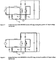
- a bridgeless boost converter comprises a first boost inductor L1 connected between a first AC input terminal and a first node 1 and a second boost inductor L2 connected between a second AC input terminal and a second node 2.
- a first boost diode Db1 is connected between the first node 1 and the positive output terminal Obp and a second boost diode Db2 is connected between the second node 2 and the positive output terminal Obp.
- a first boost switch Sb1 is connected in series with a first measuring unit, for example a first measuring resistor Rs1, between the first node 1 and a negative output terminal Obn.
- a second boost switch Sb2 is connected in series with a second measuring unit, for example a second measuring resistor Rs2, between the second node 2 and the negative output terminal Obn.
- a capacitor Cb is connected between the positive output terminal Obp and the negative output terminal Obn.
- a third measuring unit for example a third measuring resistor Rs3, is connected between the negative output terminal Obn and a third node 3.
- the first, second and third measuring units form a measuring system, indicated by a dotted rectangle in fig. 1 .
- a stabilization system indicated by a dotted rectangle in fig. 1 comprises a first impedance Zs1 connected between the third node 3 and the first AC input terminal and a second impedance Zs2 connected between the third node 3 and the second AC input terminal.
- the stabilization system comprises a first stabilization diode Dstab1 connected between the third node 3 and the first AC input terminal and a second stabilization diode connected between the third node 3 and the second AC input terminal.
- the switches are MOSFETs with intrinsic diodes.
- the switches are other types of switches with intrinsic diodes or switches connected in parallel with anti-parallel diodes.
- An example of alternative switches is IGBTs connected in parallel with anti-parallel diodes.
- the first measuring unit is measuring a value representing the current through the first switch Sb1, while the second measuring unit is measuring a value representing the current through the second switch Sb2. Moreover, the third measuring unit is measuring a value representing the sum of the currents through the components of the stabilization system.
- the measurements from the first, second and third measuring units are inputted to a control system, illustrated by the input signal u p .
- the computation of the input signal u p is shown in fig. 6 .
- the elements for computing the input signal up would normally be regarded as a part of the control system, i.e. the signals from the respective measuring units would be direct input to the control system.
- the voltage Vac is also inputted to the control system, as illustrated in fig. 5 .
- the voltage Vac is measured by means of a diode bridge, i.e. the only positive values of the voltage Vac is inputted to the control system.
- the control system is providing control signals to turn the switches Sb1 and Sb2 ON and OFF.
- the measurements above i.e. the signal u p and Vac, is used by the control system to control the switches so that the AC current is substantially in phase with the AC voltage and/or has the same wave shape as the AC input voltage, a common requirement for converters.
- the voltage Vac is then used as a reference value and the input signal u p is the measured value, where the control system controls the switches so that the input signal u p should be substantially equal to the reference value.
- the input signal u p can be computed by means of the voltages V Rs1 , V Rs2 , V Rs3 over the respective resistors Rs1, Rs2, Rs3 rather than the current through them. This is illustrated in fig. 7 . As illustrated, the measurements from the first, second and third measuring units are inputted to a control system, illustrated by the input signal u p .
Landscapes
- Engineering & Computer Science (AREA)
- Power Engineering (AREA)
- Physics & Mathematics (AREA)
- Electromagnetism (AREA)
- General Physics & Mathematics (AREA)
- Radar, Positioning & Navigation (AREA)
- Automation & Control Theory (AREA)
- Rectifiers (AREA)
- Dc-Dc Converters (AREA)
- Circuits Of Receivers In General (AREA)
- Control Of Motors That Do Not Use Commutators (AREA)
Priority Applications (2)
| Application Number | Priority Date | Filing Date | Title |
|---|---|---|---|
| SI200830772T SI2225822T1 (sl) | 2007-11-29 | 2008-11-21 | Nadzorni sistem in postopek nadzora ojačevalnega pretvornika brez mostička |
| PL08854373T PL2225822T3 (pl) | 2007-11-29 | 2008-11-21 | System sterowania oraz sposób sterowania bezmostkową przetwornicą podwyższającą napięcie |
Applications Claiming Priority (3)
| Application Number | Priority Date | Filing Date | Title |
|---|---|---|---|
| US99092307P | 2007-11-29 | 2007-11-29 | |
| GB0723402.4A GB2455128B (en) | 2007-11-29 | 2007-11-29 | Control system and method for controlling a bridgeless boost converter |
| PCT/NO2008/000415 WO2009070031A1 (en) | 2007-11-29 | 2008-11-21 | Control system and method for controlling a bridgeless boost converter |
Publications (3)
| Publication Number | Publication Date |
|---|---|
| EP2225822A1 EP2225822A1 (en) | 2010-09-08 |
| EP2225822B1 EP2225822B1 (en) | 2012-08-01 |
| EP2225822B2 true EP2225822B2 (en) | 2022-07-13 |
Family
ID=38962343
Family Applications (1)
| Application Number | Title | Priority Date | Filing Date |
|---|---|---|---|
| EP08854373.1A Not-in-force EP2225822B2 (en) | 2007-11-29 | 2008-11-21 | Control system and method for controlling a bridgeless boost converter |
Country Status (9)
| Country | Link |
|---|---|
| EP (1) | EP2225822B2 (es) |
| DK (1) | DK2225822T3 (es) |
| ES (1) | ES2392374T3 (es) |
| GB (1) | GB2455128B (es) |
| HR (1) | HRP20120836T1 (es) |
| PL (1) | PL2225822T3 (es) |
| PT (1) | PT2225822E (es) |
| SI (1) | SI2225822T1 (es) |
| WO (1) | WO2009070031A1 (es) |
Families Citing this family (3)
| Publication number | Priority date | Publication date | Assignee | Title |
|---|---|---|---|---|
| JP5640464B2 (ja) | 2009-07-29 | 2014-12-17 | Tdk株式会社 | スイッチング電源装置 |
| GB201317749D0 (en) | 2013-10-08 | 2013-11-20 | Dyson Technology Ltd | AC/DC boost converter |
| US10193437B1 (en) * | 2017-10-26 | 2019-01-29 | Semiconductor Components Industries, Llc | Bridgeless AC-DC converter with power factor correction and method therefor |
Family Cites Families (6)
| Publication number | Priority date | Publication date | Assignee | Title |
|---|---|---|---|---|
| GB721413A (en) | 1951-12-21 | 1955-01-05 | Onderzoekings Inst Res | Improvements in an extrusion press for thermoplastic material |
| GB721420A (en) | 1952-10-27 | 1955-01-05 | American Cyanamid Co | Improvements relating to the production of substantially uniform weight charges of apowder of slightly non-uniform density |
| US4412277A (en) | 1982-09-03 | 1983-10-25 | Rockwell International Corporation | AC-DC Converter having an improved power factor |
| US7164591B2 (en) * | 2003-10-01 | 2007-01-16 | International Rectifier Corporation | Bridge-less boost (BLB) power factor correction topology controlled with one cycle control |
| US20060198172A1 (en) | 2003-10-01 | 2006-09-07 | International Rectifier Corporation | Bridgeless boost converter with PFC circuit |
| US7355868B2 (en) | 2005-03-31 | 2008-04-08 | International Rectifier Corporation | Current sense method for bridgeless boost (BLB) PFC circuit using single current transformer |
-
2007
- 2007-11-29 GB GB0723402.4A patent/GB2455128B/en not_active Expired - Fee Related
-
2008
- 2008-11-21 ES ES08854373T patent/ES2392374T3/es active Active
- 2008-11-21 DK DK08854373.1T patent/DK2225822T3/da active
- 2008-11-21 WO PCT/NO2008/000415 patent/WO2009070031A1/en not_active Ceased
- 2008-11-21 PT PT08854373T patent/PT2225822E/pt unknown
- 2008-11-21 HR HRP20120836AT patent/HRP20120836T1/hr unknown
- 2008-11-21 PL PL08854373T patent/PL2225822T3/pl unknown
- 2008-11-21 SI SI200830772T patent/SI2225822T1/sl unknown
- 2008-11-21 EP EP08854373.1A patent/EP2225822B2/en not_active Not-in-force
Non-Patent Citations (4)
| Title |
|---|
| DE SOUZA A F ET AL: "High power factor rectifier with reduced conduction and commutation losses", TELECOMMUNICATIONENERGY CONFERENCE, 1999 † |
| INTELEC ’99. THE 21 ST INTERNATIONAL COPENHAGEN † |
| LU B ET AL: "Bridgeless PFC implementation using one cycle control technique", APPLIED POWER ELECTRONICSCONFERENCE AND EXPOSITION, 2005. APEC 2005 † |
| Lu B: "Investigation of High-density Integrated Solution for AC/DC Conversion of a Distributed Power System", dissertation submitted to the faculty of the Virginia Polytechnic Institute and State University, May 5, 2006 † |
Also Published As
| Publication number | Publication date |
|---|---|
| GB2455128A (en) | 2009-06-03 |
| EP2225822B1 (en) | 2012-08-01 |
| ES2392374T3 (es) | 2012-12-10 |
| WO2009070031A1 (en) | 2009-06-04 |
| PL2225822T3 (pl) | 2012-12-31 |
| EP2225822A1 (en) | 2010-09-08 |
| GB2455128B (en) | 2012-03-21 |
| PT2225822E (pt) | 2012-10-23 |
| SI2225822T1 (sl) | 2012-12-31 |
| HRP20120836T1 (hr) | 2012-11-30 |
| GB0723402D0 (en) | 2008-01-09 |
| DK2225822T3 (da) | 2012-11-12 |
Similar Documents
| Publication | Publication Date | Title |
|---|---|---|
| Kim et al. | Comparative performance analysis of high density and efficiency PFC topologies | |
| US9099934B2 (en) | Three phase active rectifier system | |
| Gong et al. | 6.6 kW three-phase interleaved totem pole PFC design with 98.9% peak efficiency for HEV/EV onboard charger | |
| CN110048597B (zh) | 功率因数校正电路的控制方法、控制器及系统 | |
| Itoh et al. | A novel three-phase PFC rectifier using a harmonic current injection method | |
| WO2010061654A1 (ja) | Pfcコンバータ | |
| CN101185044A (zh) | 功率因数校正的数字实现 | |
| US20060103342A1 (en) | Motor drive device for air conditioner | |
| EP4106167B1 (en) | Control circuit and ac-dc power supply applying the same | |
| US11736025B2 (en) | Electrical power conversion apparatus | |
| EP2218169B1 (en) | Bridgeless boost ac-dc converter | |
| EP2225822B2 (en) | Control system and method for controlling a bridgeless boost converter | |
| KR20100136086A (ko) | 무정전 직류 전원공급장치 | |
| Pathak et al. | 3-Phase Power Factor Correction using Vienna rectifier approach and modular construction for improved overall performance, efficiency and reliability | |
| US9036370B2 (en) | AC/DC power converter with improved power factor and improved THDi | |
| Liu et al. | Design and Implementation of Linear and Nonlinear Feedforward Controllers for High‐Performance Power Factor Corrected Circuits | |
| NO323385B1 (no) | Styringsmetode og anordning for omformer som benytter en TSSC | |
| KR101954636B1 (ko) | 간단한 고역률 스위칭 정류기의 제어회로 | |
| US20120275204A1 (en) | Bridgeless Power Factor Correcting Circuits with two Switches | |
| CN111327300B (zh) | 一种大功率交直流一体化的电子负载系统及其控制方法 | |
| Kannan et al. | A comparative study on different control techniques on bridgeless interleaved AC-DC converter for power factor correction | |
| Kalpana | High performance three-phase PFC rectifiers for telecom power supply | |
| Adedayo Ajenikoko et al. | Control Techniques and Power Factor Correction Methods: A Review | |
| Al-Baidhani et al. | Robust current-mode control of bridgeless single-switch SEPIC PFC converter | |
| Lange et al. | New unidirectional high-efficiency three-level single-phase bridgeless PFC rectifier |
Legal Events
| Date | Code | Title | Description |
|---|---|---|---|
| PUAI | Public reference made under article 153(3) epc to a published international application that has entered the european phase |
Free format text: ORIGINAL CODE: 0009012 |
|
| 17P | Request for examination filed |
Effective date: 20100629 |
|
| AK | Designated contracting states |
Kind code of ref document: A1 Designated state(s): AT BE BG CH CY CZ DE DK EE ES FI FR GB GR HR HU IE IS IT LI LT LU LV MC MT NL NO PL PT RO SE SI SK TR |
|
| AX | Request for extension of the european patent |
Extension state: AL BA MK RS |
|
| DAX | Request for extension of the european patent (deleted) | ||
| RBV | Designated contracting states (corrected) |
Designated state(s): AT BE BG CH CY CZ DE DK EE ES FI FR GR HR HU IE IS IT LI LT LU LV MC MT NL NO PL PT RO SE SI SK TR |
|
| GRAP | Despatch of communication of intention to grant a patent |
Free format text: ORIGINAL CODE: EPIDOSNIGR1 |
|
| GRAS | Grant fee paid |
Free format text: ORIGINAL CODE: EPIDOSNIGR3 |
|
| GRAA | (expected) grant |
Free format text: ORIGINAL CODE: 0009210 |
|
| AK | Designated contracting states |
Kind code of ref document: B1 Designated state(s): AT BE BG CH CY CZ DE DK EE ES FI FR GR HR HU IE IS IT LI LT LU LV MC MT NL NO PL PT RO SE SI SK TR |
|
| REG | Reference to a national code |
Ref country code: AT Ref legal event code: REF Ref document number: 569104 Country of ref document: AT Kind code of ref document: T Effective date: 20120815 Ref country code: CH Ref legal event code: EP |
|
| REG | Reference to a national code |
Ref country code: IE Ref legal event code: FG4D |
|
| REG | Reference to a national code |
Ref country code: DE Ref legal event code: R096 Ref document number: 602008017695 Country of ref document: DE Effective date: 20120927 |
|
| REG | Reference to a national code |
Ref country code: HR Ref legal event code: TUEP Ref document number: P20120836 Country of ref document: HR |
|
| REG | Reference to a national code |
Ref country code: PT Ref legal event code: SC4A Free format text: AVAILABILITY OF NATIONAL TRANSLATION Effective date: 20121015 Ref country code: SE Ref legal event code: TRGR |
|
| REG | Reference to a national code |
Ref country code: HR Ref legal event code: ODRP Ref document number: P20120836 Country of ref document: HR Payment date: 20121024 Year of fee payment: 5 |
|
| REG | Reference to a national code |
Ref country code: RO Ref legal event code: EPE |
|
| REG | Reference to a national code |
Ref country code: NL Ref legal event code: T3 |
|
| REG | Reference to a national code |
Ref country code: DK Ref legal event code: T3 |
|
| REG | Reference to a national code |
Ref country code: NO Ref legal event code: T2 Effective date: 20120801 |
|
| REG | Reference to a national code |
Ref country code: HR Ref legal event code: T1PR Ref document number: P20120836 Country of ref document: HR |
|
| REG | Reference to a national code |
Ref country code: ES Ref legal event code: FG2A Ref document number: 2392374 Country of ref document: ES Kind code of ref document: T3 Effective date: 20121210 |
|
| REG | Reference to a national code |
Ref country code: EE Ref legal event code: FG4A Ref document number: E007260 Country of ref document: EE Effective date: 20121031 |
|
| PGFP | Annual fee paid to national office [announced via postgrant information from national office to epo] |
Ref country code: DK Payment date: 20121120 Year of fee payment: 5 Ref country code: LU Payment date: 20121126 Year of fee payment: 5 |
|
| REG | Reference to a national code |
Ref country code: PL Ref legal event code: T3 |
|
| REG | Reference to a national code |
Ref country code: SK Ref legal event code: T3 Ref document number: E 12791 Country of ref document: SK |
|
| REG | Reference to a national code |
Ref country code: GR Ref legal event code: EP Ref document number: 20120402337 Country of ref document: GR Effective date: 20121122 |
|
| REG | Reference to a national code |
Ref country code: LT Ref legal event code: MG4D Effective date: 20120801 |
|
| PG25 | Lapsed in a contracting state [announced via postgrant information from national office to epo] |
Ref country code: CY Free format text: LAPSE BECAUSE OF FAILURE TO SUBMIT A TRANSLATION OF THE DESCRIPTION OR TO PAY THE FEE WITHIN THE PRESCRIBED TIME-LIMIT Effective date: 20120801 Ref country code: LT Free format text: LAPSE BECAUSE OF FAILURE TO SUBMIT A TRANSLATION OF THE DESCRIPTION OR TO PAY THE FEE WITHIN THE PRESCRIBED TIME-LIMIT Effective date: 20120801 Ref country code: IS Free format text: LAPSE BECAUSE OF FAILURE TO SUBMIT A TRANSLATION OF THE DESCRIPTION OR TO PAY THE FEE WITHIN THE PRESCRIBED TIME-LIMIT Effective date: 20121201 |
|
| PGFP | Annual fee paid to national office [announced via postgrant information from national office to epo] |
Ref country code: EE Payment date: 20121113 Year of fee payment: 5 Ref country code: IE Payment date: 20121120 Year of fee payment: 5 Ref country code: FI Payment date: 20121113 Year of fee payment: 5 Ref country code: CZ Payment date: 20121114 Year of fee payment: 5 Ref country code: HR Payment date: 20121024 Year of fee payment: 5 Ref country code: MC Payment date: 20121113 Year of fee payment: 5 Ref country code: BG Payment date: 20121113 Year of fee payment: 5 Ref country code: CH Payment date: 20121122 Year of fee payment: 5 |
|
| PG25 | Lapsed in a contracting state [announced via postgrant information from national office to epo] |
Ref country code: LV Free format text: LAPSE BECAUSE OF FAILURE TO SUBMIT A TRANSLATION OF THE DESCRIPTION OR TO PAY THE FEE WITHIN THE PRESCRIBED TIME-LIMIT Effective date: 20120801 |
|
| PGFP | Annual fee paid to national office [announced via postgrant information from national office to epo] |
Ref country code: SK Payment date: 20121119 Year of fee payment: 5 Ref country code: BE Payment date: 20121122 Year of fee payment: 5 Ref country code: ES Payment date: 20121127 Year of fee payment: 5 Ref country code: SI Payment date: 20121029 Year of fee payment: 5 Ref country code: GR Payment date: 20121128 Year of fee payment: 5 Ref country code: IT Payment date: 20121121 Year of fee payment: 5 Ref country code: SE Payment date: 20121120 Year of fee payment: 5 Ref country code: PT Payment date: 20121119 Year of fee payment: 5 Ref country code: TR Payment date: 20121101 Year of fee payment: 5 Ref country code: PL Payment date: 20121023 Year of fee payment: 5 |
|
| PGFP | Annual fee paid to national office [announced via postgrant information from national office to epo] |
Ref country code: NL Payment date: 20121120 Year of fee payment: 5 |
|
| PLBI | Opposition filed |
Free format text: ORIGINAL CODE: 0009260 |
|
| PLAX | Notice of opposition and request to file observation + time limit sent |
Free format text: ORIGINAL CODE: EPIDOSNOBS2 |
|
| 26 | Opposition filed |
Opponent name: ZTE CORPORATION Effective date: 20130430 |
|
| REG | Reference to a national code |
Ref country code: HU Ref legal event code: AG4A Ref document number: E015821 Country of ref document: HU |
|
| REG | Reference to a national code |
Ref country code: DE Ref legal event code: R026 Ref document number: 602008017695 Country of ref document: DE Effective date: 20130430 |
|
| PGFP | Annual fee paid to national office [announced via postgrant information from national office to epo] |
Ref country code: HU Payment date: 20121203 Year of fee payment: 5 |
|
| PLBB | Reply of patent proprietor to notice(s) of opposition received |
Free format text: ORIGINAL CODE: EPIDOSNOBS3 |
|
| PG25 | Lapsed in a contracting state [announced via postgrant information from national office to epo] |
Ref country code: MT Free format text: LAPSE BECAUSE OF FAILURE TO SUBMIT A TRANSLATION OF THE DESCRIPTION OR TO PAY THE FEE WITHIN THE PRESCRIBED TIME-LIMIT Effective date: 20120801 |
|
| REG | Reference to a national code |
Ref country code: HR Ref legal event code: PBON Ref document number: P20120836 Country of ref document: HR Effective date: 20131121 |
|
| REG | Reference to a national code |
Ref country code: PT Ref legal event code: MM4A Free format text: LAPSE DUE TO NON-PAYMENT OF FEES Effective date: 20140521 |
|
| BERE | Be: lapsed |
Owner name: ELTEK VALERE AS Effective date: 20131130 |
|
| REG | Reference to a national code |
Ref country code: NL Ref legal event code: V1 Effective date: 20140601 |
|
| REG | Reference to a national code |
Ref country code: DK Ref legal event code: EBP Effective date: 20131130 |
|
| REG | Reference to a national code |
Ref country code: CH Ref legal event code: PL |
|
| REG | Reference to a national code |
Ref country code: SE Ref legal event code: EUG |
|
| PG25 | Lapsed in a contracting state [announced via postgrant information from national office to epo] |
Ref country code: MC Free format text: LAPSE BECAUSE OF NON-PAYMENT OF DUE FEES Effective date: 20131202 Ref country code: EE Free format text: LAPSE BECAUSE OF NON-PAYMENT OF DUE FEES Effective date: 20131130 Ref country code: LI Free format text: LAPSE BECAUSE OF NON-PAYMENT OF DUE FEES Effective date: 20131130 Ref country code: CH Free format text: LAPSE BECAUSE OF NON-PAYMENT OF DUE FEES Effective date: 20131130 |
|
| REG | Reference to a national code |
Ref country code: GR Ref legal event code: ML Ref document number: 20120402337 Country of ref document: GR Effective date: 20140603 |
|
| REG | Reference to a national code |
Ref country code: SK Ref legal event code: MM4A Ref document number: E 12791 Country of ref document: SK Effective date: 20131121 |
|
| REG | Reference to a national code |
Ref country code: EE Ref legal event code: MM4A Ref document number: E007260 Country of ref document: EE Effective date: 20131130 |
|
| REG | Reference to a national code |
Ref country code: IE Ref legal event code: MM4A |
|
| PG25 | Lapsed in a contracting state [announced via postgrant information from national office to epo] |
Ref country code: SI Free format text: LAPSE BECAUSE OF NON-PAYMENT OF DUE FEES Effective date: 20131122 Ref country code: PT Free format text: LAPSE BECAUSE OF NON-PAYMENT OF DUE FEES Effective date: 20140521 Ref country code: SE Free format text: LAPSE BECAUSE OF NON-PAYMENT OF DUE FEES Effective date: 20131122 Ref country code: SK Free format text: LAPSE BECAUSE OF NON-PAYMENT OF DUE FEES Effective date: 20131121 Ref country code: IT Free format text: LAPSE BECAUSE OF NON-PAYMENT OF DUE FEES Effective date: 20131121 Ref country code: CZ Free format text: LAPSE BECAUSE OF NON-PAYMENT OF DUE FEES Effective date: 20131121 Ref country code: GR Free format text: LAPSE BECAUSE OF NON-PAYMENT OF DUE FEES Effective date: 20140603 Ref country code: NL Free format text: LAPSE BECAUSE OF NON-PAYMENT OF DUE FEES Effective date: 20140601 Ref country code: FI Free format text: LAPSE BECAUSE OF NON-PAYMENT OF DUE FEES Effective date: 20131121 |
|
| REG | Reference to a national code |
Ref country code: SI Ref legal event code: KO00 Effective date: 20140714 |
|
| PG25 | Lapsed in a contracting state [announced via postgrant information from national office to epo] |
Ref country code: HU Free format text: LAPSE BECAUSE OF NON-PAYMENT OF DUE FEES Effective date: 20131122 Ref country code: HR Free format text: LAPSE BECAUSE OF NON-PAYMENT OF DUE FEES Effective date: 20131121 Ref country code: BE Free format text: LAPSE BECAUSE OF NON-PAYMENT OF DUE FEES Effective date: 20131130 |
|
| PG25 | Lapsed in a contracting state [announced via postgrant information from national office to epo] |
Ref country code: DK Free format text: LAPSE BECAUSE OF NON-PAYMENT OF DUE FEES Effective date: 20131130 Ref country code: IE Free format text: LAPSE BECAUSE OF NON-PAYMENT OF DUE FEES Effective date: 20131121 |
|
| REG | Reference to a national code |
Ref country code: AT Ref legal event code: MM01 Ref document number: 569104 Country of ref document: AT Kind code of ref document: T Effective date: 20131121 |
|
| PG25 | Lapsed in a contracting state [announced via postgrant information from national office to epo] |
Ref country code: RO Free format text: LAPSE BECAUSE OF NON-PAYMENT OF DUE FEES Effective date: 20131121 |
|
| PG25 | Lapsed in a contracting state [announced via postgrant information from national office to epo] |
Ref country code: AT Free format text: LAPSE BECAUSE OF NON-PAYMENT OF DUE FEES Effective date: 20131121 Ref country code: PL Free format text: LAPSE BECAUSE OF NON-PAYMENT OF DUE FEES Effective date: 20131121 |
|
| REG | Reference to a national code |
Ref country code: ES Ref legal event code: FD2A Effective date: 20150327 |
|
| PG25 | Lapsed in a contracting state [announced via postgrant information from national office to epo] |
Ref country code: ES Free format text: LAPSE BECAUSE OF NON-PAYMENT OF DUE FEES Effective date: 20131122 |
|
| PG25 | Lapsed in a contracting state [announced via postgrant information from national office to epo] |
Ref country code: BG Free format text: LAPSE BECAUSE OF NON-PAYMENT OF DUE FEES Effective date: 20131130 Ref country code: LU Free format text: LAPSE BECAUSE OF NON-PAYMENT OF DUE FEES Effective date: 20131121 |
|
| PG25 | Lapsed in a contracting state [announced via postgrant information from national office to epo] |
Ref country code: TR Free format text: LAPSE BECAUSE OF NON-PAYMENT OF DUE FEES Effective date: 20131121 |
|
| REG | Reference to a national code |
Ref country code: FR Ref legal event code: PLFP Year of fee payment: 8 |
|
| RDAF | Communication despatched that patent is revoked |
Free format text: ORIGINAL CODE: EPIDOSNREV1 |
|
| APBM | Appeal reference recorded |
Free format text: ORIGINAL CODE: EPIDOSNREFNO |
|
| APBP | Date of receipt of notice of appeal recorded |
Free format text: ORIGINAL CODE: EPIDOSNNOA2O |
|
| APAH | Appeal reference modified |
Free format text: ORIGINAL CODE: EPIDOSCREFNO |
|
| APBQ | Date of receipt of statement of grounds of appeal recorded |
Free format text: ORIGINAL CODE: EPIDOSNNOA3O |
|
| REG | Reference to a national code |
Ref country code: FR Ref legal event code: PLFP Year of fee payment: 9 |
|
| REG | Reference to a national code |
Ref country code: FR Ref legal event code: PLFP Year of fee payment: 10 |
|
| PG25 | Lapsed in a contracting state [announced via postgrant information from national office to epo] |
Ref country code: BG Free format text: LAPSE BECAUSE OF NON-PAYMENT OF DUE FEES Effective date: 20170808 |
|
| APBU | Appeal procedure closed |
Free format text: ORIGINAL CODE: EPIDOSNNOA9O |
|
| PGFP | Annual fee paid to national office [announced via postgrant information from national office to epo] |
Ref country code: FR Payment date: 20211122 Year of fee payment: 14 Ref country code: DE Payment date: 20211118 Year of fee payment: 14 |
|
| PUAH | Patent maintained in amended form |
Free format text: ORIGINAL CODE: 0009272 |
|
| STAA | Information on the status of an ep patent application or granted ep patent |
Free format text: STATUS: PATENT MAINTAINED AS AMENDED |
|
| 27A | Patent maintained in amended form |
Effective date: 20220713 |
|
| AK | Designated contracting states |
Kind code of ref document: B2 Designated state(s): AT BE BG CH CY CZ DE DK EE ES FI FR GR HR HU IE IS IT LI LT LU LV MC MT NL NO PL PT RO SE SI SK TR |
|
| REG | Reference to a national code |
Ref country code: DE Ref legal event code: R102 Ref document number: 602008017695 Country of ref document: DE |
|
| PGFP | Annual fee paid to national office [announced via postgrant information from national office to epo] |
Ref country code: NO Payment date: 20220921 Year of fee payment: 15 |
|
| REG | Reference to a national code |
Ref country code: NO Ref legal event code: TB2 |
|
| PG25 | Lapsed in a contracting state [announced via postgrant information from national office to epo] |
Ref country code: GR Free format text: LAPSE BECAUSE OF FAILURE TO SUBMIT A TRANSLATION OF THE DESCRIPTION OR TO PAY THE FEE WITHIN THE PRESCRIBED TIME-LIMIT Effective date: 20221014 |
|
| REG | Reference to a national code |
Ref country code: DE Ref legal event code: R119 Ref document number: 602008017695 Country of ref document: DE |
|
| PG25 | Lapsed in a contracting state [announced via postgrant information from national office to epo] |
Ref country code: DE Free format text: LAPSE BECAUSE OF NON-PAYMENT OF DUE FEES Effective date: 20230601 |
|
| PG25 | Lapsed in a contracting state [announced via postgrant information from national office to epo] |
Ref country code: FR Free format text: LAPSE BECAUSE OF NON-PAYMENT OF DUE FEES Effective date: 20221130 |
|
| PG25 | Lapsed in a contracting state [announced via postgrant information from national office to epo] |
Ref country code: NO Free format text: LAPSE BECAUSE OF NON-PAYMENT OF DUE FEES Effective date: 20231130 |