EP2224468B1 - Plasma processing apparatus, plasma processing method - Google Patents
Plasma processing apparatus, plasma processing method Download PDFInfo
- Publication number
- EP2224468B1 EP2224468B1 EP10166701.2A EP10166701A EP2224468B1 EP 2224468 B1 EP2224468 B1 EP 2224468B1 EP 10166701 A EP10166701 A EP 10166701A EP 2224468 B1 EP2224468 B1 EP 2224468B1
- Authority
- EP
- European Patent Office
- Prior art keywords
- substrate
- plasma
- antenna
- container
- high frequency
- Prior art date
- Legal status (The legal status is an assumption and is not a legal conclusion. Google has not performed a legal analysis and makes no representation as to the accuracy of the status listed.)
- Expired - Lifetime
Links
- 238000003672 processing method Methods 0.000 title claims description 9
- 239000000758 substrate Substances 0.000 claims description 75
- VYPSYNLAJGMNEJ-UHFFFAOYSA-N Silicium dioxide Chemical compound O=[Si]=O VYPSYNLAJGMNEJ-UHFFFAOYSA-N 0.000 claims description 10
- 229910052581 Si3N4 Inorganic materials 0.000 claims description 8
- HQVNEWCFYHHQES-UHFFFAOYSA-N silicon nitride Chemical compound N12[Si]34N5[Si]62N3[Si]51N64 HQVNEWCFYHHQES-UHFFFAOYSA-N 0.000 claims description 8
- 229910052814 silicon oxide Inorganic materials 0.000 claims description 8
- 238000000151 deposition Methods 0.000 description 36
- 230000008021 deposition Effects 0.000 description 36
- 239000007789 gas Substances 0.000 description 35
- 238000005268 plasma chemical vapour deposition Methods 0.000 description 21
- 230000000694 effects Effects 0.000 description 16
- 230000004907 flux Effects 0.000 description 16
- 230000006378 damage Effects 0.000 description 15
- 239000000463 material Substances 0.000 description 15
- 238000005530 etching Methods 0.000 description 13
- 239000002245 particle Substances 0.000 description 13
- 238000013021 overheating Methods 0.000 description 11
- 150000002500 ions Chemical class 0.000 description 10
- PNEYBMLMFCGWSK-UHFFFAOYSA-N aluminium oxide Inorganic materials [O-2].[O-2].[O-2].[Al+3].[Al+3] PNEYBMLMFCGWSK-UHFFFAOYSA-N 0.000 description 8
- BLRPTPMANUNPDV-UHFFFAOYSA-N Silane Chemical compound [SiH4] BLRPTPMANUNPDV-UHFFFAOYSA-N 0.000 description 7
- 239000004065 semiconductor Substances 0.000 description 5
- XKRFYHLGVUSROY-UHFFFAOYSA-N Argon Chemical compound [Ar] XKRFYHLGVUSROY-UHFFFAOYSA-N 0.000 description 4
- 238000005229 chemical vapour deposition Methods 0.000 description 4
- 229910052593 corundum Inorganic materials 0.000 description 4
- 238000000034 method Methods 0.000 description 4
- 230000007935 neutral effect Effects 0.000 description 4
- 229910001845 yogo sapphire Inorganic materials 0.000 description 4
- 238000006243 chemical reaction Methods 0.000 description 3
- 230000003247 decreasing effect Effects 0.000 description 3
- 239000012212 insulator Substances 0.000 description 3
- 229910000077 silane Inorganic materials 0.000 description 3
- UFHFLCQGNIYNRP-UHFFFAOYSA-N Hydrogen Chemical compound [H][H] UFHFLCQGNIYNRP-UHFFFAOYSA-N 0.000 description 2
- XAGFODPZIPBFFR-UHFFFAOYSA-N aluminium Chemical compound [Al] XAGFODPZIPBFFR-UHFFFAOYSA-N 0.000 description 2
- 229910052782 aluminium Inorganic materials 0.000 description 2
- 229910052786 argon Inorganic materials 0.000 description 2
- QVGXLLKOCUKJST-UHFFFAOYSA-N atomic oxygen Chemical compound [O] QVGXLLKOCUKJST-UHFFFAOYSA-N 0.000 description 2
- 239000001307 helium Substances 0.000 description 2
- 229910052734 helium Inorganic materials 0.000 description 2
- SWQJXJOGLNCZEY-UHFFFAOYSA-N helium atom Chemical compound [He] SWQJXJOGLNCZEY-UHFFFAOYSA-N 0.000 description 2
- 239000001257 hydrogen Substances 0.000 description 2
- 229910052739 hydrogen Inorganic materials 0.000 description 2
- 238000009616 inductively coupled plasma Methods 0.000 description 2
- 239000011261 inert gas Substances 0.000 description 2
- 239000001301 oxygen Substances 0.000 description 2
- 229910052760 oxygen Inorganic materials 0.000 description 2
- 238000004380 ashing Methods 0.000 description 1
- 229910052681 coesite Inorganic materials 0.000 description 1
- 239000000470 constituent Substances 0.000 description 1
- 229910052906 cristobalite Inorganic materials 0.000 description 1
- 230000001419 dependent effect Effects 0.000 description 1
- 239000011810 insulating material Substances 0.000 description 1
- 238000004519 manufacturing process Methods 0.000 description 1
- 229910021424 microcrystalline silicon Inorganic materials 0.000 description 1
- 239000000377 silicon dioxide Substances 0.000 description 1
- 239000007858 starting material Substances 0.000 description 1
- 229910052682 stishovite Inorganic materials 0.000 description 1
- 229910052905 tridymite Inorganic materials 0.000 description 1
Images


Classifications
-
- H—ELECTRICITY
- H01—ELECTRIC ELEMENTS
- H01J—ELECTRIC DISCHARGE TUBES OR DISCHARGE LAMPS
- H01J37/00—Discharge tubes with provision for introducing objects or material to be exposed to the discharge, e.g. for the purpose of examination or processing thereof
- H01J37/32—Gas-filled discharge tubes
- H01J37/32009—Arrangements for generation of plasma specially adapted for examination or treatment of objects, e.g. plasma sources
- H01J37/32082—Radio frequency generated discharge
- H01J37/321—Radio frequency generated discharge the radio frequency energy being inductively coupled to the plasma
-
- C—CHEMISTRY; METALLURGY
- C23—COATING METALLIC MATERIAL; COATING MATERIAL WITH METALLIC MATERIAL; CHEMICAL SURFACE TREATMENT; DIFFUSION TREATMENT OF METALLIC MATERIAL; COATING BY VACUUM EVAPORATION, BY SPUTTERING, BY ION IMPLANTATION OR BY CHEMICAL VAPOUR DEPOSITION, IN GENERAL; INHIBITING CORROSION OF METALLIC MATERIAL OR INCRUSTATION IN GENERAL
- C23C—COATING METALLIC MATERIAL; COATING MATERIAL WITH METALLIC MATERIAL; SURFACE TREATMENT OF METALLIC MATERIAL BY DIFFUSION INTO THE SURFACE, BY CHEMICAL CONVERSION OR SUBSTITUTION; COATING BY VACUUM EVAPORATION, BY SPUTTERING, BY ION IMPLANTATION OR BY CHEMICAL VAPOUR DEPOSITION, IN GENERAL
- C23C16/00—Chemical coating by decomposition of gaseous compounds, without leaving reaction products of surface material in the coating, i.e. chemical vapour deposition [CVD] processes
- C23C16/44—Chemical coating by decomposition of gaseous compounds, without leaving reaction products of surface material in the coating, i.e. chemical vapour deposition [CVD] processes characterised by the method of coating
- C23C16/50—Chemical coating by decomposition of gaseous compounds, without leaving reaction products of surface material in the coating, i.e. chemical vapour deposition [CVD] processes characterised by the method of coating using electric discharges
- C23C16/505—Chemical coating by decomposition of gaseous compounds, without leaving reaction products of surface material in the coating, i.e. chemical vapour deposition [CVD] processes characterised by the method of coating using electric discharges using radio frequency discharges
- C23C16/507—Chemical coating by decomposition of gaseous compounds, without leaving reaction products of surface material in the coating, i.e. chemical vapour deposition [CVD] processes characterised by the method of coating using electric discharges using radio frequency discharges using external electrodes, e.g. in tunnel type reactors
Definitions
- This invention relates to a plasma processing apparatus, and a plasma processing method which generate a plasma to process a substrate.
- the plasma CVD apparatus is an apparatus in which a material gas serving as a starting material for a film is introduced into a film deposition chamber within a tubular container, a high frequency is shot from a high frequency antenna to convert the material gas into the state of a plasma, and active excited atoms in the plasma promote a chemical reaction on the surface of a substrate to carry out film deposition.
- the high frequency antenna in the shape of a flat ring is disposed on the top of a ceiling surface opposed to the substrate, and power is supplied to the high frequency antenna to shoot a high frequency wave into the tubular container.
- a plasma processing apparatus is disclosed, for example, in Japanese Patent No. 3,172,340 .
- the plasma density is so high that a voltage is applied to the electrode on the surface of the semiconductor owing to a potential difference of space, incurring the risk of destroying the semiconductor device (device destruction due to a charging effect).
- a plasma processing apparatus capable of suppressing device destruction due to the charging effect.
- US 2002/007794 A1 discloses a plasma processing apparatus having a ring-shaped antenna disposed at a top of a ceiling surface of a processing chamber.
- a very high frequency power having a frequency of 20 MHz to 300 MHz can be applied to the antenna, thereby generating a high dense plasma having an electron temperature from 1.5 to 2.5 eV.
- An object of the present invention is to provide a plasma processing apparatus and a plasma-processing method which can suppress device destruction due to the charging effect.
- the present invention provides a plasma processing apparatus for forming a film of silicon oxide or silicon nitride on a surface of a substrate as defined in claim 1 and a plasma processing method for forming a film of silicon oxide or silicon nitride on a surface of a substrate as defined in claim 4.
- Preferred embodiments are defined in the dependent claims.
- the substrate can be located in a region where the plasma has a low electron temperature even though the plasma has a high density. Since the substrate is located in the region where the electron temperature is low even though the electron density is high, device destruction of the substrate due to the charging effect can be suppressed.
- the region where the plasma has the high density has an electron density such that there are 1, 0e10 electrons or more per cm 3
- the region where the plasma has the low electron temperature is a region where the electron temperature is 1 electronvolt or less.
- the distance from a lower surface of the antenna to the substrate is set at more than 200 mm.
- the substrate can be located in a region where the plasma has a low electron temperature even though the plasma has a high density. Since the substrate is located in the region where the electron temperature is low even though the electron density is high, device destruction of the substrate due to the charging effect can be suppressed reliably.
- the substrate can be located in a region where the electron temperature is low even though the electron density is high. Since the region has a low electron temperature, device destruction of the substrate due to the charging effect can be suppressed.
- the present example is a plasma film deposition apparatus in which a source gas (a material gas: e.g., SiH 4 ) is supplied into a film deposition chamber, and a plasma is generated to excite and activate atoms and molecules, which form a film of silicon oxide or silicon nitride on the surface of a substrate.
- a source gas a material gas: e.g., SiH 4
- a plasma is generated to excite and activate atoms and molecules, which form a film of silicon oxide or silicon nitride on the surface of a substrate.
- power is supplied from above the top of a ceiling surface to a flat ring-shaped antenna to generate a plasma within a tubular container under an inductively coupled system, thereby forming the film of silicon oxide or silicon nitride on the surface of the substrate.
- an electric current flowing in a direction opposite to the direction of a feed current for generating the plasma is generated outwardly of the ceiling surface, whereby a magnetic flux density in the direction of the wall surface at the position of the wall is decreased to suppress impingement of electrons and ions on the wall of the tubular container.
- a uniform plasma can be generated over a wide range within the tubular container with the use of the antenna having a diameter fitting the diameter of the tubular container.
- the magnetic flux density in the direction of the wall surface can be decreased to suppress overheating, and suppress the occurrence of particles by an etching action.
- the present example can also be applied to a plasma processing apparatus in which a plasma is generated, and atoms and molecules excited and activated thereby apply processing, such as etching, to the surface of the substrate.
- a plasma CVD apparatus 1 is furnished with a tubular container (container) 2 of a cylindrical shape and made of aluminum, and a film deposition chamber 3 is formed within the container 2.
- a circular ceiling plate 4 made of an insulating material (for example, alumina: Al 2 O 3 ) is provided at the top of the container 2, and a wafer support base 5 is provided in the film deposition chamber 3 at the center of the container 2.
- the wafer support base 5 has a disk-shaped bearing portion 7 for holding a semiconductor substrate 6, and the bearing portion 7 is supported by a support shaft 8.
- a high frequency antenna 11 for example, in the form of a circular coil ring (flat ring) is placed on the ceiling plate 4, and a high frequency power source 12 (alternating current power source) is connected (power supply means) to the high frequency antenna 11 via a matching instrument (not shown). Electric power is supplied to the high frequency antenna, whereby an electromagnetic wave is thrown into the film deposition chamber 3 of the container 2. The electromagnetic wave, thrown into the container 2, ionizes a gas within the film deposition chamber 3 to generate a plasma.
- a high frequency power source 12 alternating current power source
- the container 2 is provided with, for example, gas supply nozzles 13 as source gas supply means for supplying a material gas, such as silane (for example, SiH 4 ).
- a source gas which serves as a material for film deposition (for example, Si) is supplied through the gas supply nozzles 13 into the film deposition chamber 3.
- the container 2 is also provided with auxiliary gas supply nozzles (not shown), which are made of an insulator material (for example, alumina: Al 2 O 3 ), for supplying an inert gas (rare gas) such as argon or helium, or an auxiliary gas such as oxygen or hydrogen.
- the interior of the container 2 is maintained at a predetermined pressure by a vacuum device 14.
- the container 2 is also provided with a carry-in/carry-out port for the substrate 6, although the carry-in/carry-out port is not shown. Through this carry-in/carry-out port, the substrate 6 is carried from a transport chamber (not shown) into the container 2, and carried out of the container 2 to the transport chamber.
- the substrate 6 is placed on the bearing portion 7 of the wafer support base 5, and held (by, for example, an electrostatic chuck).
- a predetermined flow rate of the source gas is supplied through the gas supply nozzles 13 into the film deposition chamber 3, and also a predetermined flow rate of the auxiliary gas is supplied through the auxiliary gas supply nozzles into the film deposition chamber 3, with the interior of the film deposition chamber 3 being set at a predetermined pressure suitable for the conditions for film deposition.
- electric power is supplied from the high frequency power source 12 to the high frequency antenna 11 to generate a high frequency wave.
- the material gas within the film deposition chamber 3 is electrically discharged to be partly turned into the state of a plasma.
- This plasma impinges on other neutral molecules in the material gas to ionize or excite the neutral molecules further.
- the thus produced active particles are adsorbed onto the surface of the substrate 6 to cause a chemical reaction with good efficiency, whereby they are deposited to form a CVD film.
- a second antenna is disposed around an outer part of the antenna on the ceiling surface, whereby an electric current flowing in a direction opposite to the direction of the electric current fed to the antenna is supplied to the second antenna.
- the high frequency antenna 11 is made up of an antenna 11a which is a portion of nearly the same diameter as that of the ceil ing surface, and a second antenna 11b which is a portion located outwardly of the ceiling surface.
- An electric current is supplied from the high frequency power source 12 to the site of the second antenna 11b in a state of connection opposite to that for the site of the antenna 11a (i.e., second power supply means).
- the high frequency power source 12 is connected to the coil on the grounded side at the site of the antenna 11a, so that the coil at the site of the antenna 11a on a side, where the high frequency power source 12 is connected, is brought into a grounded state.
- lines of magnetic force, F2 heading in a direction opposite to the direction of lines of magnetic force, F1, appearing at the site of the antenna 11a are generated at the site of the second antenna 11b.
- the lines F1 of magnetic force passing through the wall (tubular surface) of the container 2 are merged with the lines F2 of magnetic force heading in the opposite direction to decrease the lines of magnetic force passing through the wall (tubular surface) of the container 2.
- the magnetic flux density in the direction of the wall surface at the position of the wall of the container 2 is lowered. This resolves the problem that the electrons and ions impinge on the wall of the container 2, thereby causing overheating or causing the occurrence of particles by an etching action.
- the antenna 12a has nearly the same diameter as the diameter of the ceiling surface.
- a uniform plasma can be generated over a wide range relative to the size of the container, there is no decrease in the efficiency, and the uniformity of the plasma within the container 2 can be maintained.
- the plasma CVD apparatus 1 is constituted such that even when a uniform plasma is generated over a wide range within the container 2, the magnetic flux density in the direction of the wall surface can be rendered low, overheating can be avoided, and the occurrence of particles by an etching action can be prevented.
- FIGS. 3 to 5 Other examples of the plasma CVD apparatuses equipped with antennas and power supply means according to other examples will be described based on FIGS. 3 to 5 . Constituent members other than the antenna and power supply means are the same as those in FIG. 1 . Thus, explanations will be offered by reference to the plan views of FIGS. 3 to 5 corresponding to FIG. 2 , and descriptions of the features of the same portions are omitted.
- a high frequency antenna 11, as an antenna is the same as that in FIGS. 1 and 2 in terms of its feature, and is in the form of a flat coil.
- a high frequency power source 12 is connected to the site of the antenna 11a, while a second high frequency power source 21 as second power supplymeans is connected to the site of a second antenna 11b.
- An electric current is supplied from the second high frequency power source 21 to the site of the second antenna 11b in a state of connection opposite to that for the site of the antenna 11a.
- the high frequency power source 12 is connected to the coil on the grounded side at the site of the antenna 11a, so that the coil at the site of the antenna 11a on a side, where the high frequency power source 12 is connected, is brought into a grounded state.
- lines of magnetic force, F2 heading in a direction opposite to the direction of lines of magnetic force, F1, appearing at the site of the antenna 11a are generated at the site of the second antenna 11b, as in the example shown in FIG. 1 .
- the lines F1 of magnetic force passing through the wall (tubular surface) of the container 2 are merged with the lines F2 of magnetic force heading in the opposite direction to decrease the lines of magnetic force passing through the wall (tubular surface) of the container 2.
- the magnetic flux density in the direction of the wall surface at the position of the wall of the container 2 is lowered. This resolves the problem that the electrons and ions impinge on the wall of the container 2, thereby causing overheating or causing the occurrence of particles by an etching action.
- the antenna 11a has nearly the same diameter as the diameter of the ceiling surface.
- a uniform plasma can be generated over a wide range relative to the size of the container, there is no decrease in the efficiency, and the uniformity of the plasma within the container 2 can be maintained.
- the plasma CVD apparatus is constituted such that even when a uniform plasma is generated over a wide range within the container 2, the magnetic flux density in the direction of the wall surface can be rendered low, overheating can be avoided, and the occurrence of particles by an etching action can be prevented.
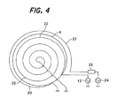
- a third example will be described based on FIG. 4 .
- a flat coil-shaped high frequency antenna 22, as an antenna having nearly the same diameter as the diameter of a ceiling plate 4, is disposed.
- a second antenna 23, having a different feature from that of the high frequency antenna 22, is disposed outside of the high frequency antenna 22, namely, outwardly of the ceiling surface.
- a high frequency power source 12 is connected to the high frequency antenna 22, while a second high frequency power source 24 as second power supply means is connected to the second antenna 23.
- the high frequency antenna 22 and the second high frequency power source 24 are connected to the high frequency power source 12 and the second high frequency power source 24 in the same direction.
- the second high frequency power source 24 is connected to the second antenna 23 via a phase shifter 25 as phase changing means.
- An electric current of a phase opposite to that of an electric current fed from the high frequency power source 12 to the high frequency antenna 22 is supplied from the second high frequency power source 24 to the second antenna 23 via the phase shifter 25. Because of this feature, lines of magnetic force heading in a direction opposite to the direction of lines of magnetic force appearing at the site of the high frequency antenna 22 are generated at the site of the second antenna 23, as in the example shown in FIG. 1 .
- the lines of magnetic force passing through the wall (tubular surface) of the container 2 are merged with the lines of magnetic force heading in the opposite direction to decrease the lines of magnetic force passing through the wall (tubular surface) of the container 2.
- the magnetic flux density in the direction of the wall surface at the position of the wall of the container 2 is lowered. This resolves the problem that the electrons and ions impinge on the wall of the container 2, thereby causing overheating or causing the occurrence of particles by an etching action.
- the high frequency antenna 22 has nearly the same diameter as the diameter of the ceiling surface.
- a uniform plasma can be generated over a wide range relative to the size of the container 2, there is no decrease in the efficiency, and the uniformity of the plasma within the container 2 can be maintained.
- the plasma CVD apparatus is constituted such that even when a uniform plasma is generated over a wide range within the container 2, the magnetic flux density in the direction of the wall surface can be rendered low, overheating can be avoided, and the occurrence of particles by an etching action can be prevented.
- a fourth example will be described based on FIG. 5 .
- a high frequency antenna 31 whichhas nearly the same diameter as the diameter of a ceiling plate 4, is composed of antennas 31a, 31b, 31c and 31d each in the form of a concentric ring.
- a ring-shaped second antenna 32 is disposed outside of the high frequency antenna 31, namely, outwardly of the ceiling surface.
- a high frequency power source 12 is connected in parallel to the antennas 31a, 31b, 31c, 31d, and the second antenna 32 is connected to the high frequency power source 12 in a state of connection opposite to that for the ring antenna 31. That is, the second antenna 32 is connected to the high frequency power source 12 in a state opposite to the state of connection of the antenna 31 to the high frequency power source 12, namely, such that the connected side and the grounded side for the second antenna 32 are opposite to those for the antenna 31.
- the antenna 31 has nearly the same diameter as the diameter of the ceiling surface.
- a uniform plasma can be generated over a wide range relative to the size of the container 2, there is no decrease in the efficiency, and the uniformity of the plasma within the container 2 can be maintained.
- the plasma CVD apparatus is constituted such that even when a uniform plasma is generated over a wide range within the container 2, the magnetic flux density in the direction of the wall surface can be rendered low, overheating can be avoided, and the occurrence of particles by an etching action can be prevented.
- the present invention is a plasma film deposition apparatus in which a source gas (a material gas: e.g., SiH 4 ) is supplied into a film deposition chamber, and a plasma is generated to excite and activate atoms and molecules, which form a film of silicon oxide or silicon nitride on the surface of a substrate.
- a source gas a material gas: e.g., SiH 4
- a plasma is generated to excite and activate atoms and molecules, which form a film of silicon oxide or silicon nitride on the surface of a substrate.
- power is supplied from above the top of a ceiling surface to a ring-shaped antenna to generate a plasma within a tubular container under an inductively coupled system, thereby forming a film of silicon oxide or silicon nitride on the surface of the substrate.
- the substrate is located in a region where the plasma has a low electron temperature even when the plasma has a high density.
- the region where the plasma is at a high density has an electron density such that there are 1,0e10 electrons or more per cm 3 .
- the region where the plasma is at a low electron temperature is a region where the electron temperature is 1 electronvolt or less.
- a high frequency power source of 10 MHz to 30 MHz is connected to an antenna, and the distance from the lower surface of the antenna to a substrate is set at more than 200 mm in order to locate the substrate in a region where the electron temperature is 1 electronvolt or less.
- the substrate is located in a region where the electron temperature is low even though the electron density is high. Since the region has a low electron temperature, device destruction due to the charging effect can be suppressed.
- a plasma processing apparatus in which a plasma is generated to excite and activate atoms and molecules, which apply processing, such as etching or ashing, to the surface of a substrate.
- plasma film deposition apparatus plasma CVD apparatus
- a plasma CVD apparatus 81 is furnished with a tubular container (container) 82 of a cylindrical shape and made of aluminum, and a film deposition chamber 83 (for example, diameter 250 mm to 500 mm) is formed within the container 82.
- a circular ceiling plate 84 made of an insulator material (for example, alumina: Al 2 O 3 , thickness 30 mm) is provided at the top of the container 82, and a wafer support base 85 is provided in the film deposition chamber 83 at the center of the container 82.
- the wafer support base 85 has a disk-sh aped bearing portion 87 for holding a semiconductor substrate 86, and the substrate 86 is held on the bearing portion 7, for example, by electrostatic chuck means 88.
- a high frequency antenna 91 as an antenna, for example, in the form of a circular coil ring (flat ring), is placed on the ceiling plate 84, and a high frequency power source 92 (alternating current power source) is connected (high frequency source) to the high frequency antenna 91 via a matching instrument (not shown). Electric power is supplied to the high frequency antenna 91, whereby an electromagnetic wave is thrown into the film deposition chamber 83 of the container 82. The electromagnetic wave, thrown into the container 82, ionizes a gas within the film deposition chamber 83 to generate a plasma.
- a high frequency power source 92 alternating current power source
- the high frequency source with an output of 2 kW to 15 kW (e.g., 5 kW) and a frequency of 10 MHz to 30 MHz (e.g., 13.56 MHz) is connected to the high frequency antenna 91.
- the container 82 is provided with, for example, gas supply nozzles 13 for supplying a material gas, such as silane (for example, SiH 4 ).
- a source gas which serves as a material for film deposition (for example, SiO 2 ), is supplied through the gas supply nozzles 13 into the film deposition chamber 3.
- the container 2 is also provided with auxiliary gas supply nozzles (not shown), which are made of an insulator material (for example, alumina: Al 2 O 3 ), for supplying an inert gas (rare gas) such as argon or helium, or an auxiliary gas such as oxygen or hydrogen.
- the interior of the container 82 is maintained at a predetermined pressure (for example, a vacuum atmosphere on the order of 0.1 Pa to 10 Pa) by a vacuum device 94.
- the container 82 is provided with a carry-in/carry-out port for the substrate 86, although the carry-in/carry-out port is not shown. Through this carry-in/carry-out port, the substrate 86 is carried from a transport chamber (not shown) into the container 82, and carried out of the container 82 to the transport chamber.
- the substrate 86 is placed on the bearing portion 87 of the wafer support base 85, and held (by, for example, electrostatic chuck means 88).
- a predetermined flow rate of the source gas is supplied through the gas supply nozzles 93 into the film deposition chamber 83, and also a predetermined flow rate of the auxiliary gas is supplied through the auxiliary gas supply nozzles into the film deposition chamber 83, with the interior of the film deposition chamber 83 being set at a predetermined pressure suitable for the conditions for film deposition.
- electric power is supplied from the high frequency power source 92 to the high frequency antenna 91 to generate a high frequency electromagnetic wave.
- the material gas within the film deposition chamber 83 is electrically discharged to be partly turned into the state of a plasma.
- This plasma impinges on other neutral molecules in the material gas to ionize or excite the neutral molecules further.
- the thus produced active particles are adsorbed onto the surface of the substrate 86 to cause a chemical reaction with good efficiency, whereby they are deposited.
- the substrate 86 held on the bearing portion 87 of the wafer support base 85 is located in a region where the plasma has a low electron temperature even though the plasma has a high density. That is, the position of the substrate 86 (the height of the bearing portion 87) is set such that the distance H from the lower surface of the high frequency antenna 91 to the substrate 86 is more than 200 mm to 250 mm. To adjust the position of the substrate 86, the bearing portion 87 may be rendered free to ascend and descend.
- a high density plasma region is produced which has an electron density of 1,0e10 electrons or more per cm 3 and has an electron temperature of 1 electronvolt (eV) or less.
- the electron temperature is several eV when the distance H is in a range of 0 mm to less than 190 mm.
- the electron temperature is 1 eV.
- the electron temperature is 1 eV or less.
- the distance H from the lower surface of the high frequency antenna 91 to the substrate 6 should desirably be set at 190 mm to 250 mm.
- a high density plasma region having an electron density of 1,0e10 electrons or more per cm 3 becomes a region having an electron temperature of 1 electronvolt (eV) or less.
- the substrate 86 is located in the region at a low electron temperature despite a high electron density. Since this region has a low electron temperature, device destruction of the substrate 6 due to the charging effect canbe suppressed.
- a plasma processing method in which power is supplied from above a ceiling surface of a tubular container to generate a plasma within the tubular container, and processing is applied to the surface of a substrate by atoms and molecules excited and activated there.
- processing is applied to the substrate in a region where the plasma has a low electron temperature even though the plasma has a high density.
- the substrate can be located in the region at a low electron temperature despite a high electron density.
- device destruction of the substrate by a charging effect can be suppressed, since the region is at a low electron temperature.
Landscapes
- Chemical & Material Sciences (AREA)
- Engineering & Computer Science (AREA)
- Physics & Mathematics (AREA)
- Plasma & Fusion (AREA)
- Chemical Kinetics & Catalysis (AREA)
- General Chemical & Material Sciences (AREA)
- Analytical Chemistry (AREA)
- Materials Engineering (AREA)
- Mechanical Engineering (AREA)
- Metallurgy (AREA)
- Organic Chemistry (AREA)
- Chemical Vapour Deposition (AREA)
- Plasma Technology (AREA)
- Physical Or Chemical Processes And Apparatus (AREA)
- Formation Of Insulating Films (AREA)
Description
- This invention relates to a plasma processing apparatus, and a plasma processing method which generate a plasma to process a substrate.
- Currently, film deposition using a plasma CVD (chemical vapor deposition) apparatus is known in the production of a semiconductor. The plasma CVD apparatus is an apparatus in which a material gas serving as a starting material for a film is introduced into a film deposition chamber within a tubular container, a high frequency is shot from a high frequency antenna to convert the material gas into the state of a plasma, and active excited atoms in the plasma promote a chemical reaction on the surface of a substrate to carry out film deposition. In the plasma CVD apparatus, the high frequency antenna in the shape of a flat ring is disposed on the top of a ceiling surface opposed to the substrate, and power is supplied to the high frequency antenna to shoot a high frequency wave into the tubular container.
- A plasma processing apparatus is disclosed, for example, in Japanese Patent No.
3,172,340 - With an inductively coupled plasma CVD apparatus having the flat ring-shaped high frequency antenna disposed on the top of the ceiling surface opposed to the substrate, lines of magnetic force (lines of magnetic flux density) of a coil on the outermost periphery of the high frequency antenna were likely to pass through the wall (tubular surface) of the tubular container. When the lines of magnetic force (lines of magnetic flux density) passed through the wall (tubular surface) of the tubular container, electrons and ions moved along the lines of magnetic force, so that the electrons and ions impinged on the wall of the tubular container, thus posing the possibility of overheating or causing the occurrence of particles by an etching action.
- To suppress the impingement of the electrons and ions on the wall surface, it has been conceived to render the diameter of the flat ring-shaped high frequency antenna smaller than the diameter of the tubular container so that the magnetic flux density in the direction of the wall surface at the position of the wall of the tubular container will become low. In this case, it has become difficult to generate a uniform plasma over a wide range relative to the size of the tubular container. This has caused the risk of lowering the efficiency and decreasing the uniformity of plasma within the tubular container.
- With the plasma CVD apparatus (plasma processing apparatus), moreover, the plasma density is so high that a voltage is applied to the electrode on the surface of the semiconductor owing to a potential difference of space, incurring the risk of destroying the semiconductor device (device destruction due to a charging effect). Currently, there is a demand for the development of a plasma processing apparatus capable of suppressing device destruction due to the charging effect.
-
US 2002/007794 A1 discloses a plasma processing apparatus having a ring-shaped antenna disposed at a top of a ceiling surface of a processing chamber. A very high frequency power having a frequency of 20 MHz to 300 MHz can be applied to the antenna, thereby generating a high dense plasma having an electron temperature from 1.5 to 2.5 eV. - The article "Plasma diagnostics and low-temperature depostion of microcrystalline silicon films in ultrahigh-frequency silane plasma" by Sumiya Shigeaki et al in Journal Of Applied Physics, American Institute of Physics, New York, vol. 88, no. 1, 1 July 2000, pages 576-581 discloses a plasma processing method in which UHF power at 500 MHz is supplied to a spokewise antenna with ring to generate a plasma with high density of 8e10 cm-3 and low electron temperature at around 1 eV at 20 Pa within a processing chamber, and processing is applied to a surface of a substrate by excited and activated atoms and molecules.
- The present invention has been accomplished in the light of the above-mentioned circumstances. An object of the present invention is to provide a plasma processing apparatus and a plasma-processing method which can suppress device destruction due to the charging effect.
- The present invention provides a plasma processing apparatus for forming a film of silicon oxide or silicon nitride on a surface of a substrate as defined in
claim 1 and a plasma processing method for forming a film of silicon oxide or silicon nitride on a surface of a substrate as defined inclaim 4. Preferred embodiments are defined in the dependent claims. - With the plasma processing apparatus of the present invention the substrate can be located in a region where the plasma has a low electron temperature even though the plasma has a high density. Since the substrate is located in the region where the electron temperature is low even though the electron density is high, device destruction of the substrate due to the charging effect can be suppressed.
- In the plasma processing apparatus the region where the plasma has the high density has an electron density such that there are 1, 0e10 electrons or more per cm3, and the region where the plasma has the low electron temperature is a region where the electron temperature is 1 electronvolt or less.
- Thus, device destruction of the substrate due to the charging effect can be suppressed reliably.
- The distance from a lower surface of the antenna to the substrate is set at more than 200 mm.
- Thus, the substrate can be located in a region where the plasma has a low electron temperature even though the plasma has a high density. Since the substrate is located in the region where the electron temperature is low even though the electron density is high, device destruction of the substrate due to the charging effect can be suppressed reliably.
- As a result of the plasma processing method of the present invention, the substrate can be located in a region where the electron temperature is low even though the electron density is high. Since the region has a low electron temperature, device destruction of the substrate due to the charging effect can be suppressed.
-
-
FIG. 1 is a schematic side view of a plasma CVD apparatus according to an example serving to explain certain features of the present invention.FIG. 2 is a plan view of the plasma CVD apparatus showing the shape of an antenna.FIG. 3 is a plan view of the plasma CVD apparatus showing the shape of an antenna.FIG. 4 is a plan view of the plasma CVD apparatus showing the shape of an antenna.FIG. 5 is a plan view of the plasma CVD apparatus showing the shape of an antenna.FIG. 6 is a schematic side view of a plasma CVD apparatus according to an embodiment of the present invention.FIG. 7 is a graph showing the relationship between the distance from the lower surface of the antenna to a substrate and an electron temperature. - The present invention will now be described in more detail with reference to the accompanying drawings.
- An example of the present invention is described first.
- The present example is a plasma film deposition apparatus in which a source gas (a material gas: e.g., SiH4) is supplied into a film deposition chamber, and a plasma is generated to excite and activate atoms and molecules, which form a film of silicon oxide or silicon nitride on the surface of a substrate. According to this apparatus, power is supplied from above the top of a ceiling surface to a flat ring-shaped antenna to generate a plasma within a tubular container under an inductively coupled system, thereby forming the film of silicon oxide or silicon nitride on the surface of the substrate.
- At this time, an electric current flowing in a direction opposite to the direction of a feed current for generating the plasma is generated outwardly of the ceiling surface, whereby a magnetic flux density in the direction of the wall surface at the position of the wall is decreased to suppress impingement of electrons and ions on the wall of the tubular container. As a result, a uniform plasma can be generated over a wide range within the tubular container with the use of the antenna having a diameter fitting the diameter of the tubular container. At the same time, the magnetic flux density in the direction of the wall surface can be decreased to suppress overheating, and suppress the occurrence of particles by an etching action.
- Thus, it becomes possible to provide a plasma film deposition apparatus which can impart a low magnetic flux density in the direction of the wall surface even when generating a uniform plasma over a wide range within the tubular container.
- The present example can also be applied to a plasma processing apparatus in which a plasma is generated, and atoms and molecules excited and activated thereby apply processing, such as etching, to the surface of the substrate.
- An example in which the present invention is applied to a plasma film deposition apparatus (plasma CVD apparatus) will be described based on the drawings.
- As shown in
FIG. 1 , aplasma CVD apparatus 1 is furnished with a tubular container (container) 2 of a cylindrical shape and made of aluminum, and afilm deposition chamber 3 is formed within thecontainer 2. Acircular ceiling plate 4 made of an insulating material (for example, alumina: Al2O3) is provided at the top of thecontainer 2, and awafer support base 5 is provided in thefilm deposition chamber 3 at the center of thecontainer 2. Thewafer support base 5 has a disk-shaped bearingportion 7 for holding asemiconductor substrate 6, and thebearing portion 7 is supported by asupport shaft 8. - A
high frequency antenna 11, for example, in the form of a circular coil ring (flat ring) is placed on theceiling plate 4, and a high frequency power source 12 (alternating current power source) is connected (power supply means) to thehigh frequency antenna 11 via a matching instrument (not shown). Electric power is supplied to the high frequency antenna, whereby an electromagnetic wave is thrown into thefilm deposition chamber 3 of thecontainer 2. The electromagnetic wave, thrown into thecontainer 2, ionizes a gas within thefilm deposition chamber 3 to generate a plasma. - The
container 2 is provided with, for example,gas supply nozzles 13 as source gas supply means for supplying a material gas, such as silane (for example, SiH4). A source gas, which serves as a material for film deposition (for example, Si), is supplied through thegas supply nozzles 13 into thefilm deposition chamber 3. Thecontainer 2 is also provided with auxiliary gas supply nozzles (not shown), which are made of an insulator material (for example, alumina: Al2O3), for supplying an inert gas (rare gas) such as argon or helium, or an auxiliary gas such as oxygen or hydrogen. The interior of thecontainer 2 is maintained at a predetermined pressure by avacuum device 14. - The
container 2 is also provided with a carry-in/carry-out port for thesubstrate 6, although the carry-in/carry-out port is not shown. Through this carry-in/carry-out port, thesubstrate 6 is carried from a transport chamber (not shown) into thecontainer 2, and carried out of thecontainer 2 to the transport chamber. - With the above-mentioned
plasma CVD apparatus 1, thesubstrate 6 is placed on thebearing portion 7 of thewafer support base 5, and held (by, for example, an electrostatic chuck). A predetermined flow rate of the source gas is supplied through thegas supply nozzles 13 into thefilm deposition chamber 3, and also a predetermined flow rate of the auxiliary gas is supplied through the auxiliary gas supply nozzles into thefilm deposition chamber 3, with the interior of thefilm deposition chamber 3 being set at a predetermined pressure suitable for the conditions for film deposition. Then, electric power is supplied from the highfrequency power source 12 to thehigh frequency antenna 11 to generate a high frequency wave. - By this procedure, the material gas within the
film deposition chamber 3 is electrically discharged to be partly turned into the state of a plasma. This plasma impinges on other neutral molecules in the material gas to ionize or excite the neutral molecules further. The thus produced active particles are adsorbed onto the surface of thesubstrate 6 to cause a chemical reaction with good efficiency, whereby they are deposited to form a CVD film. - With the inductively coupled
plasma CVD apparatus 1 having the flat ring-shapedhigh frequency antenna 11 disposed on the top of the ceiling surface opposed to thesubstrate 6, lines of magnetic force (lines of magnetic flux density) of a coil on the outermost periphery of thehigh frequency antenna 11 were likely to pass through the wall (tubular surface) of thecontainer 2. When the lines of magnetic force (lines of magnetic flux density) passed through the wall (tubular surface) of thecontainer 2, electrons and ions moved along the lines of magnetic force, so that the electrons and ions impinged on the wall of thecontainer 2, thus posing the possibility of overheating or causing the occurrence of particles by an etching action. - In the present example, therefore, a second antenna is disposed around an outer part of the antenna on the ceiling surface, whereby an electric current flowing in a direction opposite to the direction of the electric current fed to the antenna is supplied to the second antenna.
- That is, as shown in
FIG. 2 , thehigh frequency antenna 11 is made up of anantenna 11a which is a portion of nearly the same diameter as that of the ceil ing surface, and asecond antenna 11b which is a portion located outwardly of the ceiling surface. An electric current is supplied from the highfrequency power source 12 to the site of thesecond antenna 11b in a state of connection opposite to that for the site of theantenna 11a (i.e., second power supply means). In detail, at the site of thesecond antenna 11b, the highfrequency power source 12 is connected to the coil on the grounded side at the site of theantenna 11a, so that the coil at the site of theantenna 11a on a side, where the highfrequency power source 12 is connected, is brought into a grounded state. - Because of the above-described feature, lines of magnetic force, F2, heading in a direction opposite to the direction of lines of magnetic force, F1, appearing at the site of the
antenna 11a are generated at the site of thesecond antenna 11b. The lines F1 of magnetic force passing through the wall (tubular surface) of thecontainer 2 are merged with the lines F2 of magnetic force heading in the opposite direction to decrease the lines of magnetic force passing through the wall (tubular surface) of thecontainer 2. Thus, the magnetic flux density in the direction of the wall surface at the position of the wall of thecontainer 2 is lowered. This resolves the problem that the electrons and ions impinge on the wall of thecontainer 2, thereby causing overheating or causing the occurrence of particles by an etching action. - Furthermore, the antenna 12a has nearly the same diameter as the diameter of the ceiling surface. Thus, a uniform plasma can be generated over a wide range relative to the size of the container, there is no decrease in the efficiency, and the uniformity of the plasma within the
container 2 can be maintained. Hence, theplasma CVD apparatus 1 is constituted such that even when a uniform plasma is generated over a wide range within thecontainer 2, the magnetic flux density in the direction of the wall surface can be rendered low, overheating can be avoided, and the occurrence of particles by an etching action can be prevented. - Other examples of the plasma CVD apparatuses equipped with antennas and power supply means according to other examples will be described based on
FIGS. 3 to 5 . Constituent members other than the antenna and power supply means are the same as those inFIG. 1 . Thus, explanations will be offered by reference to the plan views ofFIGS. 3 to 5 corresponding toFIG. 2 , and descriptions of the features of the same portions are omitted. - A second example will be described based on
FIG. 3 . - In the example shown in
FIG. 3 , ahigh frequency antenna 11, as an antenna, is the same as that inFIGS. 1 and2 in terms of its feature, and is in the form of a flat coil. A highfrequency power source 12 is connected to the site of theantenna 11a, while a second highfrequency power source 21 as second power supplymeans is connected to the site of asecond antenna 11b. An electric current is supplied from the second highfrequency power source 21 to the site of thesecond antenna 11b in a state of connection opposite to that for the site of theantenna 11a. In detail, at the site of thesecond antenna 11b, the highfrequency power source 12 is connected to the coil on the grounded side at the site of theantenna 11a, so that the coil at the site of theantenna 11a on a side, where the highfrequency power source 12 is connected, is brought into a grounded state. - Because of the above-described feature, lines of magnetic force, F2, heading in a direction opposite to the direction of lines of magnetic force, F1, appearing at the site of the
antenna 11a are generated at the site of thesecond antenna 11b, as in the example shown inFIG. 1 . The lines F1 of magnetic force passing through the wall (tubular surface) of thecontainer 2 are merged with the lines F2 of magnetic force heading in the opposite direction to decrease the lines of magnetic force passing through the wall (tubular surface) of thecontainer 2. Thus, the magnetic flux density in the direction of the wall surface at the position of the wall of thecontainer 2 is lowered. This resolves the problem that the electrons and ions impinge on the wall of thecontainer 2, thereby causing overheating or causing the occurrence of particles by an etching action. - Furthermore, the
antenna 11a has nearly the same diameter as the diameter of the ceiling surface. Thus, a uniform plasma can be generated over a wide range relative to the size of the container, there is no decrease in the efficiency, and the uniformity of the plasma within thecontainer 2 can be maintained. Hence, the plasma CVD apparatus is constituted such that even when a uniform plasma is generated over a wide range within thecontainer 2, the magnetic flux density in the direction of the wall surface can be rendered low, overheating can be avoided, and the occurrence of particles by an etching action can be prevented. - A third example will be described based on
FIG. 4 . - In the example shown in
FIG. 4 , a flat coil-shapedhigh frequency antenna 22, as an antenna having nearly the same diameter as the diameter of aceiling plate 4, is disposed. Asecond antenna 23, having a different feature from that of thehigh frequency antenna 22, is disposed outside of thehigh frequency antenna 22, namely, outwardly of the ceiling surface. A highfrequency power source 12 is connected to thehigh frequency antenna 22, while a second highfrequency power source 24 as second power supply means is connected to thesecond antenna 23. Thehigh frequency antenna 22 and the second highfrequency power source 24 are connected to the highfrequency power source 12 and the second highfrequency power source 24 in the same direction. The second highfrequency power source 24 is connected to thesecond antenna 23 via aphase shifter 25 as phase changing means. - An electric current of a phase opposite to that of an electric current fed from the high
frequency power source 12 to thehigh frequency antenna 22 is supplied from the second highfrequency power source 24 to thesecond antenna 23 via thephase shifter 25. Because of this feature, lines of magnetic force heading in a direction opposite to the direction of lines of magnetic force appearing at the site of thehigh frequency antenna 22 are generated at the site of thesecond antenna 23, as in the example shown inFIG. 1 . The lines of magnetic force passing through the wall (tubular surface) of thecontainer 2 are merged with the lines of magnetic force heading in the opposite direction to decrease the lines of magnetic force passing through the wall (tubular surface) of thecontainer 2. Thus, the magnetic flux density in the direction of the wall surface at the position of the wall of thecontainer 2 is lowered. This resolves the problem that the electrons and ions impinge on the wall of thecontainer 2, thereby causing overheating or causing the occurrence of particles by an etching action. - Furthermore, the
high frequency antenna 22 has nearly the same diameter as the diameter of the ceiling surface. Thus, a uniform plasma can be generated over a wide range relative to the size of thecontainer 2, there is no decrease in the efficiency, and the uniformity of the plasma within thecontainer 2 can be maintained. Hence, the plasma CVD apparatus is constituted such that even when a uniform plasma is generated over a wide range within thecontainer 2, the magnetic flux density in the direction of the wall surface can be rendered low, overheating can be avoided, and the occurrence of particles by an etching action can be prevented. - A fourth example will be described based on
FIG. 5 . - In the example shown in
FIG. 5 , ahigh frequency antenna 31, whichhas nearly the same diameter as the diameter of aceiling plate 4, is composed ofantennas second antenna 32 is disposed outside of thehigh frequency antenna 31, namely, outwardly of the ceiling surface. A highfrequency power source 12 is connected in parallel to theantennas second antenna 32 is connected to the highfrequency power source 12 in a state of connection opposite to that for thering antenna 31. That is, thesecond antenna 32 is connected to the highfrequency power source 12 in a state opposite to the state of connection of theantenna 31 to the highfrequency power source 12, namely, such that the connected side and the grounded side for thesecond antenna 32 are opposite to those for theantenna 31. - Because of this feature, lines of magnetic force heading in a direction opposite to the direction of lines of magnetic force appearing at the site of the
antenna 31 are generated at the site of thesecond antenna 32, as in the example shown inFIG. 1 . The lines of magnetic force passing through the wall (tubular surface) of thecontainer 2 are merged with the lines of magnetic force heading in the opposite direction to decrease the lines of magnetic force passing through the wall (tubular surface) of thecontainer 2. Thus, the magnetic flux density in the direction of the wall surface at the position of the wall of thecontainer 2 is lowered. This resolves the problem that the electrons and ions impinge on the wall of thecontainer 2, thereby causing overheating or causing the occurrence of particles by an etching action. - Furthermore, the
antenna 31 has nearly the same diameter as the diameter of the ceiling surface. Thus, a uniform plasma can be generated over a wide range relative to the size of thecontainer 2, there is no decrease in the efficiency, and the uniformity of the plasma within thecontainer 2 can be maintained. Hence, the plasma CVD apparatus is constituted such that even when a uniform plasma is generated over a wide range within thecontainer 2, the magnetic flux density in the direction of the wall surface can be rendered low, overheating can be avoided, and the occurrence of particles by an etching action can be prevented. - Embodiments will now be described.
- The present invention is a plasma film deposition apparatus in which a source gas (a material gas: e.g., SiH4) is supplied into a film deposition chamber, and a plasma is generated to excite and activate atoms and molecules, which form a film of silicon oxide or silicon nitride on the surface of a substrate. According to this apparatus, power is supplied from above the top of a ceiling surface to a ring-shaped antenna to generate a plasma within a tubular container under an inductively coupled system, thereby forming a film of silicon oxide or silicon nitride on the surface of the substrate.
- The substrate is located in a region where the plasma has a low electron temperature even when the plasma has a high density. The region where the plasma is at a high density has an electron density such that there are 1,0e10 electrons or more per cm3. The region where the plasma is at a low electron temperature is a region where the electron temperature is 1 electronvolt or less.
- Furthermore, a high frequency power source of 10 MHz to 30 MHz is connected to an antenna, and the distance from the lower surface of the antenna to a substrate is set at more than 200 mm in order to locate the substrate in a region where the electron temperature is 1 electronvolt or less.
- Thus, the substrate is located in a region where the electron temperature is low even though the electron density is high. Since the region has a low electron temperature, device destruction due to the charging effect can be suppressed.
- As the present invention, there can be applied a plasma processing apparatus in which a plasma is generated to excite and activate atoms and molecules, which apply processing, such as etching or ashing, to the surface of a substrate.
- An embodiment in which the present invention is applied to a plasma film deposition apparatus (plasma CVD apparatus) will be described based on a drawing.
- As shown in
FIG. 6 , aplasma CVD apparatus 81 is furnished with a tubular container (container) 82 of a cylindrical shape and made of aluminum, and a film deposition chamber 83 (for example, diameter 250 mm to 500 mm) is formed within thecontainer 82. Acircular ceiling plate 84 made of an insulator material (for example, alumina: Al2O3, thickness 30 mm) is provided at the top of thecontainer 82, and awafer support base 85 is provided in thefilm deposition chamber 83 at the center of thecontainer 82. Thewafer support base 85 has a disk-sh aped bearingportion 87 for holding asemiconductor substrate 86, and thesubstrate 86 is held on the bearingportion 7, for example, by electrostatic chuck means 88. - A
high frequency antenna 91, as an antenna, for example, in the form of a circular coil ring (flat ring), is placed on theceiling plate 84, and a high frequency power source 92 (alternating current power source) is connected (high frequency source) to thehigh frequency antenna 91 via a matching instrument (not shown). Electric power is supplied to thehigh frequency antenna 91, whereby an electromagnetic wave is thrown into thefilm deposition chamber 83 of thecontainer 82. The electromagnetic wave, thrown into thecontainer 82, ionizes a gas within thefilm deposition chamber 83 to generate a plasma. - The high frequency source with an output of 2 kW to 15 kW (e.g., 5 kW) and a frequency of 10 MHz to 30 MHz (e.g., 13.56 MHz) is connected to the
high frequency antenna 91. - The
container 82 is provided with, for example,gas supply nozzles 13 for supplying a material gas, such as silane (for example, SiH4). A source gas, which serves as a material for film deposition (for example, SiO2), is supplied through thegas supply nozzles 13 into thefilm deposition chamber 3. Thecontainer 2 is also provided with auxiliary gas supply nozzles (not shown), which are made of an insulator material (for example, alumina: Al2O3), for supplying an inert gas (rare gas) such as argon or helium, or an auxiliary gas such as oxygen or hydrogen. The interior of thecontainer 82 is maintained at a predetermined pressure (for example, a vacuum atmosphere on the order of 0.1 Pa to 10 Pa) by avacuum device 94. - The
container 82 is provided with a carry-in/carry-out port for thesubstrate 86, although the carry-in/carry-out port is not shown. Through this carry-in/carry-out port, thesubstrate 86 is carried from a transport chamber (not shown) into thecontainer 82, and carried out of thecontainer 82 to the transport chamber. - With the above-mentioned
plasma CVD apparatus 81, thesubstrate 86 is placed on the bearingportion 87 of thewafer support base 85, and held (by, for example, electrostatic chuck means 88). A predetermined flow rate of the source gas is supplied through thegas supply nozzles 93 into thefilm deposition chamber 83, and also a predetermined flow rate of the auxiliary gas is supplied through the auxiliary gas supply nozzles into thefilm deposition chamber 83, with the interior of thefilm deposition chamber 83 being set at a predetermined pressure suitable for the conditions for film deposition. Then, electric power is supplied from the highfrequency power source 92 to thehigh frequency antenna 91 to generate a high frequency electromagnetic wave. - By this procedure, the material gas within the
film deposition chamber 83 is electrically discharged to be partly turned into the state of a plasma. This plasma impinges on other neutral molecules in the material gas to ionize or excite the neutral molecules further. The thus produced active particles are adsorbed onto the surface of thesubstrate 86 to cause a chemical reaction with good efficiency, whereby they are deposited. - The
substrate 86 held on the bearingportion 87 of thewafer support base 85 is located in a region where the plasma has a low electron temperature even though the plasma has a high density. That is, the position of the substrate 86 (the height of the bearing portion 87) is set such that the distance H from the lower surface of thehigh frequency antenna 91 to thesubstrate 86 is more than 200 mm to 250 mm. To adjust the position of thesubstrate 86, the bearingportion 87 may be rendered free to ascend and descend. - By setting the position of the
substrate 86 such that the distance H from the lower surface of thehigh frequency antenna 91 to thesubstrate 86 is more than 200 mm to 250 mm, a high density plasma region is produced which has an electron density of 1,0e10 electrons or more per cm3 and has an electron temperature of 1 electronvolt (eV) or less. - By locating the
substrate 86 in the region where the electron temperature is low even though the electron density is high, device destruction of thesubstrate 86 due to the charging effect can be suppressed, since this region has a low electron temperature. - The relationship between the distance H from the lower surface of the
high frequency antenna 91 to thesubstrate 86 and the electron temperature is explained based onFIG. 7 . - As shown in
FIG. 7 , the electron temperature is several eV when the distance H is in a range of 0 mm to less than 190 mm. When the distance H is 190 mm, the electron temperature is 1 eV. At the distance H of 190 mm or more, the electron temperature is 1 eV or less. By setting the distance H from the lower surface of thehigh frequency antenna 91 to thesubstrate 6 to be 190 mm to 250 mm, therefore, device destruction of thesubstrate 6 due to the charging effect can be suppressed, because of this region having a low electron temperature. - Even if the distance H exceeds 300 mm, device destruction of the
substrate 86 due to the charging effect can be suppressed, because of this region having a low electron temperature. However, the greater the distance H, the lower the film deposition rate becomes, making the film deposition time longer. In order to suppress device destruction of thesubstrate 86 due to the charging effect while maintaining the film deposition rate, therefore, one will note that the distance H from the lower surface of thehigh frequency antenna 91 to thesubstrate 6 should desirably be set at 190 mm to 250 mm. - Even if the distance H exceeds 200 mm, the electron temperature sufficiently lowers without lowering of the film deposition rate, so that device destruction of the
substrate 86 due to the charging effect can be suppressed reliably. A study involving the distance H set at 200 mm confirmed that although 1,000 films were deposited at a gate oxide film-electrode area ratio of 2,000,000:1, none of the devices of thesubstrate 86 were destroyed by the charging effect. - By setting the position of the
substrate 86 such that the distance H from the lower surface of thehigh frequency antenna 91 to thesubstrate 6 is more than 200 mm to 250 mm, therefore, a high density plasma region having an electron density of 1,0e10 electrons or more per cm3 becomes a region having an electron temperature of 1 electronvolt (eV) or less. As notedhere, thesubstrate 86 is located in the region at a low electron temperature despite a high electron density. Since this region has a low electron temperature, device destruction of thesubstrate 6 due to the charging effect canbe suppressed. - As described above, there is disclosed a plasma processing method in which power is supplied from above a ceiling surface of a tubular container to generate a plasma within the tubular container, and processing is applied to the surface of a substrate by atoms and molecules excited and activated there. In this method, processing is applied to the substrate in a region where the plasma has a low electron temperature even though the plasma has a high density. Thus, the substrate can be located in the region at a low electron temperature despite a high electron density. Thus, device destruction of the substrate by a charging effect can be suppressed, since the region is at a low electron temperature.
Claims (5)
- A plasma processing apparatus (81) for forming a film of silicon oxide or silicon nitride on a surface of a substrate (86), comprising a ring-shaped antenna (91) disposed at a top of a ceiling surface of a processing chamber (83), and a high frequency power source (92) with an output of 2 kW to 15 kW and a frequency of 10 MHz to 30 MHz connected to the antenna (91) as power supply means (92), so that power is supplied - in operation - to the antenna (91) by said power supply means (92) to generate a plasma within the processing chamber (83), and processing is applied to a surface of the substrate (86) by atoms and molecules excited and activated therein,
characterized in that
the apparatus is adapted to set a distance (H) from a lower surface of the antenna (91) to the substrate (86) at more than 200 mm, in order to locate the substrate (86) in a region where an electron temperature is 1 electronvolt or less. - The plasma processing apparatus (81) according to claim 1, wherein the position of the substrate (86) is adjustable by a bearing portion (87) for supporting the substrate (86) to be free to ascend and descend.
- The plasma processing apparatus (81) according to claim 1 or 2, wherein
in the region where the substrate (86) is located, the plasma has a high electron density such that there are 1,0e10 electrons or more per cm3. - A plasma processing method using an apparatus according to any of claims 1 to 3 for forming a film silicon oxide or silicon nitride on a surface of a substrate (86), which includes supplying power from above a top of a ceiling surface of the processing chamber (83) to generate a plasma within the processing chamber (83), and applying processing to a surface of the substrate (86) by atoms and molecules excited and activated therein,
comprising setting a distance (H) from a lower surface of the antenna (91) to the substrate (86) at more than 200 mm, in a region where an electron temperature is 1 electronvolt or less. - The plasma processing method according to claim 4, wherein, in the region where the substrate (86) is located, the plasma has a high electron density such that there are 1,0e10 electrons or more per cm3.
Applications Claiming Priority (3)
| Application Number | Priority Date | Filing Date | Title |
|---|---|---|---|
| JP2002178129A JP3820188B2 (en) | 2002-06-19 | 2002-06-19 | Plasma processing apparatus and plasma processing method |
| JP2002351250A JP4052454B2 (en) | 2002-06-19 | 2002-12-03 | Method for manufacturing silicon oxide film or silicon nitride film |
| EP03760870A EP1515362B1 (en) | 2002-06-19 | 2003-06-17 | Plasma processing system, plasma processing method, plasma film deposition system, and plasma film deposition method |
Related Parent Applications (1)
| Application Number | Title | Priority Date | Filing Date |
|---|---|---|---|
| EP03760870.0 Division | 2003-06-17 |
Publications (2)
| Publication Number | Publication Date |
|---|---|
| EP2224468A1 EP2224468A1 (en) | 2010-09-01 |
| EP2224468B1 true EP2224468B1 (en) | 2013-08-14 |
Family
ID=30002232
Family Applications (2)
| Application Number | Title | Priority Date | Filing Date |
|---|---|---|---|
| EP10166701.2A Expired - Lifetime EP2224468B1 (en) | 2002-06-19 | 2003-06-17 | Plasma processing apparatus, plasma processing method |
| EP03760870A Expired - Lifetime EP1515362B1 (en) | 2002-06-19 | 2003-06-17 | Plasma processing system, plasma processing method, plasma film deposition system, and plasma film deposition method |
Family Applications After (1)
| Application Number | Title | Priority Date | Filing Date |
|---|---|---|---|
| EP03760870A Expired - Lifetime EP1515362B1 (en) | 2002-06-19 | 2003-06-17 | Plasma processing system, plasma processing method, plasma film deposition system, and plasma film deposition method |
Country Status (6)
| Country | Link |
|---|---|
| US (2) | US20050202183A1 (en) |
| EP (2) | EP2224468B1 (en) |
| JP (2) | JP3820188B2 (en) |
| KR (3) | KR100806550B1 (en) |
| TW (2) | TWI276163B (en) |
| WO (1) | WO2004001822A1 (en) |
Families Citing this family (15)
| Publication number | Priority date | Publication date | Assignee | Title |
|---|---|---|---|---|
| TWI408734B (en) * | 2005-04-28 | 2013-09-11 | Semiconductor Energy Lab | Semiconductor device and method for manufacturing the same |
| JP5162108B2 (en) * | 2005-10-28 | 2013-03-13 | 日新電機株式会社 | Plasma generating method and apparatus, and plasma processing apparatus |
| US8895388B2 (en) * | 2006-07-21 | 2014-11-25 | Semiconductor Energy Laboratory Co., Ltd. | Method of manufacturing a semiconductor device and a non-volatile semiconductor storage device including the formation of an insulating layer using a plasma treatment |
| KR100808862B1 (en) * | 2006-07-24 | 2008-03-03 | 삼성전자주식회사 | Apparatus for treating substrate |
| US7972471B2 (en) * | 2007-06-29 | 2011-07-05 | Lam Research Corporation | Inductively coupled dual zone processing chamber with single planar antenna |
| JP5330747B2 (en) * | 2008-06-30 | 2013-10-30 | 三菱重工業株式会社 | Insulating film for semiconductor device, manufacturing method and manufacturing apparatus for insulating film for semiconductor device, semiconductor device and manufacturing method thereof |
| JP5723130B2 (en) * | 2010-09-28 | 2015-05-27 | 東京エレクトロン株式会社 | Plasma processing equipment |
| JP5800532B2 (en) * | 2011-03-03 | 2015-10-28 | 東京エレクトロン株式会社 | Plasma processing apparatus and plasma processing method |
| US10541183B2 (en) * | 2012-07-19 | 2020-01-21 | Texas Instruments Incorporated | Spectral reflectometry window heater |
| JP6232953B2 (en) * | 2013-11-11 | 2017-11-22 | 富士通セミコンダクター株式会社 | Semiconductor device manufacturing apparatus and semiconductor device manufacturing method |
| JP6281964B2 (en) * | 2014-12-25 | 2018-02-21 | 株式会社日立国際電気 | Semiconductor device manufacturing method, program, and substrate processing apparatus |
| CN205741208U (en) * | 2015-09-16 | 2016-11-30 | 应用材料公司 | For the system of plasma process chamber improved and equipment |
| US20180277340A1 (en) * | 2017-03-24 | 2018-09-27 | Yang Yang | Plasma reactor with electron beam of secondary electrons |
| US20180274100A1 (en) | 2017-03-24 | 2018-09-27 | Applied Materials, Inc. | Alternating between deposition and treatment of diamond-like carbon |
| KR101914902B1 (en) * | 2018-02-14 | 2019-01-14 | 성균관대학교산학협력단 | Apparatus for generating plasma and apparatus for treating substrate having the same |
Citations (1)
| Publication number | Priority date | Publication date | Assignee | Title |
|---|---|---|---|---|
| JPH0758087A (en) * | 1993-08-12 | 1995-03-03 | Tokyo Electron Ltd | Plasma processing apparatus |
Family Cites Families (42)
| Publication number | Priority date | Publication date | Assignee | Title |
|---|---|---|---|---|
| US4948458A (en) | 1989-08-14 | 1990-08-14 | Lam Research Corporation | Method and apparatus for producing magnetically-coupled planar plasma |
| JP3005006B2 (en) | 1989-09-29 | 2000-01-31 | 三菱製紙株式会社 | Ink jet recording medium |
| KR920014373A (en) | 1990-12-03 | 1992-07-30 | 제임스 조렙 드롱 | Plasma Reactor Using VHF / UHF Resonant Antenna Source and Method of Generating Plasma |
| US6165311A (en) * | 1991-06-27 | 2000-12-26 | Applied Materials, Inc. | Inductively coupled RF plasma reactor having an overhead solenoidal antenna |
| JP3249193B2 (en) | 1992-09-09 | 2002-01-21 | 株式会社ダイヘン | Plasma processing equipment |
| KR100238627B1 (en) * | 1993-01-12 | 2000-01-15 | 히가시 데쓰로 | Plasma processing apparatus |
| JP3172757B2 (en) | 1993-05-01 | 2001-06-04 | 東京エレクトロン株式会社 | Plasma processing equipment |
| US5824158A (en) * | 1993-06-30 | 1998-10-20 | Kabushiki Kaisha Kobe Seiko Sho | Chemical vapor deposition using inductively coupled plasma and system therefor |
| KR100276736B1 (en) * | 1993-10-20 | 2001-03-02 | 히가시 데쓰로 | Plasma processing equipment |
| JPH07201813A (en) | 1993-12-28 | 1995-08-04 | Fujitsu Ltd | Manufacture and manufacturing equipment for semiconductor device |
| JPH07245195A (en) * | 1994-03-07 | 1995-09-19 | Matsushita Electric Ind Co Ltd | Method and device for plasma processing |
| JP3140934B2 (en) * | 1994-08-23 | 2001-03-05 | 東京エレクトロン株式会社 | Plasma equipment |
| JPH08279493A (en) * | 1995-04-04 | 1996-10-22 | Anelva Corp | Plasma processing system |
| JP3192352B2 (en) | 1995-06-16 | 2001-07-23 | 東京エレクトロン株式会社 | Plasma processing equipment |
| US5874704A (en) | 1995-06-30 | 1999-02-23 | Lam Research Corporation | Low inductance large area coil for an inductively coupled plasma source |
| US5907221A (en) * | 1995-08-16 | 1999-05-25 | Applied Materials, Inc. | Inductively coupled plasma reactor with an inductive coil antenna having independent loops |
| KR100290813B1 (en) * | 1995-08-17 | 2001-06-01 | 히가시 데쓰로 | Plasma processing equipment |
| JP2937907B2 (en) * | 1995-11-28 | 1999-08-23 | 日本電気株式会社 | Plasma generator |
| US5936352A (en) * | 1995-11-28 | 1999-08-10 | Nec Corporation | Plasma processing apparatus for producing plasma at low electron temperatures |
| JP3501910B2 (en) | 1996-04-23 | 2004-03-02 | 東京エレクトロン株式会社 | Plasma processing equipment |
| DE69719108D1 (en) | 1996-05-02 | 2003-03-27 | Tokyo Electron Ltd | Plasma treatment device |
| US6170428B1 (en) | 1996-07-15 | 2001-01-09 | Applied Materials, Inc. | Symmetric tunable inductively coupled HDP-CVD reactor |
| US5897712A (en) | 1996-07-16 | 1999-04-27 | Applied Materials, Inc. | Plasma uniformity control for an inductive plasma source |
| TW376547B (en) * | 1997-03-27 | 1999-12-11 | Matsushita Electric Ind Co Ltd | Method and apparatus for plasma processing |
| JP3736016B2 (en) | 1997-03-27 | 2006-01-18 | 松下電器産業株式会社 | Plasma processing method and apparatus |
| JP3726477B2 (en) * | 1998-03-16 | 2005-12-14 | 株式会社日立製作所 | Plasma processing apparatus and plasma processing method |
| US6085688A (en) * | 1998-03-27 | 2000-07-11 | Applied Materials, Inc. | Method and apparatus for improving processing and reducing charge damage in an inductively coupled plasma reactor |
| US6164241A (en) * | 1998-06-30 | 2000-12-26 | Lam Research Corporation | Multiple coil antenna for inductively-coupled plasma generation systems |
| JP2000068254A (en) * | 1998-08-25 | 2000-03-03 | Matsushita Electronics Industry Corp | Method and apparatus for plasma treatment |
| JP3764594B2 (en) | 1998-10-12 | 2006-04-12 | 株式会社日立製作所 | Plasma processing method |
| KR100311234B1 (en) | 1999-01-18 | 2001-11-02 | 학교법인 인하학원 | Enhanced inductively coupled plasma reactor |
| TW469534B (en) | 1999-02-23 | 2001-12-21 | Matsushita Electric Ind Co Ltd | Plasma processing method and apparatus |
| KR100338057B1 (en) | 1999-08-26 | 2002-05-24 | 황 철 주 | Antenna device for generating inductively coupled plasma |
| JP2001284340A (en) * | 2000-03-30 | 2001-10-12 | Hitachi Kokusai Electric Inc | Apparatus and method for manufacturing semiconductor device |
| US6401652B1 (en) | 2000-05-04 | 2002-06-11 | Applied Materials, Inc. | Plasma reactor inductive coil antenna with flat surface facing the plasma |
| ATE452219T1 (en) * | 2000-05-17 | 2010-01-15 | Ihi Corp | PLASMA CVD APPARATUS AND METHOD |
| KR20010108968A (en) * | 2000-06-01 | 2001-12-08 | 황 철 주 | Plasma processing apparatus |
| JP2002008996A (en) * | 2000-06-23 | 2002-01-11 | Mitsubishi Heavy Ind Ltd | Feed antenna and feed method |
| EP1301938A2 (en) * | 2000-07-06 | 2003-04-16 | Applied Materials, Inc. | A plasma reactor having a symmetric parallel conductor coil antenna |
| JP2002110565A (en) | 2000-10-02 | 2002-04-12 | Sony Corp | Plasma processor, method therefor, and manufacturing method of semiconductor device |
| DE60111272T2 (en) | 2001-03-14 | 2006-05-18 | Mitsubishi Denki K.K. | VEHICLE TRAVEL SIDE EQUIPMENT AND METHOD FOR RIDING A VEHICLE |
| US6660659B1 (en) * | 2002-06-12 | 2003-12-09 | Applied Materials, Inc. | Plasma method and apparatus for processing a substrate |
-
2002
- 2002-06-19 JP JP2002178129A patent/JP3820188B2/en not_active Expired - Fee Related
- 2002-12-03 JP JP2002351250A patent/JP4052454B2/en not_active Expired - Fee Related
-
2003
- 2003-06-17 EP EP10166701.2A patent/EP2224468B1/en not_active Expired - Lifetime
- 2003-06-17 US US10/514,017 patent/US20050202183A1/en not_active Abandoned
- 2003-06-17 KR KR1020067012843A patent/KR100806550B1/en not_active IP Right Cessation
- 2003-06-17 KR KR1020047020686A patent/KR100661781B1/en not_active IP Right Cessation
- 2003-06-17 EP EP03760870A patent/EP1515362B1/en not_active Expired - Lifetime
- 2003-06-17 WO PCT/JP2003/007650 patent/WO2004001822A1/en active Application Filing
- 2003-06-17 KR KR1020077026433A patent/KR100820615B1/en not_active IP Right Cessation
- 2003-06-18 TW TW092116541A patent/TWI276163B/en not_active IP Right Cessation
- 2003-06-18 TW TW095110611A patent/TW200625417A/en not_active IP Right Cessation
-
2007
- 2007-05-04 US US11/797,601 patent/US8662010B2/en not_active Expired - Fee Related
Patent Citations (1)
| Publication number | Priority date | Publication date | Assignee | Title |
|---|---|---|---|---|
| JPH0758087A (en) * | 1993-08-12 | 1995-03-03 | Tokyo Electron Ltd | Plasma processing apparatus |
Also Published As
| Publication number | Publication date |
|---|---|
| JP2004186402A (en) | 2004-07-02 |
| WO2004001822A1 (en) | 2003-12-31 |
| US20050202183A1 (en) | 2005-09-15 |
| KR100820615B1 (en) | 2008-04-08 |
| EP1515362A1 (en) | 2005-03-16 |
| US20070224364A1 (en) | 2007-09-27 |
| KR20070116184A (en) | 2007-12-06 |
| US8662010B2 (en) | 2014-03-04 |
| JP2004022935A (en) | 2004-01-22 |
| TW200415710A (en) | 2004-08-16 |
| TWI276163B (en) | 2007-03-11 |
| KR20060084067A (en) | 2006-07-21 |
| JP4052454B2 (en) | 2008-02-27 |
| KR100806550B1 (en) | 2008-02-27 |
| TW200625417A (en) | 2006-07-16 |
| KR20050012818A (en) | 2005-02-02 |
| TWI305375B (en) | 2009-01-11 |
| EP1515362B1 (en) | 2012-07-04 |
| KR100661781B1 (en) | 2006-12-28 |
| JP3820188B2 (en) | 2006-09-13 |
| EP1515362A4 (en) | 2009-07-15 |
| EP2224468A1 (en) | 2010-09-01 |
Similar Documents
| Publication | Publication Date | Title |
|---|---|---|
| US8662010B2 (en) | Plasma processing apparatus, plasma processing method, plasma film deposition apparatus, and plasma film deposition method | |
| US20230230814A1 (en) | Method and Apparatus for Plasma Processing | |
| US6422172B1 (en) | Plasma processing apparatus and plasma processing method | |
| US5851600A (en) | Plasma process method and apparatus | |
| JP2000323458A (en) | Plasma processing method and device | |
| KR20050006080A (en) | Surface wave plasma treatment apparatus using multi-slot antenna | |
| JP3726477B2 (en) | Plasma processing apparatus and plasma processing method | |
| JP2003243378A (en) | Plasma treatment apparatus for controlling dissociation and ionization spatially | |
| US20010037770A1 (en) | Plasma processing apparatus and processing method | |
| EP0670666A1 (en) | Plasma generating apparatus and plasma processing apparatus | |
| JPH08316210A (en) | Plasma treatment method and device | |
| US6850012B2 (en) | Plasma processing apparatus | |
| JP3254069B2 (en) | Plasma equipment | |
| JPH10214799A (en) | Improved inductively coupled plasma source | |
| JP2004047695A (en) | Method and apparatus for plasma doping | |
| US20030010453A1 (en) | Plasma processing apparatus and plasma processing method | |
| JP2003243365A (en) | Plasma etching method | |
| WO2001083852A1 (en) | Method and apparatus for distributing gas within high density plasma process chamber to ensure uniform plasma | |
| TW202225475A (en) | Silicon oxide gap fill using capacitively coupled plasmas | |
| JP3790410B2 (en) | Particle reduction method | |
| JP3955351B2 (en) | Plasma processing equipment | |
| JP3082659B2 (en) | Plasma processing equipment | |
| KR20230100990A (en) | Plasma control apparatus and semiconductor device manufacturing method | |
| JP2002329716A (en) | Plasma processing apparatus, plasma processing method and method for manufacturing element | |
| JP2001342567A (en) | Plasma treatment apparatus |
Legal Events
| Date | Code | Title | Description |
|---|---|---|---|
| PUAI | Public reference made under article 153(3) epc to a published international application that has entered the european phase |
Free format text: ORIGINAL CODE: 0009012 |
|
| 17P | Request for examination filed |
Effective date: 20100621 |
|
| AC | Divisional application: reference to earlier application |
Ref document number: 1515362 Country of ref document: EP Kind code of ref document: P |
|
| AK | Designated contracting states |
Kind code of ref document: A1 Designated state(s): DE FR GB |
|
| RTI1 | Title (correction) |
Free format text: PLASMA PROCESSING APPARATUS, PLASMA PROCESSING METHOD |
|
| 17Q | First examination report despatched |
Effective date: 20111207 |
|
| REG | Reference to a national code |
Ref country code: DE Ref legal event code: R079 Ref document number: 60344765 Country of ref document: DE Free format text: PREVIOUS MAIN CLASS: H01L0021205000 Ipc: H01J0037320000 |
|
| RIC1 | Information provided on ipc code assigned before grant |
Ipc: H01J 37/32 20060101AFI20121128BHEP Ipc: C23C 16/507 20060101ALI20121128BHEP |
|
| GRAP | Despatch of communication of intention to grant a patent |
Free format text: ORIGINAL CODE: EPIDOSNIGR1 |
|
| GRAS | Grant fee paid |
Free format text: ORIGINAL CODE: EPIDOSNIGR3 |
|
| GRAA | (expected) grant |
Free format text: ORIGINAL CODE: 0009210 |
|
| AC | Divisional application: reference to earlier application |
Ref document number: 1515362 Country of ref document: EP Kind code of ref document: P |
|
| AK | Designated contracting states |
Kind code of ref document: B1 Designated state(s): DE FR GB |
|
| REG | Reference to a national code |
Ref country code: GB Ref legal event code: FG4D |
|
| REG | Reference to a national code |
Ref country code: DE Ref legal event code: R096 Ref document number: 60344765 Country of ref document: DE Effective date: 20131010 |
|
| PLBE | No opposition filed within time limit |
Free format text: ORIGINAL CODE: 0009261 |
|
| STAA | Information on the status of an ep patent application or granted ep patent |
Free format text: STATUS: NO OPPOSITION FILED WITHIN TIME LIMIT |
|
| 26N | No opposition filed |
Effective date: 20140515 |
|
| REG | Reference to a national code |
Ref country code: DE Ref legal event code: R097 Ref document number: 60344765 Country of ref document: DE Effective date: 20140515 |
|
| GBPC | Gb: european patent ceased through non-payment of renewal fee |
Effective date: 20140617 |
|
| PG25 | Lapsed in a contracting state [announced via postgrant information from national office to epo] |
Ref country code: GB Free format text: LAPSE BECAUSE OF NON-PAYMENT OF DUE FEES Effective date: 20140617 |
|
| REG | Reference to a national code |
Ref country code: FR Ref legal event code: PLFP Year of fee payment: 14 |
|
| REG | Reference to a national code |
Ref country code: FR Ref legal event code: PLFP Year of fee payment: 15 |
|
| PGFP | Annual fee paid to national office [announced via postgrant information from national office to epo] |
Ref country code: FR Payment date: 20170511 Year of fee payment: 15 Ref country code: DE Payment date: 20170613 Year of fee payment: 15 |
|
| REG | Reference to a national code |
Ref country code: DE Ref legal event code: R119 Ref document number: 60344765 Country of ref document: DE |
|
| PG25 | Lapsed in a contracting state [announced via postgrant information from national office to epo] |
Ref country code: FR Free format text: LAPSE BECAUSE OF NON-PAYMENT OF DUE FEES Effective date: 20180630 Ref country code: DE Free format text: LAPSE BECAUSE OF NON-PAYMENT OF DUE FEES Effective date: 20190101 |