EP2221873A1 - Light emitting device - Google Patents
Light emitting device Download PDFInfo
- Publication number
- EP2221873A1 EP2221873A1 EP10150474A EP10150474A EP2221873A1 EP 2221873 A1 EP2221873 A1 EP 2221873A1 EP 10150474 A EP10150474 A EP 10150474A EP 10150474 A EP10150474 A EP 10150474A EP 2221873 A1 EP2221873 A1 EP 2221873A1
- Authority
- EP
- European Patent Office
- Prior art keywords
- light emitting
- conductive layer
- layer
- emitting device
- electrodes
- Prior art date
- Legal status (The legal status is an assumption and is not a legal conclusion. Google has not performed a legal analysis and makes no representation as to the accuracy of the status listed.)
- Granted
Links
Images




Classifications
-
- H—ELECTRICITY
- H10—SEMICONDUCTOR DEVICES; ELECTRIC SOLID-STATE DEVICES NOT OTHERWISE PROVIDED FOR
- H10H—INORGANIC LIGHT-EMITTING SEMICONDUCTOR DEVICES HAVING POTENTIAL BARRIERS
- H10H20/00—Individual inorganic light-emitting semiconductor devices having potential barriers, e.g. light-emitting diodes [LED]
- H10H20/80—Constructional details
- H10H20/81—Bodies
- H10H20/813—Bodies having a plurality of light-emitting regions, e.g. multi-junction LEDs or light-emitting devices having photoluminescent regions within the bodies
-
- H—ELECTRICITY
- H10—SEMICONDUCTOR DEVICES; ELECTRIC SOLID-STATE DEVICES NOT OTHERWISE PROVIDED FOR
- H10H—INORGANIC LIGHT-EMITTING SEMICONDUCTOR DEVICES HAVING POTENTIAL BARRIERS
- H10H20/00—Individual inorganic light-emitting semiconductor devices having potential barriers, e.g. light-emitting diodes [LED]
- H10H20/80—Constructional details
- H10H20/83—Electrodes
- H10H20/831—Electrodes characterised by their shape
- H10H20/8316—Multi-layer electrodes comprising at least one discontinuous layer
-
- H—ELECTRICITY
- H10—SEMICONDUCTOR DEVICES; ELECTRIC SOLID-STATE DEVICES NOT OTHERWISE PROVIDED FOR
- H10H—INORGANIC LIGHT-EMITTING SEMICONDUCTOR DEVICES HAVING POTENTIAL BARRIERS
- H10H29/00—Integrated devices, or assemblies of multiple devices, comprising at least one light-emitting semiconductor element covered by group H10H20/00
- H10H29/10—Integrated devices comprising at least one light-emitting semiconductor component covered by group H10H20/00
- H10H29/14—Integrated devices comprising at least one light-emitting semiconductor component covered by group H10H20/00 comprising multiple light-emitting semiconductor components
- H10H29/142—Two-dimensional arrangements, e.g. asymmetric LED layout
Definitions
- Embodiments as broadly described herein relate to a light emitting device.
- a light emitting device is a semiconductor device that converts current into light.
- a red light emitting device may be used as a light source for electronic devices, information telecommunication devices, and the like, together with a green light emitting device.
- One example of such light emitting devices is a light emitting diode (LED). Due to widespread use of such devices, improvements in reliability and performance of such devices is desirable.
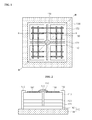
- FIG. 1 is a plan view of a light emitting device according to an embodiment as broadly described herein;
- FIG. 2 is a cross-sectional view taken along line II-II' of the light emitting device shown in FIGs. 1-2 ;
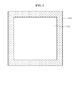
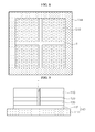
- FIGS. 3 to 17 are process diagrams of a method for manufacturing the light emitting device shown in FIGs. 1-2 ;
- FIGS. 18 and 19 illustrate current spreading characteristics of the light emitting device shown in FIGs. 1-2 .
- a layer when a layer (or film) is referred to as being 'on/over' another layer or substrate, it may be directly on/over another layer or substrate, or intervening layers may be present. Further, when a layer is referred to as being 'under/below' another layer, it may be directly under/below another layer, or one or more intervening layers may be present. In addition, when a layer is referred to as being 'between' two layers, it may be the only layer between the two layers, or one or more intervening layers may also be present.
- Gallium nitride (GaN) semiconductors have high thermal stability and a wide bandgap that may be combined with other elements, such as, for example, In, Al, and the like, making it possible to manufacture a semiconductor layer that emits green light, blue light, and white light while easily controlling emission wavelength.
- the gallium nitride (GaN) semiconductor may be seriously considered in developing a high output electronic device including a light emitting device such as an LED.
- a high current such as, for example, 350mA or more, may be applied to a large area light emitting device.
- Current applied to an N-type electrode pad typically generates current spreading.
- current has straightness at the shortest distance with respect to a P-type electrode, rather than the current spreading described above, causing a current bottleneck phenomenon.
- the current bottleneck phenomenon may cause degradation of an Epi layer, leaving the device vulnerable to radiating characteristics if the device is driven for a long time in a high temperature environment.
- a light emitting device in accordance with the exemplary embodiment shown in FIGs. 1-2 may include a second conductive semiconductor layer 130, an active layer 120, a first conductive semiconductor layer 110, a first insulating layer 150 that separates the first conductive semiconductor layer 110, the active layer 120, and the second conductive semiconductor layer 130 into a plurality of areas, first electrodes 160 that are formed over upper surfaces of the separated first conductive semiconductor layers 110, and a pad electrode 170 that is formed over the first insulating layer 150 to connect the first electrodes 160.
- the second conductive semiconductor layer 130 may be approximately 100 ⁇ 500 nm thick and may be made of materials such as, for example, GaN, InGaN, InAlGaN, AlGaN, InGaAlP, AlGaAs;
- the active layer 120 may be approximately 10 ⁇ 100 nm thick and may be made of materials such as, for example, InGaN/GaN, InGaN/InGaN;
- the first conductive semiconductor layer 110 may be approximately 1000 ⁇ 10000 nm thick and may be made of materials such as, for example, GaN, InGaN, InAlGaN, AlGaN, InGaAlP, AlGaAs;
- the first insulating layer 150 may be made of materials such as, for example, Oxide, Nitride, Polymer film;
- the first electrodes 160 may be approximately 10 ⁇ 5000 nm thick and may be made of materials such as, for example, Cr, Ni, Ti, Al, Ag, Pt, Pd, Au ; and
- an electrode structure that can provide smooth current flow and avoid a current bottleneck phenomenon is needed.
- current applied to an electrode pad formed over an N-type electrode is light-emitted while spreading into a light emitting surface through an N-type electrode.
- the current bottleneck phenomenon is caused.
- the structures may be separated in order to control the current bottleneck phenomenon caused due to the application of high current, making it possible to achieve smooth current spreading.
- a large area light emitting device may be structured so that luminous strength may be relatively uniformly distributed over the area by the smooth current spreading, and may prevent degradation of the Epi layer due to the current bottleneck wile also improving high-temperature reliability.
- the general electrode structure may have a structure in which a wing electrode conforms to a pad electrode. Even in the separated case, since it is a serial type, the current bottleneck phenomenon may occur around the pad electrode when a high current is applied. Since the breakdown current spreading of the Epi layer is not smooth due to the current bottleneck phenomenon caused by the application of high current, the problems discussed above, such as non-uniform emission strength between the light emitting surfaces and the degradation in high temperature reliability during extended operation may still occur.
- the pad electrode 170 may be positioned over the first insulating layer 150 and the first electrodes 160 may be positioned over the light emitting surface.
- current applied to the pad electrode 170 flows to the first electrodes 160 of the light emitting surfaces, which are divided in four quadrants by the pad electrode 170 formed over the first insulating layer 150, then to the pad 170 and the first electrode 160 which contact each other in parallel, as shown in FIGS. 18 and 19 .
- the pad electrode 170 and the first electrode 160 which contact each other in parallel, may have the same current density (C) at each of the four divided light emitting surfaces such that a light emitting surface having a uniform emission strength may be achieved.
- heat generated during extended high temperature operation may be more effectively dissipated, thus improving high temperature reliability and performance characteristics in applications such as BLU, and the like.
- the parallel type electrode structure as embodied and broadly described herein may be focused on the development of an electrode structure for a large area LED display device.
- the parallel type electrode as embodied and broadly described herein may be applied to a vertical type LED as well as a horizontal type LED, and may also be applied to an N-electrode as well as a P-electrode.
- a first substrate 100 may be prepared.
- the first substrate 100 may be a sapphire (Al2O3) single crystal substrate, a SiC substrate, or the like, and is not limited thereto.
- a wet cleaning operation may be performed on the first substrate to remove impurities.
- the first substrate 100 is only shown in FIG. 3A .
- the first conductive semiconductor layer 110 may be formed over, or on, the first substrate 100. This process will be described under the assumption that the first substrate is positioned over the first conductive semiconductor layer 110 based on the orientation shown in the drawings.
- the first conductive semiconductor layer 110 may include an N type GaN layer formed by a Chemical Vapor Deposition (CVD) method, a Molecular Beam Epitaxy (MBE) method, a sputtering, or a Hydride Vapor Phase Epitaxy (HVPE) method, or other method as appropriate. Further, the first conductive semiconductor layer 110 may be formed by implanting silane gas (SiH4) including n type impurities, such as trimethyl gallium gas (TMGa), ammonia gas (NH3), nitrogen gas (N2), silicon (Si), and the like, in a chamber.
- silane gas SiH4
- n type impurities such as trimethyl gallium gas (TMGa), ammonia gas (NH3), nitrogen gas (N2), silicon (Si), and the like
- an undoped semiconductor layer (not shown) may be formed over the first substrate, and the first conductive semiconductor layer 110 may be formed over the undoped semiconductor layer.
- an undoped GaN layer may be formed over the first substrate.
- the active layer 120 may be formed over the first conductive semiconductor layer 110.
- the active layer 120 may be a layer that emits light having energy determined by a unique energy band of an activation (light emitting layer) material by impinging electrons injected through the first conductive semiconductor layer 110 and holes injected through the second conductive semiconductor layer 130.
- the active layer 120 may have a quantum well structure formed by alternately stacking a nitride semiconductor thin film layer having a different energy band one time or several times.
- the active layer 120 may have a multi quantum well structure having an InGaN/GaN structure by implanting trimethyl gallium gas (TMGa), ammonia gas (NH3), nitrogen gas (N2), trimethyl indium gas (TMIn), but is not limited thereto.
- TMGa trimethyl gallium gas
- NH3 ammonia gas
- N2 nitrogen gas
- TIn trimethyl indium gas
- the second conductive semiconductor layer 130 may be formed over the active layer 120.
- the second conductive semiconductor layer 130 may be formed in a P type GaN layer by implanting bicetyl cyclophentadienyl magnesium (EtCp2Mg) ⁇ Mg(C2H5C5H4)2 including p type impurities, such as trimethyl gallium gas (TMGa), ammonia gas (NH3), nitrogen gas (N2), magnesium (Mg), in a chamber, but is not limited thereto.
- TMGa trimethyl gallium gas
- NH3 ammonia gas
- N2 nitrogen gas
- Mg magnesium
- a second electrode layer 140 may be formed over the second conductive semiconductor layer 130.
- the second electrode layer 140 may include an ohmic layer 142 and a second substrate 144.
- the second electrode layer may also include a reflective layer 143 and a coupling layer 145. Simply for ease of illustration, the reflective layer 143 and the coupling layer 145 are only shown in FIG. 3B .
- the second layer 140 may be formed by stacking a single metal, a metal alloy, a metal oxide, and the like, in plurality in order to effectively perform a hole injection.
- the ohmic layer 142 may include at least one of ITO, IZO(In-ZnO), GZO(Ga-ZnO), AZO(Al-ZnO), AGZO(Al-Ga ZnO), IGZO(In-Ga ZnO), IrOx, RuOx, RuOx/ITO, Ni/IrOx/Au, or Ni/IrOx/Au/ITO, but is not limited to thereto.
- the second electrode layer 140 includes a reflective layer
- a reflective layer may be formed of a metal layer including Al, Ag, or an alloy including Al or Ag. These materials effectively reflect light generated from the active layer 120, making it possible to remarkably improve light extraction efficiency of the light emitting device.
- the reflective layer may also act as the coupling layer, or the coupling layer may be formed of nickel (Ni), or gold (Au), and may be provided in addition to or instead of the reflective layer.
- the second layer 140 may include the second substrate 144.
- the second substrate 144 may be formed of a metal having excellent conductivity, a metal alloy, or a conductive semiconductor material.
- the second substrate 144 may be copper (Cu), copper alloy, Si, Mo, SiGe, or the like.
- a method for forming the second substrate 144 may include a electrochemical metal deposition method, a bonding method using an eutectic metal, or other method as appropriate.
- the first substrate may be removed so that the first conductive semiconductor layer 110 is exposed.
- a method for removing the first substrate may include a method of separating the first substrate using high-output laser or a chemical etching method. Further, the first substrate may be removed by being physically ground. Removing the first substrate exposes the first conductive semiconductor layer 110.
- a first pattern 310 may be formed over the first conductive semiconductor layer 110.
- the first pattern 310 may expose an area in which a trench may be formed with a photosensitive film or an insulating film.
- Portions of the first conductive semiconductor layer 110, the active layer 120, the second conductive semiconductor layer 130, and the second electrode layer 140 may be removed along with a process of forming a trench T (see FIG. 7 ). Removal of the outer portions of the first conductive semiconductor layer 110, the active layer 120, the second conductive semiconductor layer 130, and the second electrode layer 140 allow for coupling of a second insulating layer 152 thereto.
- a portion of the outer portion of the ohmic layer 142 in the second electrode layer 140 may also be removed, but the embodiment is not limited thereto.
- the trench T may be formed by dry or wet etching.
- the trench T may be a cross type as shown in FIG. 8 , but is not limited thereto.
- the trench T may separate the LED chip into a plurality of areas in various forms.
- the trench T may be formed by being etched to the second conductive semiconductor layer 130.
- the trench T may also extend into a portion of the second electrode layer 140.
- the first pattern 310 may be removed as shown in FIGS. 9 and 10 .
- the first pattern 310 may be removed by an ashing method, a wet etching method, or other method as appropriate.
- the first insulating layer 150 may be formed as shown in FIGS. 11 and 12 to fill the trench T.
- the first insulating layer 150 may be formed of insulating film such an oxide film or a nitride film.
- FIG. 11 is a cross-sectional view taken along line I-I' of FIG. 12 .
- the second insulating layer 152 surrounding the outer portions of the first conductive semiconductor layer 110, the active layer 120, and the second conductive semiconductor layer 130, may be formed along with the formation of the first insulating layer 150.
- a passivation layer surrounding the outer portions of the first conductive semiconductor layer 110, the active layer 120, the second conductive semiconductor layer 130 may be formed of an insulating film such as an oxide film or a nitride film, etc.
- FIG. 13 is a cross-sectional view taken along line II-II' of FIG. 14 .
- the first electrode 160 contacts the first conductive semiconductor layer 110 over a wide range, but may be formed such that less of the first electrode 160 covers a portion of the first conductive semiconductor layer 110 from which light is emitted.
- the first electrode 160 may be formed as a grid.
- the first electrodes 160 may each be formed over the separated first conductive semiconductor layer 110 in a wing type. Other arrangements may also be appropriate.
- FIGS. 15 , 16, and 17 the pad electrode 170 by which the first electrodes 160 are connected to each other may be formed over the first insulating layer 150.
- FIG. 15 is a cross-sectional view taken along line II-II' of FIG. 16
- FIG. 17 is a cross-sectional view taken along line III-III' of FIG. 16 .
- the parallel type electrode as embodied and broadly described herein, which is a structure in which the pad electrode 170 is disposed over the first insulating layer 150 and the first electrodes 160 are disposed over the light emitting surface
- current applied to the pad electrode 170 flows to the first electrodes 160 of the four divided light emitting surfaces formed over the first insulating layers 150.
- the pad electrode 170 and the first electrodes 160 may contact each other in parallel.
- the pad electrode 170 may be formed at the center of the upper surface of the light emitting structure, such that it may have substantially the same current density (C) at the separated light emitting surface.
- the pad electrode 170 and the first electrode 160 which contact each other in parallel, are distributed to have the same current density (C) at each of the four divided light emitting surfaces such that a light emitting surface having uniform emission strength may be achieved.
- the parallel type electrode structure may solve the current bottleneck phenomenon (crowd phenomenon) as well as provide smooth current spreading.
- the parallel type electrode structure may also provide uniform current density over the light emitting area, and so the activation area may generate uniform emission strength over the entire area by the n-i-p junction, making it possible to obtain improved effect of light amount.
- a light emitting device as embodied and broadly described herein forms an isolation having a wide specific surface area, thereby achieving excellent heat dissipation.
- the isolation having the relatively wider specific surface area may provide improved heat dissipation, thus improving high temperature reliability during extended operation time and improving characteristics in applications such as BLU, etc.
- a light emitting device is provided that is capable of solving a current bottleneck phenomenon, or crowd phenomenon, while smoothly spreading current.
- a light emitting device that has excellent heat dissipating characteristics by forming isolation having a wide specific surface area.
- a light emitting device may comprise a light emitting structure having a second conductive semiconductor layer, an active layer and a first conductive semiconductor layer; and a parallel type electrode structure formed over the light emitting structure.
- the parallel type electrode structure may be provided over the first conductive semiconductor layer.
- a second insulating layer may surround the outer portions of the first conductive semiconductor layer, the active layer, and the second conductive semiconductor layer.
- a first insulating layer may separate the first conductive semiconductor layer, the active layer, the second conductive semiconductor layer into a plurality of areas.
- a first electrodes may be provided over the separated first conductive semiconductor layers. Each first electrode may be separately provided over the separated first conductive semiconductor layer. The first electrode may be provided over the separated first conductive semiconductor layer in a wing type or a grid type.
- a pad may be provided over the first insulating layer.
- the pade may be provided at the center of the light emitting structure to connect the first electrodes.
- the pad may be provided over the first insulating layer and the first electrode is over the light emitting surface.
- the current applied to the pad may flow into the first electrodes of the light emitting surfaces divided in four through the pad electrode over the first insulating layer, the pad and the first electrode contacting each other in parallel.
- the pad and the first electrode, which contact each other in parallel, may have the same current density at the light emitting surfaces divided in four.
- a light emitting device may comprise a light emitting structure that includes a second conductive semiconductor layer, an active layer, and a first conductive semiconductor layer; a first insulating layer that separates the first conductive semiconductor layer, the active layer, the second conductive semiconductor layer into a plurality of areas; a first electrodes over the separated first conductive semiconductor layers; and a pad that is over the first insulating layer to connect the first electrodes.
- the first electrode may be provided over the separated first conductive semiconductor layer in a wing type or a grid type. Each first electrode may be separately provided over the separated first conductive semiconductor layer.
- a portion of the outer portions of a the first conductive semiconductor layer, the active layer, and the second conductive semiconductor layer may be removed.
- a second insulating layer may surround the outer portions of the first conductive semiconductor layer, the active layer, and the second conductive semiconductor layer.
- the pad may be provided at the center of the light emitting structure to connect the first electrodes.
- the current applied to the pad may flow into the first electrodes of the light emitting surfaces divided in four through the pad electrode over the first insulating layer, the pad and the first electrode contacting each other in parallel.
- the pad and the first electrode, which contact each other in parallel, may have the same current density at the light emitting surfaces divided in four.
- any reference in this specification to "one embodiment,” “an embodiment,” “example embodiment,” etc. means that a particular feature, structure, or characteristic described in connection with the embodiment is included in at least one embodiment of the invention.
- the appearances of such phrases in various places in the specification are not necessarily all referring to the same embodiment.
Landscapes
- Led Devices (AREA)
Abstract
Description
- Embodiments as broadly described herein relate to a light emitting device.
- A light emitting device is a semiconductor device that converts current into light. A red light emitting device may be used as a light source for electronic devices, information telecommunication devices, and the like, together with a green light emitting device. One example of such light emitting devices is a light emitting diode (LED). Due to widespread use of such devices, improvements in reliability and performance of such devices is desirable.
- The embodiments will be described in detail with reference to the following drawings in which like reference numerals refer to like elements wherein:
-
FIG. 1 is a plan view of a light emitting device according to an embodiment as broadly described herein; -
FIG. 2 is a cross-sectional view taken along line II-II' of the light emitting device shown inFIGs. 1-2 ; -
FIGS. 3 to 17 are process diagrams of a method for manufacturing the light emitting device shown inFIGs. 1-2 ; and -
FIGS. 18 and 19 illustrate current spreading characteristics of the light emitting device shown inFIGs. 1-2 . - Hereinafter, a light emitting device according to embodiments as broadly described herein will be discussed with reference to the accompanying drawings.
- In the description of embodiments, when a layer (or film) is referred to as being 'on/over' another layer or substrate, it may be directly on/over another layer or substrate, or intervening layers may be present. Further, when a layer is referred to as being 'under/below' another layer, it may be directly under/below another layer, or one or more intervening layers may be present. In addition, when a layer is referred to as being 'between' two layers, it may be the only layer between the two layers, or one or more intervening layers may also be present.
- Gallium nitride (GaN) semiconductors have high thermal stability and a wide bandgap that may be combined with other elements, such as, for example, In, Al, and the like, making it possible to manufacture a semiconductor layer that emits green light, blue light, and white light while easily controlling emission wavelength. As a result, the gallium nitride (GaN) semiconductor may be seriously considered in developing a high output electronic device including a light emitting device such as an LED.
- A high current, such as, for example, 350mA or more, may be applied to a large area light emitting device. Current applied to an N-type electrode pad typically generates current spreading. However, when a high current is applied, current has straightness at the shortest distance with respect to a P-type electrode, rather than the current spreading described above, causing a current bottleneck phenomenon. The current bottleneck phenomenon may cause degradation of an Epi layer, leaving the device vulnerable to radiating characteristics if the device is driven for a long time in a high temperature environment.
- A light emitting device in accordance with the exemplary embodiment shown in
FIGs. 1-2 may include a secondconductive semiconductor layer 130, anactive layer 120, a firstconductive semiconductor layer 110, a firstinsulating layer 150 that separates the firstconductive semiconductor layer 110, theactive layer 120, and the secondconductive semiconductor layer 130 into a plurality of areas,first electrodes 160 that are formed over upper surfaces of the separated firstconductive semiconductor layers 110, and apad electrode 170 that is formed over the firstinsulating layer 150 to connect thefirst electrodes 160. - In certain embodiments, the second
conductive semiconductor layer 130 may be approximately 100∼500 nm thick and may be made of materials such as, for example, GaN, InGaN, InAlGaN, AlGaN, InGaAlP, AlGaAs; theactive layer 120 may be approximately 10∼100 nm thick and may be made of materials such as, for example, InGaN/GaN, InGaN/InGaN; the firstconductive semiconductor layer 110 may be approximately 1000∼10000 nm thick and may be made of materials such as, for example, GaN, InGaN, InAlGaN, AlGaN, InGaAlP, AlGaAs; thefirst insulating layer 150 may be made of materials such as, for example, Oxide, Nitride, Polymer film; thefirst electrodes 160 may be approximately 10∼5000 nm thick and may be made of materials such as, for example, Cr, Ni, Ti, Al, Ag, Pt, Pd, Au ; and thepad electrode 170 may be approximately 100∼5000 nm thick and may be made of materials such as, for example, Cr, Ni, Ti, Al, Ag, Pt, Pd, Au . Other combinations of thickenesses and/or materials may also be appropriate. - As discussed above, in manufacturing a large area light emitting device, an electrode structure that can provide smooth current flow and avoid a current bottleneck phenomenon is needed. However, in the case of a vertical type GaN light emitting device, current applied to an electrode pad formed over an N-type electrode is light-emitted while spreading into a light emitting surface through an N-type electrode. As discussed above, in the case of the large area light emitting device, when a high current is applied, the current bottleneck phenomenon is caused.
- In an embodiment in which parallel type electrode structures are formed over GaN LEDs, the structures may be separated in order to control the current bottleneck phenomenon caused due to the application of high current, making it possible to achieve smooth current spreading. Such a large area light emitting device may be structured so that luminous strength may be relatively uniformly distributed over the area by the smooth current spreading, and may prevent degradation of the Epi layer due to the current bottleneck wile also improving high-temperature reliability.
- The general electrode structure may have a structure in which a wing electrode conforms to a pad electrode. Even in the separated case, since it is a serial type, the current bottleneck phenomenon may occur around the pad electrode when a high current is applied. Since the breakdown current spreading of the Epi layer is not smooth due to the current bottleneck phenomenon caused by the application of high current, the problems discussed above, such as non-uniform emission strength between the light emitting surfaces and the degradation in high temperature reliability during extended operation may still occur.
- In a parallel type electrode structure in accordance with an embodiment as broadly described herein, the
pad electrode 170 may be positioned over the firstinsulating layer 150 and thefirst electrodes 160 may be positioned over the light emitting surface. In this structure current applied to thepad electrode 170 flows to thefirst electrodes 160 of the light emitting surfaces, which are divided in four quadrants by thepad electrode 170 formed over the firstinsulating layer 150, then to thepad 170 and thefirst electrode 160 which contact each other in parallel, as shown inFIGS. 18 and 19 . - The
pad electrode 170 and thefirst electrode 160, which contact each other in parallel, may have the same current density (C) at each of the four divided light emitting surfaces such that a light emitting surface having a uniform emission strength may be achieved. - In addition, by isolating the relatively wider specific surface area, heat generated during extended high temperature operation may be more effectively dissipated, thus improving high temperature reliability and performance characteristics in applications such as BLU, and the like.
- As the area of the light emitting device such as an LED is increased, driving the LED with a high current application scheme may benefit from improvement of the electrode structure. Therefore, the parallel type electrode structure as embodied and broadly described herein may be focused on the development of an electrode structure for a large area LED display device. The parallel type electrode as embodied and broadly described herein may be applied to a vertical type LED as well as a horizontal type LED, and may also be applied to an N-electrode as well as a P-electrode.
- Hereinafter, a method for manufacturing a light emitting device according to an embodiment as broadly described herein will be discussed with reference to
FIGS. 3 to 17 . - First, a first substrate 100 may be prepared. The first substrate 100 may be a sapphire (Al2O3) single crystal substrate, a SiC substrate, or the like, and is not limited thereto. A wet cleaning operation may be performed on the first substrate to remove impurities. Simply for ease of illustration, the first substrate 100 is only shown in
FIG. 3A . Thereafter, the firstconductive semiconductor layer 110 may be formed over, or on, the first substrate 100. This process will be described under the assumption that the first substrate is positioned over the firstconductive semiconductor layer 110 based on the orientation shown in the drawings. - The first
conductive semiconductor layer 110 may include an N type GaN layer formed by a Chemical Vapor Deposition (CVD) method, a Molecular Beam Epitaxy (MBE) method, a sputtering, or a Hydride Vapor Phase Epitaxy (HVPE) method, or other method as appropriate. Further, the firstconductive semiconductor layer 110 may be formed by implanting silane gas (SiH4) including n type impurities, such as trimethyl gallium gas (TMGa), ammonia gas (NH3), nitrogen gas (N2), silicon (Si), and the like, in a chamber. - In alterative embodiments, an undoped semiconductor layer (not shown) may be formed over the first substrate, and the first
conductive semiconductor layer 110 may be formed over the undoped semiconductor layer. For example, an undoped GaN layer may be formed over the first substrate. - After the first
conductive semiconductor layer 110 is formed over the first substrate, theactive layer 120 may be formed over the firstconductive semiconductor layer 110. Theactive layer 120 may be a layer that emits light having energy determined by a unique energy band of an activation (light emitting layer) material by impinging electrons injected through the firstconductive semiconductor layer 110 and holes injected through the secondconductive semiconductor layer 130. Theactive layer 120 may have a quantum well structure formed by alternately stacking a nitride semiconductor thin film layer having a different energy band one time or several times. For example, theactive layer 120 may have a multi quantum well structure having an InGaN/GaN structure by implanting trimethyl gallium gas (TMGa), ammonia gas (NH3), nitrogen gas (N2), trimethyl indium gas (TMIn), but is not limited thereto. - Thereafter, the second
conductive semiconductor layer 130 may be formed over theactive layer 120. For example, the secondconductive semiconductor layer 130 may be formed in a P type GaN layer by implanting bicetyl cyclophentadienyl magnesium (EtCp2Mg) {Mg(C2H5C5H4)2 including p type impurities, such as trimethyl gallium gas (TMGa), ammonia gas (NH3), nitrogen gas (N2), magnesium (Mg), in a chamber, but is not limited thereto. - Next, a
second electrode layer 140 may be formed over the secondconductive semiconductor layer 130. Thesecond electrode layer 140 may include anohmic layer 142 and asecond substrate 144. The second electrode layer may also include a reflective layer 143 and acoupling layer 145. Simply for ease of illustration, the reflective layer 143 and thecoupling layer 145 are only shown inFIG. 3B . - The
second layer 140 may be formed by stacking a single metal, a metal alloy, a metal oxide, and the like, in plurality in order to effectively perform a hole injection. For example, theohmic layer 142 may include at least one of ITO, IZO(In-ZnO), GZO(Ga-ZnO), AZO(Al-ZnO), AGZO(Al-Ga ZnO), IGZO(In-Ga ZnO), IrOx, RuOx, RuOx/ITO, Ni/IrOx/Au, or Ni/IrOx/Au/ITO, but is not limited to thereto. - When the
second electrode layer 140 includes a reflective layer, such a reflective layer may be formed of a metal layer including Al, Ag, or an alloy including Al or Ag. These materials effectively reflect light generated from theactive layer 120, making it possible to remarkably improve light extraction efficiency of the light emitting device. - Further, when the
second electrode layer 140 includes a coupling layer, the reflective layer may also act as the coupling layer, or the coupling layer may be formed of nickel (Ni), or gold (Au), and may be provided in addition to or instead of the reflective layer. - The
second layer 140 may include thesecond substrate 144. When the firstconductive semiconductor layer 110 has a sufficient thickness of 50 or more, a process of forming thesecond substrate 144 may be omitted. In order to effectively inject holes, thesecond substrate 144 may be formed of a metal having excellent conductivity, a metal alloy, or a conductive semiconductor material. For example, thesecond substrate 144 may be copper (Cu), copper alloy, Si, Mo, SiGe, or the like. A method for forming thesecond substrate 144 may include a electrochemical metal deposition method, a bonding method using an eutectic metal, or other method as appropriate. - Thereafter, the first substrate may be removed so that the first
conductive semiconductor layer 110 is exposed. A method for removing the first substrate may include a method of separating the first substrate using high-output laser or a chemical etching method. Further, the first substrate may be removed by being physically ground. Removing the first substrate exposes the firstconductive semiconductor layer 110. - Hereinafter, a process of forming the first insulating
layer 150 will be described with reference toFIGS. 5 to 12 . - As shown in
FIGS. 5 and 6 , afirst pattern 310 may be formed over the firstconductive semiconductor layer 110. For example, thefirst pattern 310 may expose an area in which a trench may be formed with a photosensitive film or an insulating film. Portions of the firstconductive semiconductor layer 110, theactive layer 120, the secondconductive semiconductor layer 130, and thesecond electrode layer 140 may be removed along with a process of forming a trench T (seeFIG. 7 ). Removal of the outer portions of the firstconductive semiconductor layer 110, theactive layer 120, the secondconductive semiconductor layer 130, and thesecond electrode layer 140 allow for coupling of a second insulatinglayer 152 thereto. As shown inFIG. 3A , a portion of the outer portion of theohmic layer 142 in thesecond electrode layer 140 may also be removed, but the embodiment is not limited thereto. - Next, as shown in
FIGS. 7 and8 , a portion of the firstconductive semiconductor layer 110, theactive layer 120, and the secondconductive semiconductor layer 130 may be etched using thefirst pattern 310 as an etch mask to form the trench T. For example, the trench T may be formed by dry or wet etching. The trench T may be a cross type as shown inFIG. 8 , but is not limited thereto. The trench T may separate the LED chip into a plurality of areas in various forms. In this embodiment, the trench T may be formed by being etched to the secondconductive semiconductor layer 130. In certain embodiments, the trench T may also extend into a portion of thesecond electrode layer 140. - Subsequently, the
first pattern 310 may be removed as shown inFIGS. 9 and10 . For example, thefirst pattern 310 may be removed by an ashing method, a wet etching method, or other method as appropriate. - Next, the first insulating
layer 150 may be formed as shown inFIGS. 11 and12 to fill the trench T. For example, the first insulatinglayer 150 may be formed of insulating film such an oxide film or a nitride film.FIG. 11 is a cross-sectional view taken along line I-I' ofFIG. 12 . - The second
insulating layer 152 surrounding the outer portions of the firstconductive semiconductor layer 110, theactive layer 120, and the secondconductive semiconductor layer 130, may be formed along with the formation of the first insulatinglayer 150. For example, a passivation layer surrounding the outer portions of the firstconductive semiconductor layer 110, theactive layer 120, the secondconductive semiconductor layer 130 may be formed of an insulating film such as an oxide film or a nitride film, etc. - Next, as shown in
FIGS. 13 and14 , thefirst electrodes 160 may each be formed over the separated firstconductive semiconductor layer 110.FIG. 13 is a cross-sectional view taken along line II-II' ofFIG. 14 . - In this embodiment, the
first electrode 160 contacts the firstconductive semiconductor layer 110 over a wide range, but may be formed such that less of thefirst electrode 160 covers a portion of the firstconductive semiconductor layer 110 from which light is emitted. For example, thefirst electrode 160 may be formed as a grid. Alternatively, thefirst electrodes 160 may each be formed over the separated firstconductive semiconductor layer 110 in a wing type. Other arrangements may also be appropriate. - Subsequently, as shown in
FIGS. 15 ,16, and 17 , thepad electrode 170 by which thefirst electrodes 160 are connected to each other may be formed over the first insulatinglayer 150.FIG. 15 is a cross-sectional view taken along line II-II' ofFIG. 16 and FIG. 17 is a cross-sectional view taken along line III-III' ofFIG. 16 . - As shown in
FIGS. 18 and 19 , in the parallel type electrode as embodied and broadly described herein, which is a structure in which thepad electrode 170 is disposed over the first insulatinglayer 150 and thefirst electrodes 160 are disposed over the light emitting surface, current applied to thepad electrode 170 flows to thefirst electrodes 160 of the four divided light emitting surfaces formed over the first insulatinglayers 150. Thepad electrode 170 and thefirst electrodes 160 may contact each other in parallel. In this embodiment, thepad electrode 170 may be formed at the center of the upper surface of the light emitting structure, such that it may have substantially the same current density (C) at the separated light emitting surface. - Therefore, the
pad electrode 170 and thefirst electrode 160, which contact each other in parallel, are distributed to have the same current density (C) at each of the four divided light emitting surfaces such that a light emitting surface having uniform emission strength may be achieved. - In a light emitting device as embodied and broadly described herein, the parallel type electrode structure may solve the current bottleneck phenomenon (crowd phenomenon) as well as provide smooth current spreading.
- The parallel type electrode structure may also provide uniform current density over the light emitting area, and so the activation area may generate uniform emission strength over the entire area by the n-i-p junction, making it possible to obtain improved effect of light amount.
- Further, a light emitting device as embodied and broadly described herein forms an isolation having a wide specific surface area, thereby achieving excellent heat dissipation. In addition, the isolation having the relatively wider specific surface area may provide improved heat dissipation, thus improving high temperature reliability during extended operation time and improving characteristics in applications such as BLU, etc.
- A light emitting device is provided that is capable of solving a current bottleneck phenomenon, or crowd phenomenon, while smoothly spreading current.
- A light emitting device is provided that has excellent heat dissipating characteristics by forming isolation having a wide specific surface area.
- As described above, a light emitting device may comprise a light emitting structure having a second conductive semiconductor layer, an active layer and a first conductive semiconductor layer; and a parallel type electrode structure formed over the light emitting structure. The parallel type electrode structure may be provided over the first conductive semiconductor layer. A second insulating layer may surround the outer portions of the first conductive semiconductor layer, the active layer, and the second conductive semiconductor layer.
- A first insulating layer may separate the first conductive semiconductor layer, the active layer, the second conductive semiconductor layer into a plurality of areas. A first electrodes may be provided over the separated first conductive semiconductor layers. Each first electrode may be separately provided over the separated first conductive semiconductor layer. The first electrode may be provided over the separated first conductive semiconductor layer in a wing type or a grid type.
- A pad may be provided over the first insulating layer. The pade may be provided at the center of the light emitting structure to connect the first electrodes. The pad may be provided over the first insulating layer and the first electrode is over the light emitting surface. The current applied to the pad may flow into the first electrodes of the light emitting surfaces divided in four through the pad electrode over the first insulating layer, the pad and the first electrode contacting each other in parallel. The pad and the first electrode, which contact each other in parallel, may have the same current density at the light emitting surfaces divided in four.
- Further, a light emitting device may comprise a light emitting structure that includes a second conductive semiconductor layer, an active layer, and a first conductive semiconductor layer; a first insulating layer that separates the first conductive semiconductor layer, the active layer, the second conductive semiconductor layer into a plurality of areas; a first electrodes over the separated first conductive semiconductor layers; and a pad that is over the first insulating layer to connect the first electrodes.
- The first electrode may be provided over the separated first conductive semiconductor layer in a wing type or a grid type. Each first electrode may be separately provided over the separated first conductive semiconductor layer.
- A portion of the outer portions of a the first conductive semiconductor layer, the active layer, and the second conductive semiconductor layer may be removed. A second insulating layer may surround the outer portions of the first conductive semiconductor layer, the active layer, and the second conductive semiconductor layer.
The pad may be provided at the center of the light emitting structure to connect the first electrodes. The current applied to the pad may flow into the first electrodes of the light emitting surfaces divided in four through the pad electrode over the first insulating layer, the pad and the first electrode contacting each other in parallel. The pad and the first electrode, which contact each other in parallel, may have the same current density at the light emitting surfaces divided in four. - Any reference in this specification to "one embodiment," "an embodiment," "example embodiment," etc., means that a particular feature, structure, or characteristic described in connection with the embodiment is included in at least one embodiment of the invention. The appearances of such phrases in various places in the specification are not necessarily all referring to the same embodiment. Further, when a particular feature, structure, or characteristic is described in connection with any embodiment, it is submitted that it is within the purview of one skilled in the art to effect such feature, structure, or characteristic in connection with other ones of the embodiments.
- Although embodiments have been described with reference to a number of illustrative embodiments thereof, it should be understood that numerous other modifications and embodiments can be devised by those skilled in the art that will fall within the spirit and scope of the principles of this disclosure. More particularly, numerous variations and modifications are possible in the component parts and/or arrangements of the subject combination arrangement within the scope of the disclosure, the drawings and the appended claims. In addition to variations and modifications in the component parts and/or arrangements, alternative uses will also be apparent to those skilled in the art.
Claims (15)
- A light emitting device, comprising:a plurality of light emitting elements formed on a first common electrode, each light emitting element having a first conductive layer formed over the first common electrode, an active layer formed over the first conductive layer and a second conductive layer formed over the active layer;at least one insulator formed between adjacent light emitting elements;a corresponding plurality of electrodes respectively formed on the plurality of light emtting elments; anda second common electrode that couples the plurality electrodes.
- The light emitting device of claim 1, wherein the second common electrode is formed over the at least one insulator.
- The light emitting device of claim 1, wherein each electrode of the plurality of electrodes is formed on a corresponding portion of the second conductive layer of the light emitting element.
- The light emitting device of claim 1, wherein the plurality of light emitting elements are substantially co-planar on the first common electrode.
- The light emitting device of claim 1, wherein adjacent light emitting elements of the plurality of light emitting elements are separated by a trench, and the at least one insulator is formed in the the trench.
- The light emitting device according to claim 1, wherein the second common electrode is located substantially at a center of the plurality of light emitting elements.
- The light emitting device of claim 1, wherein current flows from the second common electrode to each of the plurality of electrodes using a separate current path..
- The light emitting device of claim 1, wherein the electrodes of adjacent light emitting elements are formed to be complementary in shape.
- The light emitting device of claim 1, wherein the at least one insulator comprises:a first insulator positioned between adjacent light emitting elements; anda second insulator that surrounds outer peripheral portions of the first conductive layer, the active layer, and the second conductive layer.
- A method of making a light emitting element, the method comprising:forming a first conductive layer;forming an active layer;forming a second conductive layer;providing a first common electrode on the second conductive layer;forming at least one trench through the first conductive layer and the active layer to form a plurality of light emitting elements;respectively forming a plurality of electrodes on the plurality of light emitting elements; andforming a second common electrode to couple the plurality of electrodes.
- The method of claim 10, further comprising:providing a first insulator in the at least one trench so as to isolate the plurality of light emitting elements; andproviding a second insulator surrounding an outer peripheral portion of the first conductive layer, the active layer and the second conductive layer.
- The method of claim 10, wherein respectively forming a plurality of electrodes on the plurality of light emitting elements comprises forming an electrode on each of the plurlaity of electrodes defined by the at least one trench in a grid type arrangement.
- The method of claim 10, wherein providing a first common electrode on the second conductive layer comprises:providing an ohmic layer on the second conductive layer; andproviding a substrate on a side of the ohmic layer opposite the second conductive layer.
- The method of claim 13, wherein forming at least one trench through the first conductive layer and the active layer further comprises extending the at least one trench through the second conductive layer and into the ohmic layer.
- The method of claim 13, wherein forming at least one trench through the first conductive layer and the active layer further comprises extending the at least one trench into the second conductive layer.
Applications Claiming Priority (1)
| Application Number | Priority Date | Filing Date | Title |
|---|---|---|---|
| KR1020090013572A KR101007130B1 (en) | 2009-02-18 | 2009-02-18 | Light emitting device and manufacturing method |
Publications (2)
| Publication Number | Publication Date |
|---|---|
| EP2221873A1 true EP2221873A1 (en) | 2010-08-25 |
| EP2221873B1 EP2221873B1 (en) | 2020-04-08 |
Family
ID=42237287
Family Applications (1)
| Application Number | Title | Priority Date | Filing Date |
|---|---|---|---|
| EP10150474.4A Active EP2221873B1 (en) | 2009-02-18 | 2010-01-12 | Light emitting device |
Country Status (5)
| Country | Link |
|---|---|
| US (1) | US8242509B2 (en) |
| EP (1) | EP2221873B1 (en) |
| KR (1) | KR101007130B1 (en) |
| CN (1) | CN101807593B (en) |
| WO (1) | WO2010095781A1 (en) |
Families Citing this family (24)
| Publication number | Priority date | Publication date | Assignee | Title |
|---|---|---|---|---|
| US8148733B2 (en) * | 2007-06-12 | 2012-04-03 | SemiLEDs Optoelectronics Co., Ltd. | Vertical LED with current guiding structure |
| JP5336594B2 (en) * | 2009-06-15 | 2013-11-06 | パナソニック株式会社 | Semiconductor light emitting device, light emitting module, and lighting device |
| CN102468318B (en) * | 2010-11-04 | 2014-12-24 | 上海蓝光科技有限公司 | Chip structure of high-voltage direct current light emitting diode and method for manufacturing chip structure |
| WO2012164437A2 (en) * | 2011-06-01 | 2012-12-06 | Koninklijke Philips Electronics N.V. | Light emitting device bonded to a support substrate |
| JP5629669B2 (en) * | 2011-10-11 | 2014-11-26 | 株式会社東芝 | Manufacturing method of semiconductor light emitting device |
| US9847372B2 (en) * | 2011-12-01 | 2017-12-19 | Micron Technology, Inc. | Solid state transducer devices with separately controlled regions, and associated systems and methods |
| TWI618267B (en) * | 2013-03-18 | 2018-03-11 | 晶元光電股份有限公司 | Light-emitting element |
| FR3011383B1 (en) * | 2013-09-30 | 2017-05-26 | Commissariat Energie Atomique | METHOD FOR MANUFACTURING OPTOELECTRONIC DEVICES WITH ELECTROLUMINESCENT DIODES |
| KR20150064414A (en) * | 2013-12-03 | 2015-06-11 | 삼성전자주식회사 | Light emitting device and lighting appratus having the same |
| CN103972350B (en) * | 2014-05-30 | 2017-01-18 | 马鞍山太时芯光科技有限公司 | LED (light-emitting diode) chip with novel structure and production method thereof |
| KR20150139194A (en) * | 2014-06-03 | 2015-12-11 | 서울바이오시스 주식회사 | Light emitting diode and method of fabricating the same |
| US9728698B2 (en) | 2014-06-03 | 2017-08-08 | Seoul Viosys Co., Ltd. | Light emitting device package having improved heat dissipation efficiency |
| US9577171B2 (en) | 2014-06-03 | 2017-02-21 | Seoul Viosys Co., Ltd. | Light emitting device package having improved heat dissipation efficiency |
| CN111599832B (en) * | 2014-06-23 | 2023-03-24 | 晶元光电股份有限公司 | Photoelectric element and manufacturing method thereof |
| KR102226455B1 (en) * | 2014-07-01 | 2021-03-11 | 엘지전자 주식회사 | Manufacturing method for semiconductor light emitting device |
| JP6312552B2 (en) * | 2014-08-07 | 2018-04-18 | シャープ株式会社 | Semiconductor light emitting device manufacturing method and semiconductor light emitting device |
| CN110690249B (en) * | 2015-02-13 | 2024-01-19 | 首尔伟傲世有限公司 | Light emitting element |
| TWI626771B (en) * | 2016-07-26 | 2018-06-11 | 宏齊科技股份有限公司 | Light emitting diode unit and slim planar light source module |
| WO2018031027A1 (en) * | 2016-08-12 | 2018-02-15 | Intel Corporation | Quantum dot array devices |
| FR3061360A1 (en) * | 2016-12-22 | 2018-06-29 | Commissariat A L'energie Atomique Et Aux Energies Alternatives | LIGHT EMITTING DEVICE |
| KR102446211B1 (en) * | 2017-12-11 | 2022-09-23 | 삼성디스플레이 주식회사 | Light-emitting element inspection method and light-emitting element inspection apparatus |
| KR20220077207A (en) * | 2020-11-30 | 2022-06-09 | 삼성디스플레이 주식회사 | Display device and method for manufacturing of the same |
| KR102831120B1 (en) * | 2021-02-03 | 2025-07-04 | 삼성전자주식회사 | Light emitting device and display apparatus including the same |
| EP4040495A1 (en) * | 2021-02-03 | 2022-08-10 | Samsung Electronics Co., Ltd. | Light-emitting device and display apparatus including the same |
Citations (6)
| Publication number | Priority date | Publication date | Assignee | Title |
|---|---|---|---|---|
| EP0011418A1 (en) * | 1978-11-20 | 1980-05-28 | THE GENERAL ELECTRIC COMPANY, p.l.c. | Manufacture of electroluminescent display devices |
| US5499124A (en) * | 1990-12-31 | 1996-03-12 | Vu; Duy-Phach | Polysilicon transistors formed on an insulation layer which is adjacent to a liquid crystal material |
| WO2003017320A1 (en) * | 2001-08-21 | 2003-02-27 | Nam-Young Kim | Lamp utilizing a light emitted diode |
| US20070007584A1 (en) * | 2005-07-06 | 2007-01-11 | Samsung Electro-Mechanics Co., Ltd. | Nitride semiconductor light emitting diode and method of manufacturing the same |
| US20070215881A1 (en) * | 2006-03-03 | 2007-09-20 | Semiconductor Energy Laboratory Co., Ltd. | Light-emitting element and manufacturing method thereof |
| US20080179602A1 (en) * | 2007-01-22 | 2008-07-31 | Led Lighting Fixtures, Inc. | Fault tolerant light emitters, systems incorporating fault tolerant light emitters and methods of fabricating fault tolerant light emitters |
Family Cites Families (9)
| Publication number | Priority date | Publication date | Assignee | Title |
|---|---|---|---|---|
| JP4902040B2 (en) * | 2000-06-21 | 2012-03-21 | 日亜化学工業株式会社 | Nitride semiconductor device |
| US6547249B2 (en) | 2001-03-29 | 2003-04-15 | Lumileds Lighting U.S., Llc | Monolithic series/parallel led arrays formed on highly resistive substrates |
| KR100495004B1 (en) * | 2002-07-09 | 2005-06-10 | 엘지이노텍 주식회사 | Light emitting diode and method for fabricating thereof |
| JP4703236B2 (en) * | 2005-03-31 | 2011-06-15 | 三洋電機株式会社 | Light emitting device and manufacturing method thereof |
| KR20070088145A (en) | 2006-02-24 | 2007-08-29 | 엘지전자 주식회사 | Light emitting diodes and manufacturing method |
| KR100752721B1 (en) | 2006-07-12 | 2007-08-29 | 삼성전기주식회사 | Method for manufacturing vertical structure gallium nitride based LED device |
| CN100544014C (en) | 2006-09-13 | 2009-09-23 | 海立尔股份有限公司 | LED structure |
| CN102683376A (en) | 2007-01-22 | 2012-09-19 | 科锐公司 | High-pressure light emitter, light emitter and illumination device |
| KR100845549B1 (en) | 2007-01-22 | 2008-07-10 | 삼성전기주식회사 | White light emitting device and its manufacturing method |
-
2009
- 2009-02-18 KR KR1020090013572A patent/KR101007130B1/en not_active Expired - Fee Related
- 2009-05-21 WO PCT/KR2009/002689 patent/WO2010095781A1/en not_active Ceased
-
2010
- 2010-01-12 EP EP10150474.4A patent/EP2221873B1/en active Active
- 2010-02-03 CN CN2010101103986A patent/CN101807593B/en not_active Expired - Fee Related
- 2010-02-04 US US12/699,991 patent/US8242509B2/en not_active Expired - Fee Related
Patent Citations (6)
| Publication number | Priority date | Publication date | Assignee | Title |
|---|---|---|---|---|
| EP0011418A1 (en) * | 1978-11-20 | 1980-05-28 | THE GENERAL ELECTRIC COMPANY, p.l.c. | Manufacture of electroluminescent display devices |
| US5499124A (en) * | 1990-12-31 | 1996-03-12 | Vu; Duy-Phach | Polysilicon transistors formed on an insulation layer which is adjacent to a liquid crystal material |
| WO2003017320A1 (en) * | 2001-08-21 | 2003-02-27 | Nam-Young Kim | Lamp utilizing a light emitted diode |
| US20070007584A1 (en) * | 2005-07-06 | 2007-01-11 | Samsung Electro-Mechanics Co., Ltd. | Nitride semiconductor light emitting diode and method of manufacturing the same |
| US20070215881A1 (en) * | 2006-03-03 | 2007-09-20 | Semiconductor Energy Laboratory Co., Ltd. | Light-emitting element and manufacturing method thereof |
| US20080179602A1 (en) * | 2007-01-22 | 2008-07-31 | Led Lighting Fixtures, Inc. | Fault tolerant light emitters, systems incorporating fault tolerant light emitters and methods of fabricating fault tolerant light emitters |
Also Published As
| Publication number | Publication date |
|---|---|
| WO2010095781A1 (en) | 2010-08-26 |
| KR20100094243A (en) | 2010-08-26 |
| US8242509B2 (en) | 2012-08-14 |
| EP2221873B1 (en) | 2020-04-08 |
| CN101807593B (en) | 2012-11-14 |
| US20100207123A1 (en) | 2010-08-19 |
| CN101807593A (en) | 2010-08-18 |
| KR101007130B1 (en) | 2011-01-10 |
Similar Documents
| Publication | Publication Date | Title |
|---|---|---|
| US8242509B2 (en) | Light emitting device | |
| KR101064053B1 (en) | Light emitting device and manufacturing method | |
| US8680560B2 (en) | LED and LED package | |
| KR101007139B1 (en) | Light emitting device and manufacturing method | |
| US20130037841A1 (en) | Semiconductor light emitting device | |
| KR100986440B1 (en) | Light emitting device and method for fabricating the same | |
| KR101154750B1 (en) | Light emitting device and method for fabricating the same | |
| CN112750931B (en) | Micro light-emitting diode, micro light-emitting diode array substrate and manufacturing method thereof | |
| KR100999756B1 (en) | Light emitting device and manufacturing method | |
| EP2251916A1 (en) | Light emitting device, light emitting device package and lighting system including the same | |
| KR101114047B1 (en) | Light emitting device and method for fabricating the same | |
| CN102623481A (en) | Light emitting device and fabricating method thereof | |
| KR20110043282A (en) | Light emitting device and manufacturing method | |
| CN111052409A (en) | Light Emitting Diode Device and Method of Manufacturing Light Emitting Diode Device | |
| KR101007145B1 (en) | Method of manufacturing light emitting device chip, light emitting device package and light emitting device chip | |
| EP2221886B1 (en) | Semiconductor light-emitting device | |
| KR20160145413A (en) | Red light emitting device and method for fabricating the same, and light emitting device package | |
| KR102561565B1 (en) | Light emitting device and light emitting device package | |
| KR101172136B1 (en) | Light emitting device, method for fabricating the same and light emitting device package | |
| KR102299735B1 (en) | Light emitting device and lighting system | |
| KR102261950B1 (en) | Light emitting device and lighting system | |
| KR102342718B1 (en) | Red light emitting device and lighting system | |
| KR101633814B1 (en) | light emitting device | |
| KR101550951B1 (en) | Light emitting device | |
| KR20170064296A (en) | Light emitting device and lighting apparatus |
Legal Events
| Date | Code | Title | Description |
|---|---|---|---|
| PUAI | Public reference made under article 153(3) epc to a published international application that has entered the european phase |
Free format text: ORIGINAL CODE: 0009012 |
|
| AK | Designated contracting states |
Kind code of ref document: A1 Designated state(s): AT BE BG CH CY CZ DE DK EE ES FI FR GB GR HR HU IE IS IT LI LT LU LV MC MK MT NL NO PL PT RO SE SI SK SM TR |
|
| AX | Request for extension of the european patent |
Extension state: AL BA RS |
|
| RAP1 | Party data changed (applicant data changed or rights of an application transferred) |
Owner name: LG INNOTEK CO., LTD. |
|
| 17P | Request for examination filed |
Effective date: 20110225 |
|
| RAP1 | Party data changed (applicant data changed or rights of an application transferred) |
Owner name: LG INNOTEK CO., LTD. |
|
| RAP1 | Party data changed (applicant data changed or rights of an application transferred) |
Owner name: LG INNOTEK CO., LTD. |
|
| STAA | Information on the status of an ep patent application or granted ep patent |
Free format text: STATUS: EXAMINATION IS IN PROGRESS |
|
| 17Q | First examination report despatched |
Effective date: 20171116 |
|
| RIC1 | Information provided on ipc code assigned before grant |
Ipc: H01L 33/08 20100101AFI20190814BHEP Ipc: H01L 33/38 20100101ALI20190814BHEP Ipc: H01L 27/15 20060101ALN20190814BHEP |
|
| GRAP | Despatch of communication of intention to grant a patent |
Free format text: ORIGINAL CODE: EPIDOSNIGR1 |
|
| STAA | Information on the status of an ep patent application or granted ep patent |
Free format text: STATUS: GRANT OF PATENT IS INTENDED |
|
| RIC1 | Information provided on ipc code assigned before grant |
Ipc: H01L 27/15 20060101ALN20190913BHEP Ipc: H01L 33/38 20100101ALI20190913BHEP Ipc: H01L 33/08 20100101AFI20190913BHEP |
|
| INTG | Intention to grant announced |
Effective date: 20191004 |
|
| RIN1 | Information on inventor provided before grant (corrected) |
Inventor name: HYUN, DON SONG |
|
| GRAJ | Information related to disapproval of communication of intention to grant by the applicant or resumption of examination proceedings by the epo deleted |
Free format text: ORIGINAL CODE: EPIDOSDIGR1 |
|
| STAA | Information on the status of an ep patent application or granted ep patent |
Free format text: STATUS: EXAMINATION IS IN PROGRESS |
|
| REG | Reference to a national code |
Ref country code: DE Ref legal event code: R079 Ref document number: 602010063796 Country of ref document: DE Free format text: PREVIOUS MAIN CLASS: H01L0027150000 Ipc: H01L0033080000 |
|
| GRAS | Grant fee paid |
Free format text: ORIGINAL CODE: EPIDOSNIGR3 |
|
| STAA | Information on the status of an ep patent application or granted ep patent |
Free format text: STATUS: GRANT OF PATENT IS INTENDED |
|
| GRAP | Despatch of communication of intention to grant a patent |
Free format text: ORIGINAL CODE: EPIDOSNIGR1 |
|
| INTC | Intention to grant announced (deleted) | ||
| RIC1 | Information provided on ipc code assigned before grant |
Ipc: H01L 33/08 20100101AFI20200129BHEP Ipc: H01L 33/38 20100101ALI20200129BHEP Ipc: H01L 27/15 20060101ALN20200129BHEP |
|
| GRAA | (expected) grant |
Free format text: ORIGINAL CODE: 0009210 |
|
| STAA | Information on the status of an ep patent application or granted ep patent |
Free format text: STATUS: THE PATENT HAS BEEN GRANTED |
|
| INTG | Intention to grant announced |
Effective date: 20200217 |
|
| AK | Designated contracting states |
Kind code of ref document: B1 Designated state(s): AT BE BG CH CY CZ DE DK EE ES FI FR GB GR HR HU IE IS IT LI LT LU LV MC MK MT NL NO PL PT RO SE SI SK SM TR |
|
| REG | Reference to a national code |
Ref country code: GB Ref legal event code: FG4D |
|
| REG | Reference to a national code |
Ref country code: AT Ref legal event code: REF Ref document number: 1255545 Country of ref document: AT Kind code of ref document: T Effective date: 20200415 Ref country code: CH Ref legal event code: EP |
|
| REG | Reference to a national code |
Ref country code: DE Ref legal event code: R096 Ref document number: 602010063796 Country of ref document: DE |
|
| REG | Reference to a national code |
Ref country code: IE Ref legal event code: FG4D |
|
| REG | Reference to a national code |
Ref country code: NL Ref legal event code: MP Effective date: 20200408 |
|
| REG | Reference to a national code |
Ref country code: LT Ref legal event code: MG4D |
|
| PG25 | Lapsed in a contracting state [announced via postgrant information from national office to epo] |
Ref country code: IS Free format text: LAPSE BECAUSE OF FAILURE TO SUBMIT A TRANSLATION OF THE DESCRIPTION OR TO PAY THE FEE WITHIN THE PRESCRIBED TIME-LIMIT Effective date: 20200808 Ref country code: FI Free format text: LAPSE BECAUSE OF FAILURE TO SUBMIT A TRANSLATION OF THE DESCRIPTION OR TO PAY THE FEE WITHIN THE PRESCRIBED TIME-LIMIT Effective date: 20200408 Ref country code: NO Free format text: LAPSE BECAUSE OF FAILURE TO SUBMIT A TRANSLATION OF THE DESCRIPTION OR TO PAY THE FEE WITHIN THE PRESCRIBED TIME-LIMIT Effective date: 20200708 Ref country code: PT Free format text: LAPSE BECAUSE OF FAILURE TO SUBMIT A TRANSLATION OF THE DESCRIPTION OR TO PAY THE FEE WITHIN THE PRESCRIBED TIME-LIMIT Effective date: 20200817 Ref country code: GR Free format text: LAPSE BECAUSE OF FAILURE TO SUBMIT A TRANSLATION OF THE DESCRIPTION OR TO PAY THE FEE WITHIN THE PRESCRIBED TIME-LIMIT Effective date: 20200709 Ref country code: LT Free format text: LAPSE BECAUSE OF FAILURE TO SUBMIT A TRANSLATION OF THE DESCRIPTION OR TO PAY THE FEE WITHIN THE PRESCRIBED TIME-LIMIT Effective date: 20200408 Ref country code: NL Free format text: LAPSE BECAUSE OF FAILURE TO SUBMIT A TRANSLATION OF THE DESCRIPTION OR TO PAY THE FEE WITHIN THE PRESCRIBED TIME-LIMIT Effective date: 20200408 Ref country code: SE Free format text: LAPSE BECAUSE OF FAILURE TO SUBMIT A TRANSLATION OF THE DESCRIPTION OR TO PAY THE FEE WITHIN THE PRESCRIBED TIME-LIMIT Effective date: 20200408 |
|
| REG | Reference to a national code |
Ref country code: AT Ref legal event code: MK05 Ref document number: 1255545 Country of ref document: AT Kind code of ref document: T Effective date: 20200408 |
|
| PG25 | Lapsed in a contracting state [announced via postgrant information from national office to epo] |
Ref country code: BG Free format text: LAPSE BECAUSE OF FAILURE TO SUBMIT A TRANSLATION OF THE DESCRIPTION OR TO PAY THE FEE WITHIN THE PRESCRIBED TIME-LIMIT Effective date: 20200708 Ref country code: HR Free format text: LAPSE BECAUSE OF FAILURE TO SUBMIT A TRANSLATION OF THE DESCRIPTION OR TO PAY THE FEE WITHIN THE PRESCRIBED TIME-LIMIT Effective date: 20200408 Ref country code: LV Free format text: LAPSE BECAUSE OF FAILURE TO SUBMIT A TRANSLATION OF THE DESCRIPTION OR TO PAY THE FEE WITHIN THE PRESCRIBED TIME-LIMIT Effective date: 20200408 |
|
| REG | Reference to a national code |
Ref country code: DE Ref legal event code: R097 Ref document number: 602010063796 Country of ref document: DE |
|
| PG25 | Lapsed in a contracting state [announced via postgrant information from national office to epo] |
Ref country code: AT Free format text: LAPSE BECAUSE OF FAILURE TO SUBMIT A TRANSLATION OF THE DESCRIPTION OR TO PAY THE FEE WITHIN THE PRESCRIBED TIME-LIMIT Effective date: 20200408 Ref country code: EE Free format text: LAPSE BECAUSE OF FAILURE TO SUBMIT A TRANSLATION OF THE DESCRIPTION OR TO PAY THE FEE WITHIN THE PRESCRIBED TIME-LIMIT Effective date: 20200408 Ref country code: SM Free format text: LAPSE BECAUSE OF FAILURE TO SUBMIT A TRANSLATION OF THE DESCRIPTION OR TO PAY THE FEE WITHIN THE PRESCRIBED TIME-LIMIT Effective date: 20200408 Ref country code: ES Free format text: LAPSE BECAUSE OF FAILURE TO SUBMIT A TRANSLATION OF THE DESCRIPTION OR TO PAY THE FEE WITHIN THE PRESCRIBED TIME-LIMIT Effective date: 20200408 Ref country code: DK Free format text: LAPSE BECAUSE OF FAILURE TO SUBMIT A TRANSLATION OF THE DESCRIPTION OR TO PAY THE FEE WITHIN THE PRESCRIBED TIME-LIMIT Effective date: 20200408 Ref country code: CZ Free format text: LAPSE BECAUSE OF FAILURE TO SUBMIT A TRANSLATION OF THE DESCRIPTION OR TO PAY THE FEE WITHIN THE PRESCRIBED TIME-LIMIT Effective date: 20200408 Ref country code: RO Free format text: LAPSE BECAUSE OF FAILURE TO SUBMIT A TRANSLATION OF THE DESCRIPTION OR TO PAY THE FEE WITHIN THE PRESCRIBED TIME-LIMIT Effective date: 20200408 Ref country code: IT Free format text: LAPSE BECAUSE OF FAILURE TO SUBMIT A TRANSLATION OF THE DESCRIPTION OR TO PAY THE FEE WITHIN THE PRESCRIBED TIME-LIMIT Effective date: 20200408 |
|
| PLBE | No opposition filed within time limit |
Free format text: ORIGINAL CODE: 0009261 |
|
| STAA | Information on the status of an ep patent application or granted ep patent |
Free format text: STATUS: NO OPPOSITION FILED WITHIN TIME LIMIT |
|
| PG25 | Lapsed in a contracting state [announced via postgrant information from national office to epo] |
Ref country code: SK Free format text: LAPSE BECAUSE OF FAILURE TO SUBMIT A TRANSLATION OF THE DESCRIPTION OR TO PAY THE FEE WITHIN THE PRESCRIBED TIME-LIMIT Effective date: 20200408 Ref country code: PL Free format text: LAPSE BECAUSE OF FAILURE TO SUBMIT A TRANSLATION OF THE DESCRIPTION OR TO PAY THE FEE WITHIN THE PRESCRIBED TIME-LIMIT Effective date: 20200408 |
|
| 26N | No opposition filed |
Effective date: 20210112 |
|
| PG25 | Lapsed in a contracting state [announced via postgrant information from national office to epo] |
Ref country code: SI Free format text: LAPSE BECAUSE OF FAILURE TO SUBMIT A TRANSLATION OF THE DESCRIPTION OR TO PAY THE FEE WITHIN THE PRESCRIBED TIME-LIMIT Effective date: 20200408 |
|
| PG25 | Lapsed in a contracting state [announced via postgrant information from national office to epo] |
Ref country code: MC Free format text: LAPSE BECAUSE OF FAILURE TO SUBMIT A TRANSLATION OF THE DESCRIPTION OR TO PAY THE FEE WITHIN THE PRESCRIBED TIME-LIMIT Effective date: 20200408 |
|
| REG | Reference to a national code |
Ref country code: CH Ref legal event code: PL |
|
| REG | Reference to a national code |
Ref country code: DE Ref legal event code: R081 Ref document number: 602010063796 Country of ref document: DE Owner name: SUZHOU LEKIN SEMICONDUCTOR CO. LTD., TAICANG, CN Free format text: FORMER OWNER: LG INNOTEK CO., LTD., SEOUL, KR |
|
| GBPC | Gb: european patent ceased through non-payment of renewal fee |
Effective date: 20210112 |
|
| PG25 | Lapsed in a contracting state [announced via postgrant information from national office to epo] |
Ref country code: LU Free format text: LAPSE BECAUSE OF NON-PAYMENT OF DUE FEES Effective date: 20210112 |
|
| REG | Reference to a national code |
Ref country code: BE Ref legal event code: MM Effective date: 20210131 |
|
| PG25 | Lapsed in a contracting state [announced via postgrant information from national office to epo] |
Ref country code: FR Free format text: LAPSE BECAUSE OF NON-PAYMENT OF DUE FEES Effective date: 20210131 |
|
| PG25 | Lapsed in a contracting state [announced via postgrant information from national office to epo] |
Ref country code: LI Free format text: LAPSE BECAUSE OF NON-PAYMENT OF DUE FEES Effective date: 20210131 Ref country code: CH Free format text: LAPSE BECAUSE OF NON-PAYMENT OF DUE FEES Effective date: 20210131 Ref country code: GB Free format text: LAPSE BECAUSE OF NON-PAYMENT OF DUE FEES Effective date: 20210112 |
|
| PG25 | Lapsed in a contracting state [announced via postgrant information from national office to epo] |
Ref country code: IE Free format text: LAPSE BECAUSE OF NON-PAYMENT OF DUE FEES Effective date: 20210112 |
|
| PG25 | Lapsed in a contracting state [announced via postgrant information from national office to epo] |
Ref country code: BE Free format text: LAPSE BECAUSE OF NON-PAYMENT OF DUE FEES Effective date: 20210131 |
|
| PG25 | Lapsed in a contracting state [announced via postgrant information from national office to epo] |
Ref country code: HU Free format text: LAPSE BECAUSE OF FAILURE TO SUBMIT A TRANSLATION OF THE DESCRIPTION OR TO PAY THE FEE WITHIN THE PRESCRIBED TIME-LIMIT; INVALID AB INITIO Effective date: 20100112 Ref country code: CY Free format text: LAPSE BECAUSE OF FAILURE TO SUBMIT A TRANSLATION OF THE DESCRIPTION OR TO PAY THE FEE WITHIN THE PRESCRIBED TIME-LIMIT Effective date: 20200408 |
|
| PG25 | Lapsed in a contracting state [announced via postgrant information from national office to epo] |
Ref country code: MK Free format text: LAPSE BECAUSE OF FAILURE TO SUBMIT A TRANSLATION OF THE DESCRIPTION OR TO PAY THE FEE WITHIN THE PRESCRIBED TIME-LIMIT Effective date: 20200408 |
|
| PG25 | Lapsed in a contracting state [announced via postgrant information from national office to epo] |
Ref country code: TR Free format text: LAPSE BECAUSE OF FAILURE TO SUBMIT A TRANSLATION OF THE DESCRIPTION OR TO PAY THE FEE WITHIN THE PRESCRIBED TIME-LIMIT Effective date: 20200408 |
|
| PG25 | Lapsed in a contracting state [announced via postgrant information from national office to epo] |
Ref country code: MT Free format text: LAPSE BECAUSE OF FAILURE TO SUBMIT A TRANSLATION OF THE DESCRIPTION OR TO PAY THE FEE WITHIN THE PRESCRIBED TIME-LIMIT Effective date: 20200408 |
|
| REG | Reference to a national code |
Ref country code: DE Ref legal event code: R079 Ref document number: 602010063796 Country of ref document: DE Free format text: PREVIOUS MAIN CLASS: H01L0033080000 Ipc: H10H0020813000 |
|
| PGFP | Annual fee paid to national office [announced via postgrant information from national office to epo] |
Ref country code: DE Payment date: 20251203 Year of fee payment: 17 |