EP2219168A2 - Transmission security element - Google Patents
Transmission security element Download PDFInfo
- Publication number
- EP2219168A2 EP2219168A2 EP10000465A EP10000465A EP2219168A2 EP 2219168 A2 EP2219168 A2 EP 2219168A2 EP 10000465 A EP10000465 A EP 10000465A EP 10000465 A EP10000465 A EP 10000465A EP 2219168 A2 EP2219168 A2 EP 2219168A2
- Authority
- EP
- European Patent Office
- Prior art keywords
- see
- security element
- color
- metal layer
- element according
- Prior art date
- Legal status (The legal status is an assumption and is not a legal conclusion. Google has not performed a legal analysis and makes no representation as to the accuracy of the status listed.)
- Granted
Links
- 230000005540 biological transmission Effects 0.000 title abstract description 27
- 230000000694 effects Effects 0.000 claims abstract description 36
- 239000010409 thin film Substances 0.000 claims abstract description 36
- 230000003595 spectral effect Effects 0.000 claims abstract description 15
- 230000003287 optical effect Effects 0.000 claims abstract description 11
- 238000004519 manufacturing process Methods 0.000 claims abstract description 10
- 238000000034 method Methods 0.000 claims abstract description 4
- 229910052751 metal Inorganic materials 0.000 claims description 75
- 239000002184 metal Substances 0.000 claims description 75
- 229910052709 silver Inorganic materials 0.000 claims description 22
- 239000004332 silver Substances 0.000 claims description 22
- BQCADISMDOOEFD-UHFFFAOYSA-N Silver Chemical compound [Ag] BQCADISMDOOEFD-UHFFFAOYSA-N 0.000 claims description 21
- 239000010408 film Substances 0.000 claims description 17
- 229910052782 aluminium Inorganic materials 0.000 claims description 8
- XAGFODPZIPBFFR-UHFFFAOYSA-N aluminium Chemical compound [Al] XAGFODPZIPBFFR-UHFFFAOYSA-N 0.000 claims description 8
- 150000002739 metals Chemical class 0.000 claims description 8
- PXHVJJICTQNCMI-UHFFFAOYSA-N Nickel Chemical compound [Ni] PXHVJJICTQNCMI-UHFFFAOYSA-N 0.000 claims description 7
- 239000010931 gold Substances 0.000 claims description 7
- 229920000642 polymer Polymers 0.000 claims description 7
- 239000002131 composite material Substances 0.000 claims description 6
- 239000010949 copper Substances 0.000 claims description 6
- PCHJSUWPFVWCPO-UHFFFAOYSA-N gold Chemical compound [Au] PCHJSUWPFVWCPO-UHFFFAOYSA-N 0.000 claims description 6
- 229910052737 gold Inorganic materials 0.000 claims description 6
- RYGMFSIKBFXOCR-UHFFFAOYSA-N Copper Chemical compound [Cu] RYGMFSIKBFXOCR-UHFFFAOYSA-N 0.000 claims description 5
- ZLMJMSJWJFRBEC-UHFFFAOYSA-N Potassium Chemical compound [K] ZLMJMSJWJFRBEC-UHFFFAOYSA-N 0.000 claims description 5
- 229910052802 copper Inorganic materials 0.000 claims description 5
- 239000011591 potassium Substances 0.000 claims description 5
- 229910052700 potassium Inorganic materials 0.000 claims description 5
- 239000011651 chromium Substances 0.000 claims description 4
- 238000012505 colouration Methods 0.000 claims description 4
- VYZAMTAEIAYCRO-UHFFFAOYSA-N Chromium Chemical compound [Cr] VYZAMTAEIAYCRO-UHFFFAOYSA-N 0.000 claims description 3
- 239000000956 alloy Substances 0.000 claims description 3
- 229910045601 alloy Inorganic materials 0.000 claims description 3
- 229910052804 chromium Inorganic materials 0.000 claims description 3
- 229910052759 nickel Inorganic materials 0.000 claims description 3
- WFKWXMTUELFFGS-UHFFFAOYSA-N tungsten Chemical compound [W] WFKWXMTUELFFGS-UHFFFAOYSA-N 0.000 claims description 3
- 229910052721 tungsten Inorganic materials 0.000 claims description 3
- 239000010937 tungsten Substances 0.000 claims description 3
- 238000001465 metallisation Methods 0.000 claims description 2
- 230000002745 absorbent Effects 0.000 abstract 1
- 239000002250 absorbent Substances 0.000 abstract 1
- 239000010410 layer Substances 0.000 description 172
- 239000000758 substrate Substances 0.000 description 16
- 239000003086 colorant Substances 0.000 description 12
- 238000004088 simulation Methods 0.000 description 8
- 229910004298 SiO 2 Inorganic materials 0.000 description 7
- 238000004049 embossing Methods 0.000 description 7
- 239000004922 lacquer Substances 0.000 description 5
- 230000000007 visual effect Effects 0.000 description 5
- 229920002799 BoPET Polymers 0.000 description 4
- 238000010521 absorption reaction Methods 0.000 description 4
- 238000012546 transfer Methods 0.000 description 4
- 239000000969 carrier Substances 0.000 description 3
- 230000001419 dependent effect Effects 0.000 description 3
- 229910010413 TiO 2 Inorganic materials 0.000 description 2
- 239000002318 adhesion promoter Substances 0.000 description 2
- 239000012790 adhesive layer Substances 0.000 description 2
- 238000000576 coating method Methods 0.000 description 2
- 230000000295 complement effect Effects 0.000 description 2
- 230000007423 decrease Effects 0.000 description 2
- 238000013461 design Methods 0.000 description 2
- 230000001795 light effect Effects 0.000 description 2
- 230000007935 neutral effect Effects 0.000 description 2
- 230000001681 protective effect Effects 0.000 description 2
- 238000001771 vacuum deposition Methods 0.000 description 2
- 239000006096 absorbing agent Substances 0.000 description 1
- 238000013459 approach Methods 0.000 description 1
- 238000013475 authorization Methods 0.000 description 1
- 238000004364 calculation method Methods 0.000 description 1
- 239000011248 coating agent Substances 0.000 description 1
- 238000011161 development Methods 0.000 description 1
- 230000018109 developmental process Effects 0.000 description 1
- 238000010586 diagram Methods 0.000 description 1
- 238000000295 emission spectrum Methods 0.000 description 1
- 239000011888 foil Substances 0.000 description 1
- 230000010355 oscillation Effects 0.000 description 1
- 238000004806 packaging method and process Methods 0.000 description 1
- 230000000717 retained effect Effects 0.000 description 1
- 230000035945 sensitivity Effects 0.000 description 1
- 150000003378 silver Chemical class 0.000 description 1
- 238000001228 spectrum Methods 0.000 description 1
- 238000007740 vapor deposition Methods 0.000 description 1
- 238000012795 verification Methods 0.000 description 1
- 238000001429 visible spectrum Methods 0.000 description 1
Images


Classifications
-
- B—PERFORMING OPERATIONS; TRANSPORTING
- B42—BOOKBINDING; ALBUMS; FILES; SPECIAL PRINTED MATTER
- B42D—BOOKS; BOOK COVERS; LOOSE LEAVES; PRINTED MATTER CHARACTERISED BY IDENTIFICATION OR SECURITY FEATURES; PRINTED MATTER OF SPECIAL FORMAT OR STYLE NOT OTHERWISE PROVIDED FOR; DEVICES FOR USE THEREWITH AND NOT OTHERWISE PROVIDED FOR; MOVABLE-STRIP WRITING OR READING APPARATUS
- B42D25/00—Information-bearing cards or sheet-like structures characterised by identification or security features; Manufacture thereof
- B42D25/30—Identification or security features, e.g. for preventing forgery
- B42D25/36—Identification or security features, e.g. for preventing forgery comprising special materials
- B42D25/373—Metallic materials
-
- B—PERFORMING OPERATIONS; TRANSPORTING
- B42—BOOKBINDING; ALBUMS; FILES; SPECIAL PRINTED MATTER
- B42D—BOOKS; BOOK COVERS; LOOSE LEAVES; PRINTED MATTER CHARACTERISED BY IDENTIFICATION OR SECURITY FEATURES; PRINTED MATTER OF SPECIAL FORMAT OR STYLE NOT OTHERWISE PROVIDED FOR; DEVICES FOR USE THEREWITH AND NOT OTHERWISE PROVIDED FOR; MOVABLE-STRIP WRITING OR READING APPARATUS
- B42D15/00—Printed matter of special format or style not otherwise provided for
Definitions
- the invention relates to a see-through security element for security papers, documents of value and the like, a method for producing such a see-through security element and equipped with such a see-through security element data carriers.
- Data carriers such as valuables or identity documents, or other valuables, such as branded articles, are often provided with security elements for the purpose of security, which permit verification of the authenticity of the data carriers and at the same time serve as protection against unauthorized reproduction.
- the security elements may be in the form of, for example, a security thread embedded in a banknote, a tearing thread for product packaging, an applied security strip, a cover sheet for a banknote having a through opening or a self-supporting transfer element, such as a patch or label after its manufacture is applied to a document of value.
- the object of the present invention is therefore to provide a generic see-through safety element which avoids the disadvantages of the prior art.
- the see-through security element should combine an appealing visual appearance with high security against counterfeiting.
- a see-through security element of the type mentioned in the beginning has a thin-film element with a color-shift effect which contains precisely one metal layer and at least one dielectric layer, the metal layer being semitransparent.
- semitransparent is meant translucency, in particular a light transmission between 3% and 80%.
- the see-through security element in reflected light on a metallic reflective and in transmitted light a colored visual impression.
- the see-through security element appears metallically specular and color-neutral in reflected light and appears colored in the transmitted light.
- the colored transmission is combined with a color shift effect, so that the see-through security element appears in transmitted light depending on the viewing angle with a different color and thus has a semi-transparent color shift effect.
- the color of transmitted or reflected light can be quantified by specifying a color locus in a color system.
- the see-through security element according to the invention preferably has a colouration F ⁇ 0.10, particularly preferably F ⁇ 0.05, when viewed perpendicularly.
- the see-through security element then shows in reflected light only weak, almost completely desaturated colors, which hardly visually stand against the background of the metallic reflection of the semitransparent metal layer.
- the color impression always remains weak when tilting the see-through security element
- the see-through security element preferably always having a color F ⁇ 0.10 in reflected light in the angular range between 0 ° and 60 °.
- the transmission of the see-through security element is colored, wherein the see-through security element in transmitted light when viewed perpendicularly preferably has a color F> 0.05, particularly preferably F> 0.10.
- the strong color impression is retained for a wide range of the visible color in transmitted light or the visible in the transmitted light color shift effect.
- the see-through security element in transmitted light in the angular range between 0 ° and 40 ° always a colouration F> 0.05, preferably F> 0.10.
- the layer thickness of the semitransparent metal layer is preferably between 5 nm and 70 nm, wherein the thickness range between 15 nm and 50 nm for silver layers, the thickness range between 5 nm and 15 nm for aluminum layers and the thickness range between 30 nm and 70 nm is particularly preferred.
- the semitransparent metal layer may in particular also be formed from chromium, nickel, copper, potassium, tungsten or an alloy of these metals. A particularly color-intensive transmission can be achieved with semitransparent metal layers of silver, aluminum, gold, potassium or copper.
- the semitransparent metal layer in particular those metals are considered whose plasma frequency lies in the ultraviolet, visible or near-infrared spectral range.
- the plasma frequency ⁇ p is the frequency of the longitudinal oscillations of the electron gas relative to the ion bodies.
- the plasma frequency of silver corresponds to a wavelength of 311 nm (ultraviolet)
- the plasma frequency of gold to a wavelength of 560 nm (visible)
- the plasma frequency of aluminum to a wavelength of 830 nm (near infrared).
- the semitransparent metal layer is homogeneous, ie in particular not formed in the form of metallic islands or clusters, and thus allows easy application, for example by vapor deposition in a vacuum coating process.
- the semitransparent metal layer forms in particular a selectively absorbing optical element in the visible spectral range.
- a semitransparent see-through security element can be provided whose transmission and reflection colors need not be complementary to one another.
- the dielectric layers and the selective On the contrary, absorbing optical elements can advantageously be matched to one another in such a way that the see-through security element appears substantially neutral in color in reflection and produces a strong color impression in transmission.
- the hue of the transmitted light is not sensitive to the layer thickness of the semitransparent metal layer, so that this parameter is not critical in the production.
- the thin-film element of the see-through security element is a two-layered thin-film element which contains precisely one dielectric layer in addition to the semitransparent metal layer.
- the thin-film element is a three-layered thin-film element which, in addition to the semitransparent metal layer, contains two dielectric layers arranged on opposite sides of the metal layer.
- the two dielectric layers are advantageously high-refractive with a refractive index n ⁇ 1.8.
- the thin-film element is a three-layered thin-film element which, in addition to the semitransparent metal layer, contains two dielectric layers arranged one above the other on the same side of the metal layer.
- the first dielectric layer arranged directly on the semitransparent metal layer is low-refractive with a refractive index n ⁇ 1.8 and the second dielectric layer arranged on the first dielectric layer is high-refractive with a refractive index n ⁇ 1.8.
- the layer thickness d and the refractive index n are preferably matched to one another such that the product d * n is between 300 nm and 800 nm.
- the second dielectric layer arranged on the first dielectric layer advantageously has a layer thickness between 30 nm and 100 nm.
- high-index dielectric layers are ZnS layers or TiO 2 layers.
- Low-refractive dielectric layers can be formed, for example, from SiO 2 or MgF 2 .
- the semitransparent metal layer may have recesses in the form of patterns, characters or codes, for example to represent additional information in the see-through security element.
- the thin-film element may be combined with a diffractive diffraction structure, wherein the semitransparent metal layer forms the metallization layer of the diffraction structure.
- the diffractive diffraction structure may in particular represent a hologram, a holographic grating image, a blazed diffraction structure, a computer-generated hologram (CGH) or another hologram-like diffraction structure.
- the invention also includes a method for producing a see-through security element of the type described, in which a thin-film element with a color-shift effect is produced by exactly one semitransparent design Metal layer is combined with at least one dielectric layer.
- the semitransparent metal layer and the at least one dielectric layer are expediently applied to a carrier, for example a film substrate, in particular vapor-deposited by a vacuum coating method.
- the film substrate can be provided with a desired relief or embossed structure and coated, for example, with a primer / adhesion promoter. After transferring the see-through security element to a target substrate, the carrier can be detached from the security element.
- the invention further includes a data carrier with a see-through security element of the type described above, wherein the see-through security element is arranged in particular in or over a transparent window area or a through opening of the data carrier.
- the data carrier may in particular be a value document, such as a banknote, in particular a paper banknote, a polymer banknote or a film composite banknote, or an identification card, such as a credit card, bank card, cash card, authorization card, identity card or passport personalization page.
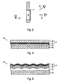
- Fig.1 shows a schematic representation of a banknote 10 with a through opening 14, which is covered with a see-through security element 12 in the form of a strip.
- the Figures 2 and 3 show the bill 10 along the line II-II of Fig.1 in cross section when viewed in reflected light ( Fig. 2 ) or transmitted light ( Fig. 3 ).
- the see-through security element 12 shows when viewed a visually attractive reflected light / transmitted light effect, which visually enhances the security element compared to conventional metallized embossed holograms and also makes much more difficult to adjust. If the see-through security element 12 is viewed in incident light, for example in front of a dark background 20 (FIG. Fig. 2 ), the see-through security element 12 shows a specular, color-neutral metallic hologram 16 both in vertical viewing 22 and in oblique viewing 24. The semitransparency of the see-through security element 12 does not appear in the top view.
- Such a reflected light / transmitted light effect is in contrast to the visual appearance of known optical interference coatings with a color shift effect, like the one in the publication WO 03/070482 A1 described semitransparent interference elements.
- the interference elements of WO 03/070482 A1 always show a color shift effect both on the front and on the back.
- the diffraction effects when viewed in incident light, so when the documents rests for example on a substrate, visually particularly stand out.
- the diffraction effects occur significantly, but the color shift effect is pronounced in reflected light and in transmitted light.
- the see-through security element according to the invention may, but does not necessarily have, to have a hologram. It is important in the context of the present invention, only that the see-through security element in the reflected light substantially neutral in color and without Farbkippable metallic reflective and appears in transmitted light with a semi-transparent color shift effect.
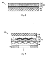
- FIG. 4 shows the layer structure of a see-through security element 40 according to the invention in cross section.
- the see-through security element 40 includes a thin-film element 42 with a color-shift effect, which contains exactly one metal layer 44 and exactly one dielectric layer 46.
- the metal layer 44 is formed semitransparent with a light transmission between 3% and 70% and may be formed in particular from silver, aluminum, gold, chromium, nickel, copper, potassium, tungsten or an alloy of these metals.
- the metal layer 44 is a 30 nm thick silver layer.
- the dielectric layer 46 may be a low refractive index dielectric layer having a refractive index n ⁇ 1.8, such as SiO 2 or MgF 2 , or a high refractive index dielectric layer with a refractive index n ⁇ 1.8, such as TiO 2 or ZnS.
- the dielectric layer 46 is a 525 nm-thick SiO 2 layer.
- the see-through security element 40 of Fig. 4 viewed in incident light, so only the metallic reflective appearance of the metal layer 44, but no color shift effect can be seen.
- the see-through security element When viewed in transmitted light, the see-through security element exhibits a semi-transparent color shift effect, for example from magenta to green.
- the see-through security element 40 has, on the one hand, a simple structure with the two-layer thin-film element 42, and, on the other hand, shows a supervision / see-through effect which contrasts with conventional thin-film elements with a color-shift effect and increases the recognition value and the forgery-proof security of the see-through security element.
- a film substrate 48 for example a PET film, is provided with a primer / adhesion promoter 45.
- the semitransparent metal layer 44 is evaporated in the form of a generally 25 nm to 35 nm thick silver layer and then the dielectric layer 46 in the form of a generally 500 nm to 550 nm thick SiO 2 layer.
- the order of the coating can also be reversed, so that initially a 500 nm to 550 nm thick SiO 2 layer and then a 25 nm to 30 nm thick silver layer is vapor-deposited on the primer layer 45. The visual impression does not change due to the reversal of the layer order.
- Fig. 5 shows an embodiment of the invention in which a two-layer thin-film element 52 next to a semi-transparent metal layer 54 includes a high-refractive dielectric layer 56.
- the film substrate 58 of the see-through security element 50 in this exemplary embodiment contains an embossing lacquer layer 55 with a hologram embossing structure.
- a primer layer After the application of a primer layer, first the dielectric layer 56 in the form of a 325 nm to 350 nm thick ZnS layer was vapor-deposited onto the film substrate, and then the semitransparent metal layer 54 was vapor-deposited in the form of a silver layer of about 30 nm thickness.
- the see-through security element 50 When viewed in incident light, the see-through security element 50 shows an opaque metal hologram without color-shift effect. In transmitted light, a semi-transparent color shift effect is visible, which is visible only in the hologram embossing.
- the see-through security element 50 thus combines a simple two-layer structure of the thin-film element 52 with a novel supervision / see-through effect.
- the see-through security element 60 shown has a thin-film element 62 with a three-layer structure which generates a color-shift effect with very strong colors in transmitted light.
- the see-through security element 60 comprises a film substrate 68 with or without embossed structure, a primer layer 65 and a thin-film element 62 having a three-layer structure with the layer sequence: semitransparent metal layer 74, low-refractive dielectric layer 76, high-index dielectric layer 78.
- the semitransparent metal layer 74 was in the form of an approximately 30 nm thick layer of silver evaporated, the low-refractive dielectric layer 76 in the form of a 500 nm to 550 nm thick SiO 2 layer and the high-index dielectric layer 78 in the form of an approximately 50 nm thick ZnS layer.
- the visual impression of the see-through security element 60 largely corresponds to that of the see-through security element 40 of FIG Fig. 4
- the additionally provided high refractive dielectric layer 78 leads to a color shift effect with particularly strong colors.
- the interface of the dielectric layers 76, 78 each reflects a portion of light back to the metal layer 74, thus causing multiple absorption within a light path.
- a large refractive index difference such as for example between ZnS as a high-index dielectric layer and MgF 2 as a low-index dielectric layer, is advantageous.
- Fig. 7 shows the use of a variant of the see-through security element of Fig. 6 to cover a continuous opening of a banknote 10.
- the illustrated see-through security element 80 has a foil substrate 88 with an embossing lacquer layer 85 with a hologram embossing structure.
- On the film substrate 88 is a thin film element 82 having a three-layer structure as in FIG Fig. 6 , ie with the layer sequence: semitransparent metal layer 94, low-refractive-index dielectric layer 96 and high-refractive-index dielectric layer 98.
- the semitransparent metal layer 94 may be present only in regions.
- the thin-film element 62 is further provided with a protective lacquer layer 84 and applied to the banknote 10 via an adhesive layer 86 in the region of the opening 14.
- the see-through security element 80 When viewed in incident light, the see-through security element 80 shows an opaque metal hologram with no color shift effect, as in Fig. 2 described. In transmitted light, a semitransparent color shift effect with very strong colors, as always with Fig. 3 described.
- the color transmission is as follows: Dielectric layers can block regions of the visible spectrum in the transmission, so that the reflection appears colored. Since no light is absorbed, the transmission includes the complementary color of the reflection. If a dielectric layer is combined with a selectively absorbing optical element which absorbs part of the visible spectral range, then the reflection no longer has to be color-complementary to the transmission. On the contrary, such a combination may appear colorless in reflection, but may have a color in transmission.
- the selectively absorbing optical element is formed by a very thin metal layer having a thickness of less than 100 nm.
- the selective optical absorption in the visible spectral range unlike conventional color-shifting structures, relies not on the interference of multiply reflected light beams, but on an intrinsic property of metals, namely the fact that metals are for light with a higher frequency than the plasma frequency of the metal become transparent.
- the influence on the transmission in the visible spectral range is greater, the closer the plasma frequency is to the visible range.
- Light whose frequency corresponds to the plasma resonance is absorbed more intensely and increase the transmission for the same wavelength range.
- the color effect of the metal layer alone is approximately independent of the angle of incidence of the light or of the viewing angle of the observer.
- the transmitted color hardly changes when the layer thickness of the metal layer is changed. A change in the layer thickness has primarily only on the color intensity.
- Table 1 metal colour color difference Tmax pabs Ag blue 0.11 330nm 240-280 nm al blue 0.07 950 nm 830 nm Au yellow 0.09 540-600 nm - Cr slightly blue 0.03 - 600 nm Ni slightly blue 0.04 370 nm - Cu reddish 0.05 590 nm 250 nm K blue 12:07 in the blue in the blue W reddish 0.01 red blue
- the metals silver, gold, aluminum, potassium and copper are particularly color intensive (large color difference to the white point).
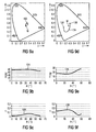
- the emission spectrum of a D65 lamp was used, which roughly corresponds to the color spectrum of daylight.
- FIGS. 8 (a) and (d) in each case the CIE xy color chart, in which the spectral color band 100, on which spectral colors lie, includes all color gradients perceptible to the human eye, given in each case by hue and saturation, for a specific brightness.
- the colors red at 630 nm, yellow at 570 nm, green at 520 nm and blue at 480 nm are marked on the spectral color train 100 by specifying the wavelength.
- the spectral color train 100 is closed by the purple line 102.
- FIGS. 8 (b) and (e) show as a function of the layer thickness d of the silver layer, the proportion of the reflected light R and transmitted light T in percent.
- the reflection or the transmission has already been weighted with the sensitivity of the human eye and therefore corresponds to the L value of the Lab color space.
- Curves 104 and 106 show the proportion of the reflected light and the transmitted light, respectively.
- the color location of the transmitted light is indicated by the curve 114 in FIG Fig. 8 (d) shown.
- the color location of the transmission moves from the white point W into the blue, approximately in the direction of the 480 nm mark on the spectral color band 100, so that the transmitted light appears clearly blue at a layer thickness above 25 nm.
- the effect of color generation through a very thin metal layer as a selectively absorbing optical element is inventively combined with dielectric layers, on the one hand to enhance the color and on the other hand additionally to realize a color shift effect.
- Particularly strong effects are achieved when two different dielectric layers with a dielectric interface are provided, which redirects some of the light back to the metal layer as efficiently as possible to effect multiple absorption in a light path, such as those discussed above the FIGS. 6 and 7 described designs.
- the simulation underlying structure largely corresponds to the see-through security element 60 of Fig. 6 , but with the reverse layer sequence of the thin-film element 62, so that the top view is made on the thin silver layer.
- FIGS. 9 (a) to (f) represent the brightness and color of this layer sequence as a function of the light incidence direction, expressed by the Polar angle ⁇ for reflection in reflection (left half of the figure, Fig. 9 (a), (b), (c) ) or in transmission (right half of the figure, Fig. 9 (d), (e), (f) ).
- FIGS. 9 (a) and (d) each color locus in the CIE xy color chart As in Fig. 8 showed the FIGS. 9 (a) and (d) each color locus in the CIE xy color chart, the FIGS. 9 (b) and (e) the proportion of the reflected light R and transmitted light T and the FIGS. 9 (c) and (f) the color F of the reflected or transmitted light, expressed by the distance of the respective color locus from the white point W in the CIE-xy color chart.
- Curves 124 and 126 indicate the proportion of the reflected light and the transmitted light, respectively.
- the fraction of the reflected light is always between 70% and 80% for angles of incidence between 0 ° (vertical incidence) and 60 ° (curve 124), the proportion of transmitted light is between 15% and slightly more than 25% (curve 126).
- the color of the transmitted light and the color shift effect is from the FIGS. 9 (d) and (f) to recognize.
- the color difference of the transmitted light from the white point W is always greater than 0.10 up to a tilt angle of about 45 °, in some areas even greater than 0.15.
- the specified layer sequence therefore shows in transmission strong colors and a pronounced color shift effect.
- the color and the color change of the reflected light are much lower, as in the FIGS. 9 (a) and (c) shown.
- the in Fig. 9 (a) the color locus indicated by the curve 132 changes from a desaturated orange color locus in a perpendicular direction of incidence with an increasing tilt angle over weak green tones to a pale blue near the white point W in an oblique viewing direction.
- the color difference of the reflected light from the white point W is always less than 0.08, for the most part even less than 0.05.
- the specified layer sequence therefore shows in reflection only very weak, almost completely desaturated colors, which visually hardly stand out against the background of the metallic reflection. Due to the small deviation of the color locations from the white point, the color change of the desaturated colors during tilting practically does not occur.
- Fig. 10 shows a polymer banknote 140 with a printing area 142 and a transparent area 144 in which a see-through security element 150 according to the invention with the incident light / transmitted-light effect described above is applied.
- the see-through security element 150 has a releasable film substrate 158, which is provided with an embossing lacquer layer 155 with a hologram embossing structure and a thin-film element 152.
- the thin-film element 152 has a three-layer structure with the layer sequence: semitransparent Metal layer 164, such as aluminum or silver, low refractive dielectric layer 166, such as MgF 2 or SiO 2 , and high refractive dielectric layer 168, such as ZnS.
- the semitransparent metal layer 164 may also include recesses 162 in the form of patterns, characters, or a coding, such as those shown in FIG Fig. 10 shown letter sequence "PL", have.
- the thin-film element 152 is provided with a protective lacquer layer 154 and applied to the polymer banknote 140 via an adhesive layer 156 in the transparent region 144. After the transfer, the film substrate 158 is peeled off, as indicated by the reference numeral 160.
- FIGS. 12 and 13 show two variants in which inventive see-through security elements are combined with hybrid substrates, such as composite film banknotes.
- Figure 12 1 shows a composite film banknote 170 having a first PET film 172, a paper layer 174 and a second PET film 176.
- a see-through security element 180 of the type described above is embedded in the paper layer 174 in a window region 178 of the film composite banknote 170.
- the see-through security element 180 is applied in the region of the window 178 to the second PET film 176 of the film composite banknote 170.
- the see-through security element 180 includes a releasable film substrate 182 which is peeled off after transfer, as indicated by reference numeral 184.
- Transparent safety elements according to the invention can also be used with cards, provided that they are at least partially transparent.
- Fig. 14 shows a card 190, in which a see-through security element 180 of described above in a transparent area on the surface of the card 190 is applied.
- the releasable film substrate 182 of the see-through security element 180 is peeled off after the transfer (reference numeral 184).
- a see-through security element 192 according to the invention may also be embedded in an inner layer 194 of the card 190, as in FIG Fig. 15 shown.
- the see-through security element according to the invention has mostly been combined, for example, with a hologram structure. It will be understood, however, that this variant is illustrative only and that combinations with other diffractive microstructures such as holographic grating images or hologram-like diffraction structures may be used, or with micro-optic relief structures such as blazed grids, Fresnel structures, lens or micromirror structures , In addition to microrelief structures on the order of the wavelength of light, microstructures with smaller structural elements are also suitable for such a combination, such as sub-wavelength gratings or moth-eye structures, whose structural elements may also be smaller than 100 nm.
Abstract
Description
Die Erfindung betrifft ein Durchsichtssicherheitselement für Sicherheitspapiere, Wertdokumente und dergleichen, ein Verfahren zur Herstellung eines derartigen Durchsichtssicherheitselements sowie einen mit einem solchen Durchsichtssicherheitselement ausgestatteten Datenträger.The invention relates to a see-through security element for security papers, documents of value and the like, a method for producing such a see-through security element and equipped with such a see-through security element data carriers.
Datenträger, wie etwa Wert- oder Ausweisdokumente, oder andere Wertgegenstände, wie etwa Markenartikel, werden zur Absicherung oft mit Sicherheitselementen versehen, die eine Überprüfung der Echtheit der Datenträger gestatten und die zugleich als Schutz vor unerlaubter Reproduktion dienen. Die Sicherheitselemente können beispielsweise in Form eines in eine Banknote eingebetteten Sicherheitsfadens, eines Aufreißfadens für Produktverpackungen, eines aufgebrachten Sicherheitsstreifens, einer Abdeckfolie für eine Banknote mit einer durchgehenden Öffnung oder eines selbsttragenden Transferelements ausgebildet sein, wie etwa einem Patch oder einem Etikett, das nach seiner Herstellung auf ein Wertdokument aufgebracht wird.Data carriers, such as valuables or identity documents, or other valuables, such as branded articles, are often provided with security elements for the purpose of security, which permit verification of the authenticity of the data carriers and at the same time serve as protection against unauthorized reproduction. The security elements may be in the form of, for example, a security thread embedded in a banknote, a tearing thread for product packaging, an applied security strip, a cover sheet for a banknote having a through opening or a self-supporting transfer element, such as a patch or label after its manufacture is applied to a document of value.
Seit einigen Jahren haben sich Durchsichtsfenster als attraktive Sicherheitselemente in Polymer- und neuerdings auch in Papier-Banknoten erwiesen, da sie den Einsatz einer Vielzahl von Sicherheitsmerkmalen gestatten. Eine besondere Rolle bei der Echtheitsabsicherung spielen Sicherheitselemente mit betrachtungswinkelabhängigen Effekten, da diese selbst mit modernsten Kopiergeräten nicht reproduziert werden können. Die Sicherheitselemente werden dabei mit optisch variablen Elementen ausgestattet, die dem Betrachter unter unterschiedlichen Betrachtungswinkeln einen unterschiedlichen Bildeindruck vermitteln und beispielsweise je nach Betrachtungswinkel einen anderen Farb- oder Helligkeitseindruck und/ oder ein anderes graphisches Motiv zeigen.For some years, see-through windows have proven to be attractive security features in polymer and, more recently, in paper banknotes as they allow the use of a variety of security features. Security elements with viewing-angle-dependent effects play a special role in the authentication of authenticity since they can not be reproduced even with the most modern copiers. The security elements are thereby equipped with optically variable elements that give the viewer a different image impression under different viewing angles and, for example, show a different color or brightness impression and / or another graphic motif depending on the viewing angle.
Die Aufgabe der vorliegenden Erfindung liegt nun darin, ein gattungsgemäßes Durchsichtssicherheitselement anzugeben, das die Nachteile des Standes der Technik vermeidet. Insbesondere soll das Durchsichtssicherheitselement ein ansprechendes visuelles Erscheinungsbild mit hoher Fälschungssicherheit verbinden.The object of the present invention is therefore to provide a generic see-through safety element which avoids the disadvantages of the prior art. In particular, the see-through security element should combine an appealing visual appearance with high security against counterfeiting.
Diese Aufgabe wird durch das Durchsichtssicherheitselement, das Herstellungsverfahren und den Datenträger mit den Merkmalen der unabhängigen Ansprüche gelöst. Weiterbildungen der Erfindung sind Gegenstand der Unteransprüche.This object is achieved by the see-through security element, the manufacturing method and the data carrier having the features of the independent claims. Further developments of the invention are the subject of the dependent claims.
Gemäß der Erfindung weist ein Durchsichtssicherheitselement der eingangs genannten Art ein Dünnschichtelement mit Farbkippeffekt auf, das genau eine Metallschicht und zumindest eine Dielektrikumsschicht enthält, wobei die Metallschicht semitransparent ausgebildet ist. Unter "Semitransparenz" ist dabei Transluzenz zu verstehen, insbesondere eine Lichtdurchlässigkeit zwischen 3 % und 80 %.According to the invention, a see-through security element of the type mentioned in the beginning has a thin-film element with a color-shift effect which contains precisely one metal layer and at least one dielectric layer, the metal layer being semitransparent. By "semitransparency" is meant translucency, in particular a light transmission between 3% and 80%.
Wie nachfolgend genauer erläutert, weist das Durchsichtssicherheitselement im Auflicht einen metallisch spiegelnden und im Durchlicht einen farbigen visuellen Eindruck auf. Insbesondere erscheint das Durchsichtssicherheitselement im Auflicht metallisch spiegelnd und farbneutral und erscheint im Durchlicht farbig. Besonders bevorzugt ist die farbige Transmission mit einem Farbkippeffekt kombiniert, so dass das Durchsichtssicherheitselement im Durchlicht je nach Betrachtungswinkel mit einer unterschiedlichen Farbe erscheint und so einen semitransparenten Farbkippeffekt aufweist.As explained in more detail below, the see-through security element in reflected light on a metallic reflective and in transmitted light a colored visual impression. In particular, the see-through security element appears metallically specular and color-neutral in reflected light and appears colored in the transmitted light. Particularly preferably, the colored transmission is combined with a color shift effect, so that the see-through security element appears in transmitted light depending on the viewing angle with a different color and thus has a semi-transparent color shift effect.
Die Farbigkeit transmittierten bzw. reflektierten Lichts kann durch Angabe eines Farborts in einem Farbsystem quantifiziert werden. Im Rahmen dieser Anmeldung wird die Farbigkeit F durch den Abstand der Normfarbwertanteile x, y der Farbe zum Weißpunkt (x = y =1/3) im CIE-Normvalenzsystem angegeben.The color of transmitted or reflected light can be quantified by specifying a color locus in a color system. In the context of this The colouration F is indicated by the distance of the standard chromaticity coordinates x, y of the color to the white point (x = y = 1/3) in the CIE standard valence system.
Dabei weist das erfindungsgemäße Durchsichtssicherheitselement im Auflicht bei senkrechter Betrachtung bevorzugt eine Farbigkeit F < 0,10, besonders bevorzugt F < 0,05 auf. Das Durchsichtssicherheitselement zeigt dann im Auflicht nur schwache, fast vollständig entsättigte Farben, die vor dem Hintergrund der metallischen Reflexion der semitransparenten Metallschicht visuell kaum auffallen.In the incident light, the see-through security element according to the invention preferably has a colouration F <0.10, particularly preferably F <0.05, when viewed perpendicularly. The see-through security element then shows in reflected light only weak, almost completely desaturated colors, which hardly visually stand against the background of the metallic reflection of the semitransparent metal layer.
Mit Vorteil bleibt der Farbeindruck beim Kippen des Durchsichtssicherheitselements stets schwach, wobei das Durchsichtssicherheitselement vorzugsweise im Auflicht im Winkelbereich zwischen 0° und 60° stets eine Farbigkeit F < 0,10 aufweist.Advantageously, the color impression always remains weak when tilting the see-through security element, the see-through security element preferably always having a color F <0.10 in reflected light in the angular range between 0 ° and 60 °.
Anders als die Reflexion ist die Transmission des Durchsichtssicherheitselements farbig, wobei das Durchsichtssicherheitselement im Durchlicht bei senkrechter Betrachtung bevorzugt eine Farbigkeit F > 0,05, besonders bevorzugt F > 0,10 aufweist. Mit Vorteil bleibt der starke Farbeindruck für einen weiten Bereich der im Durchlicht sichtbaren Farbe bzw. des im Durchlicht sichtbaren Farbkippeffekts erhalten. Insbesondere weist das Durchsichtssicherheitselement im Durchlicht im Winkelbereich zwischen 0° und 40° stets eine Farbigkeit F > 0,05, vorzugsweise F > 0,10 auf.Unlike the reflection, the transmission of the see-through security element is colored, wherein the see-through security element in transmitted light when viewed perpendicularly preferably has a color F> 0.05, particularly preferably F> 0.10. Advantageously, the strong color impression is retained for a wide range of the visible color in transmitted light or the visible in the transmitted light color shift effect. In particular, the see-through security element in transmitted light in the angular range between 0 ° and 40 ° always a colouration F> 0.05, preferably F> 0.10.
Die Schichtdicke der semitransparenten Metallschicht liegt vorzugsweise zwischen 5 nm und 70 nm, wobei für Silberschichten der Dickenbereich zwischen 15 nm und 50 nm, für Aluminiumschichten der Dickenbereich zwischen 5 nm und 15 nm und für Goldschichten der Dickenbereich zwischen 30 nm und 70 nm besonders bevorzugt ist. Neben den Metallen Silber, Aluminium und Gold kann die semitransparente Metallschicht insbesondere auch aus Chrom, Nickel, Kupfer, Kalium, Wolfram oder einer Legierung dieser Metalle gebildet sein. Eine besonders farbintensive Transmission lässt sich mit semitransparenten Metallschichten aus Silber, Aluminium, Gold, Kalium oder Kupfer erreichen.The layer thickness of the semitransparent metal layer is preferably between 5 nm and 70 nm, wherein the thickness range between 15 nm and 50 nm for silver layers, the thickness range between 5 nm and 15 nm for aluminum layers and the thickness range between 30 nm and 70 nm is particularly preferred. In addition to the metals silver, aluminum and gold, the semitransparent metal layer may in particular also be formed from chromium, nickel, copper, potassium, tungsten or an alloy of these metals. A particularly color-intensive transmission can be achieved with semitransparent metal layers of silver, aluminum, gold, potassium or copper.
Allgemein kommen für die semitransparente Metallschicht vor allem solche Metalle infrage, deren Plasmafrequenz im ultravioletten, sichtbaren oder nahinfraroten Spektralbereich liegt. Die Plasmafrequenz ωp ist dabei die Frequenz der longitudinalen Schwingungen des Elektrongases gegenüber den Ionenrümpfen. Beispielsweise entspricht die Plasmafrequenz von Silber einer Wellenlänge von 311 nm (Ultraviolett), die Plasmafrequenz von Gold einer Wellenlänge von 560 nm (Sichtbar) und die Plasmafrequenz von Aluminium einer Wellenlänge von 830 nm (nahes Infrarot).In general, for the semitransparent metal layer, in particular those metals are considered whose plasma frequency lies in the ultraviolet, visible or near-infrared spectral range. The plasma frequency ω p is the frequency of the longitudinal oscillations of the electron gas relative to the ion bodies. For example, the plasma frequency of silver corresponds to a wavelength of 311 nm (ultraviolet), the plasma frequency of gold to a wavelength of 560 nm (visible), and the plasma frequency of aluminum to a wavelength of 830 nm (near infrared).
In einer vorteilhaften Ausgestaltung der Erfindung ist die semitransparente Metallschicht homogen, also insbesondere nicht in Form von metallischen Inseln bzw. Clustern ausgebildet, und ermöglicht so ein einfaches Aufbringen, beispielsweise durch Aufdampfen in einem Vakuumbeschichtungsverfahren.In an advantageous embodiment of the invention, the semitransparent metal layer is homogeneous, ie in particular not formed in the form of metallic islands or clusters, and thus allows easy application, for example by vapor deposition in a vacuum coating process.
Die semitransparente Metallschicht bildet insbesondere ein im sichtbaren Spektralbereich selektiv absorbierendes optisches Element. Wie in der gegenwärtigen Erfindung erkannt, kann durch eine Kombination einer oder mehrerer dielektrischer Schichten mit einem selektiv absorbierenden optischen Element ein semitransparentes Durchsichtssicherheitselement geschaffen werden, dessen Transmissions- und Reflexionsfarben nicht komplementär zueinander sein müssen. Die dielektrischen Schichten und das selektiv absorbierende optische Element können vielmehr mit Vorteil so aufeinander abgestimmt werden, dass das Durchsichtssicherheitselement in Reflexion im Wesentlichen farbneutral erscheint und in Transmission einen kräftigen Farbeindruck erzeugt. Dabei hängt der Farbton des transmittierten Lichts nicht empfindlich von der Schichtdicke der semitransparenten Metallschicht ab, so dass dieser Parameter bei der Herstellung nicht kritisch ist.The semitransparent metal layer forms in particular a selectively absorbing optical element in the visible spectral range. As recognized in the present invention, by combining one or more dielectric layers with a selectively absorbing optical element, a semitransparent see-through security element can be provided whose transmission and reflection colors need not be complementary to one another. The dielectric layers and the selective On the contrary, absorbing optical elements can advantageously be matched to one another in such a way that the see-through security element appears substantially neutral in color in reflection and produces a strong color impression in transmission. In this case, the hue of the transmitted light is not sensitive to the layer thickness of the semitransparent metal layer, so that this parameter is not critical in the production.
In einer vorteilhaften Erfindungsvariante ist das Dünnschichtelement des Durchsichtssicherheitselements ein zweischichtiges Dünnschichtelement, das neben der semitransparenten Metallschicht genau eine Dielektrikumsschicht enthält.In an advantageous variant of the invention, the thin-film element of the see-through security element is a two-layered thin-film element which contains precisely one dielectric layer in addition to the semitransparent metal layer.
Bei einer anderen ebenfalls vorteilhaften Erfindungsvariante ist das Dünnschichtelement ein dreischichtiges Dünnschichtelement, das neben der semitransparenten Metallschicht zwei auf gegenüberliegenden Seiten der Metallschicht angeordnete Dielektrikumsschichten enthält. Die beiden Dielektrikumsschichten sind dabei mit Vorteil hochbrechend mit einem Brechungsindex n ≥ 1,8.In another likewise advantageous variant of the invention, the thin-film element is a three-layered thin-film element which, in addition to the semitransparent metal layer, contains two dielectric layers arranged on opposite sides of the metal layer. The two dielectric layers are advantageously high-refractive with a refractive index n ≥ 1.8.
Nach einer weiteren ebenfalls vorteilhaften Erfindungsvariante ist das Dünnschichtelement ein dreischichtiges Dünnschichtelement, das neben der semitransparenten Metallschicht zwei übereinander auf derselben Seite der Metallschicht angeordnete Dielektrikumsschichten enthält. Dabei ist mit Vorteil die direkt auf der semitransparenten Metallschicht angeordnete erste Dielektrikumsschicht niedrigbrechend mit einem Brechungsindex n < 1,8 und die auf der ersten Dielektrikumsschicht angeordnete zweite Dielektrikumsschicht hochbrechend mit einem Brechungsindex n ≥ 1,8.According to a further likewise advantageous variant of the invention, the thin-film element is a three-layered thin-film element which, in addition to the semitransparent metal layer, contains two dielectric layers arranged one above the other on the same side of the metal layer. In this case, advantageously, the first dielectric layer arranged directly on the semitransparent metal layer is low-refractive with a refractive index n <1.8 and the second dielectric layer arranged on the first dielectric layer is high-refractive with a refractive index n ≥ 1.8.
Allgemein sind bei der oder den direkt auf der semitransparenten Metallschicht angeordnete(n) Dielektrikumsschicht(en) die Schichtdicke d und der Brechungsindex n vorzugsweise so aufeinander abgestimmt, dass das Produkt d*n zwischen 300 nm und 800 nm liegt. Die auf der ersten Dielektrikumsschicht angeordnete zweite Dielektrikumsschicht weist mit Vorteil eine Schichtdicke zwischen 30 nm und 100 nm auf.In general, in the case of the dielectric layer (s) arranged directly on the semitransparent metal layer, the layer thickness d and the refractive index n are preferably matched to one another such that the product d * n is between 300 nm and 800 nm. The second dielectric layer arranged on the first dielectric layer advantageously has a layer thickness between 30 nm and 100 nm.
Beispiele für hochbrechende Dielektrikumsschichten sind ZnS-Schichten oder TiO2-Schichten niedrigbrechende Dielektrikumsschichten können beispielsweise aus SiO2 oder MgF2 gebildet sein.Examples of high-index dielectric layers are ZnS layers or TiO 2 layers. Low-refractive dielectric layers can be formed, for example, from SiO 2 or MgF 2 .
In allen Ausgestaltungen kann die semitransparente Metallschicht Aussparungen in Form von Mustern, Zeichen oder Codierungen aufweisen, um beispielsweise eine zusätzliche Information in dem Durchsichtssicherheitselement darzustellen. Weiter kann das Dünnschichtelement in allen Ausgestaltungen mit einer diffraktiven Beugungsstruktur kombiniert sein, wobei die semitransparente Metallschicht die Metallisierungsschicht der Beugungsstruktur bildet. Die diffraktive Beugungsstruktur kann insbesondere ein Hologramm, ein holographisches Gitterbild, eine geblazede Beugungsstruktur, ein computergeneriertes Hologramm (CGH) oder eine andere hologrammähnliche Beugungsstruktur darstellen. Daneben kommen auch andere Kombinationen, etwa mit Jalousiestrukturen oder mit achromatischen Strukturen, wie etwa einer Mattstruktur, einer Mikrospiegelanordnung, einem Blazegitter mit einem sägezahnartigen Furchenprofil oder einer Fresnellinsen-Anordnung und/ oder einer mikrooptischen Reliefstruktur infrage.In all embodiments, the semitransparent metal layer may have recesses in the form of patterns, characters or codes, for example to represent additional information in the see-through security element. Furthermore, in all embodiments, the thin-film element may be combined with a diffractive diffraction structure, wherein the semitransparent metal layer forms the metallization layer of the diffraction structure. The diffractive diffraction structure may in particular represent a hologram, a holographic grating image, a blazed diffraction structure, a computer-generated hologram (CGH) or another hologram-like diffraction structure. In addition, other combinations, such as with blind structures or with achromatic structures, such as a matte structure, a micromirror arrangement, a Blazegitter with a sawtooth-like furrow profile or Fresnellinsen arrangement and / or a micro-optical relief structure in question.
Die Erfindung enthält auch ein Verfahren zum Herstellen eines Durchsichtssicherheitselements der beschriebenen Art, bei dem ein Dünnschichtelement mit Farbkippeffekt erzeugt wird, indem genau eine semitransparent ausgebildete Metallschicht mit zumindest einer Dielektrikumsschicht kombiniert wird. Die semitransparente Metallschicht und die zumindest eine Dielektrikumsschicht werden dabei zweckmäßig auf einen Träger, beispielsweise ein Foliensubstrat, aufgebracht, insbesondere durch ein Vakuumbeschichtungsverfahren aufgedampft. Das Foliensubstrat kann dabei mit einer gewünschten Relief- oder Prägestruktur versehen und beispielsweise mit einem Primer/Haftvermittler beschichtet sein. Nach dem Übertragen des Durchsichtssicherheitselements auf ein Zielsubstrat kann der Träger von dem Sicherheitselement abgelöst werden.The invention also includes a method for producing a see-through security element of the type described, in which a thin-film element with a color-shift effect is produced by exactly one semitransparent design Metal layer is combined with at least one dielectric layer. The semitransparent metal layer and the at least one dielectric layer are expediently applied to a carrier, for example a film substrate, in particular vapor-deposited by a vacuum coating method. The film substrate can be provided with a desired relief or embossed structure and coated, for example, with a primer / adhesion promoter. After transferring the see-through security element to a target substrate, the carrier can be detached from the security element.
Die Erfindung enthält ferner einen Datenträger mit einem Durchsichtssicherheitselement der oben beschriebenen Art, wobei das Durchsichtssicherheitselement insbesondere in oder über einem transparenten Fensterbereich oder einer durchgehenden Öffnung des Datenträgers angeordnet ist. Bei dem Datenträger kann es sich insbesondere um ein Wertdokument, wie eine Banknote, insbesondere eine Papierbanknote, eine Polymerbanknote oder eine Folienverbundbanknote, handeln, oder um eine Ausweiskarte, wie etwa eine Kreditkarte, Bankkarte, Barzahlungskarte, Berechtigungskarte, einen Personalausweis oder eine Passpersonalisierungsseite handeln.The invention further includes a data carrier with a see-through security element of the type described above, wherein the see-through security element is arranged in particular in or over a transparent window area or a through opening of the data carrier. The data carrier may in particular be a value document, such as a banknote, in particular a paper banknote, a polymer banknote or a film composite banknote, or an identification card, such as a credit card, bank card, cash card, authorization card, identity card or passport personalization page.
Weitere Ausführungsbeispiele sowie Vorteile der Erfindung werden nachfolgend anhand der Figuren erläutert, bei deren Darstellung auf eine maßstabs- und proportionsgetreue Wiedergabe verzichtet wurde, um die Anschaulichkeit zu erhöhen. Die verschiedenen Ausführungsbeispiele sind nicht auf die Verwendung in der konkret beschriebenen Form beschränkt, sondern können auch untereinander kombiniert werden.Further embodiments and advantages of the invention will be explained below with reference to the figures, the representation has been dispensed to scale and proportionate reproduction in order to increase the clarity. The various embodiments are not limited to use in the specific form described, but can also be combined with each other.
Es zeigen:
- Fig.1
- eine schematische Darstellung einer Banknote mit einem erfindungsgemäßen Durchsichtssicherheitselement,
- Fig. 2
- schematisch einen Schnitt entlang der Linie II-II von
Fig.1 bei Betrachtung im Auflicht, - Fig. 3
- schematisch einen Schnitt entlang der Linie II-II von
Fig.1 bei Betrachtung im Durchlicht, - Fig. 4
- ein Durchsichtssicherheitselement nach einem Ausführungsbeispiel der Erfindung,
- Fig. 5
- ein Ausführungsbeispiel der Erfindung mit einem zweischichtigen Dünnschichtelement,
- Fig. 6
- ein erfindungsgemäßes Durchsichtssicherheitselement mit einem Dünnschichtelement mit Dreischichtaufbau,
- Fig. 7
- die Verwendung einer Variante des Durchsichtssicherheitselements der
Fig. 6 zur Abdeckung einer durchgehenden Öffnung einer Banknote, - Fig. 8
- die Ergebnisse einer numerischen Simulation für dünne Silberschichten (d = 5
nm bis 40 nm) in einer dielektrischen Umgebung mit Brechungsindex n = 1,5 bei senkrechter Betrachtung in Reflexion ((a), (b), (c)) bzw. in Transmission ((d), (e), (f)), wobei
(a) und (d) jeweils die CIE-xy-Farbtafel,
(b) und (e) den Anteil des reflektierten Lichts R bzw. transmittierten Lichts T in Abhängigkeit von der Schichtdicke d der Silberschicht, und
(c) und (f) die Farbigkeit F des reflektierten bzw. transmittierten Lichts in Abhängigkeit von der Schichtdicke d der Silberschicht zeigen, - Fig. 9
- die Ergebnisse einer numerischen Simulation für eine dünne Silberschicht (d = 25 nm), die über einer niedrigbrechenden Dielektrikumsschicht in Form einer 500 nm dicken MgF2-Schicht, einer hochbrechenden Dielektrikumsschicht in Form einer 50 nm dicken ZnS-Schicht und einem Dielektrikum mit n = 1,5 angeordnet ist, bei Betrachtung in Reflexion ((a), (b), (c)) bzw. in Transmission ((d), (e), (f)), wobei
(a) und (d) jeweils die CIE-xy-Farbtafel,
(b) und (e) den Anteil des reflektierten Lichts R bzw. transmittierten Lichts T in Abhängigkeitvon der Lichteinfallsrichtung 0, und
(c) und (f) die Farbigkeit F des reflektierten bzw. transmittierten Lichts in Abhängigkeit von der Lichteinfallsrichtung θ zeigen, - Fig. 10
- eine Polymerbanknote mit einem erfindungsgemäßen Durchsichtssicherheitselement,
- Fig. 11
- schematisch einen Schnitt entlang der Linie XI-XI von
Fig. 10 , - Fig. 12,13
- zwei Varianten, bei denen erfindungsgemäße Durchsichtssicherheitselemente mit Hybridsubstraten kombiniert sind, und
- Fig. 14,15
- zwei Varianten, bei denen erfindungsgemäße Durchsichtssicherheitselemente bei Karten eingesetzt sind.
- Fig.1
- a schematic representation of a banknote with a see-through security element according to the invention,
- Fig. 2
- schematically a section along the line II-II of
Fig.1 when viewed in reflected light, - Fig. 3
- schematically a section along the line II-II of
Fig.1 when viewed in transmitted light, - Fig. 4
- a see-through security element according to an embodiment of the invention,
- Fig. 5
- An embodiment of the invention with a two-layer thin-film element,
- Fig. 6
- an inventive see-through safety element with a thin-film element with three-layer structure,
- Fig. 7
- the use of a variant of the see-through security element of
Fig. 6 for covering a through opening of a banknote, - Fig. 8
- the results of a numerical simulation for thin silver layers (d = 5 nm to 40 nm) in a dielectric environment with refractive index n = 1.5 when viewed vertically in reflection ((a), (b), (c)) or in transmission ((d), (e), (f)), where
(a) and (d) each the CIE xy color chart,
(b) and (e) the proportion of the reflected light R or transmitted light T as a function of the layer thickness d of the silver layer, and
(c) and (f) show the color F of the reflected or transmitted light as a function of the layer thickness d of the silver layer, - Fig. 9
- the results of a numerical simulation for a thin silver layer (d = 25 nm), over a low-refractive dielectric layer in the form of a 500 nm thick MgF 2 layer, a high refractive index dielectric layer in the form of a 50 nm thick ZnS layer and a dielectric with n = 1.5, when viewed in reflection ((a), (b), (c)) and in transmission ((d), (e), (f)), respectively
(a) and (d) each the CIE xy color chart,
(b) and (e) the proportion of the reflected light R and transmitted light T as a function of thelight incident direction 0, and
(c) and (f) show the chromaticity F of the reflected or transmitted light as a function of the light incident direction θ, - Fig. 10
- a polymer banknote with a see-through security element according to the invention,
- Fig. 11
- schematically a section along the line XI-XI of
Fig. 10 . - Fig. 12,13
- two variants in which see-through security elements according to the invention are combined with hybrid substrates, and
- Fig. 14, 15
- two variants in which inventive see-through security elements are used in maps.
Die Erfindung wird nun am Beispiel von Sicherheitselementen für Banknoten erläutert.
Das Durchsichtssicherheitselement 12 zeigt bei der Betrachtung einen visuell attraktiven Auflicht/Durchlicht-Effekt, der das Sicherheitselement gegenüber herkömmlichen metallisierten Prägehologrammen optisch aufwertet und auch erheblich schwieriger nachstellbar macht. Wird das Durchsichtssicherheitselement 12 im Auflicht betrachtet, etwa vor einem dunklen Untergrund 20 (
Wird die Banknote dagegen im Durchlicht 30 betrachtet, wie in
Ein solcher Auflicht/Durchlicht-Effekt steht im Gegensatz zu dem visuellen Erscheinungsbild bekannter optischer Interferenzbeschichtungen mit Farbkippeffekt, wie etwa den in der Druckschrift
Das erfindungsgemäße Durchsichtssicherheitselement kann, muss jedoch nicht unbedingt ein Hologramm aufweisen. Wichtig ist im Rahmen der vorliegenden Erfindung lediglich, dass das Durchsichtssicherheitselement im Auflicht im Wesentlichen farbneutral und ohne Farbkippeffekt metallisch spiegelnd und im Durchlicht mit einem semitransparenten Farbkippeffekt erscheint.The see-through security element according to the invention may, but does not necessarily have, to have a hologram. It is important in the context of the present invention, only that the see-through security element in the reflected light substantially neutral in color and without Farbkippeffekt metallic reflective and appears in transmitted light with a semi-transparent color shift effect.
Als Ausführungsbeispiel ohne Hologramm zeigt
Die Metallschicht 44 ist semitransparent mit einer Lichtdurchlässigkeit zwischen 3 % und 70 % ausgebildet und kann insbesondere aus Silber, Aluminium, Gold, Chrom, Nickel, Kupfer, Kalium, Wolfram oder einer Legierung dieser Metalle gebildet sein. Im Ausführungsbeispiel der
Wird das Durchsichtssicherheitselement 40 der
Zur Herstellung eines Durchsichtssicherheitselements der in
Das Foliensubstrat 58 des Durchsichtssicherheitselements 50 enthält in diesem Ausführungsbeispiel eine Prägelackschicht 55 mit einer Hologrammprägestruktur. Nach dem Aufbringen einer Primerschicht wurde auf das Foliensubstrat zunächst die Dielektrikumsschicht 56 in Form einer 325 nm bis 350 nm dicken ZnS-Schicht aufgedampft und anschließend die semitransparente Metallschicht 54 in Form einer etwa 30 nm dicken Silberschicht aufgedampft.The
Bei Betrachtung im Auflicht zeigt das Durchsichtssicherheitselement 50 ein opakes Metallhologramm ohne Farbkippeffekt. Im Durchlicht zeigt sich ein semitransparenter Farbkippeffekt, der nur in der Hologrammprägung sichtbar wird. Das Durchsichtssicherheitselement 50 verbindet somit einen einfachen Zweischichtaufbau des Dünnschichtelements 52 mit einem neuartigen Aufsicht/ Durchsicht-Effekt.When viewed in incident light, the see-through
Das in
Das Durchsichtssicherheitselement 60 enthält ein Foliensubstrat 68 mit oder ohne Prägestruktur, eine Primerschicht 65 und ein Dünnschichtelement 62 mit einem Dreischichtaufbau mit der Schichtfolge: semitransparente Metallschicht 74, niedrigbrechende Dielektrikumsschicht 76, hochbrechende Dielektrikumsschicht 78. Die semitransparente Metallschicht 74 wurde im Ausführungsbeispiel in Form einer etwa 30 nm dicken Silberschicht aufgedampft, die niedrigbrechende Dielektrikumsschicht 76 in Form einer 500 nm bis 550 nm dicken SiO2-Schicht und die hochbrechende Dielektrikumsschicht 78 in Form einer etwa 50 nm dicken ZnS-Schicht. Der visuelle Eindruck des Durchsichtssicherheitselements 60 entspricht weitgehend dem des Durchsichtssicherheitselements 40 der
Dies ist nach gegenwärtigem Verständnis darauf zurückzuführen, dass die die Grenzfläche der dielektrischen Schichten 76, 78 jeweils einen Lichtanteil zurück zur Metallschicht 74 reflektiert und so eine mehrfache Absorption innerhalb eines Lichtpfads bewirkt. Für kräftige Farben ist dabei ein großer Brechungsindexunterschied, wie beispielsweise zwischen ZnS als hochbrechender Dielektrikumsschicht und MgF2 als niedrigbrechender Dielektrikumsschicht, vorteilhaft.This is currently believed to be due to the fact that the interface of the
Bei Betrachtung im Auflicht zeigt das Durchsichtssicherheitselement 80 ein opakes Metallhologramm ohne Farbkippeffekt, wie bei
Im Durchlicht zeigt sich ein semitransparenter Farbkippeffekt mit sehr kräftigen Farben, wie grundsätzlich bei
In transmitted light, a semitransparent color shift effect with very strong colors, as always with
Ohne dadurch an eine bestimmte Erklärung gebunden sein zu wollen, kommt die farbige Transmission bei im Wesentlichen farbneutraler Reflexion nach gegenwärtigem Verständnis wie folgt zustande: Dielektrische Schichten können Bereiche des sichtbaren Spektrums in der Transmission blockieren, so dass die Reflexion farbig erscheint. Da kein Licht absorbiert wird, beinhaltet die Transmission die Komplementärfarbe der Reflexion. Wird nun eine dielektrische Schicht mit einem selektiv absorbierenden optischen Element kombiniert, das einen Teil des sichtbaren Spektralbereichs absorbiert, so muss die Reflexion nicht mehr farblich komplementär zur Transmission sein. Eine solche Kombination kann vielmehr in Reflexion farbneutral erscheinen, in Transmission dagegen eine Farbe besitzen.Without wishing to be bound by any particular explanation, the color transmission, with essentially color-neutral reflection, as currently understood, is as follows: Dielectric layers can block regions of the visible spectrum in the transmission, so that the reflection appears colored. Since no light is absorbed, the transmission includes the complementary color of the reflection. If a dielectric layer is combined with a selectively absorbing optical element which absorbs part of the visible spectral range, then the reflection no longer has to be color-complementary to the transmission. On the contrary, such a combination may appear colorless in reflection, but may have a color in transmission.
Das selektiv absorbierende optische Element wird erfindungsgemäß durch eine sehr dünne Metallschicht einer Dicke unterhalb von 100 nm gebildet. Die selektive optische Absorption im sichtbaren Spektralbereich beruht dabei nach gegenwärtigem Verständnis anders als bei herkömmlichen farbkippenden Strukturen nicht auf der Interferenz von mehrfach reflektierten Lichtstrahlen, sondern auf einer intrinsischen Eigenschaft von Metallen, nämlich der Tatsache, dass Metalle für Licht mit einer höheren Frequenz als der Plasmafrequenz des Metalls transparent werden.According to the invention, the selectively absorbing optical element is formed by a very thin metal layer having a thickness of less than 100 nm. The selective optical absorption in the visible spectral range, according to current understanding, unlike conventional color-shifting structures, relies not on the interference of multiply reflected light beams, but on an intrinsic property of metals, namely the fact that metals are for light with a higher frequency than the plasma frequency of the metal become transparent.
Der Einfluss auf die Transmission im sichtbaren Spektralbereich ist dabei umso größer, je näher die Plasmafrequenz am sichtbaren Bereich liegt. Licht, dessen Frequenz der Plasmaresonanz entspricht, wird verstärkt absorbiert und die Transmission für denselben Wellenlängenbereich erhöht. Der Farbeffekt der Metallschicht alleine ist dabei annähernd unabhängig vom Einfallswinkel des Lichtes bzw. vom Betrachtungswinkel des Beobachters. Auch verändert sich die transmittierte Farbe kaum, wenn die Schichtdicke der Metallschicht geändert wird. Eine Änderung der Schichtdicke hat in erster Linie nur Einfluss auf die Farbintensität.The influence on the transmission in the visible spectral range is greater, the closer the plasma frequency is to the visible range. Light whose frequency corresponds to the plasma resonance is absorbed more intensely and increase the transmission for the same wavelength range. The color effect of the metal layer alone is approximately independent of the angle of incidence of the light or of the viewing angle of the observer. Also, the transmitted color hardly changes when the layer thickness of the metal layer is changed. A change in the layer thickness has primarily only on the color intensity.
Die folgende Tabelle zeigt die Ergebnisse numerischer Simulationen der Transmission dünner Metallschichten (d = 5 nm bis 60 nm). Angegeben ist dabei der jeweils der Farbeindruck der Metallschicht, der Abstand der Farbe vom Weißpunkt W in der CIE-xy-Farbtafel bei 10% Intensität (siehe
Wie aus Tabelle 1 ersichtlich, sind die Metalle Silber, Gold, Aluminium, Kalium und Kupfer besonders farbintensiv (großer Farbabstand zum Weißpunkt).As can be seen from Table 1, the metals silver, gold, aluminum, potassium and copper are particularly color intensive (large color difference to the white point).
Die Verwendung einer Kombination von dielektrischen Schichten mit einem selektiv absorbierenden optischen Element bietet insbesondere den Vorteil, dass der Farbton anders als bei Interferenzschichtstrukturen nicht empfindlich von der Schichtdicke abhängt, so dass dieser Parameter bei der Herstellung nicht kritisch ist. Auch ist die Herstellung homogener Metallschichten weniger aufwendig als beispielsweise die Herstellung von Clusterschichten, die grundsätzlich ebenfalls als selektive Absorber infrage kommen.The use of a combination of dielectric layers with a selectively absorbing optical element offers, in particular, the advantage that, unlike interference-fringe structures, the hue is not sensitively dependent on the layer thickness, so that this parameter is not critical in the production. Also, the production of homogeneous metal layers is less expensive than, for example, the production of cluster layers, which in principle also come as selective absorbers in question.
Dabei zeigen die
Die
Mit Bezug zunächst auf die
Gleichzeitig steigt die Farbigkeit des transmittierten Lichts mit der Schichtdicke von etwa 0,025 bei einer Schichtdicke von d = 5 nm auf etwa 0,10 bei einer Schichtdicke von d = 40 nm an, wie durch die Kurve 110 in
Dagegen fällt die Farbigkeit des reflektierten Lichts mit zunehmender Schichtdicke von etwa 0,07 bei einer Schichtdicke von d = 5 nm auf etwa 0,02 bei einer Schichtdicke von d = 40 nm ab, wie durch die Kurve 108 in
Der Effekt der Farberzeugung durch eine sehr dünne Metallschicht als selektiv absorbierendes optisches Element wird erfindungsgemäß mit dielektrischen Schichten kombiniert, um einerseits die Farbe zu verstärken und andererseits zusätzlich einen Farbkippeffekt zu realisieren. Besonders starke Effekte werden dabei erreicht, wenn zwei unterschiedliche dielektrische Schichten mit einer dielektrische Grenzfläche vorgesehen werden, die einen Teil des Licht möglichst effizient zurück auf die Metallschicht lenkt, um eine mehrfache Absorption in einem Lichtpfad zu bewirken, wie beispielsweise bei den oben in Zusammenhang mit den
Die
Wie bei
Mit Bezug zunächst auf die
Die Farbigkeit des transmittierten Lichts und der Farbkippeffekt ist aus den
Dagegen sind die Farbigkeit und die Farbänderung des reflektierten Lichts deutlich geringer, wie in den
Weitere Einsatzmöglichkeiten erfindungsgemäßer Durchsichtssicherheitselemente werden nunmehr mit Bezug auf die
Mit Bezug insbesondere auf die
Die semitransparente Metallschicht 164 kann auch Aussparungen 162 in Form von Mustern, Zeichen oder einer Codierung, beispielsweise der in
Die
Bei der in
Erfindungsgemäße Durchsichtssicherheitselemente können auch bei Karten eingesetzt werden, sofern diese zumindest teilweise transparent sind.
In den beschriebenen Ausführungsbeispielen wurde das erfindungsgemäße Durchsichtssicherheitselement zumeist beispielhaft mit einer Hologrammstruktur kombiniert. Es versteht sich jedoch, dass diese Variante nur der Illustration dient und dass auch Kombinationen mit anderen diffraktiven Mikrostrukturen, wie etwa holographischen Gitterbildern oder hologrammähnlichen Beugungsstrukturen, infrage kommen, oder mit mikrooptischen Reliefstrukturen, wie etwa geblazten Gittern, Fresnel-Strukturen, Linsen- oder Mikrospiegelstrukturen. Neben Mikroreliefstrukturen in der Größenordnung der Lichtwellenlänge kommen auch Mikrostrukturen mit kleineren Strukturelementen für eine solche Kombination in Betracht, wie etwa Subwellenlängengitter oder Mottenaugenstrukturen, deren Strukturelemente auch kleiner als 100 nm sein können.In the exemplary embodiments described, the see-through security element according to the invention has mostly been combined, for example, with a hologram structure. It will be understood, however, that this variant is illustrative only and that combinations with other diffractive microstructures such as holographic grating images or hologram-like diffraction structures may be used, or with micro-optic relief structures such as blazed grids, Fresnel structures, lens or micromirror structures , In addition to microrelief structures on the order of the wavelength of light, microstructures with smaller structural elements are also suitable for such a combination, such as sub-wavelength gratings or moth-eye structures, whose structural elements may also be smaller than 100 nm.
Claims (27)
Applications Claiming Priority (1)
| Application Number | Priority Date | Filing Date | Title |
|---|---|---|---|
| DE102009008853A DE102009008853A1 (en) | 2009-02-13 | 2009-02-13 | Through security element |
Publications (3)
| Publication Number | Publication Date |
|---|---|
| EP2219168A2 true EP2219168A2 (en) | 2010-08-18 |
| EP2219168A3 EP2219168A3 (en) | 2015-09-23 |
| EP2219168B1 EP2219168B1 (en) | 2018-07-11 |
Family
ID=42262299
Family Applications (1)
| Application Number | Title | Priority Date | Filing Date |
|---|---|---|---|
| EP10000465.4A Revoked EP2219168B1 (en) | 2009-02-13 | 2010-01-19 | Transmission security element |
Country Status (2)
| Country | Link |
|---|---|
| EP (1) | EP2219168B1 (en) |
| DE (1) | DE102009008853A1 (en) |
Cited By (9)
| Publication number | Priority date | Publication date | Assignee | Title |
|---|---|---|---|---|
| EP2196321A3 (en) * | 2008-12-11 | 2011-06-29 | Hueck Folien Ges.m.b.H. | Transparent security feature |
| WO2016012084A1 (en) * | 2014-07-21 | 2016-01-28 | Giesecke & Devrient Gmbh | Security element having a subwavelength grating |
| CN108349291A (en) * | 2015-12-01 | 2018-07-31 | 捷德货币技术有限责任公司 | Security element and data medium equipped with the Security element |
| EP2974879B1 (en) | 2013-03-12 | 2018-09-05 | Toppan Printing Co., Ltd. | Display body |
| US10328738B2 (en) | 2013-04-11 | 2019-06-25 | Oberthur Fiduciaire Sas | Security element comprising a masking structure containing a mixture of nanometric fillers |
| US10336124B2 (en) * | 2013-04-11 | 2019-07-02 | Oberthur Fiduciaire Sas | Security element comprising an interference pigment and a nanometric filler |
| EP3691911B1 (en) | 2017-10-04 | 2021-11-24 | Giesecke+Devrient Currency Technology GmbH | Optically variable see-through security element and data carrier |
| CN114423619A (en) * | 2019-09-20 | 2022-04-29 | 捷德货币技术有限责任公司 | Method for producing a security element and security element |
| WO2022227744A1 (en) * | 2021-04-25 | 2022-11-03 | 中钞特种防伪科技有限公司 | Thin film element, transparent anti-counterfeiting element, and data carrier |
Families Citing this family (1)
| Publication number | Priority date | Publication date | Assignee | Title |
|---|---|---|---|---|
| CN112634743B (en) * | 2020-12-31 | 2022-06-17 | 季华实验室 | Optical anti-counterfeiting structure and manufacturing method thereof |
Citations (1)
| Publication number | Priority date | Publication date | Assignee | Title |
|---|---|---|---|---|
| WO2003070482A1 (en) | 2002-02-22 | 2003-08-28 | Giesecke & Devrient Gmbh | Security document and security element for a security document |
Family Cites Families (5)
| Publication number | Priority date | Publication date | Assignee | Title |
|---|---|---|---|---|
| US6761959B1 (en) | 1999-07-08 | 2004-07-13 | Flex Products, Inc. | Diffractive surfaces with color shifting backgrounds |
| US6841238B2 (en) * | 2002-04-05 | 2005-01-11 | Flex Products, Inc. | Chromatic diffractive pigments and foils |
| JP4660187B2 (en) | 2002-05-14 | 2011-03-30 | レオナード クルツ シュティフトゥング ウント コンパニー カーゲー | Optically variable element with thin film layer arrangement |
| US7535641B2 (en) | 2002-05-14 | 2009-05-19 | Leonhard Kurz Gmbh & Co., Kg | Optically variable element comprising a partial transparent element |
| DE102004063433A1 (en) | 2004-12-23 | 2006-07-06 | Eckart Gmbh & Co. Kg | Multilayer effect pigment with central absorber layer, process for its preparation, use thereof, coating agent and coated article |
-
2009
- 2009-02-13 DE DE102009008853A patent/DE102009008853A1/en not_active Withdrawn
-
2010
- 2010-01-19 EP EP10000465.4A patent/EP2219168B1/en not_active Revoked
Patent Citations (1)
| Publication number | Priority date | Publication date | Assignee | Title |
|---|---|---|---|---|
| WO2003070482A1 (en) | 2002-02-22 | 2003-08-28 | Giesecke & Devrient Gmbh | Security document and security element for a security document |
Cited By (12)
| Publication number | Priority date | Publication date | Assignee | Title |
|---|---|---|---|---|
| EP2196321A3 (en) * | 2008-12-11 | 2011-06-29 | Hueck Folien Ges.m.b.H. | Transparent security feature |
| EP2974879B1 (en) | 2013-03-12 | 2018-09-05 | Toppan Printing Co., Ltd. | Display body |
| US10598833B2 (en) | 2013-03-12 | 2020-03-24 | Toppan Printing Co., Ltd. | Display |
| US10328738B2 (en) | 2013-04-11 | 2019-06-25 | Oberthur Fiduciaire Sas | Security element comprising a masking structure containing a mixture of nanometric fillers |
| US10336124B2 (en) * | 2013-04-11 | 2019-07-02 | Oberthur Fiduciaire Sas | Security element comprising an interference pigment and a nanometric filler |
| WO2016012084A1 (en) * | 2014-07-21 | 2016-01-28 | Giesecke & Devrient Gmbh | Security element having a subwavelength grating |
| CN106574996A (en) * | 2014-07-21 | 2017-04-19 | 德国捷德有限公司 | Security element having subwavelength grating |
| CN108349291A (en) * | 2015-12-01 | 2018-07-31 | 捷德货币技术有限责任公司 | Security element and data medium equipped with the Security element |
| EP3691911B1 (en) | 2017-10-04 | 2021-11-24 | Giesecke+Devrient Currency Technology GmbH | Optically variable see-through security element and data carrier |
| CN114423619A (en) * | 2019-09-20 | 2022-04-29 | 捷德货币技术有限责任公司 | Method for producing a security element and security element |
| CN114423619B (en) * | 2019-09-20 | 2023-07-25 | 捷德货币技术有限责任公司 | Method for producing a security element and security element |
| WO2022227744A1 (en) * | 2021-04-25 | 2022-11-03 | 中钞特种防伪科技有限公司 | Thin film element, transparent anti-counterfeiting element, and data carrier |
Also Published As
| Publication number | Publication date |
|---|---|
| EP2219168A3 (en) | 2015-09-23 |
| DE102009008853A1 (en) | 2010-08-19 |
| EP2219168B1 (en) | 2018-07-11 |
Similar Documents
| Publication | Publication Date | Title |
|---|---|---|
| EP2219168B1 (en) | Transmission security element | |
| EP2512819B1 (en) | Multilayer thin film element having a gold tone | |
| EP2477823B1 (en) | Thin-layer element having an interference layer structure | |
| EP2909040B1 (en) | Optically variable surface pattern | |
| EP3374197B1 (en) | Security element, method for producing same, and data carrier equipped with the security element | |
| EP2262649B1 (en) | Security element and method for the production thereof | |
| EP3565722B1 (en) | Value document | |
| EP3643511B1 (en) | Security element and data carrier provided with the security element | |
| WO2017092865A1 (en) | Security element and data carrier equipped therewith | |
| DE102020000732A1 (en) | Optically variable security element | |
| EP3302995A1 (en) | Visually variable security element | |
| EP3774375B1 (en) | Security element, method for producing same, and data carrier equipped with the security element | |
| EP3212429B1 (en) | Security element having a color-tilting thin-layer element | |
| WO2017194189A1 (en) | Security element and data carrier | |
| EP3873749A1 (en) | Security element and data carrier provided with the security element | |
| EP3414100B1 (en) | Data carrier | |
| DE102016012111A1 (en) | A method of creating a motif security element on a target substrate | |
| DE102020007728A1 (en) | Data carrier with composite substrate with a security element arranged in a see-through area | |
| WO2021089184A1 (en) | Value document | |
| DE102020005607A1 (en) | Optically variable security element |
Legal Events
| Date | Code | Title | Description |
|---|---|---|---|
| PUAI | Public reference made under article 153(3) epc to a published international application that has entered the european phase |
Free format text: ORIGINAL CODE: 0009012 |
|
| AK | Designated contracting states |
Kind code of ref document: A2 Designated state(s): AT BE BG CH CY CZ DE DK EE ES FI FR GB GR HR HU IE IS IT LI LT LU LV MC MK MT NL NO PL PT RO SE SI SK SM TR |
|
| AX | Request for extension of the european patent |
Extension state: AL BA RS |
|
| PUAL | Search report despatched |
Free format text: ORIGINAL CODE: 0009013 |
|
| AK | Designated contracting states |
Kind code of ref document: A3 Designated state(s): AT BE BG CH CY CZ DE DK EE ES FI FR GB GR HR HU IE IS IT LI LT LU LV MC MK MT NL NO PL PT RO SE SI SK SM TR |
|
| AX | Request for extension of the european patent |
Extension state: AL BA RS |
|
| RIC1 | Information provided on ipc code assigned before grant |
Ipc: G09F 3/03 20060101AFI20150908BHEP |
|
| RIC1 | Information provided on ipc code assigned before grant |
Ipc: B42D 15/00 20060101AFI20150917BHEP |
|
| 17P | Request for examination filed |
Effective date: 20160323 |
|
| RBV | Designated contracting states (corrected) |
Designated state(s): AT BE BG CH CY CZ DE DK EE ES FI FR GB GR HR HU IE IS IT LI LT LU LV MC MK MT NL NO PL PT RO SE SI SK SM TR |
|
| STAA | Information on the status of an ep patent application or granted ep patent |
Free format text: STATUS: EXAMINATION IS IN PROGRESS |
|
| 17Q | First examination report despatched |
Effective date: 20170508 |
|
| REG | Reference to a national code |
Ref country code: DE Ref legal event code: R079 Ref document number: 502010015143 Country of ref document: DE Free format text: PREVIOUS MAIN CLASS: G09F0003030000 Ipc: B42D0025373000 |
|
| GRAP | Despatch of communication of intention to grant a patent |
Free format text: ORIGINAL CODE: EPIDOSNIGR1 |
|
| STAA | Information on the status of an ep patent application or granted ep patent |
Free format text: STATUS: GRANT OF PATENT IS INTENDED |
|
| RIC1 | Information provided on ipc code assigned before grant |
Ipc: B42D 25/29 20140101ALI20180123BHEP Ipc: B42D 25/373 20140101AFI20180123BHEP |
|
| RAP1 | Party data changed (applicant data changed or rights of an application transferred) |
Owner name: GIESECKE+DEVRIENT CURRENCY TECHNOLOGY GMBH |
|
| INTG | Intention to grant announced |
Effective date: 20180220 |
|
| GRAS | Grant fee paid |
Free format text: ORIGINAL CODE: EPIDOSNIGR3 |
|
| GRAA | (expected) grant |
Free format text: ORIGINAL CODE: 0009210 |
|
| STAA | Information on the status of an ep patent application or granted ep patent |
Free format text: STATUS: THE PATENT HAS BEEN GRANTED |
|
| AK | Designated contracting states |
Kind code of ref document: B1 Designated state(s): AT BE BG CH CY CZ DE DK EE ES FI FR GB GR HR HU IE IS IT LI LT LU LV MC MK MT NL NO PL PT RO SE SI SK SM TR |
|
| REG | Reference to a national code |
Ref country code: GB Ref legal event code: FG4D Free format text: NOT ENGLISH |
|
| REG | Reference to a national code |
Ref country code: CH Ref legal event code: EP |
|
| REG | Reference to a national code |
Ref country code: AT Ref legal event code: REF Ref document number: 1016467 Country of ref document: AT Kind code of ref document: T Effective date: 20180715 |
|
| REG | Reference to a national code |
Ref country code: CH Ref legal event code: NV Representative=s name: RENTSCH PARTNER AG, CH |
|
| REG | Reference to a national code |
Ref country code: IE Ref legal event code: FG4D Free format text: LANGUAGE OF EP DOCUMENT: GERMAN |
|
| REG | Reference to a national code |
Ref country code: DE Ref legal event code: R096 Ref document number: 502010015143 Country of ref document: DE |
|
| REG | Reference to a national code |
Ref country code: NL Ref legal event code: MP Effective date: 20180711 |
|
| REG | Reference to a national code |
Ref country code: LT Ref legal event code: MG4D |
|
| PG25 | Lapsed in a contracting state [announced via postgrant information from national office to epo] |
Ref country code: NL Free format text: LAPSE BECAUSE OF FAILURE TO SUBMIT A TRANSLATION OF THE DESCRIPTION OR TO PAY THE FEE WITHIN THE PRESCRIBED TIME-LIMIT Effective date: 20180711 |
|
| PG25 | Lapsed in a contracting state [announced via postgrant information from national office to epo] |
Ref country code: PL Free format text: LAPSE BECAUSE OF FAILURE TO SUBMIT A TRANSLATION OF THE DESCRIPTION OR TO PAY THE FEE WITHIN THE PRESCRIBED TIME-LIMIT Effective date: 20180711 Ref country code: LT Free format text: LAPSE BECAUSE OF FAILURE TO SUBMIT A TRANSLATION OF THE DESCRIPTION OR TO PAY THE FEE WITHIN THE PRESCRIBED TIME-LIMIT Effective date: 20180711 Ref country code: SE Free format text: LAPSE BECAUSE OF FAILURE TO SUBMIT A TRANSLATION OF THE DESCRIPTION OR TO PAY THE FEE WITHIN THE PRESCRIBED TIME-LIMIT Effective date: 20180711 Ref country code: BG Free format text: LAPSE BECAUSE OF FAILURE TO SUBMIT A TRANSLATION OF THE DESCRIPTION OR TO PAY THE FEE WITHIN THE PRESCRIBED TIME-LIMIT Effective date: 20181011 Ref country code: GR Free format text: LAPSE BECAUSE OF FAILURE TO SUBMIT A TRANSLATION OF THE DESCRIPTION OR TO PAY THE FEE WITHIN THE PRESCRIBED TIME-LIMIT Effective date: 20181012 Ref country code: FI Free format text: LAPSE BECAUSE OF FAILURE TO SUBMIT A TRANSLATION OF THE DESCRIPTION OR TO PAY THE FEE WITHIN THE PRESCRIBED TIME-LIMIT Effective date: 20180711 Ref country code: IS Free format text: LAPSE BECAUSE OF FAILURE TO SUBMIT A TRANSLATION OF THE DESCRIPTION OR TO PAY THE FEE WITHIN THE PRESCRIBED TIME-LIMIT Effective date: 20181111 Ref country code: NO Free format text: LAPSE BECAUSE OF FAILURE TO SUBMIT A TRANSLATION OF THE DESCRIPTION OR TO PAY THE FEE WITHIN THE PRESCRIBED TIME-LIMIT Effective date: 20181011 |
|
| REG | Reference to a national code |
Ref country code: CH Ref legal event code: PK Free format text: BERICHTIGUNGEN |
|
| RIC2 | Information provided on ipc code assigned after grant |
Ipc: B42D 25/29 20140101ALI20180123BHEP Ipc: B42D 25/373 20140101AFI20180123BHEP |
|
| PG25 | Lapsed in a contracting state [announced via postgrant information from national office to epo] |
Ref country code: ES Free format text: LAPSE BECAUSE OF FAILURE TO SUBMIT A TRANSLATION OF THE DESCRIPTION OR TO PAY THE FEE WITHIN THE PRESCRIBED TIME-LIMIT Effective date: 20180711 Ref country code: HR Free format text: LAPSE BECAUSE OF FAILURE TO SUBMIT A TRANSLATION OF THE DESCRIPTION OR TO PAY THE FEE WITHIN THE PRESCRIBED TIME-LIMIT Effective date: 20180711 Ref country code: LV Free format text: LAPSE BECAUSE OF FAILURE TO SUBMIT A TRANSLATION OF THE DESCRIPTION OR TO PAY THE FEE WITHIN THE PRESCRIBED TIME-LIMIT Effective date: 20180711 |
|
| REG | Reference to a national code |
Ref country code: DE Ref legal event code: R026 Ref document number: 502010015143 Country of ref document: DE |
|
| PLBI | Opposition filed |
Free format text: ORIGINAL CODE: 0009260 |
|
| PLAX | Notice of opposition and request to file observation + time limit sent |
Free format text: ORIGINAL CODE: EPIDOSNOBS2 |
|
| PG25 | Lapsed in a contracting state [announced via postgrant information from national office to epo] |
Ref country code: EE Free format text: LAPSE BECAUSE OF FAILURE TO SUBMIT A TRANSLATION OF THE DESCRIPTION OR TO PAY THE FEE WITHIN THE PRESCRIBED TIME-LIMIT Effective date: 20180711 Ref country code: RO Free format text: LAPSE BECAUSE OF FAILURE TO SUBMIT A TRANSLATION OF THE DESCRIPTION OR TO PAY THE FEE WITHIN THE PRESCRIBED TIME-LIMIT Effective date: 20180711 Ref country code: CZ Free format text: LAPSE BECAUSE OF FAILURE TO SUBMIT A TRANSLATION OF THE DESCRIPTION OR TO PAY THE FEE WITHIN THE PRESCRIBED TIME-LIMIT Effective date: 20180711 |
|
| 26 | Opposition filed |
Opponent name: HUECK FOLIEN GESELLSCHAFT M.B.H. Effective date: 20190404 |
|
| PG25 | Lapsed in a contracting state [announced via postgrant information from national office to epo] |
Ref country code: SK Free format text: LAPSE BECAUSE OF FAILURE TO SUBMIT A TRANSLATION OF THE DESCRIPTION OR TO PAY THE FEE WITHIN THE PRESCRIBED TIME-LIMIT Effective date: 20180711 Ref country code: DK Free format text: LAPSE BECAUSE OF FAILURE TO SUBMIT A TRANSLATION OF THE DESCRIPTION OR TO PAY THE FEE WITHIN THE PRESCRIBED TIME-LIMIT Effective date: 20180711 Ref country code: SM Free format text: LAPSE BECAUSE OF FAILURE TO SUBMIT A TRANSLATION OF THE DESCRIPTION OR TO PAY THE FEE WITHIN THE PRESCRIBED TIME-LIMIT Effective date: 20180711 |
|
| PLBB | Reply of patent proprietor to notice(s) of opposition received |
Free format text: ORIGINAL CODE: EPIDOSNOBS3 |
|
| PG25 | Lapsed in a contracting state [announced via postgrant information from national office to epo] |
Ref country code: SI Free format text: LAPSE BECAUSE OF FAILURE TO SUBMIT A TRANSLATION OF THE DESCRIPTION OR TO PAY THE FEE WITHIN THE PRESCRIBED TIME-LIMIT Effective date: 20180711 Ref country code: MC Free format text: LAPSE BECAUSE OF FAILURE TO SUBMIT A TRANSLATION OF THE DESCRIPTION OR TO PAY THE FEE WITHIN THE PRESCRIBED TIME-LIMIT Effective date: 20180711 |
|
| PG25 | Lapsed in a contracting state [announced via postgrant information from national office to epo] |
Ref country code: LU Free format text: LAPSE BECAUSE OF NON-PAYMENT OF DUE FEES Effective date: 20190119 |
|
| REG | Reference to a national code |
Ref country code: BE Ref legal event code: MM Effective date: 20190131 |
|
| REG | Reference to a national code |
Ref country code: IE Ref legal event code: MM4A |
|
| PG25 | Lapsed in a contracting state [announced via postgrant information from national office to epo] |
Ref country code: BE Free format text: LAPSE BECAUSE OF NON-PAYMENT OF DUE FEES Effective date: 20190131 |
|
| PG25 | Lapsed in a contracting state [announced via postgrant information from national office to epo] |
Ref country code: IE Free format text: LAPSE BECAUSE OF NON-PAYMENT OF DUE FEES Effective date: 20190119 |
|
| PG25 | Lapsed in a contracting state [announced via postgrant information from national office to epo] |
Ref country code: TR Free format text: LAPSE BECAUSE OF FAILURE TO SUBMIT A TRANSLATION OF THE DESCRIPTION OR TO PAY THE FEE WITHIN THE PRESCRIBED TIME-LIMIT Effective date: 20180711 |
|
| PG25 | Lapsed in a contracting state [announced via postgrant information from national office to epo] |
Ref country code: MT Free format text: LAPSE BECAUSE OF FAILURE TO SUBMIT A TRANSLATION OF THE DESCRIPTION OR TO PAY THE FEE WITHIN THE PRESCRIBED TIME-LIMIT Effective date: 20180711 Ref country code: PT Free format text: LAPSE BECAUSE OF FAILURE TO SUBMIT A TRANSLATION OF THE DESCRIPTION OR TO PAY THE FEE WITHIN THE PRESCRIBED TIME-LIMIT Effective date: 20181111 |
|
| PG25 | Lapsed in a contracting state [announced via postgrant information from national office to epo] |
Ref country code: CY Free format text: LAPSE BECAUSE OF FAILURE TO SUBMIT A TRANSLATION OF THE DESCRIPTION OR TO PAY THE FEE WITHIN THE PRESCRIBED TIME-LIMIT Effective date: 20180711 |
|
| PLCK | Communication despatched that opposition was rejected |
Free format text: ORIGINAL CODE: EPIDOSNREJ1 |
|
| PG25 | Lapsed in a contracting state [announced via postgrant information from national office to epo] |
Ref country code: HU Free format text: LAPSE BECAUSE OF FAILURE TO SUBMIT A TRANSLATION OF THE DESCRIPTION OR TO PAY THE FEE WITHIN THE PRESCRIBED TIME-LIMIT; INVALID AB INITIO Effective date: 20100119 |
|
| APBM | Appeal reference recorded |
Free format text: ORIGINAL CODE: EPIDOSNREFNO |
|
| APBP | Date of receipt of notice of appeal recorded |
Free format text: ORIGINAL CODE: EPIDOSNNOA2O |
|
| APAH | Appeal reference modified |
Free format text: ORIGINAL CODE: EPIDOSCREFNO |
|
| APBQ | Date of receipt of statement of grounds of appeal recorded |
Free format text: ORIGINAL CODE: EPIDOSNNOA3O |
|
| PG25 | Lapsed in a contracting state [announced via postgrant information from national office to epo] |
Ref country code: MK Free format text: LAPSE BECAUSE OF FAILURE TO SUBMIT A TRANSLATION OF THE DESCRIPTION OR TO PAY THE FEE WITHIN THE PRESCRIBED TIME-LIMIT Effective date: 20180711 |
|
| RAP4 | Party data changed (patent owner data changed or rights of a patent transferred) |
Owner name: GIESECKE+DEVRIENT CURRENCY TECHNOLOGY GMBH |
|
| PGFP | Annual fee paid to national office [announced via postgrant information from national office to epo] |
Ref country code: FR Payment date: 20230123 Year of fee payment: 14 Ref country code: CH Payment date: 20230130 Year of fee payment: 14 Ref country code: AT Payment date: 20230118 Year of fee payment: 14 |
|
| PGFP | Annual fee paid to national office [announced via postgrant information from national office to epo] |
Ref country code: IT Payment date: 20230131 Year of fee payment: 14 Ref country code: GB Payment date: 20230124 Year of fee payment: 14 Ref country code: DE Payment date: 20230131 Year of fee payment: 14 |
|
| P01 | Opt-out of the competence of the unified patent court (upc) registered |
Effective date: 20230520 |
|
| REG | Reference to a national code |
Ref country code: DE Ref legal event code: R103 Ref document number: 502010015143 Country of ref document: DE Ref country code: DE Ref legal event code: R064 Ref document number: 502010015143 Country of ref document: DE |
|
| APBU | Appeal procedure closed |
Free format text: ORIGINAL CODE: EPIDOSNNOA9O |
|
| RDAF | Communication despatched that patent is revoked |
Free format text: ORIGINAL CODE: EPIDOSNREV1 |
|
| RDAG | Patent revoked |
Free format text: ORIGINAL CODE: 0009271 |
|
| STAA | Information on the status of an ep patent application or granted ep patent |
Free format text: STATUS: PATENT REVOKED |
|
| REG | Reference to a national code |
Ref country code: CH Ref legal event code: PL |
|
| 27W | Patent revoked |
Effective date: 20231124 |
|
| GBPR | Gb: patent revoked under art. 102 of the ep convention designating the uk as contracting state |
Effective date: 20231124 |
|
| REG | Reference to a national code |
Ref country code: AT Ref legal event code: MA03 Ref document number: 1016467 Country of ref document: AT Kind code of ref document: T Effective date: 20231124 |