EP2216857A2 - Connector - Google Patents
Connector Download PDFInfo
- Publication number
- EP2216857A2 EP2216857A2 EP10250210A EP10250210A EP2216857A2 EP 2216857 A2 EP2216857 A2 EP 2216857A2 EP 10250210 A EP10250210 A EP 10250210A EP 10250210 A EP10250210 A EP 10250210A EP 2216857 A2 EP2216857 A2 EP 2216857A2
- Authority
- EP
- European Patent Office
- Prior art keywords
- contact
- end portion
- leading end
- contacts
- portions
- Prior art date
- Legal status (The legal status is an assumption and is not a legal conclusion. Google has not performed a legal analysis and makes no representation as to the accuracy of the status listed.)
- Granted
Links
Images






Classifications
-
- H—ELECTRICITY
- H01—ELECTRIC ELEMENTS
- H01R—ELECTRICALLY-CONDUCTIVE CONNECTIONS; STRUCTURAL ASSOCIATIONS OF A PLURALITY OF MUTUALLY-INSULATED ELECTRICAL CONNECTING ELEMENTS; COUPLING DEVICES; CURRENT COLLECTORS
- H01R13/00—Details of coupling devices of the kinds covered by groups H01R12/70 or H01R24/00 - H01R33/00
- H01R13/646—Details of coupling devices of the kinds covered by groups H01R12/70 or H01R24/00 - H01R33/00 specially adapted for high-frequency, e.g. structures providing an impedance match or phase match
- H01R13/6461—Means for preventing cross-talk
- H01R13/6464—Means for preventing cross-talk by adding capacitive elements
-
- H—ELECTRICITY
- H01—ELECTRIC ELEMENTS
- H01R—ELECTRICALLY-CONDUCTIVE CONNECTIONS; STRUCTURAL ASSOCIATIONS OF A PLURALITY OF MUTUALLY-INSULATED ELECTRICAL CONNECTING ELEMENTS; COUPLING DEVICES; CURRENT COLLECTORS
- H01R13/00—Details of coupling devices of the kinds covered by groups H01R12/70 or H01R24/00 - H01R33/00
- H01R13/646—Details of coupling devices of the kinds covered by groups H01R12/70 or H01R24/00 - H01R33/00 specially adapted for high-frequency, e.g. structures providing an impedance match or phase match
- H01R13/6473—Impedance matching
- H01R13/6474—Impedance matching by variation of conductive properties, e.g. by dimension variations
-
- H—ELECTRICITY
- H01—ELECTRIC ELEMENTS
- H01R—ELECTRICALLY-CONDUCTIVE CONNECTIONS; STRUCTURAL ASSOCIATIONS OF A PLURALITY OF MUTUALLY-INSULATED ELECTRICAL CONNECTING ELEMENTS; COUPLING DEVICES; CURRENT COLLECTORS
- H01R27/00—Coupling parts adapted for co-operation with two or more dissimilar counterparts
-
- H—ELECTRICITY
- H01—ELECTRIC ELEMENTS
- H01R—ELECTRICALLY-CONDUCTIVE CONNECTIONS; STRUCTURAL ASSOCIATIONS OF A PLURALITY OF MUTUALLY-INSULATED ELECTRICAL CONNECTING ELEMENTS; COUPLING DEVICES; CURRENT COLLECTORS
- H01R13/00—Details of coupling devices of the kinds covered by groups H01R12/70 or H01R24/00 - H01R33/00
- H01R13/646—Details of coupling devices of the kinds covered by groups H01R12/70 or H01R24/00 - H01R33/00 specially adapted for high-frequency, e.g. structures providing an impedance match or phase match
- H01R13/6461—Means for preventing cross-talk
- H01R13/6471—Means for preventing cross-talk by special arrangement of ground and signal conductors, e.g. GSGS [Ground-Signal-Ground-Signal]
-
- H—ELECTRICITY
- H01—ELECTRIC ELEMENTS
- H01R—ELECTRICALLY-CONDUCTIVE CONNECTIONS; STRUCTURAL ASSOCIATIONS OF A PLURALITY OF MUTUALLY-INSULATED ELECTRICAL CONNECTING ELEMENTS; COUPLING DEVICES; CURRENT COLLECTORS
- H01R24/00—Two-part coupling devices, or either of their cooperating parts, characterised by their overall structure
- H01R24/60—Contacts spaced along planar side wall transverse to longitudinal axis of engagement
- H01R24/62—Sliding engagements with one side only, e.g. modular jack coupling devices
Definitions
- the present invention relates to connectors that are used mainly for high-speed digital signal transmission and are capable of providing favorable impedance matching.
- a known connector of this kind has pairs of differential contacts compliant with a new standard and contacts compliant with a conventional standard.
- the pitch distance between portions of the contacts in the vicinity of the contact portions, as well as the widths thereof, are different from those of other portions of the contacts. These differences cause differences in impedance between the portions in the vicinity of the contact portions and the other portions.
- a solution to this problem is to provide ground contacts near the portions in the vicinity of the contact portions so as to adjust the impedances between the portions in the vicinity of the contact portions of the differential pair contacts and the other portions (see Japanese Unexamined Patent Application Publication No. 2003-505826 ).
- ground contacts near the portions in the vicinity of the contact portions of the differential pair contacts leads to an increase in the number of components and in the complexity of the entire configuration of the connector.
- An embodiment of the invention provides a connector compliant with two standards and in a simple configuration with matched impedances in a contact.
- a connector includes an insulative body; and a first contact and a second contact that are disposed in the body at different height levels from each other, the first contact or the second contact being elastically deformable.
- the first contact includes a first portion and a second portion, the second portion having a higher impedance than that of the first portion.
- the second contact includes an adjusting portion to be brought close to the second portion by elastic deformation of the first contact or the second contact in a direction close to the second contact or the first contact.
- the adjusting portion of the second contact is brought close to the second portion of the first contact.
- the second portion increases in capacitance and decreases in impedance. It is therefore possible to alleviate the impedance mismatch between the second portion and the first portion of the first contact without providing a ground contact as in the conventional art.
- Such connector has an advantageously simple configuration and can be manufactured at low cost.
- the second contact may be disposed between the first contacts in plane position.
- the second contact may further include an adjacent portion that is adjacent to the first portion of the first contact.
- a distance between each of the second portions and the adjusting portion may be smaller than a distance between each of the first portions of the first contacts and the adjacent portion of the second contact.
- the adjusting portion is brought to a smaller distance from each of the second portions relative to the distance between each of the first portions of the first contacts and the adjacent portion of the second contact, so that the second portions can further improve in impedance, resulting in matched impedances between the second portions and the first portions of the first contacts.
- the adjusting portion may be inserted between the second portions of the paired first contacts so as to be located at an equal distance from either of the second portions.
- the body may be provided with a retaining portion for allowing leading end portions of the first contacts or a leading end portion of the second contact to be in contact therewith in a preloaded state so as to prevent the first contacts or the second contact from elastically deforming in a direction away from the second contact or the first contacts.
- impedances can be matched between the second portions and the first portions of the paired first contacts by inserting the adjusting portion between the second portions so that the adjusting portion is disposed at an equal distance from either of the second portions.
- the pitch distance between the second portions is larger than that between the first portions in the first contacts, the adjusting portion can be kept from interfering with the second portions when inserted therebetween.
- the body may be provided with a guide hole for receiving the leading end portion of one of the first and second contacts so as to be movable in a direction along elastic deformation of the one of the first and second contacts.
- the guide hole guides the leading end portion of one of the first and second contacts, the one of the first and second contacts can elastically deforms accurately in the direction close to the other contact.
- the adjusting portion may be the leading end portion of the second contact.
- the second contact may be disposed offset toward one of the paired first contacts.
- the second contact may have a first overlapping portion overlapping one of the first contacts in plane position and a second overlapping portion overlapping the other first contact in plane position. Areas of the first and second overlapping portions overlapping the first contacts may be adjusted in accordance with a difference in impedance between the first contacts.
- the first contacts have matched impedances because the areas of the first and second overlapping portions of the second contact overlapping the paired first contacts are adjusted in accordance with the difference in impedance between the first contacts.
- the second contact of the second standard can be utilized not only to match impedances between the second portion and the first portion of each of the first contacts but also to match impedances between the first contacts.
- Such connector has an advantageously simple configuration and can be manufactured at low cost.
- the areas of the first and second overlapping portions overlapping the first contacts may be substantially equal to each other.
- the capacitances of the first contacts are made substantially equal to each other because of substantially equalized areas of the first and second overlapping portions overlapping the first contacts, thereby achieving matched impedance between the first contacts.
- first and second overlapping portions are located at widthwise opposite ends of the second contact, at least one of the first and second overlapping portions can be extended in the width direction.
- the areas of the first and second overlapping portions overlapping the first contacts can be made substantially equal to each other by extension in the width direction of the at least one of the first and second overlapping portions.
- impedances can be easily matched between the first contacts by simply changing the width of the second contact.
- the second contact may be provided with a resilience suppressor for suppressing increase in resilience of the second contact due to extension in the width direction of the at least one of the first and second overlapping portions.
- Providing the resilience suppressor can suppress increase in resilience of the second contact caused by extension in the width direction of at least one of the first and second overlapping portions.
- the resilience suppressor can thus suppress increase in contact pressure of the second contact due to increase in resilience of the second contact.
- the resilience suppressor may be an opening made in an intermediate portion between the first and second overlapping portions of the second contact.
- Providing the opening in the intermediate portion between the first and second overlapping portions of the second contact can favorably suppress increase in resilience of the second contact due to extension in the width direction of at least one of the first and second overlapping portions, and can accordingly suppress increase in contact pressure of the second contact.
- the second contact can thus be brought into contact with a target contact at a predetermined contact pressure.
- Another advantage is ease of impedance matching between the first contacts. More particularly, the areas of the first and second overlapping portions overlapping the first contacts can be adjusted by changing the shape and/or size of the opening.
- Still another advantage of providing the opening in the intermediate portion of the second contact is reduction of the areas of the first and second overlapping portions of the second contact overlapping the first contacts, resulting in reduction in impedance of the first contacts.
- the second contact may further be provided with a connecting portion for connecting the first overlapping portion on a leading side and the second overlapping portion on a proximal side, and the connecting portion extends perpendicularly or at an angle to the first and second overlapping portions.
- impedances can be easily matched between the first contacts by simply providing the connecting portion to connect between the first overlapping portion on the leading side and the second overlapping portion on the proximal side, which have substantially equal areas overlapping the respective first contacts.
- Another connector includes an insulative body; and a first contact and a second contact that are disposed in the body at different height levels from each other, the first contact or the second contact being elastically deformable.
- the first contact includes a first portion and a second portion having a lower impedance than that of the first portion.
- the second contact includes an adjusting portion adapted to be moved apart from the second portion by elastic deformation of the first contact or the second contact in a direction away from the second contact or the first contact.
- the adjusting portion of the second contact is brought away from the second portion of the first contact.
- the second portion decreases in capacitance and increases in impedance. It is therefore possible to alleviate the impedance mismatch between the second portion and the first portion of the first contact without providing a ground contact as in the conventional art.
- Such connector has an advantageously simple configuration and can be manufactured at low cost.
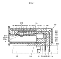
- a connector according to an embodiment of the present invention is described below with reference to Figs. 1 to 12 .
- a receptacle connector that is mountable on a circuit board 10 and is connectable with a plug connector compliant with USB 3.0 or USB 2.0 (not shown).
- the receptacle connector includes a body 100, a USB 3.0 contact group 200, a USB 2.0 contact group 300, a shell 400 for covering the body 100, and a spacer 500 adapted to be attached to the body 100.
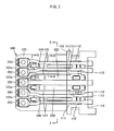
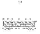
- a body 100 As shown in Figs. 1 to 3 , the receptacle connector includes a body 100, a USB 3.0 contact group 200, a USB 2.0 contact group 300, a shell 400 for covering the body 100, and a spacer 500 adapted to be attached to the body 100.
- a spacer 500 adapted to be attached to the body 100.
- the body 100 is a molded article produced by injection molding a general-purpose insulative synthetic resin such as a PBT (polybutylene terephthalate) or a PPS (polyphenylene sulfide). As shown in Figs. 1 to Fig. 7 , the body 100 includes a generally cuboid body main portion 110, and a plate-like protrusion 120 that projects from a front upper portion of the body main portion 110.
- a general-purpose insulative synthetic resin such as a PBT (polybutylene terephthalate) or a PPS (polyphenylene sulfide).
- PBT polybutylene terephthalate
- PPS polyphenylene sulfide
- a TX+ signaling contact 210 embedded in the upper portions of the body main portion 110 and the protrusion 120 are a TX+ signaling contact 210, a TX- signaling contact 220, a ground contact 230, an RX+ signaling contact 240, and an RX- signaling contact 250 (to be described later) of the USB 3.0 contact group 200 so as to be spaced apart from one another in the width direction of the body 100.
- the TX+ signaling contact 210, the TX- signaling contact 220, the ground contact 230, the RX+ signaling contact 240, and the RX- signaling contact 250 are disposed corresponding to the positions of the USB 3.0 plug contacts of the USB 3.0 plug.
- the front central portion of the body main portion 110 has four front recesses 111 of generally rectangular shape as shown in Figs. 1 , 2 , and 7 , at corresponding positions to the positions of the USB 2.0 plug contacts of the USB 2.0 plug. Above the front recesses 111 of the body main portion 110, there are four press-fitting holes 112 that communicate with the respective front recesses 111.
- the press-fitting holes 112 press-fittingly receive press fitting portions 311, 321, 331, and 341 of a Vbus contact 310, a Data- contact 320, a Data+ contact 330, and a GND contact 340 (to be described later) of the USB 2.0 contact group 300.
- the Vbus contact 310, the Data- contact 320, the Data+ contact 330, and the GND contact 340 received in the press-fitting holes 112 are led out at their elastic deformation portions 312, 322, 332, and 342 (to be described later) from the front recesses 111.
- recesses 121 of generally rectangular parallelepiped shape at the lower end of the protrusion 120.
- the longitudinal ends of the recesses 121 communicate with the respective front recesses 111.
- the recesses 121 respectively receive portions led out from the front recesses 111 of the Vbus contact 310, the Data- contact 320, the Data+ contact 330, and the GND contact 340 of the USB 2.0 contact group 300--more particularly, the elastic deformation portions 312, 322, 332, and 342 and movable contact portions 313, 323, 333, and 343 (to be described later).
- each of the recesses 121 is provided in its inner wall on the other longitudinal end with a guide hole 121a that extends vertically.
- the guide holes 121a receive and guide leading end portions 313a, 323a, 333a, and 343a of the movable contact portions 313, 323, 333, and 343 in a vertically movable manner.
- the lower edges of the guide holes 121a are in contact with the leading end portions 313a, 323a, 333a, and 343a so as to function as retaining portions 121b for retaining the Vbus contact 310, the Data- contact 320, the Data+ contact 330, and the GND contact 340 in a preload state.
- the body main portion 110 is provided in its rear central portion with a rear recess 113 that communicates with the four press-fitting holes 112.
- the Vbus contact 310 the Data- contact 320, the Data+ contact 330, and the GND contact 340 of the USB 2.0 contact group 300 that are partly press-fitted into the press-fitting holes 112, their lead-out portions 314, 324, 334, and 344 (to be described later) are led out of the body 100 through the rear recess 113.
- the TX+ signaling contact 210 In the TX+ signaling contact 210, the TX- signaling contact 220, the ground contact 230, the RX+ signaling contact 240, and the RX- signaling contact 250 of the USB 3.0 contact group 200 that are embedded in the upper portions of the body main portion 110 and the protrusion 120, their lead-out portions 213, 223, 233, 243, and 253 (to be described later) are also led out of the body 100 through the rear recess 113. As shown in Fig. 1 , the rear recess 113 fittingly receives a perpendicular portion 510 of the substantially plate-like spacer 500 of a generally L-shape in side view.
- the shell 400 is a rectangular tubular member made of metal. As shown in Fig. 1 , the shell 400 has a shell main portion 410 and a cover 420 that is continuous from the upper portion of the rear end of the shell main portion 410.
- the shell main portion 410 covers the outer periphery of the body 100. There is accordingly formed a plug insertion space ⁇ between the protrusion 120 of the body 100 and the lower end of the shell main portion 410.
- the plug insertion space ⁇ is adapted to receive a USB 3.0 plug or a USB 2.0 plug.
- Opposite ends of the shell main portion 410 are provided with paired connecting pieces 411 (only one of which being shown in Fig. 1 ) to be connected to a ground line on the circuit board 10.
- the cover 420 is bent substantially perpendicularly to the shell main portion 410 so as to cover the rear end surface of the spacer 500 that is attached to the body 100.
- the spacer 500 is a molded article in a generally L shape in cross-section, produced by injection molding a general-purpose insulative synthetic resin similar to that of the body 100.
- This spacer 500 has the perpendicular portion 510 and a base portion 520 disposed perpendicularly to the perpendicular portion 510.
- the perpendicular portion 510 has five through holes 511 for passing therethrough the lead-out portions 213, 223, 233, 243, and 253 of the TX+ signaling contact 210, the TX- signaling contact 220, the ground contact 230, the RX+ signaling contact 240, and the RX- signaling contact 250 of the USB 3.0 contact group 200.
- the base portion 520 is a plate-like member to be placed on the circuit board 10.
- the base portion 520 has four through holes 521 for passing therethrough connecting portions 315, 325, 335, and 345 (to be described later) of the Vbus contact 310, the Data- contact 320, the Data+ contact 330, and the GND contact 340 in the USB 2.0 contact group 300.
- the base portion 520 is also provided with paired locking arms to be locked at the two ends of the body 100.
- the USB 3.0 contact group 200 includes the TX+ signaling contact 210 (one of a pair of first contacts for differential signaling), the TX- signaling contact 220 (the other of the pair of first contacts), the ground contact 230, the RX+ signaling contact 240 (one of a pair first contacts for differential signaling), and the RX- signaling contact 250 (the other of the pair of first contacts).
- the TX+ signaling contact 210 is a conductive terminal of a substantially L shape in cross section, as shown in Figs. 9 , 10 , and 11A .
- the TX+ signaling contact 210 has a plate-like main portion 211, a contact portion 212 continuous from the leading end of the main portion 211, the substantially L-shaped lead-out portion 213 continuous from the rear end of the main portion 211, and a plate-like connecting portion 214 continuous from the rear end of the lead-out portion 213.
- the main portion 211 is embedded in the body 100 by insert molding above the front recess 111 and the recess 121 of the body 100.
- the main portion 211 has a leading end portion 211a bent widthwise and a rear end portion 211b.
- the contact portion 212 is a plate-like member that is bent substantially in a U shape in cross section and is wider than the main portion 211.
- the contact portion 212 is embedded by insert molding in the leading end of the protrusion 120.
- the contact portion 212 has a lower face exposed from a cutout that is provided at the lower edge of the leading end of the protrusion 120 so as to be contactable with a USB 3.0 plug contact.
- the lead-out portion 213 of a generally L shape in cross section is led out from the rear recess 113.
- the perpendicular portion of the lead-out portion 213 is adapted to pass through an associated through hole 511 in the perpendicular portion 510 of the spacer 500.
- the connecting portion 214 projects downward from the spacer 500. It is electrically connectable with a signal line on the circuit board 10 by soldering or other means.
- the TX- signaling contact 220 has a substantially same configuration with that of the TX+ signaling contact 210, except that a leading end portion 221a of a main portion 221 is bent oppositely with respect to the leading end portion 211a of the main portion 211 of the contact 210. Therefore, the portions other than the leading end portion 221a will not be repeatedly described in detail.
- the pitch distance between the leading end portion 221a and the leading end portion 211a is larger than the pitch distance between the rear end portion 221b of the contact 220 and the rear end portion 211b. Accordingly, the leading end portion 211a of the main portion 211 has a higher impedance than the rear end portion 211b, resulting in an impedance mismatch between the leading end portion 211a and the rear end portion 211b.
- the leading end portion 221a of the main portion 221 has a higher impedance than the rear end portion 221b, resulting in an impedance mismatch between the leading end portion 221a and the rear end portion 221b. Consequently, there exists an impedance mismatch between the TX+ signaling contact 210 and the TX- signaling contact 220.
- each of the leading end portion 211a and the leading end portion 221a as a "second portion”
- each of the rear end portion 211b and the rear end portion 221b as "a first portion.”
- the RX+ signaling contact 240 is a mirror image version of the TX- signaling contact 220.
- the RX- signaling contact 250 is a mirror image version of the TX+ signaling contact 210. Accordingly, the RX+ signaling contact 240 or the RX- signaling contact 250 will not be repeatedly described in detail.
- the ground contact 230 has a similar configuration to the TX+ signaling contact 210 etc., except that its main portion 231 is not bent but a straight plate-like member. There will accordingly be no detailed description of the ground contact 230.
- the USB 2.0 contact group 300 as shown in Figs. 2 , 3 , and 9 includes the Vbus contact 310 (second contact), the Data- contact 320, the Data+ contact 330, and the GND contact 340 (second contact).
- the Vbus contact 310 is a conductive terminal of a generally L shape in cross section and is smaller than the TX+ signaling contact 210 and the like. As shown in Figs. 9 , 10 , and 12 , the Vbus contact 310 has the press fitting portion 311, the elastic deformation portion 312 continuous from the leading end of the press fitting portion 311, the movable contact portion 313 continuous from the leading end of the elastic deformation portion 312, the lead-out portion 314 continuous from the rear end of the press fitting portion 311, and the connecting portion 315 continuous from the rear end of the lead-out portion 314.
- the press fitting portion 311 has paired projections at the widthwise opposite ends.
- the press fitting portion 311 inclusive of these projections is slightly larger in width than the press fitting hole 112 in the body 100.
- the press fitting portion 311 is accordingly inserted into the press fitting hole 112 in the body 100 and is retained by the body 100.
- the Vbus contact 310 is disposed below and between the TX+ signaling contact 210 and the TX- signaling contact 220, but located offset toward the TX+ signaling contact 210, as shown in Figs. 2 and 9 .
- This arrangement of the contacts causes a difference in impedance between the TX+ signaling contact 210 and the TX- signaling contact 220.
- the movable contact portion 313 is a plate-like member in a generally V shape in cross section and with a smaller width than that of the elastic deformation portion 312.
- the leading end portion 313a of the movable contact portion 313 extends in a tongue shape.
- the elastic deformation portion 312 is a generally rectangular plate-like member that is inclined downward and is elastically deformable in the vertical direction.
- the elastic deformation portion 312 is received in the front recess 111 and the recess 121 of the body 100 and the movable contact portion 313 is received in the recess 121 of the body 100.
- the leading end portion 313a of the movable contact portion 313 is received in the guide hole 121a in the recess 121 so as to be brought into contact with the retaining portion 121b of the guide hole 121a.
- the elastic deformation portion 312 is elastically deformed slightly upward.
- the Vbus contact 310 is thus locked by the retaining portion 121b in the preload state, and the apex of the movable contact portion 313 projects downward from the recess 121.
- the leading end portion 313a is guided by the guide hole 121a and displaced from a contact position as shown in Fig. 5A to an insertion position as shown in Fig. 5B .
- the leading end portion 313a is in contact with the retaining portion 121b.
- the leading end portion 313a is inserted between the leading end portion 211a of the main portion 211 of the TX+ signaling contact 210 and the leading end portion 221a of the main portion 221 of the TX- signaling contact 220.
- the distance between the leading end portion 313a at the insertion position and the leading end portion 211a is smaller than the distance between an end portion 312a (to be described later) of the elastic deformation portion 312 and the rear end portion 211b of the main portion 211 of the TX+ signaling contact 210 as shown in Fig. 4b .
- the distance between the leading end portion 313a at the insertion position and the leading end portion 221a is smaller than the distance between an end portion 312b (to be described later) of the elastic deformation portion 312 and the rear end portion 221b of the main portion 221 of the TX- signaling contact 220 as shown in Fig. 4B .
- the leading end portion 313a when the leading end portion 313a is displaced from the contact position to the insertion position and is inserted between the leading end portion 211a and the leading end portion 221a, the leading end portions 211a and 221a each increase in capacitance and decrease in impedance. Therefore, impedances are matched between the leading end portion 211a and the rear end portion 211b of the main portion 211 of the TX+ signaling contact 210, and between the leading end portion 221a and the rear end portion 221b of the main portion 221 of the TX- signaling contact 220. That is, the leading end portion 313a functions as an adjusting portion as defined in the claims.
- leading end portion 211a and the leading end portion 221a are at a substantially equal distance to the leading end portion 313a at the insertion position. Therefore, the leading end portions 211a and 221a equally increase in capacitance and decrease in impedance. Further, the pitch distance between the leading end portions 211a and 221a is larger than the pitch distance between the rear end portions 211b and 221b, preventing the leading end portions 221a and 211a from interfering with the leading end portion 313a at the insertion position.
- the widthwise end portions 312a and 312b of the elastic deformation portion 312 are disposed so as to overlap in plane position with the rear end portion 211b of the main portion 211 of the TX+ signaling contact 210 and the rear end portion 221b of the main portion 221 of the TX- signaling contact 220, respectively.
- widthwise end portions 312a and 312b are adjacent to and overlapped in plane position with the rear end portion 211b of the main portion 211 of the TX+ signaling contact 210 and the rear end portion 221b of the main portion 221 of the TX- signaling contact 220, respectively.
- the widthwise end portions 312a and 312b serve as "adjacent portions” and also as “first and second overlapping portions” of the second contact as defined in the claims.
- the area of the end portion 312a overlapping the rear end portion 211b of the TX+ signaling contact 210 and the area of the end portion 312b overlapping the rear end portion 221b of the TX- signaling contact 220 are adjusted in accordance with the difference in impedance between the TX+ signaling contact 210 and the TX- signaling contact 220.
- the end portion 312b closer to the TX- signaling contact 220 is extended in the width direction so as to substantially equalize the area of the end portion 312a overlapping the rear end portion 211b of the TX+ signaling contact 210 and the area of the end portion 312b overlapping the rear end portion 221b of the TX- signaling contact 220.
- the elastic deformation portion 312 is designed to have such a width and shape that the impedance of the TX+ signaling contact 210 is substantially equalized to the impedance of the TX- signaling contact 220.
- the press fitting portion 311 and the lead-out portion 314 are each set to have a width in accordance with the width of the elastic deformation portion 312.
- the above configuration thus corrects impedance mismatch between the TX+ signaling contact 210 and the TX- signaling contact 220 due to the offset placement of the Vbus contact 310 toward the TX+ signaling contact 210.
- a long opening 312c (resilience suppressor) in an intermediate portion between the end portions 312a and 312b of the elastic deformation portion 312.
- the opening 312c suppresses increase in resilience of the Vbus contact 310 due to extension of the end portion 312a of the Vbus contact 310.
- the opening 312c can suppress increase in the contact pressure of the Vbus contact 310 to be exerted on a USB 2.0 plug contact, so that the contact pressure of the Vbus contact 310 can be set at a predetermined value that allows suitable electrical connection with a USB 2.0 plug contact.
- the lead-out portion 314 is a plate-like member of a generally L shape in cross section as shown in Figs 1 , 10 , and 12 .
- the lead-out portion 314 projects rearward from the body 100.
- the connecting portion 315 is a straight plate-like member as shown in Figs. 1 , 10 , and 12 .
- the connecting portion 315 is allowed to pass through an associated through hole 521 in the base portion 520 of the spacer 500 and is electrically connectable by soldering or other means to a signal line on the circuit board 10.
- the GND contact 340 has a mirror image version of the Vbus contact 310, except that widthwise end portions 342a and 342b are overlapped in plane position with the RX- signaling contact 250 and the RX+ signaling contact 240. No further description is provided on the GND contact 340.
- the Data- contact 320 is a conductive terminal of a generally L shape in cross section.
- the Data- contact 320 has the press fitting portion 321, the elastic deformation portion 322 continuous from the leading end portion of the press fitting portion 321, the movable contact portion 323 continuous from the leading end portion of the elastic deformation portion 322, the lead-out portion 324 continuous from the rear end of the press fitting portion 321, and the connecting portion 325 continuous from the rear end of the lead-out portion 324.
- the press fitting portion 321 is substantially the same as the press fitting portion 311 except that the press fitting portion 321 is smaller in width than the press fitting portion 311.
- the Data- contact 320 is disposed below the ground contact 230 on the left side in Fig. 9 .
- the movable contact portion 323 is a plate-like member of a substantially V shape in cross section.
- the elastic deformation portion 322 is configured the same as the elastic deformation portion 312, except that the elastic deformation portion 322 is of an equal width to the movable contact portion 323 and has no opening 312c.
- the lead-out portion 324 and the connecting portion 325 are configured substantially the same, except their widths, as the lead-out portion 314 and the connecting portion 315.
- the Data+ contact 330 is the same type of contact as the Data- contact 320.
- the Data+ contact 330 is disposed below the ground contact 230 on the right side in Fig. 9 . Except that, the Data+ contact 330 is the same as the Data- contact 320, so that no further description will not be provided.
- the receptacle connector configured as described above is assembled in the following steps. First, the body 100 is attached to the shell main portion 410. In this state, the cover 420 is disposed in parallel with the top panel of the shell main portion 410.
- the movable contact portion 313 of the Vbus contact 310 is inserted into the associated front recess 111 from the rear side of the body 100.
- the movable contact portion 313 is then moved toward the leading end of the body 100, and the press fitting portion 311 of the Vbus contact 310 is pressed into the press fitting hole 112 in the body 100.
- the elastic deformation portion 312 of the Vbus contact 310 is inserted into the front recess 111 and the recess 121 of the body 100, and the movable contact portion 313 is inserted into the recess 121 of the body 100.
- the leading end portion 313a of the movable contact portion 313 is inserted into the guide hole 121a in the recess 121 and is brought into contact and engaged in the preload state with the retaining portion 121b of the guide hole 121a.
- the Vbus contact 310 is thus attached to the body 100.
- the Data- contact 320, the Data+ contact 330, and the GND contact 340 are attached to the body 100 similarly to the Vbus contact 310. Accordingly, the Vbus contact 310 is disposed at a plane position between the TX+ signaling contact 210 and the TX- signaling contact 220 and at a different height position from the TX+ signaling contact 210 and the TX- signaling contact 220.
- the Data- contact 320 and the Data+ contact 330 are disposed on opposite sides of a vertical position of the ground contact 230.
- the GND contact 340 is disposed at a plane position between the RX+ signaling contact 240 and the RX- signaling contact 250 and at a different height from the RX+ signaling contact 240 and the RX- signaling contact 250.
- the connecting portions 214, 224, 234, 244, and 254 of the TX+ signaling contact 210, the TX- signaling contact 220, the ground contact 230, the RX+ signaling contact 240, and the RX- signaling contact 250 are inserted into the respective through holes 511 in the spacer 500.
- the connecting portions 315, 325, 335, and 345 of the Vbus contact 310, the Data- contact 320, the Data+ contact 330, and the GND contact 340 are inserted into the respective through holes 521 in the spacer 500.
- the spacer 500 is inserted into the rear recess 113 of the body 100.
- the lead-out portions 213, 223, 233, 243, and 253 of the TX+ signaling contact 210, the TX- signaling contact 220, the ground contact 230, the RX+ signaling contact 240, and the RX- signaling contact 250 are inserted into the through holes 511 in the spacer 500, and the connecting portions 214, 224, 234, 244, and 254 project downward out of the through holes 511.
- the lower ends of the connecting portions 315, 325, 335, and 345 of the Vbus contact 310, the Data- contact 320, the Data+ contact 330, and the GND contact 340 project downward out of the through holes 521 in the spacer 500.
- the cover 420 is bent substantially perpendicularly so as to cover the rear face of the spacer 500.
- the receptacle connector assembled as described above is mounted on the circuit board 10. More specifically, the connecting portions 214, 224, 244 and 254 of the TX+ signaling contact 210, the TX- signaling contact 220, the RX+ signaling contact 240, and the RX- signaling contact 250 are connected to signal lines on the circuit board 10, and the connecting portion 234 of the ground contact 230 is connected to a ground line on the circuit board 10. Also, the connecting portions 315, 325 and 335 of the Vbus contact 310, the Data- contact 320, and the Data+ contact 330 are connected to signal lines on the circuit board 10, and the connecting portion 345 of the GND contact 340 is connected to a ground line on the circuit board 10. Furthermore, the paired connecting pieces 411 of the shell 400 are connected to a ground line on the circuit board 10.
- the receptacle connector is thus mounted on the circuit board 10, and then it is connectable with a USB 3.0 plug or a USB 2.0 plug in the following manner.
- USB 3.0 plug contacts are brought into contact with the associated contact portions 212, 222, 232, 242 and 252 of the USB 3.0 contact group 200.
- the USB 3.0 plug presses the apexes of the movable contact portions 313, 323, 333 and 343 of the USB 2.0 contact group 300, so that the movable contact portions 313, 323, 333 and 343 as well as the elastic deformation portions 312, 322, 332 and 342 are elastically deformed upward inside the front recess 111 and the recess 121 of the body 100.
- the leading end portion 313a of the movable contact portion 313 is guided by the guide hole 121a in the body 100 and displaced from the contact position as shown in Fig. 5A to the insertion position as shown in Fig. 5B . Then, the leading end portion 313a is inserted between the leading end portion 211a of the TX+ signaling contact 210 and the leading end portion 221a of the TX- signaling contact 220, thereby being brought closer to the leading end portion 211a of the TX+ signaling contact 210 and the leading end portion 221a of the TX- signaling contact 220.
- the distance between the leading end portion 313a and the leading end portion 211a becomes smaller than the distance between the end portion 312a of the elastic deformation portion 312 and the rear end portion 211b as shown in Fig. 4B
- the distance between the leading end portion 313a and the leading end portion 221a becomes smaller than the distance between the end portion 312b of the elastic deformation portion 312 and the rear end portion 221b as shown in Fig. 4B
- the leading end portions 211a and 221a increase in capacitances and decrease in impedances. Consequently, impedances are matched between the leading end portion 211a and the rear end portion 211b and between the leading end portion 221a and the rear end portion 221b.
- the leading end portion 313a at the insertion position is at the equal distance from the leading end portion 211a and leading end portion 221a, so that the leading end portions 211a and 221a equally increase in capacitance and equally decrease in impedance.
- the leading end portion 343a of the movable contact portion 343 is guided by the guide hole 121a in the body 100 and displaced from the contact position to the insertion position.
- the leading end portion 343a is then inserted between the leading end portion 241a of the RX+ signaling contact 240 and the leading end portion 251a of the RX- signaling contact 250.
- the distance between the leading end portion 343a and the leading end portion 241a becomes smaller than the distance between the end portion 342b of the elastic deformation portion 342 and the rear end portion 241b.
- the distance between the leading end portion 343a and the leading end portion 251a becomes smaller than the distance between the end portion 342a of the elastic deformation portion 342 and the rear end portion 251b. Accordingly, the leading end portions 241a and 251a increase in capacitance and decrease in impedance. As a result, impedances are matched between the leading end portion 241a and the rear end portion 241b as well as between the leading end portion 251a and the rear end portion 251b.
- the leading end portion 343a at the insertion position is at the equal distance from the leading end portions 241a and 251a, so that the leading end portions 241a and leading end portion 251a equally increase in capacitance and equally decrease in impedance.
- the leading end portion 323a of the movable contact portion 323 and the leading end portion 333a of the movable contact portion 333 are guided by the guide holes 121a in the body 100 and displaced upward.
- the movable contact portions 323 and 333 and the elastic deformation portions 322 and 332 become substantially in parallel with the main portion 231 of the ground contact 230.
- the apexes of the movable contact portions 313, 323, 333 and 343 of the USB 2.0 contact group 300 are brought into contact with and are pressed by the respective USB 2.0 plug contacts. Accordingly, the movable contact portions 313, 323, 333 and 343 as well as the elastic deformation portions 312, 322, 332 and 342 are elastically deformed upward inside the front recess 111 and the recess 121 of the body 100.
- the leading end portion 313a of the movable contact portion 313 is guided by the guide hole 121a in the body 100 and displaced from the contact position as shown in Fig. 5A to the insertion position as shown in Fig. 5B .
- the leading end portion 313a is then inserted between the leading end portion 211a of the TX+ signaling contact 210 and the leading end portion 211a of the TX- signaling contact 220.
- leading end portion 343a of the movable contact portion 343 is guided by the guide hole 121a in the body 100 and displaced from the contact position to the insertion position.
- the leading end portion 343a is then inserted between the leading end portion 241a of the RX+ signaling contact 240 and the leading end portion 251a of the RX- signaling contact 250.
- the leading end portion 323a of the movable contact portion 323 and the leading end portion 333a of the movable contact portion 333 are guided by the guide holes 121a in the body 100 and displaced upward.
- the movable contact portions 323 and 333 and the elastic deformation portions 322 and 332 are brought into substantially parallel relation to the main portion 231 of the ground contact 230.
- the elastic deformation portion 312 of the Vbus contact 310 and the elastic deformation portion 342 of the GND contact 340 are elastically deformed upward. Accordingly, the leading end portion 313a of the movable contact portion 313 of the Vbus contact 310 and the leading end portion 343a of the movable contact portion 343 of the GND contact 340 are displaced from the contact positions to the insertion positions.
- leading end portion 313a is then inserted between the leading end portion 211a of the TX+ signaling contact 210 and the leading end portion 221a of the TX- signaling contact 220, while the leading end portion 343a is inserted between the leading end portion 241a of the RX+ signaling contact 240 and the leading end portion 251a of the RX- signaling contact 250.
- the distance between the leading end portion 313a and the leading end portion 211a is smaller than the distance between the end portion 312a of the elastic deformation portion 312 and the rear end portion 211b of the main portion 211 of the TX+ signaling contact 210, and the distance between the leading end portion 313a and the leading end portion 221a is also smaller than the distance between the end portion 312b of the elastic deformation portion 312 and the rear end portion 221b of the main portion 221 of the TX- signaling contact 220.
- the distance between the leading end portion 343a and the leading end portion 241a is smaller than the distance between the end portion 342b of the elastic deformation portion 342 and the rear end portion 241b of the main portion 241 of the RX+ signaling contact 240, and the distance between the leading end portion 343a and the leading end portion 251a is smaller than the distance between the end portion 342a of the elastic deformation portion 342 and the rear end portion 251b of the RX- signaling contact 250. Therefore, the leading end portions 211a, 221a, 241a, and 251a each increase in capacitance and decrease in impedance.
- the Vbus contact 310 of the USB 2.0 standard is advantageously used to match impedances between the leading end portion 211a and the rear end portion 211b of the main portion 211 of the TX+ signaling contact 210 and between the leading end portion 221a and the rear end portion 221b of the main portion 221 of the TX- signaling contact 220.
- the GND contact 340 is used to match impedances between the leading end portion 241a and the rear end portion 241b of the RX+ signaling contact 240 and between the leading end portion 251a and the rear end portion 251b of the RX- signaling contact 250.
- impedances are matched between the TX+ signaling contact 210 and the TX- signaling contact 220 and between the RX+ signaling contact 240 and the RX- signaling contact 250.
- the end portion 312b is extended in the width direction, so that the area of the end portion 312a overlapping the rear end portion 211b of the main portion 211 of the TX+ signaling contact 210 is substantially equalized to the area of the end portion 312b overlapping the rear end portion 221b of the main portion 221 of the TX- signaling contact 220.
- the end portion 342b is extended in the width direction, so that the area of the end portion 342b overlapping the rear end portion 241b of the main portion 241 of the RX+ signaling contact 240 is substantially equalized to the area of the end portion 342a overlapping the rear end portion 251b of the main portion 251 of the RX- signaling contact 250.
- the Vbus contact 310 is disposed offset toward the TX+ signaling contact 210 and the GND contact 340 is disposed offset toward the RX- signaling contact 250 to comply with the USB 2.0 standard, impedances can be matched between the TX+ signaling contact 210 and the TX- signaling contact 220 and between the RX+ signaling contact 240 and the RX- signaling contact 250.
- the Vbus contact 310 and the GND contact 340 of the USB 2.0 standard are utilized to match impedances between the TX+ signaling contact 210 and the TX- signaling contact 220 and between the RX+ signaling contact 240 and the RX- signaling contact 250.
- the Vbus contact 310 of the USB 2.0 standard is utilized to match impedances between the leading end portion 211a and the rear end portion 211b of the main portion 211 of the TX+ signaling contact 210 and between the leading end portion 221a and the rear end portion 221b of the main portion 221 of the TX- signaling contact 220, and also to match impedances between the TX+ signaling contact 210 and the TX- signaling contact 220.
- the GND contact 340 of the USB 2.0 standard is utilized to match impedances between the leading end portion 241a and the rear end portion 241b of the RX+ signaling contact 240 and between the leading end portion 251a and the rear end portion 251b of the RX- signaling contact 250, and also to match impedances between the RX+ signaling contact 240 and the RX- signaling contact 250.
- the connector with such a simplified configuration can be manufactured at reduced cost.
- the Vbus contact 310 is provided with the opening 312c in the intermediate portion between the end portion 312a and the end portion 312b of the elastic deformation portion 312, so that the opening 312c serves to reduce the resilience of the Vbus contact 310 that should have increased due to the extension of the end portion 312b.
- the GND contact 340 is provided with the opening 342c in the intermediate portion between the end portion 342a and the end portion 342b of the elastic deformation portion 342, so that the opening 342c serves to reduce the resilience of the GND contact 340 that should have increased due to the extension of the end portion 342b.
- Another advantage of the above-described connector is the ease of the impedance adjustment between the TX+ signaling contact 210 and the TX- signaling contact 220. More particularly, the areas of the end portions 312a and 312b overlapping the TX+ signaling contact 210 and the TX- signaling contact 220, respectively, can be adjusted by changing the size and/or the shape of the opening 312c. Similarly, the impedances can be easily adjusted between the RX+ signaling contact 240 and the RX- signaling contact 250, by changing the size and/or the shape of the opening 342c.
- the provision of the opening 312c in the intermediate portion reduces the areas of the end portion 312a and 312b overlapping the TX+ signaling contact 210 and the TX- signaling contact 220, respectively. Also, the provision of the opening 342c in the intermediate portion reduces the areas of the end portions 342b and 342a overlapping the RX+ signaling contact 240 and the RX- signaling contact 250, respectively. It is thus possible to reduce impedances of the TX+ signaling contact 210, the TX- signaling contact 220, the RX+ signaling contact 240, and the RX- signaling contact 250.
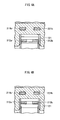
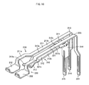
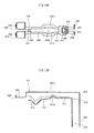
- Figs 13A and 13B are schematic views of a design variation of the TX+ signaling contact, the TX- signaling contact, and the Vbus contact of the connector, in which Fig. 13A is a bottom view and Fig. 13B is a cross-sectional view.
- Figs. 14A and 14B are schematic views of another design variation of the TX+ signaling contact, the TX- signaling contact, and the Vbus contact of the connector, in which Fig. 14A is a bottom view and Fig. 14B is a cross-sectional view.
- Figs. 14A is a bottom view
- Fig. 14B is a cross-sectional view.
- FIGS. 15A to 15C are schematic bottom views of a design variation of the Vbus contact of the connector, in which Fig. 15A shows a configuration with no opening provided therein, Fig. 15B shows a configuration with a bent intermediate portion of an elastic deformation portion, and Fig. 15C shows a configuration with semicircular overlapping portions provided at ends of the elastic deformation portion.
- the design of the body 100 can be modified in any manner as long as it can retain at least one first contact and a second contact that is disposed at a different height from that of the at least one first contact.
- the shapes and locations of the contacts of the USB 3.0 contact group 200 are not limited to the ones of the above embodiment but can be modified.
- the USB 3.0 contact group 200 according to the above embodiment is compliant with the USB 3.0 standard, but it is not limited thereto but may be adaptable to a different standard.
- the contacts of the USB 3.0 contact group 200 may be or may not be embedded in the body 100.
- the contacts may be press-fitted into holes made in the body 100, in a similar manner as the Vbus contact 310 and other contacts that are press-fitted.
- leading end portion 313a is inserted between the leading end portion 211a of the TX+ signaling contact 210 and the leading end portion 221a of the TX- signaling contact 220, and the leading end portion 343a is inserted between the leading end portion 241a of the RX+ signaling contact 240 and the leading end portion 251a of the RX- signaling contact 250.
- leading end portion 313a has only to be brought closer to the leading end portion 211a of the TX+ signaling contact 210 and to the leading end portion 221a of the TX- signaling contact 220, and the leading end portion 343a has only to be brought closer to the leading end portion 241a of the RX+ signaling contact 240 and to the leading end portion 251a of the RX- signaling contact 250.
- impedances can be matched between the leading end portion 211a and the rear end portion 211b of the main portion 211 of the TX+ signaling contact 210, between the leading end portion 221a and the rear end portion 221b of the main portion 221 of the TX- signaling contact 220, between the leading end portion 241a and the rear end portion 241b of the RX+ signaling contact 240, and between the leading end portion 251a and the rear end portion 251b of the RX- signaling contact 250.
- the distance between the leading end portion 313a and the leading end portion 211a is smaller than the distance between the end portion 312a of the elastic deformation portion 312 and the rear end portion 211b of the TX+ signaling contact 210, and the distance between the leading end portion 313a and the leading end portion 221a is smaller than the distance between the end portion 312b of the elastic deformation portion 312 and the rear end portion 221b of the TX- signaling contact 220.
- the present invention is not limited to these distance relations. The distance relations depend on the pitch distance between the leading end portion 211a and the leading end portion 221a and the shapes thereof.
- the distance between the leading end portion 313a and the leading end portion 211a may be substantially equal to or larger than the distance between the end portion 312a of the elastic deformation portion 312 and the rear end portion 211b of the TX+ signaling contact 210, and the distance between the leading end portion 313a and the leading end portion 221a may be substantially equal to or larger than the distance between the end portion 312b of the elastic deformation portion 312 and the rear end portion 221b of the TX- signaling contact 220.
- impedances can be matched between the leading end portion 211a and the rear end portion 211b of the main portion 211 of the TX+ signaling contact 210 and between the leading end portion 221a and the rear end portion 221b of the main portion 221 of the TX- signaling contact 220, because the leading end portion 313a is brought closer to the leading end portion 211a of the TX+ signaling contact 210 and to the leading end portion 221a of the TX- signaling contact 220.
- the leading end portion 313a at the insertion position is equally distanced from the leading end portion 211a and the leading end portion 221a.
- the present invention is not limited thereto.
- the distance between the leading end portion 313a and the leading end portion 211a is not required to be substantially equal to the distance between the leading end portion 313a and the leading end portion 221a at the insertion position.
- the leading end portion 313a is only brought closer to the leading end portion 211a and the leading end portion 221a.
- leading end portion 211a of the main portion 211 and the leading end portion 221a of the main portion 221 act as the second portions with different impedances from the rear end portion 211b of the main portion 211 and the rear end portion 221b of the main portion 221, respectively.
- the present invention is not limited thereto. For example, in a case as shown in Fig.
- the intermediate portion of the elastic deformation portion 312 of the Vbus contact 310 may be provided with a bent portion 312d, which can be brought close to the intermediate portions 211c and 221c in accordance with elastic deformation of the elastic deformation portion 312, as shown in Fig. 13B .
- the bent portion 312d functions as the adjusting portion.
- the "first portion” defined in the claims is not limited to the portion other than the second portion of the main portion, but is to be appropriately determined in relation to the second portion.
- the leading ends 211a and 221a act as the second portions due to the larger pitch distance between the leading end portion 211a and the leading end portion 221a than the pitch distance between the rear end portion 211b and the rear end portion 221b.
- the present invention is not limited to the above case.
- the leading end portions 211a and 221a may act as the second portions due to a difference in shape, such as width or thickness, of the leading end portions 211a and 221a from the rear end portions 211b and 221b. This modification is also applicable to the above case where portions other than the leading end portions 211a and 221a act as the second portions.
- leading end portions 211a and 221a may act as the second portions due to a smaller pitch distance between the leading end portion 211a and the leading end portion 221a than the pitch distance between the rear end portion 211b and the rear end portion 221b.
- the leading end portions 211a and 221a may be lower in impedance than the rear end portions 211b and 221b. In this case, as shown in Figs.
- the TX+ signaling contact 210 and the TX- signaling contact 220 can elastically deform in a direction away from the Vbus contact 310, and the leading end portion 211a of the main portion 211 of the TX+ signaling contact 210 and the leading end portion 221a of the main portion 221 of the TX- signaling contact 220 are displaced in a direction away from the leading end portion 313a of the Vbus contact 310. Such displacements reduce the capacitances and increase the impedances of the leading end portions 211a and 221a.
- the Vbus contact 310 of the USB 2.0 standard can be used to match impedances between the leading end portion 211a and the rear end portion 211b of the main portion 211 of the TX+ signaling contact 210 and between the leading end portion 221a and the rear end portion 221b of the main portion 221 of the TX- signaling contact 220.
- the Vbus contact 310 may elastically deform in a direction away from the TX+ signaling contact 210 and the TX- signaling contact 220, and the leading end portion 313a of the Vbus contact 310 may be displaced in a direction away from the leading end portion 211a of the main portion 211 of the TX+ signaling contact 210 and from the leading end portion 221a of the main portion 221 of the TX- signaling contact 220.
- This modification is similarly applicable to the above case where portions other than the leading end portions 211a and 221a act as the second portion.
- the Vbus contact 310, the Data- contact 320, the Data+ contact 330, and the GND contact 340 are provided as movable terminals that are elastically deformable, and the TX+ signaling contact 210, the TX- signaling contact 220, the ground contact 230, the RX+ signaling contact 240, and the RX- signaling contact 250 are provided as fixed terminals that are embedded in the body 100.
- the Vbus contact 310, the Data- contact 320, the Data+ contact 330, and the GND contact 340 may be provided as fixed terminals and the TX+ signaling contact 210, the TX- signaling contact 220, the ground contact 230, the RX+ signaling contact 240, and the RX- signaling contact 250 may be provided as movable terminals.
- the TX+ signaling contact 210, the TX- signaling contact 220, the RX+ signaling contact 240, and the RX- signaling contact 250 may be elastically deformed by an inserted plug, so that the leading end portion 313a is brought relatively close to the leading end portion 211a of the TX+ signaling contact 210 and the leading end portion 221a of the TX- signaling contact 220, and the leading end portion 343a is brought relatively close to the leading end portion 241a of the RX+ signaling contact 240 and the leading end portion 251a of the RX- signaling contact 250.
- the TX+ signaling contact 210 and the TX- signaling contact 220 are a pair of differential signaling contacts and the RX+ signaling contact 240 and the RX- signaling contact 250 are another pair of differential signaling contacts.
- these contacts may be provided as other kinds of contacts than the differential signaling contacts.
- the present invention is applicable to a case where there is a difference in impedance between a portion (second portion) and another portion (first portion) of a single contact (first contact) due to the relation with adjacent contacts, the shapes thereof, or other reasons.
- a portion of the second contact disposed at a different height from the first contact is brought relatively close to or apart from the second portion by elastic deformation of the first or second contact, so that impedances can be matched between the second portion and the first portion of the first contact.
- the shapes and arrangement of the contacts of the USB 2.0 contact group 300 are not limited to the ones of the above embodiment but may be modified in design.
- the USB 2.0 contact group 300 is not limited to contacts compliant with the USB 2.0 standard, but may be applicable to contacts of a different standard.
- the above embodiment is described such that the area of the end portion 312a of the Vbus contact 310 overlapping the rear end portion 211b of the main portion 211 of the TX+ signaling contact 210 is substantially equal to the area of the end portion 312b of the Vbus contact 310 overlapping the rear end portion 221b of the main portion 221 of the TX- signaling contact 220, and such that the area of the end portion 342b of the GND contact 340 overlapping the rear end portion 241b of the main portion 241 of the RX+ signaling contact 240 is substantially equal to the area of the end portion 342a of the GND contact 340 overlapping the rear end portion 251b of the main portion 251 of the RX- signaling contact 250.
- the end portions 312a and 312b of the Vbus contact 310 are not required to overlap the TX+ signaling contact 210 and the TX- signaling contact 220, respectively, in plane position, and the end portions 342b and 342a of the GND contact 340 are not required to overlap the RX+ signaling contact 240 and the RX- signaling contact 250, respectively, in plane position.
- the area of the end portion 312a overlapping the rear end portion 211b of the TX+ signaling contact 210 and the area of the end portion 312b overlapping the rear end portion 221b of the TX- signaling contact 220 are not required to be made substantially equal to each other as described above but may be adjusted in accordance with the difference in impedance between the TX+ signaling contact 210 and the TX- signaling contact 220.
- the end portions 312a and 312b of the elastic deformation portion 312 overlap the rear end portion 211b of the main portion 211 of the TX+ signaling contact 210 and the rear end portion 221b of the main portion 221 of the TX- signaling contact 220, respectively, in plane position
- the end portions 342b and 342a of the elastic deformation portion 342 overlap the rear end portion 241b of the main portion 241 of the RX+ signaling contact 240 and the rear end portion 251b of the main portion 251 of the RX- signaling contact 250, respectively, in plane position.
- each end portion of the ground contact 230 may overlap the Vbus contact 310 and the GND contact 340 in plane position.
- FIG. 15A An example of such modification is a Vbus contact 310' as shown in Fig. 15A .
- the area of one end (first overlapping portion) overlapping a first differential signaling contact is made substantially equal to the area of the other end (second overlapping portion) overlapping a second differential signaling contact.
- Fig. 15A also illustrates a press fitting portion 311' and a movable contact portion 313' of the modified Vbus contact 310'.
- FIG. 15B Another example is a Vbus contact 310" as shown in Fig. 15B , wherein a connecting portion 312c" is provided to connect a leading end portion 312a" (first overlapping portion) of the elastic deformation portion 312" and a proximal end portion 312b" (second overlapping portion) of the elastic deformation portion 312".
- the connecting portion 312c" extends perpendicular to the leading end portion 312a" and to the proximal end 312b".
- the area of the leading end portion 312a" overlapping the first differential signaling contact may be made substantially equal to the area of the proximal end 312b" overlapping the second differential signaling contact, so that the first and second differential signaling contacts are matched in impedance.
- the connecting portion 312c" may extend at an angle to the leading end portion 312a" and the proximal end 312b".
- Fig. 15B also illustrates a press fitting portion 311" and a movable contact portion 313" of the modified Vbus contact 310".
- Still another modification example is a Vbus contact 310"' as shown in Fig. 15C , wherein the elastic deformation portion 312"' has semicircular overlapping portions 312a"' and 312b"' in its intermediate portion.
- the areas of the overlapping portions 312a"' and 312b"' overlapping the first and second differential signaling contacts are set to be substantially equal to each other, so that the first and second differential signaling contacts are matched in impedance.
- Fig. 15C also illustrates a press fitting portion 311"' and a movable contact portion 313"' of the modified Vbus contact 310"'.
- the Vbus contact 310 and the GND contact 340 are provided in the intermediate portions of the elastic deformation portions 312 and 342 with the openings 312c and 342c that function as the resilience suppressors.
- these resilience suppressors are optional.
- the resilience suppressors are not limited to such openings but may be modified in design as long as the resilience suppressors are capable of suppressing the resiliences of the second contacts such as the Vbus contact 310 and the GND contact 340, which resiliences should have increased due to the widthwise extension for the purpose of impedance matching.
- the resilience suppressors may be formed as cutouts provided at the opposite ends of the proximal ends of the elastic deformation portions 312 and 342, or may be formed as thin portions provided at the elastic deformation portions 312 and 342, or may be formed in any other manners.
- the connector described above is compliant with the two types of standards, namely, USB 2.0 and USB 3.0 standards.
- the connector of the invention is not limited to this but may be adaptable to different standards.
- the above connector is described as a socket or a receptacle connector, but the connector is applicable to a plug connector having contacts connected to a cable.
Landscapes
- Details Of Connecting Devices For Male And Female Coupling (AREA)
- Coupling Device And Connection With Printed Circuit (AREA)
Abstract
Description
- The present invention relates to connectors that are used mainly for high-speed digital signal transmission and are capable of providing favorable impedance matching.
- A known connector of this kind has pairs of differential contacts compliant with a new standard and contacts compliant with a conventional standard. In the pairs of differential contacts compliant with the new standard, the pitch distance between portions of the contacts in the vicinity of the contact portions, as well as the widths thereof, are different from those of other portions of the contacts. These differences cause differences in impedance between the portions in the vicinity of the contact portions and the other portions.
- A solution to this problem is to provide ground contacts near the portions in the vicinity of the contact portions so as to adjust the impedances between the portions in the vicinity of the contact portions of the differential pair contacts and the other portions (see Japanese Unexamined Patent Application Publication No.
2003-505826 - However, the provision of ground contacts near the portions in the vicinity of the contact portions of the differential pair contacts leads to an increase in the number of components and in the complexity of the entire configuration of the connector.
- The present invention has been made in view of the above circumstances. An embodiment of the invention provides a connector compliant with two standards and in a simple configuration with matched impedances in a contact.
- A connector according to the present invention includes an insulative body; and a first contact and a second contact that are disposed in the body at different height levels from each other, the first contact or the second contact being elastically deformable. The first contact includes a first portion and a second portion, the second portion having a higher impedance than that of the first portion. The second contact includes an adjusting portion to be brought close to the second portion by elastic deformation of the first contact or the second contact in a direction close to the second contact or the first contact.
- In the connector thus configured, when the first contact compliant with a first standard or the second contact compliant with a second standard is elastically deformed in the direction of close to the second contact or the first contact, the adjusting portion of the second contact is brought close to the second portion of the first contact. As a result, the second portion increases in capacitance and decreases in impedance. It is therefore possible to alleviate the impedance mismatch between the second portion and the first portion of the first contact without providing a ground contact as in the conventional art. Such connector has an advantageously simple configuration and can be manufactured at low cost.
- If the connector has a pair of first contacts for differential signaling, the second contact may be disposed between the first contacts in plane position.
- The second contact may further include an adjacent portion that is adjacent to the first portion of the first contact. In a state where the first contacts or the second contact is elastically deformed, a distance between each of the second portions and the adjusting portion may be smaller than a distance between each of the first portions of the first contacts and the adjacent portion of the second contact. In this case, the adjusting portion is brought to a smaller distance from each of the second portions relative to the distance between each of the first portions of the first contacts and the adjacent portion of the second contact, so that the second portions can further improve in impedance, resulting in matched impedances between the second portions and the first portions of the first contacts.
- If a pitch distance between the second portions of the paired first contacts is larger than a pitch distance between the first portions of the paired first contacts, in the state where the first contacts or the second contact is elastically deformed in the direction close to the second contact or the first contacts, the adjusting portion may be inserted between the second portions of the paired first contacts so as to be located at an equal distance from either of the second portions. The body may be provided with a retaining portion for allowing leading end portions of the first contacts or a leading end portion of the second contact to be in contact therewith in a preloaded state so as to prevent the first contacts or the second contact from elastically deforming in a direction away from the second contact or the first contacts.
- Even in the above case where the second portions of the paired first contacts have significantly higher impedances than the first portions due to the larger pitch distance therebetween than that between the first portions, impedances can be matched between the second portions and the first portions of the paired first contacts by inserting the adjusting portion between the second portions so that the adjusting portion is disposed at an equal distance from either of the second portions. Moreover, since the pitch distance between the second portions is larger than that between the first portions in the first contacts, the adjusting portion can be kept from interfering with the second portions when inserted therebetween.
- The body may be provided with a guide hole for receiving the leading end portion of one of the first and second contacts so as to be movable in a direction along elastic deformation of the one of the first and second contacts. In this case, as the guide hole guides the leading end portion of one of the first and second contacts, the one of the first and second contacts can elastically deforms accurately in the direction close to the other contact.
- The adjusting portion may be the leading end portion of the second contact.
- The second contact may be disposed offset toward one of the paired first contacts. The second contact may have a first overlapping portion overlapping one of the first contacts in plane position and a second overlapping portion overlapping the other first contact in plane position. Areas of the first and second overlapping portions overlapping the first contacts may be adjusted in accordance with a difference in impedance between the first contacts.
- In this case, the first contacts have matched impedances because the areas of the first and second overlapping portions of the second contact overlapping the paired first contacts are adjusted in accordance with the difference in impedance between the first contacts. In other words, the second contact of the second standard can be utilized not only to match impedances between the second portion and the first portion of each of the first contacts but also to match impedances between the first contacts. Such connector has an advantageously simple configuration and can be manufactured at low cost.
- The areas of the first and second overlapping portions overlapping the first contacts may be substantially equal to each other. In this case, the capacitances of the first contacts are made substantially equal to each other because of substantially equalized areas of the first and second overlapping portions overlapping the first contacts, thereby achieving matched impedance between the first contacts.
- If the first and second overlapping portions are located at widthwise opposite ends of the second contact, at least one of the first and second overlapping portions can be extended in the width direction. In this case, the areas of the first and second overlapping portions overlapping the first contacts can be made substantially equal to each other by extension in the width direction of the at least one of the first and second overlapping portions. In short, impedances can be easily matched between the first contacts by simply changing the width of the second contact.
- If the second contact is an elastically deformable terminal, the second contact may be provided with a resilience suppressor for suppressing increase in resilience of the second contact due to extension in the width direction of the at least one of the first and second overlapping portions. Providing the resilience suppressor can suppress increase in resilience of the second contact caused by extension in the width direction of at least one of the first and second overlapping portions. The resilience suppressor can thus suppress increase in contact pressure of the second contact due to increase in resilience of the second contact.
- The resilience suppressor may be an opening made in an intermediate portion between the first and second overlapping portions of the second contact. Providing the opening in the intermediate portion between the first and second overlapping portions of the second contact can favorably suppress increase in resilience of the second contact due to extension in the width direction of at least one of the first and second overlapping portions, and can accordingly suppress increase in contact pressure of the second contact. The second contact can thus be brought into contact with a target contact at a predetermined contact pressure. Another advantage is ease of impedance matching between the first contacts. More particularly, the areas of the first and second overlapping portions overlapping the first contacts can be adjusted by changing the shape and/or size of the opening. Still another advantage of providing the opening in the intermediate portion of the second contact is reduction of the areas of the first and second overlapping portions of the second contact overlapping the first contacts, resulting in reduction in impedance of the first contacts.
- Alternatively, the second contact may further be provided with a connecting portion for connecting the first overlapping portion on a leading side and the second overlapping portion on a proximal side, and the connecting portion extends perpendicularly or at an angle to the first and second overlapping portions. In this case, impedances can be easily matched between the first contacts by simply providing the connecting portion to connect between the first overlapping portion on the leading side and the second overlapping portion on the proximal side, which have substantially equal areas overlapping the respective first contacts.
- Another connector according to the present invention includes an insulative body; and a first contact and a second contact that are disposed in the body at different height levels from each other, the first contact or the second contact being elastically deformable. The first contact includes a first portion and a second portion having a lower impedance than that of the first portion. The second contact includes an adjusting portion adapted to be moved apart from the second portion by elastic deformation of the first contact or the second contact in a direction away from the second contact or the first contact.
- In the connector thus configured, when the first contact compliant with the first standard or the second contact compliant with the second standard is elastically deformed in the direction away from the second contact or the first contact, the adjusting portion of the second contact is brought away from the second portion of the first contact. As a result, the second portion decreases in capacitance and increases in impedance. It is therefore possible to alleviate the impedance mismatch between the second portion and the first portion of the first contact without providing a ground contact as in the conventional art. Such connector has an advantageously simple configuration and can be manufactured at low cost.
- The invention will now be described by way of example only and without limitation by reference to the drawings, in which:
-
Fig. 1 is a schematic cross-sectional view of a connector according to an embodiment of the present invention. -
Fig. 2 is a schematic plan view of the connector with a shell removed, illustrating the inside of the connector transparently. -
Fig. 3 is a diagrammatic cross-sectional view taken along line 3-3 inFig. 2 . -
Figs. 4A and 4B are diagrammatic cross-sectional views taken a portion of the connector along line 4-4 inFig. 2 , in whichFig. 4A shows a rear end portion of a main portion of a Vbus contact before elastic deformation, andFig. 4B shows the rear end portion of the main portion of the Vbus contact after elastic deformation. -
Figs. 5A and 5B are diagrammatic cross-sectional views taken a portion of the connector along line 5-5 inFig. 2 , in whichFig. 5A shows a leading end portion of the main portion of the Vbus contact before elastic deformation, andFig. 5B shows the leading end portion of the main portion of the Vbus contact after elastic deformation. -
Fig. 6 is a schematic perspective view of a body of the connector. -
Fig. 7 is a schematic bottom view illustrating the inside of the body of the connector transparently. -
Fig. 8 is a schematic perspective view of a spacer of the connector. -
Fig. 9 is a schematic bottom view showing the layout of the contacts of the connector. -
Fig. 10 is a schematic perspective view of a TX+ signaling contact, a TX- signaling contact, and the Vbus contact of the connector. -
Fig. 11A is a schematic perspective view of the TX+ signaling contact of the connector, andFig. 11B is a schematic perspective view of the TX- signaling contact thereof. -
Fig. 12 is a schematic perspective view of the Vbus contact of the connector. -
Figs 13A and 13B are schematic views of a design variation of the TX+ signaling contact, the TX- signaling contact, and the Vbus contact of the connector, in whichFig. 13A is a bottom view andFig. 13B is a cross-sectional view. -
Figs 14A and 14B are schematic views of another design variation of the TX+ signaling contact, the TX- signaling contact, and the Vbus contact of the connector, in whichFig. 14A is a bottom view andFig. 14B is a cross-sectional view. -
Figs. 15A to 15C are schematic bottom views of design variations of the Vbus contact of the connector, in whichFig. 15A shows a configuration with no opening provided therein,Fig. 15B shows a configuration with a bent intermediate portion of an elastic deformation portion, andFig. 15C shows a configuration with semicircular overlapping portions provided at ends of the elastic deformation portion. - In the description which follows, relative spatial terms such as "upper", "lower", "upward", "downward", "to", "bottom", "above", "below", "front", "rear", etc., are used for the convenience of the skilled reader and refer to the orientation of the connector and its constituent parts as depicted in the drawings. No limitation is intended by use of these terms, either in use of the invention, during its manufacture, shipment, custody, or sale, or during assembly of its constituent parts or when incorporated into or combined with other apparatus.
- A connector according to an embodiment of the present invention is described below with reference to
Figs. 1 to 12 . - Exemplified herein is a receptacle connector that is mountable on a
circuit board 10 and is connectable with a plug connector compliant with USB 3.0 or USB 2.0 (not shown). - As shown in
Figs. 1 to 3 , the receptacle connector includes abody 100, a USB 3.0contact group 200, a USB 2.0contact group 300, ashell 400 for covering thebody 100, and aspacer 500 adapted to be attached to thebody 100. Each of these elements will be described in detail below. - The
body 100 is a molded article produced by injection molding a general-purpose insulative synthetic resin such as a PBT (polybutylene terephthalate) or a PPS (polyphenylene sulfide). As shown inFigs. 1 to Fig. 7 , thebody 100 includes a generally cuboid bodymain portion 110, and a plate-like protrusion 120 that projects from a front upper portion of the bodymain portion 110. - As shown in
Figs. 1 to 3 , embedded in the upper portions of the bodymain portion 110 and theprotrusion 120 are aTX+ signaling contact 210, a TX-signaling contact 220, aground contact 230, anRX+ signaling contact 240, and an RX- signaling contact 250 (to be described later) of the USB 3.0contact group 200 so as to be spaced apart from one another in the width direction of thebody 100. TheTX+ signaling contact 210, the TX-signaling contact 220, theground contact 230, theRX+ signaling contact 240, and the RX-signaling contact 250 are disposed corresponding to the positions of the USB 3.0 plug contacts of the USB 3.0 plug. - The front central portion of the body
main portion 110 has fourfront recesses 111 of generally rectangular shape as shown inFigs. 1 ,2 , and7 , at corresponding positions to the positions of the USB 2.0 plug contacts of the USB 2.0 plug. Above thefront recesses 111 of the bodymain portion 110, there are four press-fittingholes 112 that communicate with the respective front recesses 111. - The press-fitting
holes 112 press-fittingly receive pressfitting portions Vbus contact 310, a Data-contact 320, aData+ contact 330, and a GND contact 340 (to be described later) of the USB 2.0contact group 300. TheVbus contact 310, the Data-contact 320, theData+ contact 330, and theGND contact 340 received in the press-fittingholes 112 are led out at theirelastic deformation portions - There are provided four
recesses 121 of generally rectangular parallelepiped shape at the lower end of theprotrusion 120. The longitudinal ends of therecesses 121 communicate with the respective front recesses 111. Therecesses 121 respectively receive portions led out from thefront recesses 111 of theVbus contact 310, the Data-contact 320, theData+ contact 330, and the GND contact 340 of the USB 2.0contact group 300--more particularly, theelastic deformation portions movable contact portions - As shown in
Fig. 1 , each of therecesses 121 is provided in its inner wall on the other longitudinal end with aguide hole 121a that extends vertically. Theguide holes 121a receive and guideleading end portions movable contact portions guide holes 121a are in contact with theleading end portions portions 121b for retaining theVbus contact 310, the Data-contact 320, theData+ contact 330, and theGND contact 340 in a preload state. - As shown in
Figs. 1 and2 , the bodymain portion 110 is provided in its rear central portion with arear recess 113 that communicates with the four press-fittingholes 112. In theVbus contact 310, the Data-contact 320, theData+ contact 330, and the GND contact 340 of the USB 2.0contact group 300 that are partly press-fitted into the press-fittingholes 112, their lead-outportions body 100 through therear recess 113. In theTX+ signaling contact 210, the TX-signaling contact 220, theground contact 230, theRX+ signaling contact 240, and the RX-signaling contact 250 of the USB 3.0contact group 200 that are embedded in the upper portions of the bodymain portion 110 and theprotrusion 120, their lead-outportions body 100 through therear recess 113. As shown inFig. 1 , therear recess 113 fittingly receives aperpendicular portion 510 of the substantially plate-like spacer 500 of a generally L-shape in side view. - The
shell 400 is a rectangular tubular member made of metal. As shown inFig. 1 , theshell 400 has a shellmain portion 410 and acover 420 that is continuous from the upper portion of the rear end of the shellmain portion 410. - The shell
main portion 410 covers the outer periphery of thebody 100. There is accordingly formed a plug insertion space α between theprotrusion 120 of thebody 100 and the lower end of the shellmain portion 410. The plug insertion space α is adapted to receive a USB 3.0 plug or a USB 2.0 plug. Opposite ends of the shellmain portion 410 are provided with paired connecting pieces 411 (only one of which being shown inFig. 1 ) to be connected to a ground line on thecircuit board 10. - The
cover 420 is bent substantially perpendicularly to the shellmain portion 410 so as to cover the rear end surface of thespacer 500 that is attached to thebody 100. - As shown in
Figs. 1 and8 , thespacer 500 is a molded article in a generally L shape in cross-section, produced by injection molding a general-purpose insulative synthetic resin similar to that of thebody 100. Thisspacer 500 has theperpendicular portion 510 and abase portion 520 disposed perpendicularly to theperpendicular portion 510. - The
perpendicular portion 510 has five throughholes 511 for passing therethrough the lead-outportions TX+ signaling contact 210, the TX-signaling contact 220, theground contact 230, theRX+ signaling contact 240, and the RX-signaling contact 250 of the USB 3.0contact group 200. Thebase portion 520 is a plate-like member to be placed on thecircuit board 10. Thebase portion 520 has four throughholes 521 for passing therethrough connectingportions Vbus contact 310, the Data-contact 320, theData+ contact 330, and theGND contact 340 in the USB 2.0contact group 300. Thebase portion 520 is also provided with paired locking arms to be locked at the two ends of thebody 100. - As shown in
Figs. 2 ,3 and9 , the USB 3.0contact group 200 includes the TX+ signaling contact 210 (one of a pair of first contacts for differential signaling), the TX- signaling contact 220 (the other of the pair of first contacts), theground contact 230, the RX+ signaling contact 240 (one of a pair first contacts for differential signaling), and the RX- signaling contact 250 (the other of the pair of first contacts). - The
TX+ signaling contact 210 is a conductive terminal of a substantially L shape in cross section, as shown inFigs. 9 ,10 , and11A . TheTX+ signaling contact 210 has a plate-likemain portion 211, acontact portion 212 continuous from the leading end of themain portion 211, the substantially L-shaped lead-outportion 213 continuous from the rear end of themain portion 211, and a plate-like connectingportion 214 continuous from the rear end of the lead-outportion 213. - As shown in
Fig. 1 , themain portion 211 is embedded in thebody 100 by insert molding above thefront recess 111 and therecess 121 of thebody 100. Themain portion 211 has aleading end portion 211a bent widthwise and arear end portion 211b. - The
contact portion 212 is a plate-like member that is bent substantially in a U shape in cross section and is wider than themain portion 211. Thecontact portion 212 is embedded by insert molding in the leading end of theprotrusion 120. Thecontact portion 212 has a lower face exposed from a cutout that is provided at the lower edge of the leading end of theprotrusion 120 so as to be contactable with a USB 3.0 plug contact. - The lead-out
portion 213 of a generally L shape in cross section is led out from therear recess 113. The perpendicular portion of the lead-outportion 213 is adapted to pass through an associated throughhole 511 in theperpendicular portion 510 of thespacer 500. - The connecting
portion 214 projects downward from thespacer 500. It is electrically connectable with a signal line on thecircuit board 10 by soldering or other means. - As shown in
Figs. 9 ,10 , and11B , the TX-signaling contact 220 has a substantially same configuration with that of theTX+ signaling contact 210, except that aleading end portion 221a of amain portion 221 is bent oppositely with respect to theleading end portion 211a of themain portion 211 of thecontact 210. Therefore, the portions other than theleading end portion 221a will not be repeatedly described in detail. - Since the
leading end portion 211a of themain portion 211 of thecontact 210 and theleading end portion 221a of themain portion 221 of thecontact 220 are bent in opposite directions, the pitch distance between theleading end portion 221a and theleading end portion 211a is larger than the pitch distance between therear end portion 221b of thecontact 220 and therear end portion 211b. Accordingly, theleading end portion 211a of themain portion 211 has a higher impedance than therear end portion 211b, resulting in an impedance mismatch between theleading end portion 211a and therear end portion 211b. Similarly, theleading end portion 221a of themain portion 221 has a higher impedance than therear end portion 221b, resulting in an impedance mismatch between theleading end portion 221a and therear end portion 221b. Consequently, there exists an impedance mismatch between theTX+ signaling contact 210 and the TX-signaling contact 220. In the claims recited later herein, we refer to each of theleading end portion 211a and theleading end portion 221a as a "second portion," and refer to each of therear end portion 211b and therear end portion 221b as "a first portion." - The
RX+ signaling contact 240 is a mirror image version of the TX-signaling contact 220. The RX-signaling contact 250 is a mirror image version of theTX+ signaling contact 210. Accordingly, theRX+ signaling contact 240 or the RX-signaling contact 250 will not be repeatedly described in detail. - As shown in
Fig. 9 , theground contact 230 has a similar configuration to theTX+ signaling contact 210 etc., except that itsmain portion 231 is not bent but a straight plate-like member. There will accordingly be no detailed description of theground contact 230. - The USB 2.0
contact group 300 as shown inFigs. 2 ,3 , and9 includes the Vbus contact 310 (second contact), the Data-contact 320, theData+ contact 330, and the GND contact 340 (second contact). - As shown in
Figs. 9 and10 , theVbus contact 310 is a conductive terminal of a generally L shape in cross section and is smaller than theTX+ signaling contact 210 and the like. As shown inFigs. 9 ,10 , and12 , theVbus contact 310 has the pressfitting portion 311, theelastic deformation portion 312 continuous from the leading end of the pressfitting portion 311, themovable contact portion 313 continuous from the leading end of theelastic deformation portion 312, the lead-outportion 314 continuous from the rear end of the pressfitting portion 311, and the connectingportion 315 continuous from the rear end of the lead-outportion 314. - The press
fitting portion 311 has paired projections at the widthwise opposite ends. The pressfitting portion 311 inclusive of these projections is slightly larger in width than the pressfitting hole 112 in thebody 100. The pressfitting portion 311 is accordingly inserted into the pressfitting hole 112 in thebody 100 and is retained by thebody 100. When the pressfitting portion 311 is thus retained by thebody 100, to be compliant with the USB 2.0 standard, theVbus contact 310 is disposed below and between theTX+ signaling contact 210 and the TX-signaling contact 220, but located offset toward theTX+ signaling contact 210, as shown inFigs. 2 and9 . This arrangement of the contacts causes a difference in impedance between theTX+ signaling contact 210 and the TX-signaling contact 220. - As shown in
Figs. 1 ,9 ,10 , and12 , themovable contact portion 313 is a plate-like member in a generally V shape in cross section and with a smaller width than that of theelastic deformation portion 312. Theleading end portion 313a of themovable contact portion 313 extends in a tongue shape. - As shown in
Fig. 1 , theelastic deformation portion 312 is a generally rectangular plate-like member that is inclined downward and is elastically deformable in the vertical direction. - With the press
fitting portion 311 retained in thebody 100, theelastic deformation portion 312 is received in thefront recess 111 and therecess 121 of thebody 100 and themovable contact portion 313 is received in therecess 121 of thebody 100. In this state, theleading end portion 313a of themovable contact portion 313 is received in theguide hole 121a in therecess 121 so as to be brought into contact with the retainingportion 121b of theguide hole 121a. When theleading end portion 313a is brought into contact with the retainingportion 121b, theelastic deformation portion 312 is elastically deformed slightly upward. TheVbus contact 310 is thus locked by the retainingportion 121b in the preload state, and the apex of themovable contact portion 313 projects downward from therecess 121. - In accordance with elastic deformation of the
elastic deformation portion 312, theleading end portion 313a is guided by theguide hole 121a and displaced from a contact position as shown inFig. 5A to an insertion position as shown inFig. 5B . At the contact position, theleading end portion 313a is in contact with the retainingportion 121b. At the insertion position, theleading end portion 313a is inserted between theleading end portion 211a of themain portion 211 of theTX+ signaling contact 210 and theleading end portion 221a of themain portion 221 of the TX-signaling contact 220. The distance between theleading end portion 313a at the insertion position and theleading end portion 211a is smaller than the distance between anend portion 312a (to be described later) of theelastic deformation portion 312 and therear end portion 211b of themain portion 211 of theTX+ signaling contact 210 as shown inFig. 4b . The distance between theleading end portion 313a at the insertion position and theleading end portion 221a is smaller than the distance between anend portion 312b (to be described later) of theelastic deformation portion 312 and therear end portion 221b of themain portion 221 of the TX-signaling contact 220 as shown inFig. 4B . Accordingly, when theleading end portion 313a is displaced from the contact position to the insertion position and is inserted between theleading end portion 211a and theleading end portion 221a, theleading end portions leading end portion 211a and therear end portion 211b of themain portion 211 of theTX+ signaling contact 210, and between theleading end portion 221a and therear end portion 221b of themain portion 221 of the TX-signaling contact 220. That is, theleading end portion 313a functions as an adjusting portion as defined in the claims. - It should be noted that the
leading end portion 211a and theleading end portion 221a are at a substantially equal distance to theleading end portion 313a at the insertion position. Therefore, theleading end portions leading end portions rear end portions leading end portions leading end portion 313a at the insertion position. - In a state where the
elastic deformation portion 312 is received in thefront recess 111 and therecess 121 of thebody 100, as shown inFigs. 4A and 4B ,9 , and10 , thewidthwise end portions elastic deformation portion 312 are disposed so as to overlap in plane position with therear end portion 211b of themain portion 211 of theTX+ signaling contact 210 and therear end portion 221b of themain portion 221 of the TX-signaling contact 220, respectively. It should be noted that thewidthwise end portions rear end portion 211b of themain portion 211 of theTX+ signaling contact 210 and therear end portion 221b of themain portion 221 of the TX-signaling contact 220, respectively. In other words, thewidthwise end portions - The area of the
end portion 312a overlapping therear end portion 211b of theTX+ signaling contact 210 and the area of theend portion 312b overlapping therear end portion 221b of the TX-signaling contact 220 are adjusted in accordance with the difference in impedance between theTX+ signaling contact 210 and the TX-signaling contact 220. In the present embodiment, out of theend portions end portion 312b closer to the TX-signaling contact 220 is extended in the width direction so as to substantially equalize the area of theend portion 312a overlapping therear end portion 211b of theTX+ signaling contact 210 and the area of theend portion 312b overlapping therear end portion 221b of the TX-signaling contact 220. In other words, theelastic deformation portion 312 is designed to have such a width and shape that the impedance of theTX+ signaling contact 210 is substantially equalized to the impedance of the TX-signaling contact 220. It also should be noted that the pressfitting portion 311 and the lead-outportion 314 are each set to have a width in accordance with the width of theelastic deformation portion 312. - The above configuration thus corrects impedance mismatch between the
TX+ signaling contact 210 and the TX-signaling contact 220 due to the offset placement of theVbus contact 310 toward theTX+ signaling contact 210. - There is provided a
long opening 312c (resilience suppressor) in an intermediate portion between theend portions elastic deformation portion 312. Theopening 312c suppresses increase in resilience of theVbus contact 310 due to extension of theend portion 312a of theVbus contact 310. As a result, theopening 312c can suppress increase in the contact pressure of theVbus contact 310 to be exerted on a USB 2.0 plug contact, so that the contact pressure of theVbus contact 310 can be set at a predetermined value that allows suitable electrical connection with a USB 2.0 plug contact. - The lead-out
portion 314 is a plate-like member of a generally L shape in cross section as shown inFigs 1 ,10 , and12 . The lead-outportion 314 projects rearward from thebody 100. - The connecting
portion 315 is a straight plate-like member as shown inFigs. 1 ,10 , and12 . The connectingportion 315 is allowed to pass through an associated throughhole 521 in thebase portion 520 of thespacer 500 and is electrically connectable by soldering or other means to a signal line on thecircuit board 10. - As shown in
Fig. 9 , theGND contact 340 has a mirror image version of theVbus contact 310, except thatwidthwise end portions signaling contact 250 and theRX+ signaling contact 240. No further description is provided on theGND contact 340. - As shown in
Fig. 9 , the Data-contact 320 is a conductive terminal of a generally L shape in cross section. The Data-contact 320 has the pressfitting portion 321, theelastic deformation portion 322 continuous from the leading end portion of the pressfitting portion 321, themovable contact portion 323 continuous from the leading end portion of theelastic deformation portion 322, the lead-outportion 324 continuous from the rear end of the pressfitting portion 321, and the connectingportion 325 continuous from the rear end of the lead-outportion 324. - The press
fitting portion 321 is substantially the same as the pressfitting portion 311 except that the pressfitting portion 321 is smaller in width than the pressfitting portion 311. When the pressfitting portion 321 is press fitted into an associated pressfitting hole 112 in thebody 100, the Data-contact 320 is disposed below theground contact 230 on the left side inFig. 9 . - Similarly to the
movable contact portion 313, themovable contact portion 323 is a plate-like member of a substantially V shape in cross section. Theelastic deformation portion 322 is configured the same as theelastic deformation portion 312, except that theelastic deformation portion 322 is of an equal width to themovable contact portion 323 and has noopening 312c. The lead-outportion 324 and the connectingportion 325 are configured substantially the same, except their widths, as the lead-outportion 314 and the connectingportion 315. - The
Data+ contact 330 is the same type of contact as the Data-contact 320. When the pressfitting portion 331 is press fitted into the associated pressfitting hole 112 in thebody 100, theData+ contact 330 is disposed below theground contact 230 on the right side inFig. 9 . Except that, theData+ contact 330 is the same as the Data-contact 320, so that no further description will not be provided. - The receptacle connector configured as described above is assembled in the following steps. First, the
body 100 is attached to the shellmain portion 410. In this state, thecover 420 is disposed in parallel with the top panel of the shellmain portion 410. - Next, the
movable contact portion 313 of theVbus contact 310 is inserted into the associatedfront recess 111 from the rear side of thebody 100. Themovable contact portion 313 is then moved toward the leading end of thebody 100, and the pressfitting portion 311 of theVbus contact 310 is pressed into the pressfitting hole 112 in thebody 100. As a result, theelastic deformation portion 312 of theVbus contact 310 is inserted into thefront recess 111 and therecess 121 of thebody 100, and themovable contact portion 313 is inserted into therecess 121 of thebody 100. At this time, theleading end portion 313a of themovable contact portion 313 is inserted into theguide hole 121a in therecess 121 and is brought into contact and engaged in the preload state with the retainingportion 121b of theguide hole 121a. TheVbus contact 310 is thus attached to thebody 100. - Thereafter, the Data-
contact 320, theData+ contact 330, and theGND contact 340 are attached to thebody 100 similarly to theVbus contact 310. Accordingly, theVbus contact 310 is disposed at a plane position between theTX+ signaling contact 210 and the TX-signaling contact 220 and at a different height position from theTX+ signaling contact 210 and the TX-signaling contact 220. The Data-contact 320 and theData+ contact 330 are disposed on opposite sides of a vertical position of theground contact 230. TheGND contact 340 is disposed at a plane position between theRX+ signaling contact 240 and the RX-signaling contact 250 and at a different height from theRX+ signaling contact 240 and the RX-signaling contact 250. - In this state, the connecting
portions TX+ signaling contact 210, the TX-signaling contact 220, theground contact 230, theRX+ signaling contact 240, and the RX-signaling contact 250 are inserted into the respective throughholes 511 in thespacer 500. Also, the connectingportions Vbus contact 310, the Data-contact 320, theData+ contact 330, and theGND contact 340 are inserted into the respective throughholes 521 in thespacer 500. - Then, the
spacer 500 is inserted into therear recess 113 of thebody 100. As a result, the lead-outportions TX+ signaling contact 210, the TX-signaling contact 220, theground contact 230, theRX+ signaling contact 240, and the RX-signaling contact 250 are inserted into the throughholes 511 in thespacer 500, and the connectingportions holes 511. Along therewith, the lower ends of the connectingportions Vbus contact 310, the Data-contact 320, theData+ contact 330, and theGND contact 340 project downward out of the throughholes 521 in thespacer 500. - Thereafter, the
cover 420 is bent substantially perpendicularly so as to cover the rear face of thespacer 500. - The receptacle connector assembled as described above is mounted on the
circuit board 10. More specifically, the connectingportions TX+ signaling contact 210, the TX-signaling contact 220, theRX+ signaling contact 240, and the RX-signaling contact 250 are connected to signal lines on thecircuit board 10, and the connectingportion 234 of theground contact 230 is connected to a ground line on thecircuit board 10. Also, the connectingportions Vbus contact 310, the Data-contact 320, and theData+ contact 330 are connected to signal lines on thecircuit board 10, and the connectingportion 345 of theGND contact 340 is connected to a ground line on thecircuit board 10. Furthermore, the paired connectingpieces 411 of theshell 400 are connected to a ground line on thecircuit board 10. - The receptacle connector is thus mounted on the
circuit board 10, and then it is connectable with a USB 3.0 plug or a USB 2.0 plug in the following manner. - When a USB 3.0 plug is inserted into the plug insertion space α, the USB 3.0 plug contacts are brought into contact with the associated
contact portions contact group 200. Along therewith, the USB 3.0 plug presses the apexes of themovable contact portions contact group 300, so that themovable contact portions elastic deformation portions front recess 111 and therecess 121 of thebody 100. - At the same time, the
leading end portion 313a of themovable contact portion 313 is guided by theguide hole 121a in thebody 100 and displaced from the contact position as shown inFig. 5A to the insertion position as shown inFig. 5B . Then, theleading end portion 313a is inserted between theleading end portion 211a of theTX+ signaling contact 210 and theleading end portion 221a of the TX-signaling contact 220, thereby being brought closer to theleading end portion 211a of theTX+ signaling contact 210 and theleading end portion 221a of the TX-signaling contact 220. In this state, the distance between theleading end portion 313a and theleading end portion 211a becomes smaller than the distance between theend portion 312a of theelastic deformation portion 312 and therear end portion 211b as shown inFig. 4B , and the distance between theleading end portion 313a and theleading end portion 221a becomes smaller than the distance between theend portion 312b of theelastic deformation portion 312 and therear end portion 221b as shown inFig. 4B . Accordingly, theleading end portions leading end portion 211a and therear end portion 211b and between theleading end portion 221a and therear end portion 221b. Theleading end portion 313a at the insertion position is at the equal distance from theleading end portion 211a andleading end portion 221a, so that theleading end portions - Similarly, the
leading end portion 343a of themovable contact portion 343 is guided by theguide hole 121a in thebody 100 and displaced from the contact position to the insertion position. Theleading end portion 343a is then inserted between theleading end portion 241a of theRX+ signaling contact 240 and theleading end portion 251a of the RX-signaling contact 250. In this state, the distance between theleading end portion 343a and theleading end portion 241a becomes smaller than the distance between theend portion 342b of theelastic deformation portion 342 and therear end portion 241b. Similarly, the distance between theleading end portion 343a and theleading end portion 251a becomes smaller than the distance between theend portion 342a of theelastic deformation portion 342 and therear end portion 251b. Accordingly, theleading end portions leading end portion 241a and therear end portion 241b as well as between theleading end portion 251a and therear end portion 251b. Theleading end portion 343a at the insertion position is at the equal distance from theleading end portions leading end portions 241a andleading end portion 251a equally increase in capacitance and equally decrease in impedance. - At the same time, the
leading end portion 323a of themovable contact portion 323 and theleading end portion 333a of themovable contact portion 333 are guided by theguide holes 121a in thebody 100 and displaced upward. As a result, themovable contact portions elastic deformation portions main portion 231 of theground contact 230. - When a USB 2.0 plug is inserted into the plug insertion space α, the apexes of the
movable contact portions contact group 300 are brought into contact with and are pressed by the respective USB 2.0 plug contacts. Accordingly, themovable contact portions elastic deformation portions front recess 111 and therecess 121 of thebody 100. - At this time, the
leading end portion 313a of themovable contact portion 313 is guided by theguide hole 121a in thebody 100 and displaced from the contact position as shown inFig. 5A to the insertion position as shown inFig. 5B . Theleading end portion 313a is then inserted between theleading end portion 211a of theTX+ signaling contact 210 and theleading end portion 211a of the TX-signaling contact 220. - Similarly, the
leading end portion 343a of themovable contact portion 343 is guided by theguide hole 121a in thebody 100 and displaced from the contact position to the insertion position. Theleading end portion 343a is then inserted between theleading end portion 241a of theRX+ signaling contact 240 and theleading end portion 251a of the RX-signaling contact 250. - Along with the above, the
leading end portion 323a of themovable contact portion 323 and theleading end portion 333a of themovable contact portion 333 are guided by theguide holes 121a in thebody 100 and displaced upward. As a result, themovable contact portions elastic deformation portions main portion 231 of theground contact 230. - In the receptacle connector as described above, when a USB 3.0 plug is inserted into the plug insertion space α, the
elastic deformation portion 312 of theVbus contact 310 and theelastic deformation portion 342 of theGND contact 340 are elastically deformed upward. Accordingly, theleading end portion 313a of themovable contact portion 313 of theVbus contact 310 and theleading end portion 343a of themovable contact portion 343 of theGND contact 340 are displaced from the contact positions to the insertion positions. Theleading end portion 313a is then inserted between theleading end portion 211a of theTX+ signaling contact 210 and theleading end portion 221a of the TX-signaling contact 220, while theleading end portion 343a is inserted between theleading end portion 241a of theRX+ signaling contact 240 and theleading end portion 251a of the RX-signaling contact 250. At the insertion positions, the distance between theleading end portion 313a and theleading end portion 211a is smaller than the distance between theend portion 312a of theelastic deformation portion 312 and therear end portion 211b of themain portion 211 of theTX+ signaling contact 210, and the distance between theleading end portion 313a and theleading end portion 221a is also smaller than the distance between theend portion 312b of theelastic deformation portion 312 and therear end portion 221b of themain portion 221 of the TX-signaling contact 220. Similarly, the distance between theleading end portion 343a and theleading end portion 241a is smaller than the distance between theend portion 342b of theelastic deformation portion 342 and therear end portion 241b of themain portion 241 of theRX+ signaling contact 240, and the distance between theleading end portion 343a and theleading end portion 251a is smaller than the distance between theend portion 342a of theelastic deformation portion 342 and therear end portion 251b of the RX-signaling contact 250. Therefore, theleading end portions Vbus contact 310 of the USB 2.0 standard is advantageously used to match impedances between theleading end portion 211a and therear end portion 211b of themain portion 211 of theTX+ signaling contact 210 and between theleading end portion 221a and therear end portion 221b of themain portion 221 of the TX-signaling contact 220. Also, theGND contact 340 is used to match impedances between theleading end portion 241a and therear end portion 241b of theRX+ signaling contact 240 and between theleading end portion 251a and therear end portion 251b of the RX-signaling contact 250. As a result, impedances are matched between theTX+ signaling contact 210 and the TX-signaling contact 220 and between theRX+ signaling contact 240 and the RX-signaling contact 250. - In addition, out of the
end portions Vbus contact 310, theend portion 312b is extended in the width direction, so that the area of theend portion 312a overlapping therear end portion 211b of themain portion 211 of theTX+ signaling contact 210 is substantially equalized to the area of theend portion 312b overlapping therear end portion 221b of themain portion 221 of the TX-signaling contact 220. Similarly, out of theend portions GND contact 340, theend portion 342b is extended in the width direction, so that the area of theend portion 342b overlapping therear end portion 241b of themain portion 241 of theRX+ signaling contact 240 is substantially equalized to the area of theend portion 342a overlapping therear end portion 251b of themain portion 251 of the RX-signaling contact 250. Therefore, even if theVbus contact 310 is disposed offset toward theTX+ signaling contact 210 and theGND contact 340 is disposed offset toward the RX-signaling contact 250 to comply with the USB 2.0 standard, impedances can be matched between theTX+ signaling contact 210 and the TX-signaling contact 220 and between theRX+ signaling contact 240 and the RX-signaling contact 250. Also in this regard, theVbus contact 310 and the GND contact 340 of the USB 2.0 standard are utilized to match impedances between theTX+ signaling contact 210 and the TX-signaling contact 220 and between theRX+ signaling contact 240 and the RX-signaling contact 250. - In other words, the
Vbus contact 310 of the USB 2.0 standard is utilized to match impedances between theleading end portion 211a and therear end portion 211b of themain portion 211 of theTX+ signaling contact 210 and between theleading end portion 221a and therear end portion 221b of themain portion 221 of the TX-signaling contact 220, and also to match impedances between theTX+ signaling contact 210 and the TX-signaling contact 220. TheGND contact 340 of the USB 2.0 standard is utilized to match impedances between theleading end portion 241a and therear end portion 241b of theRX+ signaling contact 240 and between theleading end portion 251a and therear end portion 251b of the RX-signaling contact 250, and also to match impedances between theRX+ signaling contact 240 and the RX-signaling contact 250. The connector with such a simplified configuration can be manufactured at reduced cost. Moreover, it is possible to prevent deterioration in transmission property in a pair of contacts for differential signaling, namely, theTX+ signaling contact 210 and the TX-signaling contact 220, and in another pair of contacts for differential signaling, namely, theRX+ signaling contact 240 and the RX-signaling contact 250. - Furthermore, the
Vbus contact 310 is provided with theopening 312c in the intermediate portion between theend portion 312a and theend portion 312b of theelastic deformation portion 312, so that theopening 312c serves to reduce the resilience of theVbus contact 310 that should have increased due to the extension of theend portion 312b. TheGND contact 340 is provided with theopening 342c in the intermediate portion between theend portion 342a and theend portion 342b of theelastic deformation portion 342, so that theopening 342c serves to reduce the resilience of theGND contact 340 that should have increased due to the extension of theend portion 342b. As a result, it is possible to reduce the contact pressures of theVbus contact 310 and theGND contact 340 to be exerted on the USB 2.0 plug contacts to predetermined values. - Another advantage of the above-described connector is the ease of the impedance adjustment between the
TX+ signaling contact 210 and the TX-signaling contact 220. More particularly, the areas of theend portions TX+ signaling contact 210 and the TX-signaling contact 220, respectively, can be adjusted by changing the size and/or the shape of theopening 312c. Similarly, the impedances can be easily adjusted between theRX+ signaling contact 240 and the RX-signaling contact 250, by changing the size and/or the shape of theopening 342c. - The provision of the
opening 312c in the intermediate portion reduces the areas of theend portion TX+ signaling contact 210 and the TX-signaling contact 220, respectively. Also, the provision of theopening 342c in the intermediate portion reduces the areas of theend portions RX+ signaling contact 240 and the RX-signaling contact 250, respectively. It is thus possible to reduce impedances of theTX+ signaling contact 210, the TX-signaling contact 220, theRX+ signaling contact 240, and the RX-signaling contact 250. - The connector described above is not limited to the above embodiment, but can be modified in design as to be described in detail below within the scope of the claims.
Figs 13A and 13B are schematic views of a design variation of the TX+ signaling contact, the TX- signaling contact, and the Vbus contact of the connector, in whichFig. 13A is a bottom view andFig. 13B is a cross-sectional view.Figs. 14A and 14B are schematic views of another design variation of the TX+ signaling contact, the TX- signaling contact, and the Vbus contact of the connector, in whichFig. 14A is a bottom view andFig. 14B is a cross-sectional view.Figs. 15A to 15C are schematic bottom views of a design variation of the Vbus contact of the connector, in whichFig. 15A shows a configuration with no opening provided therein,Fig. 15B shows a configuration with a bent intermediate portion of an elastic deformation portion, andFig. 15C shows a configuration with semicircular overlapping portions provided at ends of the elastic deformation portion. - The design of the
body 100 can be modified in any manner as long as it can retain at least one first contact and a second contact that is disposed at a different height from that of the at least one first contact. - Further, the shapes and locations of the contacts of the USB 3.0
contact group 200 are not limited to the ones of the above embodiment but can be modified. Specifically, the USB 3.0contact group 200 according to the above embodiment is compliant with the USB 3.0 standard, but it is not limited thereto but may be adaptable to a different standard. - The contacts of the USB 3.0
contact group 200 may be or may not be embedded in thebody 100. For example, the contacts may be press-fitted into holes made in thebody 100, in a similar manner as theVbus contact 310 and other contacts that are press-fitted. - In the embodiment described above, the
leading end portion 313a is inserted between theleading end portion 211a of theTX+ signaling contact 210 and theleading end portion 221a of the TX-signaling contact 220, and theleading end portion 343a is inserted between theleading end portion 241a of theRX+ signaling contact 240 and theleading end portion 251a of the RX-signaling contact 250. However, theleading end portion 313a has only to be brought closer to theleading end portion 211a of theTX+ signaling contact 210 and to theleading end portion 221a of the TX-signaling contact 220, and theleading end portion 343a has only to be brought closer to theleading end portion 241a of theRX+ signaling contact 240 and to theleading end portion 251a of the RX-signaling contact 250. Even in such a case, impedances can be matched between theleading end portion 211a and therear end portion 211b of themain portion 211 of theTX+ signaling contact 210, between theleading end portion 221a and therear end portion 221b of themain portion 221 of the TX-signaling contact 220, between theleading end portion 241a and therear end portion 241b of theRX+ signaling contact 240, and between theleading end portion 251a and therear end portion 251b of the RX-signaling contact 250. For the convenience of description, a detailed description is made below only on the relation of theleading end portion 313a with theleading end portion 211a of theTX+ signaling contact 210 and theleading end portion 221a of the TX-signaling contact 220, without referring to the relation of theleading end portion 343a with theleading end portion 241a of theRX+ signaling contact 240 and theleading end portion 251a of the RX-signaling contact 250. This is because the description on the former relation can be applied to the latter relation. - In the above embodiment, at the insertion positions, the distance between the
leading end portion 313a and theleading end portion 211a is smaller than the distance between theend portion 312a of theelastic deformation portion 312 and therear end portion 211b of theTX+ signaling contact 210, and the distance between theleading end portion 313a and theleading end portion 221a is smaller than the distance between theend portion 312b of theelastic deformation portion 312 and therear end portion 221b of the TX-signaling contact 220. However, the present invention is not limited to these distance relations. The distance relations depend on the pitch distance between theleading end portion 211a and theleading end portion 221a and the shapes thereof. Accordingly, with theleading end portion 313a being brought close to theleading end portion 211a of theTX+ signaling contact 210 and to theleading end portion 221a of the TX-signaling contact 220, the distance between theleading end portion 313a and theleading end portion 211a may be substantially equal to or larger than the distance between theend portion 312a of theelastic deformation portion 312 and therear end portion 211b of theTX+ signaling contact 210, and the distance between theleading end portion 313a and theleading end portion 221a may be substantially equal to or larger than the distance between theend portion 312b of theelastic deformation portion 312 and therear end portion 221b of the TX-signaling contact 220. Even in such a case, impedances can be matched between theleading end portion 211a and therear end portion 211b of themain portion 211 of theTX+ signaling contact 210 and between theleading end portion 221a and therear end portion 221b of themain portion 221 of the TX-signaling contact 220, because theleading end portion 313a is brought closer to theleading end portion 211a of theTX+ signaling contact 210 and to theleading end portion 221a of the TX-signaling contact 220. - In the above embodiment, the
leading end portion 313a at the insertion position is equally distanced from theleading end portion 211a and theleading end portion 221a. However, the present invention is not limited thereto. For example, in a case where theleading end portion 211a and theleading end portion 221a have different shapes, such as with different widths, the distance between theleading end portion 313a and theleading end portion 211a is not required to be substantially equal to the distance between theleading end portion 313a and theleading end portion 221a at the insertion position. Moreover, as described above, the same is true in a case where theleading end portion 313a is only brought closer to theleading end portion 211a and theleading end portion 221a. - In the embodiment described above, the
leading end portion 211a of themain portion 211 and theleading end portion 221a of themain portion 221 act as the second portions with different impedances from therear end portion 211b of themain portion 211 and therear end portion 221b of themain portion 221, respectively. However, the present invention is not limited thereto. For example, in a case as shown inFig. 13A where a wide pitch distance is provided between anintermediate portion 211c of themain portion 211 and anintermediate portion 221c of themain portion 221, theintermediate portion 211c and theintermediate portion 221c serve as the second portions, and other portions of themain portion 211 and themain portion 221 may be each defined as "first portion." In this case, the intermediate portion of theelastic deformation portion 312 of theVbus contact 310 may be provided with abent portion 312d, which can be brought close to theintermediate portions elastic deformation portion 312, as shown inFig. 13B . In other words, thebent portion 312d functions as the adjusting portion. Moreover, the "first portion" defined in the claims is not limited to the portion other than the second portion of the main portion, but is to be appropriately determined in relation to the second portion. - According to the above embodiment, the leading ends 211a and 221a act as the second portions due to the larger pitch distance between the
leading end portion 211a and theleading end portion 221a than the pitch distance between therear end portion 211b and therear end portion 221b. However, the present invention is not limited to the above case. Alternatively, theleading end portions leading end portions rear end portions leading end portions - Further, the
leading end portions leading end portion 211a and theleading end portion 221a than the pitch distance between therear end portion 211b and therear end portion 221b. In other words, theleading end portions rear end portions Figs. 14A and 14B , theTX+ signaling contact 210 and the TX-signaling contact 220 can elastically deform in a direction away from theVbus contact 310, and theleading end portion 211a of themain portion 211 of theTX+ signaling contact 210 and theleading end portion 221a of themain portion 221 of the TX-signaling contact 220 are displaced in a direction away from theleading end portion 313a of theVbus contact 310. Such displacements reduce the capacitances and increase the impedances of theleading end portions Vbus contact 310 of the USB 2.0 standard can be used to match impedances between theleading end portion 211a and therear end portion 211b of themain portion 211 of theTX+ signaling contact 210 and between theleading end portion 221a and therear end portion 221b of themain portion 221 of the TX-signaling contact 220. Alternatively, instead of theTX+ signaling contact 210 and the TX-signaling contact 220, theVbus contact 310 may elastically deform in a direction away from theTX+ signaling contact 210 and the TX-signaling contact 220, and theleading end portion 313a of theVbus contact 310 may be displaced in a direction away from theleading end portion 211a of themain portion 211 of theTX+ signaling contact 210 and from theleading end portion 221a of themain portion 221 of the TX-signaling contact 220. This modification is similarly applicable to the above case where portions other than theleading end portions - In the embodiment described above, the
Vbus contact 310, the Data-contact 320, theData+ contact 330, and theGND contact 340 are provided as movable terminals that are elastically deformable, and theTX+ signaling contact 210, the TX-signaling contact 220, theground contact 230, theRX+ signaling contact 240, and the RX-signaling contact 250 are provided as fixed terminals that are embedded in thebody 100. Alternatively, theVbus contact 310, the Data-contact 320, theData+ contact 330, and theGND contact 340 may be provided as fixed terminals and theTX+ signaling contact 210, the TX-signaling contact 220, theground contact 230, theRX+ signaling contact 240, and the RX-signaling contact 250 may be provided as movable terminals. In such a case, theTX+ signaling contact 210, the TX-signaling contact 220, theRX+ signaling contact 240, and the RX-signaling contact 250 may be elastically deformed by an inserted plug, so that theleading end portion 313a is brought relatively close to theleading end portion 211a of theTX+ signaling contact 210 and theleading end portion 221a of the TX-signaling contact 220, and theleading end portion 343a is brought relatively close to theleading end portion 241a of theRX+ signaling contact 240 and theleading end portion 251a of the RX-signaling contact 250. - In the above embodiment, the
TX+ signaling contact 210 and the TX-signaling contact 220 are a pair of differential signaling contacts and theRX+ signaling contact 240 and the RX-signaling contact 250 are another pair of differential signaling contacts. Alternatively, these contacts may be provided as other kinds of contacts than the differential signaling contacts. In other words, the present invention is applicable to a case where there is a difference in impedance between a portion (second portion) and another portion (first portion) of a single contact (first contact) due to the relation with adjacent contacts, the shapes thereof, or other reasons. More specifically, a portion of the second contact disposed at a different height from the first contact is brought relatively close to or apart from the second portion by elastic deformation of the first or second contact, so that impedances can be matched between the second portion and the first portion of the first contact. - The shapes and arrangement of the contacts of the USB 2.0
contact group 300 are not limited to the ones of the above embodiment but may be modified in design. In other words, the USB 2.0contact group 300 is not limited to contacts compliant with the USB 2.0 standard, but may be applicable to contacts of a different standard. - The above embodiment is described such that the area of the
end portion 312a of theVbus contact 310 overlapping therear end portion 211b of themain portion 211 of theTX+ signaling contact 210 is substantially equal to the area of theend portion 312b of theVbus contact 310 overlapping therear end portion 221b of themain portion 221 of the TX-signaling contact 220, and such that the area of theend portion 342b of theGND contact 340 overlapping therear end portion 241b of themain portion 241 of theRX+ signaling contact 240 is substantially equal to the area of theend portion 342a of theGND contact 340 overlapping therear end portion 251b of themain portion 251 of the RX-signaling contact 250. However, in a case where theVbus contact 310 is not disposed offset toward theTX+ signaling contact 210 and theGND contact 340 is not disposed offset toward the RX- signaling contact 250 (i.e. in a case where theVbus contact 310 is located at midpoint between theTX+ signaling contact 210 and the TX-signaling contact 220 and theGND contact 340 is located at midpoint between theRX+ signaling contact 240 and the RX- signaling contact 250), theend portions Vbus contact 310 are not required to overlap theTX+ signaling contact 210 and the TX-signaling contact 220, respectively, in plane position, and theend portions GND contact 340 are not required to overlap theRX+ signaling contact 240 and the RX-signaling contact 250, respectively, in plane position. - In the case where the
Vbus contact 310 and theGND contact 340 are disposed offset as in the above embodiment, the area of theend portion 312a overlapping therear end portion 211b of theTX+ signaling contact 210 and the area of theend portion 312b overlapping therear end portion 221b of the TX-signaling contact 220 are not required to be made substantially equal to each other as described above but may be adjusted in accordance with the difference in impedance between theTX+ signaling contact 210 and the TX-signaling contact 220. - In the above embodiment, the
end portions elastic deformation portion 312 overlap therear end portion 211b of themain portion 211 of theTX+ signaling contact 210 and therear end portion 221b of themain portion 221 of the TX-signaling contact 220, respectively, in plane position, and theend portions elastic deformation portion 342 overlap therear end portion 241b of themain portion 241 of theRX+ signaling contact 240 and therear end portion 251b of themain portion 251 of the RX-signaling contact 250, respectively, in plane position. Alternatively, each end portion of theground contact 230 may overlap theVbus contact 310 and theGND contact 340 in plane position. - An example of such modification is a Vbus contact 310' as shown in
Fig. 15A . Without extending one of two ends of an elastic deformation portion 312', the area of one end (first overlapping portion) overlapping a first differential signaling contact is made substantially equal to the area of the other end (second overlapping portion) overlapping a second differential signaling contact.Fig. 15A also illustrates a press fitting portion 311' and a movable contact portion 313' of the modified Vbus contact 310'. - Another example is a
Vbus contact 310" as shown inFig. 15B , wherein a connectingportion 312c" is provided to connect aleading end portion 312a" (first overlapping portion) of theelastic deformation portion 312" and aproximal end portion 312b" (second overlapping portion) of theelastic deformation portion 312". The connectingportion 312c" extends perpendicular to theleading end portion 312a" and to theproximal end 312b". Also in this case, the area of theleading end portion 312a" overlapping the first differential signaling contact may be made substantially equal to the area of theproximal end 312b" overlapping the second differential signaling contact, so that the first and second differential signaling contacts are matched in impedance. The connectingportion 312c" may extend at an angle to theleading end portion 312a" and theproximal end 312b".Fig. 15B also illustrates a pressfitting portion 311" and amovable contact portion 313" of the modifiedVbus contact 310". - Still another modification example is a
Vbus contact 310"' as shown inFig. 15C , wherein theelastic deformation portion 312"' has semicircular overlappingportions 312a"' and 312b"' in its intermediate portion. The areas of the overlappingportions 312a"' and 312b"' overlapping the first and second differential signaling contacts are set to be substantially equal to each other, so that the first and second differential signaling contacts are matched in impedance.Fig. 15C also illustrates a pressfitting portion 311"' and amovable contact portion 313"' of the modifiedVbus contact 310"'. - In the embodiment described above, the
Vbus contact 310 and theGND contact 340 are provided in the intermediate portions of theelastic deformation portions openings Vbus contact 310 and theGND contact 340, which resiliences should have increased due to the widthwise extension for the purpose of impedance matching. The resilience suppressors may be formed as cutouts provided at the opposite ends of the proximal ends of theelastic deformation portions elastic deformation portions - The connector described above is compliant with the two types of standards, namely, USB 2.0 and USB 3.0 standards. However, the connector of the invention is not limited to this but may be adaptable to different standards. Further, the above connector is described as a socket or a receptacle connector, but the connector is applicable to a plug connector having contacts connected to a cable.
-
- 100
- body
- 210
- TX+ signaling contact (first contact)
211a leading end portion (second portion)
211b rear end portion (first portion) - 220
- TX- signaling contact (first contact)
221a leading end portion (second portion)
221b rear end portion (first portion) - 240
- RX+ signaling contact (first contact)
241a leading end portion (second portion)
241b rear end portion (first portion) - 250
- RX- signaling contact (first contact)
251a leading end portion (second portion)
251b rear end portion (first portion) - 310
- Vbus contact (second contact)
312 elastic deformation portion
312a end portion (second overlapping portion)
312b end portion (first overlapping portion)
312c opening (resilience suppressor) - 313
- movable contact portion
313a leading end portion (adjusting portion) - 340 GND
- contact (second contact)
- 342
- elastic deformation portion
342a end portion (second overlapping portion)
342b end portion (first overlapping portion)
342c opening (resilience suppressor) - 343
- movable contact portion
343a leading end portion - 400
- shell
Claims (14)
- A connector comprising:an insulative body (100); anda first contact (210, 220, 230, 240, 250) and a second contact (310, 320, 330, 340) that are disposed in the body at different height levels from each other, the first contact or the second contact being elastically deformable, whereinthe first contact includes a first portion (211b, 221b, 231b, 241b, 251b) and a second portion (211a, 221a, 231a, 241a, 251a), said second portion having a higher impedance than that of the first portion, andthe second contact includes an adjusting portion (313a, 323a, 333a, 343a) adapted to be brought close to the second portion by elastic deformation of the first contact or the second contact in a direction toward the second contact or the first contact, respectively.
- The connector according to claim 1, wherein
the first contacts comprise a pair of first contacts for differential signaling (210, 220; 240, 250), and
the second contact (310, 340) is disposed between the first contacts in plane position. - The connector according to claim 2, wherein
the second contact (310, 340) further includes an adjacent portion (312a, 312b; 342a, 342b) that is adjacent to the first portion (211b, 221b; 241b, 251b) of the first contact (210, 220; 240, 250), and
in a state where the first contacts or the second contact is elastically deformed, a distance between each of the second portions (211a, 221a; 241a, 251a) and the adjusting portion is smaller than a distance between each of the first portions of the first contacts and the adjacent portion of the second contact. - The connector according to claim 3, wherein
a pitch distance between the second portions (211a, 221a; 241a, 251a) of the paired first contacts (210, 220; 240, 250) is larger than a pitch distance between the first portions (211b, 221b; 241b, 251b) of the paired first contacts,
in the state where the first contacts or the second contact (310; 340) is elastically deformed in the direction toward the second contact or the first contacts, respectively, the adjusting portion (312a, 312b; 342a, 342b) is inserted between the second portions of the paired first contacts so as to be located at an equal distance from either of the second portions, and
the body (100) is provided with a retaining portion (121b) for allowing leading end portions of the first contacts or a leading end portion of the second contact to be in contact therewith in a preloaded state so as to prevent the first contacts or the second contact from elastically deforming in a direction away from the second contact or the first contacts, respectively. - The connector according to claim 1, wherein
the body (100) is provided with a guide hole (121a) for receiving the leading end portion (211a, 221a, 231a, 241a, 251a) of the first contact (210, 220, 230, 240, 250) or the leading end portion (313a, 323a, 333a, 343a) of the second contact (310, 320, 330, 340) so as to be movable in a direction along elastic deformation of the first contact or the second contact. - The connector according to any one of claims 2, 3 and 4, wherein
the body (100) is provided with a guide hole (121a) for receiving the leading end portions (211a, 221a; 241a, 251a) of the first contacts (210, 220; 240, 250) or the leading end portion (313a; 343a) of the second contact (310; 340) so as to be movable in a direction along elastic deformation of the first contacts or the second contact. - The connector according to any one of claims 1, 2, 3, 4, 5 and 6, wherein
the adjusting portion comprises the leading end portion (313a, 323a, 333a, 343a) of the second contact (310, 320, 330, 340). - The connector according to any one of claims 2, 3, and 4, wherein
the second contact (310; 340) is disposed offset toward one of the paired first contacts (210, 220; 240, 250),
the second contact has a first overlapping portion (312a; 342a) overlapping one of the first contacts in plane position and a second overlapping portion (312b; 342b) overlapping the other first contact in plane position, and
areas of the first and second overlapping portions overlapping the first contacts are adjusted in accordance with a difference in impedance between the first contacts. - The connector according to claim 8, wherein
the areas of the first and second overlapping portions (312a, 312b; 342a, 342b) overlapping the first contacts (210, 220; 240, 250) are substantially equal to each other. - The connector according to claim 9, wherein
the first and second overlapping portions (312a, 312b; 342a, 342b) comprise widthwise opposite ends of the second contact (310; 340), and at least one of the first and second overlapping portions is extended in the width direction. - The connector according to claim 10, wherein
the second contact (310; 340) is an elastically deformable terminal, and
the second contact is provided with a resilience suppressor (312c; 342c) for suppressing increase in resilience of the second contact due to the extension in the width direction of the at least one of the first and second overlapping portions (312a, 312b; 342a, 342b). - The connector according to claim 11, wherein
the resilience suppressor comprises an opening (312c; 342c) made in an intermediate portion between the first and second overlapping portions (312a, 312b; 342a, 342b) of the second contact (310; 340). - The connector according to claim 9, wherein
the second contact (310; 340) further comprises a connecting portion (315; 345) for connecting the first overlapping portion (312a; 342a) on a leading side and the second overlapping portion (312b; 342b) on a proximal side, and the connecting portion extends perpendicularly or at an angle to the first and second overlapping portions. - A connector comprising:an insulative body (100); anda first contact (210, 220, 230, 240, 250) and a second contact (310, 320, 330, 340) that are disposed in the body at different height levels from each other, the first contact or the second contact being elastically deformable, whereinthe first contact includes a first portion (211b, 221b, 231b, 241b, 251b) and a second portion (211a, 221a, 231a, 241a, 251a), said second portion having a lower impedance than that of the first portion of the first contact, andthe second contact includes an adjusting portion (313a, 323a, 333a, 343a) adapted to be brought apart from the second portion by elastic deformation of the first contact or the second contact in a direction away from the second contact or the first contact, respectively.
Applications Claiming Priority (1)
| Application Number | Priority Date | Filing Date | Title |
|---|---|---|---|
| JP2009027320A JP4795444B2 (en) | 2009-02-09 | 2009-02-09 | connector |
Publications (3)
| Publication Number | Publication Date |
|---|---|
| EP2216857A2 true EP2216857A2 (en) | 2010-08-11 |
| EP2216857A3 EP2216857A3 (en) | 2011-07-20 |
| EP2216857B1 EP2216857B1 (en) | 2016-10-26 |
Family
ID=42133503
Family Applications (1)
| Application Number | Title | Priority Date | Filing Date |
|---|---|---|---|
| EP10250210.1A Active EP2216857B1 (en) | 2009-02-09 | 2010-02-08 | Connector |
Country Status (6)
| Country | Link |
|---|---|
| US (1) | US8333619B2 (en) |
| EP (1) | EP2216857B1 (en) |
| JP (1) | JP4795444B2 (en) |
| KR (1) | KR101095114B1 (en) |
| CN (1) | CN101800388B (en) |
| TW (1) | TWI398999B (en) |
Cited By (2)
| Publication number | Priority date | Publication date | Assignee | Title |
|---|---|---|---|---|
| EP2613411A1 (en) * | 2012-01-06 | 2013-07-10 | Hosiden Corporation | Connector |
| EP2621025B1 (en) * | 2012-01-26 | 2015-09-16 | Hosiden Corporation | Contact impedance adjusting method, contact, and connector having the same |
Families Citing this family (65)
| Publication number | Priority date | Publication date | Assignee | Title |
|---|---|---|---|---|
| EP2840667B1 (en) * | 2007-12-20 | 2018-05-16 | TRW Automotive U.S. LLC | Electronic assembly and method of manufacturing same |
| US9011177B2 (en) | 2009-01-30 | 2015-04-21 | Molex Incorporated | High speed bypass cable assembly |
| US20110007491A1 (en) | 2009-07-10 | 2011-01-13 | Protonex Technology Corporation | Portable power manager enclosure |
| TWI382606B (en) * | 2009-09-16 | 2013-01-11 | Hon Hai Prec Ind Co Ltd | Electrical connector and making method of the same |
| JP5397338B2 (en) * | 2010-07-21 | 2014-01-22 | 住友電装株式会社 | Connector manufacturing method |
| US8657627B2 (en) | 2011-02-02 | 2014-02-25 | Amphenol Corporation | Mezzanine connector |
| CN102684009B (en) * | 2011-02-18 | 2017-08-22 | 富加宜(亚洲)私人有限公司 | Electrical connectors with common ground shield |
| JP5930272B2 (en) * | 2011-10-11 | 2016-06-08 | 日本航空電子工業株式会社 | Connector manufacturing method |
| US8951050B2 (en) | 2011-02-23 | 2015-02-10 | Japan Aviation Electronics Industry, Limited | Differential signal connector capable of reducing skew between a differential signal pair |
| JP5492844B2 (en) * | 2011-08-31 | 2014-05-14 | レノボ・シンガポール・プライベート・リミテッド | Interface connection method and computer |
| JP5172035B1 (en) * | 2011-09-16 | 2013-03-27 | アルプス電気株式会社 | Connector device |
| CN102891403B (en) * | 2011-09-16 | 2015-07-08 | 阿尔卑斯电气株式会社 | Connector device |
| JP5845095B2 (en) * | 2012-01-16 | 2016-01-20 | 日本航空電子工業株式会社 | Auxiliary member for connector |
| JP2013242983A (en) * | 2012-05-18 | 2013-12-05 | Hosiden Corp | Connector |
| CN104704682B (en) | 2012-08-22 | 2017-03-22 | 安费诺有限公司 | High-frequency electrical connector |
| TWI506883B (en) * | 2012-12-27 | 2015-11-01 | Contek Electronics Co Ltd | Universal series bus connector and manufacturing method thereof |
| JP2014165084A (en) * | 2013-02-27 | 2014-09-08 | D D K Ltd | Receptacle connector |
| US9142921B2 (en) | 2013-02-27 | 2015-09-22 | Molex Incorporated | High speed bypass cable for use with backplanes |
| US9118134B2 (en) * | 2013-03-01 | 2015-08-25 | Panduit Corp. | RJ-45-compatible communication connector with contacts having wider distal ends |
| US9455545B2 (en) | 2013-03-13 | 2016-09-27 | Amphenol Corporation | Lead frame for a high speed electrical connector |
| SG11201508091PA (en) | 2013-04-01 | 2015-10-29 | Protonex Technology Corp | Power manager |
| CN104124549B (en) * | 2013-04-23 | 2016-11-02 | 富士康(昆山)电脑接插件有限公司 | electrical connector |
| WO2014190240A1 (en) | 2013-05-23 | 2014-11-27 | Rapid Diagnostek | Interconnect device and module using same |
| EP2999965A4 (en) | 2013-05-23 | 2017-01-11 | Rapid Diagnostek, Inc. | Resonator sensor module system and method |
| WO2015035052A1 (en) | 2013-09-04 | 2015-03-12 | Molex Incorporated | Connector system with cable by-pass |
| US9293865B2 (en) | 2013-10-08 | 2016-03-22 | Blackberry Limited | High digital bandwidth connection apparatus |
| US10103494B2 (en) | 2014-05-08 | 2018-10-16 | Apple Inc. | Connector system impedance matching |
| DE212015000126U1 (en) | 2014-05-08 | 2016-12-11 | Apple Inc. | Impedance matching in the connector system |
| AU2015346641A1 (en) | 2014-11-11 | 2017-05-18 | Revision Military Soldier Power, Llc | Control module for DC power network |
| CN111641084B (en) | 2014-11-12 | 2022-05-24 | 安费诺有限公司 | Very high speed, high density electrical interconnect system with impedance control in the mating region |
| CN104538759A (en) * | 2014-12-19 | 2015-04-22 | 连展科技电子(昆山)有限公司 | Socket electric connector |
| CN107112666B (en) * | 2015-01-11 | 2019-04-23 | 莫列斯有限公司 | Board Connector Assemblies, Connectors and Bypass Cable Assemblies |
| TWI637568B (en) | 2015-01-11 | 2018-10-01 | 莫仕有限公司 | Circuit board bypass assembly and its components |
| DE112016002059B4 (en) * | 2015-05-04 | 2026-05-13 | Molex, Llc | Computing device that uses a bypass unit |
| AU2016355125A1 (en) | 2015-11-20 | 2018-07-05 | David Long | Power manager with reconfigurable power converting circuits |
| US10848067B2 (en) | 2015-11-20 | 2020-11-24 | Galvion Soldier Power, Llc | Power manager with reconfigurable power converting circuits |
| US11258366B2 (en) | 2015-11-20 | 2022-02-22 | Galvion Soldier Power, Llc | Power manager with reconfigurable power converting circuits |
| KR102092627B1 (en) | 2016-01-11 | 2020-03-24 | 몰렉스 엘엘씨 | Route assembly and system using same |
| WO2017123614A1 (en) | 2016-01-11 | 2017-07-20 | Molex, Llc | Cable connector assembly |
| WO2017127513A1 (en) | 2016-01-19 | 2017-07-27 | Molex, Llc | Integrated routing assembly and system using same |
| TWI790785B (en) | 2016-05-31 | 2023-01-21 | 美商安芬諾股份有限公司 | Electrical termination, a cable assembly and a method for terminating a cable |
| CN206225604U (en) * | 2016-09-22 | 2017-06-06 | 番禺得意精密电子工业有限公司 | Composite connector |
| US10205286B2 (en) | 2016-10-19 | 2019-02-12 | Amphenol Corporation | Compliant shield for very high speed, high density electrical interconnection |
| US10944214B2 (en) | 2017-08-03 | 2021-03-09 | Amphenol Corporation | Cable connector for high speed interconnects |
| JP6423060B2 (en) | 2017-09-21 | 2018-11-14 | 日本航空電子工業株式会社 | connector |
| US10665973B2 (en) | 2018-03-22 | 2020-05-26 | Amphenol Corporation | High density electrical connector |
| CN112514175B (en) | 2018-04-02 | 2022-09-09 | 安达概念股份有限公司 | Controlled Impedance Compliant Cable Terminations |
| US10931062B2 (en) | 2018-11-21 | 2021-02-23 | Amphenol Corporation | High-frequency electrical connector |
| KR102628684B1 (en) | 2018-12-03 | 2024-01-25 | 몰렉스 엘엘씨 | Connector with shielded terminals |
| CN116247455A (en) | 2019-01-25 | 2023-06-09 | 富加宜(美国)有限责任公司 | electrical connector |
| WO2020154526A1 (en) | 2019-01-25 | 2020-07-30 | Fci Usa Llc | I/o connector configured for cabled connection to the midboard |
| CN113728521B (en) | 2019-02-22 | 2025-03-18 | 安费诺有限公司 | High-performance cable connector assemblies |
| TWI888408B (en) | 2019-09-19 | 2025-07-01 | 美商安芬諾股份有限公司 | Electrical connector and method of connecting a cable to a substrate |
| JP7372531B2 (en) * | 2019-10-18 | 2023-11-01 | ミツミ電機株式会社 | electrical connectors and electronic devices |
| CN211829308U (en) * | 2020-01-22 | 2020-10-30 | 泰科电子(上海)有限公司 | Connector with a locking member |
| TW202534957A (en) | 2020-01-27 | 2025-09-01 | 美商Fci美國有限責任公司 | High speed, high density direct mate orthogonal connector |
| TW202607982A (en) | 2020-01-27 | 2026-02-16 | 美商Fci美國有限責任公司 | Electrical connector |
| CN113258325A (en) | 2020-01-28 | 2021-08-13 | 富加宜(美国)有限责任公司 | High-frequency middle plate connector |
| CA3167174A1 (en) | 2020-02-06 | 2021-09-23 | Christopher Moore | Rugged integrated helmet vision system |
| US12155263B2 (en) | 2021-08-06 | 2024-11-26 | Galvion Ltd. | Helmet-mounted power system |
| USD1002553S1 (en) | 2021-11-03 | 2023-10-24 | Amphenol Corporation | Gasket for connector |
| USD1062615S1 (en) | 2021-12-21 | 2025-02-18 | Galvion Soldier Power, Llc | Power pack |
| US12326707B2 (en) | 2022-05-16 | 2025-06-10 | Galvion Ltd. | Method and system of providing a uniform messaging platform in a heterogeneous environment |
| CN119605040A (en) * | 2022-07-08 | 2025-03-11 | 京瓷株式会社 | Connectors and electronic devices |
| CN119726268A (en) * | 2023-09-27 | 2025-03-28 | 东莞莫仕连接器有限公司 | Connector flexible shield with crimp |
Citations (2)
| Publication number | Priority date | Publication date | Assignee | Title |
|---|---|---|---|---|
| JP2003505826A (en) | 1999-07-16 | 2003-02-12 | モレックス インコーポレーテッド | Connector with adjusted impedance |
| JP2009027320A (en) | 2007-07-18 | 2009-02-05 | Nec Tokin Corp | Acoustic signal generating device |
Family Cites Families (20)
| Publication number | Priority date | Publication date | Assignee | Title |
|---|---|---|---|---|
| JP2646764B2 (en) * | 1989-10-31 | 1997-08-27 | 日産自動車株式会社 | Driving force distribution control device for four-wheel drive vehicle |
| DK28193D0 (en) * | 1993-03-12 | 1993-03-12 | Poul Kjeldahl | COMMUNICATION NETWORK CONNECTOR |
| US5599209A (en) * | 1994-11-30 | 1997-02-04 | Berg Technology, Inc. | Method of reducing electrical crosstalk and common mode electromagnetic interference and modular jack for use therein |
| US5647770A (en) * | 1995-12-29 | 1997-07-15 | Berg Technology, Inc. | Insert for a modular jack useful for reducing electrical crosstalk |
| US6164995A (en) | 1999-03-09 | 2000-12-26 | Molex Incorporated | Impedance tuning in electrical switching connector |
| US6454605B1 (en) * | 1999-07-16 | 2002-09-24 | Molex Incorporated | Impedance-tuned termination assembly and connectors incorporating same |
| US6368155B1 (en) * | 1999-07-16 | 2002-04-09 | Molex Incorporated | Intelligent sensing connectors |
| TW456619U (en) * | 1999-07-16 | 2001-09-21 | Molex Inc | Impedance-tuned termination assembly and connectors incorporating same |
| JP3507434B2 (en) * | 2000-07-21 | 2004-03-15 | 山一電機株式会社 | Card connector and elastic contact piece |
| US6896557B2 (en) * | 2001-03-28 | 2005-05-24 | Ortronics, Inc. | Dual reactance low noise modular connector insert |
| US6540559B1 (en) * | 2001-09-28 | 2003-04-01 | Tyco Electronics Corporation | Connector with staggered contact pattern |
| US6817897B2 (en) * | 2002-10-22 | 2004-11-16 | Alexander B. Chee | End connector for coaxial cable |
| US6830479B2 (en) * | 2002-11-20 | 2004-12-14 | Randall A. Holliday | Universal crimping connector |
| JP2004363017A (en) * | 2003-06-06 | 2004-12-24 | Japan Aviation Electronics Industry Ltd | connector |
| JP2005149770A (en) | 2003-11-11 | 2005-06-09 | Japan Aviation Electronics Industry Ltd | connector |
| US7485010B2 (en) * | 2007-06-14 | 2009-02-03 | Ortronics, Inc. | Modular connector exhibiting quad reactance balance functionality |
| JP4932626B2 (en) | 2007-07-13 | 2012-05-16 | ホシデン株式会社 | Electrical connector |
| JP5001734B2 (en) * | 2007-07-13 | 2012-08-15 | ホシデン株式会社 | Electrical connector |
| US7575454B1 (en) * | 2008-06-05 | 2009-08-18 | Taiko Denki Co., Ltd. | Receptacle and mounting structure thereof |
| JP4647675B2 (en) * | 2008-07-22 | 2011-03-09 | ホシデン株式会社 | connector |
-
2009
- 2009-02-09 JP JP2009027320A patent/JP4795444B2/en active Active
- 2009-10-26 TW TW098136157A patent/TWI398999B/en active
- 2009-11-19 US US12/621,851 patent/US8333619B2/en active Active
-
2010
- 2010-01-13 KR KR1020100003092A patent/KR101095114B1/en active Active
- 2010-02-08 EP EP10250210.1A patent/EP2216857B1/en active Active
- 2010-02-09 CN CN201010116158.7A patent/CN101800388B/en active Active
Patent Citations (2)
| Publication number | Priority date | Publication date | Assignee | Title |
|---|---|---|---|---|
| JP2003505826A (en) | 1999-07-16 | 2003-02-12 | モレックス インコーポレーテッド | Connector with adjusted impedance |
| JP2009027320A (en) | 2007-07-18 | 2009-02-05 | Nec Tokin Corp | Acoustic signal generating device |
Cited By (2)
| Publication number | Priority date | Publication date | Assignee | Title |
|---|---|---|---|---|
| EP2613411A1 (en) * | 2012-01-06 | 2013-07-10 | Hosiden Corporation | Connector |
| EP2621025B1 (en) * | 2012-01-26 | 2015-09-16 | Hosiden Corporation | Contact impedance adjusting method, contact, and connector having the same |
Also Published As
| Publication number | Publication date |
|---|---|
| EP2216857A3 (en) | 2011-07-20 |
| JP2010182623A (en) | 2010-08-19 |
| CN101800388A (en) | 2010-08-11 |
| US20100203768A1 (en) | 2010-08-12 |
| US8333619B2 (en) | 2012-12-18 |
| EP2216857B1 (en) | 2016-10-26 |
| CN101800388B (en) | 2014-08-13 |
| TW201034313A (en) | 2010-09-16 |
| TWI398999B (en) | 2013-06-11 |
| KR101095114B1 (en) | 2011-12-16 |
| KR20100091103A (en) | 2010-08-18 |
| JP4795444B2 (en) | 2011-10-19 |
Similar Documents
| Publication | Publication Date | Title |
|---|---|---|
| EP2216857B1 (en) | Connector | |
| EP2148399B1 (en) | Connector | |
| EP1453149B1 (en) | Electrical connector | |
| US6616485B2 (en) | Contact and electric connector onto which the contact is mounted | |
| US10587079B2 (en) | Electrical connector | |
| KR101413531B1 (en) | Electric connector | |
| KR100942681B1 (en) | Electrical connector | |
| US6257935B1 (en) | Receptacle connector having an anti-mismating mechanism | |
| EP2339702A1 (en) | Connector | |
| US7179126B2 (en) | Electrical connector with improved terminals | |
| US8070528B2 (en) | Electrical connector having improved terminals | |
| JP4030954B2 (en) | Receptacle electrical connector | |
| US20090029592A1 (en) | Connector | |
| US7232344B1 (en) | High speed, card edge connector | |
| CN214673042U (en) | Socket connector | |
| US7628624B2 (en) | Electrical card connector with an improved guiding member | |
| US12506290B2 (en) | Electrical connector with improved terminal modules | |
| US7670174B2 (en) | Low profile electrical connector | |
| EP2621025A1 (en) | Contact impedance adjusting method, contact, and connector having the same | |
| US20150295347A1 (en) | Connector and electronic device provided with same | |
| US9225088B2 (en) | Lower profile card edge connector | |
| KR101677907B1 (en) | Receptacle connecter, plug connecter and connecter assembly comprising the sames |
Legal Events
| Date | Code | Title | Description |
|---|---|---|---|
| PUAI | Public reference made under article 153(3) epc to a published international application that has entered the european phase |
Free format text: ORIGINAL CODE: 0009012 |
|
| AK | Designated contracting states |
Kind code of ref document: A2 Designated state(s): AT BE BG CH CY CZ DE DK EE ES FI FR GB GR HR HU IE IS IT LI LT LU LV MC MK MT NL NO PL PT RO SE SI SK SM TR |
|
| AX | Request for extension of the european patent |
Extension state: AL BA RS |
|
| PUAL | Search report despatched |
Free format text: ORIGINAL CODE: 0009013 |
|
| AK | Designated contracting states |
Kind code of ref document: A3 Designated state(s): AT BE BG CH CY CZ DE DK EE ES FI FR GB GR HR HU IE IS IT LI LT LU LV MC MK MT NL NO PL PT RO SE SI SK SM TR |
|
| AX | Request for extension of the european patent |
Extension state: AL BA RS |
|
| 17P | Request for examination filed |
Effective date: 20120120 |
|
| 17Q | First examination report despatched |
Effective date: 20141007 |
|
| GRAP | Despatch of communication of intention to grant a patent |
Free format text: ORIGINAL CODE: EPIDOSNIGR1 |
|
| RIC1 | Information provided on ipc code assigned before grant |
Ipc: H01R 13/658 20060101ALI20160518BHEP Ipc: H01R 27/00 20060101AFI20160518BHEP |
|
| INTG | Intention to grant announced |
Effective date: 20160622 |
|
| GRAS | Grant fee paid |
Free format text: ORIGINAL CODE: EPIDOSNIGR3 |
|
| GRAA | (expected) grant |
Free format text: ORIGINAL CODE: 0009210 |
|
| AK | Designated contracting states |
Kind code of ref document: B1 Designated state(s): AT BE BG CH CY CZ DE DK EE ES FI FR GB GR HR HU IE IS IT LI LT LU LV MC MK MT NL NO PL PT RO SE SI SK SM TR |
|
| REG | Reference to a national code |
Ref country code: GB Ref legal event code: FG4D |
|
| REG | Reference to a national code |
Ref country code: CH Ref legal event code: EP |
|
| REG | Reference to a national code |
Ref country code: AT Ref legal event code: REF Ref document number: 840629 Country of ref document: AT Kind code of ref document: T Effective date: 20161115 |
|
| REG | Reference to a national code |
Ref country code: IE Ref legal event code: FG4D |
|
| REG | Reference to a national code |
Ref country code: DE Ref legal event code: R096 Ref document number: 602010037431 Country of ref document: DE |
|
| REG | Reference to a national code |
Ref country code: FR Ref legal event code: PLFP Year of fee payment: 8 |
|
| REG | Reference to a national code |
Ref country code: LT Ref legal event code: MG4D |
|
| PG25 | Lapsed in a contracting state [announced via postgrant information from national office to epo] |
Ref country code: LV Free format text: LAPSE BECAUSE OF FAILURE TO SUBMIT A TRANSLATION OF THE DESCRIPTION OR TO PAY THE FEE WITHIN THE PRESCRIBED TIME-LIMIT Effective date: 20161026 |
|
| REG | Reference to a national code |
Ref country code: NL Ref legal event code: MP Effective date: 20161026 |
|
| REG | Reference to a national code |
Ref country code: AT Ref legal event code: MK05 Ref document number: 840629 Country of ref document: AT Kind code of ref document: T Effective date: 20161026 |
|
| PG25 | Lapsed in a contracting state [announced via postgrant information from national office to epo] |
Ref country code: SE Free format text: LAPSE BECAUSE OF FAILURE TO SUBMIT A TRANSLATION OF THE DESCRIPTION OR TO PAY THE FEE WITHIN THE PRESCRIBED TIME-LIMIT Effective date: 20161026 Ref country code: GR Free format text: LAPSE BECAUSE OF FAILURE TO SUBMIT A TRANSLATION OF THE DESCRIPTION OR TO PAY THE FEE WITHIN THE PRESCRIBED TIME-LIMIT Effective date: 20170127 Ref country code: NO Free format text: LAPSE BECAUSE OF FAILURE TO SUBMIT A TRANSLATION OF THE DESCRIPTION OR TO PAY THE FEE WITHIN THE PRESCRIBED TIME-LIMIT Effective date: 20170126 Ref country code: LT Free format text: LAPSE BECAUSE OF FAILURE TO SUBMIT A TRANSLATION OF THE DESCRIPTION OR TO PAY THE FEE WITHIN THE PRESCRIBED TIME-LIMIT Effective date: 20161026 |
|
| PG25 | Lapsed in a contracting state [announced via postgrant information from national office to epo] |
Ref country code: AT Free format text: LAPSE BECAUSE OF FAILURE TO SUBMIT A TRANSLATION OF THE DESCRIPTION OR TO PAY THE FEE WITHIN THE PRESCRIBED TIME-LIMIT Effective date: 20161026 Ref country code: PT Free format text: LAPSE BECAUSE OF FAILURE TO SUBMIT A TRANSLATION OF THE DESCRIPTION OR TO PAY THE FEE WITHIN THE PRESCRIBED TIME-LIMIT Effective date: 20170227 Ref country code: FI Free format text: LAPSE BECAUSE OF FAILURE TO SUBMIT A TRANSLATION OF THE DESCRIPTION OR TO PAY THE FEE WITHIN THE PRESCRIBED TIME-LIMIT Effective date: 20161026 Ref country code: HR Free format text: LAPSE BECAUSE OF FAILURE TO SUBMIT A TRANSLATION OF THE DESCRIPTION OR TO PAY THE FEE WITHIN THE PRESCRIBED TIME-LIMIT Effective date: 20161026 Ref country code: BE Free format text: LAPSE BECAUSE OF FAILURE TO SUBMIT A TRANSLATION OF THE DESCRIPTION OR TO PAY THE FEE WITHIN THE PRESCRIBED TIME-LIMIT Effective date: 20161026 Ref country code: NL Free format text: LAPSE BECAUSE OF FAILURE TO SUBMIT A TRANSLATION OF THE DESCRIPTION OR TO PAY THE FEE WITHIN THE PRESCRIBED TIME-LIMIT Effective date: 20161026 Ref country code: ES Free format text: LAPSE BECAUSE OF FAILURE TO SUBMIT A TRANSLATION OF THE DESCRIPTION OR TO PAY THE FEE WITHIN THE PRESCRIBED TIME-LIMIT Effective date: 20161026 Ref country code: IS Free format text: LAPSE BECAUSE OF FAILURE TO SUBMIT A TRANSLATION OF THE DESCRIPTION OR TO PAY THE FEE WITHIN THE PRESCRIBED TIME-LIMIT Effective date: 20170226 Ref country code: PL Free format text: LAPSE BECAUSE OF FAILURE TO SUBMIT A TRANSLATION OF THE DESCRIPTION OR TO PAY THE FEE WITHIN THE PRESCRIBED TIME-LIMIT Effective date: 20161026 |
|
| REG | Reference to a national code |
Ref country code: DE Ref legal event code: R097 Ref document number: 602010037431 Country of ref document: DE |
|
| PG25 | Lapsed in a contracting state [announced via postgrant information from national office to epo] |
Ref country code: DK Free format text: LAPSE BECAUSE OF FAILURE TO SUBMIT A TRANSLATION OF THE DESCRIPTION OR TO PAY THE FEE WITHIN THE PRESCRIBED TIME-LIMIT Effective date: 20161026 Ref country code: SK Free format text: LAPSE BECAUSE OF FAILURE TO SUBMIT A TRANSLATION OF THE DESCRIPTION OR TO PAY THE FEE WITHIN THE PRESCRIBED TIME-LIMIT Effective date: 20161026 Ref country code: EE Free format text: LAPSE BECAUSE OF FAILURE TO SUBMIT A TRANSLATION OF THE DESCRIPTION OR TO PAY THE FEE WITHIN THE PRESCRIBED TIME-LIMIT Effective date: 20161026 Ref country code: CZ Free format text: LAPSE BECAUSE OF FAILURE TO SUBMIT A TRANSLATION OF THE DESCRIPTION OR TO PAY THE FEE WITHIN THE PRESCRIBED TIME-LIMIT Effective date: 20161026 Ref country code: RO Free format text: LAPSE BECAUSE OF FAILURE TO SUBMIT A TRANSLATION OF THE DESCRIPTION OR TO PAY THE FEE WITHIN THE PRESCRIBED TIME-LIMIT Effective date: 20161026 |
|
| PG25 | Lapsed in a contracting state [announced via postgrant information from national office to epo] |
Ref country code: BG Free format text: LAPSE BECAUSE OF FAILURE TO SUBMIT A TRANSLATION OF THE DESCRIPTION OR TO PAY THE FEE WITHIN THE PRESCRIBED TIME-LIMIT Effective date: 20170126 Ref country code: SM Free format text: LAPSE BECAUSE OF FAILURE TO SUBMIT A TRANSLATION OF THE DESCRIPTION OR TO PAY THE FEE WITHIN THE PRESCRIBED TIME-LIMIT Effective date: 20161026 Ref country code: IT Free format text: LAPSE BECAUSE OF FAILURE TO SUBMIT A TRANSLATION OF THE DESCRIPTION OR TO PAY THE FEE WITHIN THE PRESCRIBED TIME-LIMIT Effective date: 20161026 |
|
| PLBE | No opposition filed within time limit |
Free format text: ORIGINAL CODE: 0009261 |
|
| STAA | Information on the status of an ep patent application or granted ep patent |
Free format text: STATUS: NO OPPOSITION FILED WITHIN TIME LIMIT |
|
| PG25 | Lapsed in a contracting state [announced via postgrant information from national office to epo] |
Ref country code: MC Free format text: LAPSE BECAUSE OF FAILURE TO SUBMIT A TRANSLATION OF THE DESCRIPTION OR TO PAY THE FEE WITHIN THE PRESCRIBED TIME-LIMIT Effective date: 20161026 |
|
| REG | Reference to a national code |
Ref country code: CH Ref legal event code: PL |
|
| 26N | No opposition filed |
Effective date: 20170727 |
|
| PG25 | Lapsed in a contracting state [announced via postgrant information from national office to epo] |
Ref country code: CH Free format text: LAPSE BECAUSE OF NON-PAYMENT OF DUE FEES Effective date: 20170228 Ref country code: LI Free format text: LAPSE BECAUSE OF NON-PAYMENT OF DUE FEES Effective date: 20170228 |
|
| REG | Reference to a national code |
Ref country code: IE Ref legal event code: MM4A |
|
| PG25 | Lapsed in a contracting state [announced via postgrant information from national office to epo] |
Ref country code: SI Free format text: LAPSE BECAUSE OF FAILURE TO SUBMIT A TRANSLATION OF THE DESCRIPTION OR TO PAY THE FEE WITHIN THE PRESCRIBED TIME-LIMIT Effective date: 20161026 |
|
| PG25 | Lapsed in a contracting state [announced via postgrant information from national office to epo] |
Ref country code: LU Free format text: LAPSE BECAUSE OF NON-PAYMENT OF DUE FEES Effective date: 20170208 |
|
| REG | Reference to a national code |
Ref country code: FR Ref legal event code: PLFP Year of fee payment: 9 |
|
| PG25 | Lapsed in a contracting state [announced via postgrant information from national office to epo] |
Ref country code: IE Free format text: LAPSE BECAUSE OF NON-PAYMENT OF DUE FEES Effective date: 20170208 |
|
| PG25 | Lapsed in a contracting state [announced via postgrant information from national office to epo] |
Ref country code: MT Free format text: LAPSE BECAUSE OF NON-PAYMENT OF DUE FEES Effective date: 20170208 |
|
| PG25 | Lapsed in a contracting state [announced via postgrant information from national office to epo] |
Ref country code: HU Free format text: LAPSE BECAUSE OF FAILURE TO SUBMIT A TRANSLATION OF THE DESCRIPTION OR TO PAY THE FEE WITHIN THE PRESCRIBED TIME-LIMIT; INVALID AB INITIO Effective date: 20100208 |
|
| PG25 | Lapsed in a contracting state [announced via postgrant information from national office to epo] |
Ref country code: CY Free format text: LAPSE BECAUSE OF NON-PAYMENT OF DUE FEES Effective date: 20161026 |
|
| PG25 | Lapsed in a contracting state [announced via postgrant information from national office to epo] |
Ref country code: MK Free format text: LAPSE BECAUSE OF FAILURE TO SUBMIT A TRANSLATION OF THE DESCRIPTION OR TO PAY THE FEE WITHIN THE PRESCRIBED TIME-LIMIT Effective date: 20161026 |
|
| PG25 | Lapsed in a contracting state [announced via postgrant information from national office to epo] |
Ref country code: TR Free format text: LAPSE BECAUSE OF FAILURE TO SUBMIT A TRANSLATION OF THE DESCRIPTION OR TO PAY THE FEE WITHIN THE PRESCRIBED TIME-LIMIT Effective date: 20161026 |
|
| PGFP | Annual fee paid to national office [announced via postgrant information from national office to epo] |
Ref country code: FR Payment date: 20251231 Year of fee payment: 17 |
|
| PGFP | Annual fee paid to national office [announced via postgrant information from national office to epo] |
Ref country code: GB Payment date: 20260106 Year of fee payment: 17 |
|
| PGFP | Annual fee paid to national office [announced via postgrant information from national office to epo] |
Ref country code: DE Payment date: 20251230 Year of fee payment: 17 |