EP2216824B1 - Compound thin-film solar cell and process for producing the same - Google Patents
Compound thin-film solar cell and process for producing the same Download PDFInfo
- Publication number
- EP2216824B1 EP2216824B1 EP10161750A EP10161750A EP2216824B1 EP 2216824 B1 EP2216824 B1 EP 2216824B1 EP 10161750 A EP10161750 A EP 10161750A EP 10161750 A EP10161750 A EP 10161750A EP 2216824 B1 EP2216824 B1 EP 2216824B1
- Authority
- EP
- European Patent Office
- Prior art keywords
- layer
- buffer layer
- light absorbing
- absorbing layer
- ins
- Prior art date
- Legal status (The legal status is an assumption and is not a legal conclusion. Google has not performed a legal analysis and makes no representation as to the accuracy of the status listed.)
- Expired - Fee Related
Links
- 238000000034 method Methods 0.000 title claims description 28
- 230000008569 process Effects 0.000 title claims description 24
- 239000010409 thin film Substances 0.000 title claims description 16
- 150000001875 compounds Chemical class 0.000 title claims description 15
- 239000000243 solution Substances 0.000 claims description 24
- 239000002245 particle Substances 0.000 claims description 23
- 238000000224 chemical solution deposition Methods 0.000 claims description 22
- 239000007864 aqueous solution Substances 0.000 claims description 20
- 239000004065 semiconductor Substances 0.000 claims description 18
- 239000000463 material Substances 0.000 claims description 9
- YUKQRDCYNOVPGJ-UHFFFAOYSA-N thioacetamide Chemical compound CC(N)=S YUKQRDCYNOVPGJ-UHFFFAOYSA-N 0.000 claims description 8
- DLFVBJFMPXGRIB-UHFFFAOYSA-N thioacetamide Natural products CC(N)=O DLFVBJFMPXGRIB-UHFFFAOYSA-N 0.000 claims description 7
- 238000000151 deposition Methods 0.000 claims description 6
- PSCMQHVBLHHWTO-UHFFFAOYSA-K indium(iii) chloride Chemical compound Cl[In](Cl)Cl PSCMQHVBLHHWTO-UHFFFAOYSA-K 0.000 claims description 6
- 238000004519 manufacturing process Methods 0.000 claims description 6
- 238000007598 dipping method Methods 0.000 claims description 5
- 230000008021 deposition Effects 0.000 claims description 4
- 230000002378 acidificating effect Effects 0.000 claims description 3
- 230000001105 regulatory effect Effects 0.000 description 8
- 238000006243 chemical reaction Methods 0.000 description 7
- 239000002243 precursor Substances 0.000 description 6
- 239000011669 selenium Substances 0.000 description 6
- 239000005361 soda-lime glass Substances 0.000 description 6
- 239000013078 crystal Substances 0.000 description 4
- 239000000839 emulsion Substances 0.000 description 4
- 230000003287 optical effect Effects 0.000 description 4
- 238000004544 sputter deposition Methods 0.000 description 4
- 238000002834 transmittance Methods 0.000 description 4
- 229910000807 Ga alloy Inorganic materials 0.000 description 3
- 229910045601 alloy Inorganic materials 0.000 description 3
- 239000000956 alloy Substances 0.000 description 3
- 230000015572 biosynthetic process Effects 0.000 description 3
- 239000000084 colloidal system Substances 0.000 description 3
- 238000010438 heat treatment Methods 0.000 description 3
- 239000000203 mixture Substances 0.000 description 3
- 239000000758 substrate Substances 0.000 description 3
- ZOKXTWBITQBERF-UHFFFAOYSA-N Molybdenum Chemical compound [Mo] ZOKXTWBITQBERF-UHFFFAOYSA-N 0.000 description 2
- BUGBHKTXTAQXES-UHFFFAOYSA-N Selenium Chemical compound [Se] BUGBHKTXTAQXES-UHFFFAOYSA-N 0.000 description 2
- CDZGJSREWGPJMG-UHFFFAOYSA-N copper gallium Chemical compound [Cu].[Ga] CDZGJSREWGPJMG-UHFFFAOYSA-N 0.000 description 2
- 230000000694 effects Effects 0.000 description 2
- 239000010419 fine particle Substances 0.000 description 2
- 229910052738 indium Inorganic materials 0.000 description 2
- PJXISJQVUVHSOJ-UHFFFAOYSA-N indium(III) oxide Inorganic materials [O-2].[O-2].[O-2].[In+3].[In+3] PJXISJQVUVHSOJ-UHFFFAOYSA-N 0.000 description 2
- 229910052751 metal Inorganic materials 0.000 description 2
- 239000002184 metal Substances 0.000 description 2
- 229910052750 molybdenum Inorganic materials 0.000 description 2
- 239000011733 molybdenum Substances 0.000 description 2
- 229910052711 selenium Inorganic materials 0.000 description 2
- 238000003756 stirring Methods 0.000 description 2
- 229910021617 Indium monochloride Inorganic materials 0.000 description 1
- 102100022068 Serine palmitoyltransferase 1 Human genes 0.000 description 1
- 101710122478 Serine palmitoyltransferase 1 Proteins 0.000 description 1
- 102100022059 Serine palmitoyltransferase 2 Human genes 0.000 description 1
- 101710122477 Serine palmitoyltransferase 2 Proteins 0.000 description 1
- 239000000853 adhesive Substances 0.000 description 1
- 230000001070 adhesive effect Effects 0.000 description 1
- 230000008901 benefit Effects 0.000 description 1
- 229910052793 cadmium Inorganic materials 0.000 description 1
- BDOSMKKIYDKNTQ-UHFFFAOYSA-N cadmium atom Chemical compound [Cd] BDOSMKKIYDKNTQ-UHFFFAOYSA-N 0.000 description 1
- 230000008859 change Effects 0.000 description 1
- 230000003247 decreasing effect Effects 0.000 description 1
- 230000007547 defect Effects 0.000 description 1
- 238000009826 distribution Methods 0.000 description 1
- 239000010408 film Substances 0.000 description 1
- 229910052733 gallium Inorganic materials 0.000 description 1
- 230000006872 improvement Effects 0.000 description 1
- APFVFJFRJDLVQX-UHFFFAOYSA-N indium atom Chemical compound [In] APFVFJFRJDLVQX-UHFFFAOYSA-N 0.000 description 1
- APHGZSBLRQFRCA-UHFFFAOYSA-M indium(1+);chloride Chemical compound [In]Cl APHGZSBLRQFRCA-UHFFFAOYSA-M 0.000 description 1
- ZMFWDTJZHRDHNW-UHFFFAOYSA-N indium;trihydrate Chemical compound O.O.O.[In] ZMFWDTJZHRDHNW-UHFFFAOYSA-N 0.000 description 1
- 150000002500 ions Chemical class 0.000 description 1
- 230000009467 reduction Effects 0.000 description 1
- 239000007787 solid Substances 0.000 description 1
- 239000007790 solid phase Substances 0.000 description 1
- 239000000126 substance Substances 0.000 description 1
- XLYOFNOQVPJJNP-UHFFFAOYSA-N water Substances O XLYOFNOQVPJJNP-UHFFFAOYSA-N 0.000 description 1
Images

Classifications
-
- H—ELECTRICITY
- H01—ELECTRIC ELEMENTS
- H01L—SEMICONDUCTOR DEVICES NOT COVERED BY CLASS H10
- H01L31/00—Semiconductor devices sensitive to infrared radiation, light, electromagnetic radiation of shorter wavelength or corpuscular radiation and specially adapted either for the conversion of the energy of such radiation into electrical energy or for the control of electrical energy by such radiation; Processes or apparatus specially adapted for the manufacture or treatment thereof or of parts thereof; Details thereof
- H01L31/04—Semiconductor devices sensitive to infrared radiation, light, electromagnetic radiation of shorter wavelength or corpuscular radiation and specially adapted either for the conversion of the energy of such radiation into electrical energy or for the control of electrical energy by such radiation; Processes or apparatus specially adapted for the manufacture or treatment thereof or of parts thereof; Details thereof adapted as photovoltaic [PV] conversion devices
- H01L31/06—Semiconductor devices sensitive to infrared radiation, light, electromagnetic radiation of shorter wavelength or corpuscular radiation and specially adapted either for the conversion of the energy of such radiation into electrical energy or for the control of electrical energy by such radiation; Processes or apparatus specially adapted for the manufacture or treatment thereof or of parts thereof; Details thereof adapted as photovoltaic [PV] conversion devices characterised by at least one potential-jump barrier or surface barrier
- H01L31/072—Semiconductor devices sensitive to infrared radiation, light, electromagnetic radiation of shorter wavelength or corpuscular radiation and specially adapted either for the conversion of the energy of such radiation into electrical energy or for the control of electrical energy by such radiation; Processes or apparatus specially adapted for the manufacture or treatment thereof or of parts thereof; Details thereof adapted as photovoltaic [PV] conversion devices characterised by at least one potential-jump barrier or surface barrier the potential barriers being only of the PN heterojunction type
- H01L31/0749—Semiconductor devices sensitive to infrared radiation, light, electromagnetic radiation of shorter wavelength or corpuscular radiation and specially adapted either for the conversion of the energy of such radiation into electrical energy or for the control of electrical energy by such radiation; Processes or apparatus specially adapted for the manufacture or treatment thereof or of parts thereof; Details thereof adapted as photovoltaic [PV] conversion devices characterised by at least one potential-jump barrier or surface barrier the potential barriers being only of the PN heterojunction type including a AIBIIICVI compound, e.g. CdS/CulnSe2 [CIS] heterojunction solar cells
-
- H—ELECTRICITY
- H01—ELECTRIC ELEMENTS
- H01L—SEMICONDUCTOR DEVICES NOT COVERED BY CLASS H10
- H01L31/00—Semiconductor devices sensitive to infrared radiation, light, electromagnetic radiation of shorter wavelength or corpuscular radiation and specially adapted either for the conversion of the energy of such radiation into electrical energy or for the control of electrical energy by such radiation; Processes or apparatus specially adapted for the manufacture or treatment thereof or of parts thereof; Details thereof
- H01L31/0248—Semiconductor devices sensitive to infrared radiation, light, electromagnetic radiation of shorter wavelength or corpuscular radiation and specially adapted either for the conversion of the energy of such radiation into electrical energy or for the control of electrical energy by such radiation; Processes or apparatus specially adapted for the manufacture or treatment thereof or of parts thereof; Details thereof characterised by their semiconductor bodies
- H01L31/0256—Semiconductor devices sensitive to infrared radiation, light, electromagnetic radiation of shorter wavelength or corpuscular radiation and specially adapted either for the conversion of the energy of such radiation into electrical energy or for the control of electrical energy by such radiation; Processes or apparatus specially adapted for the manufacture or treatment thereof or of parts thereof; Details thereof characterised by their semiconductor bodies characterised by the material
- H01L31/0264—Inorganic materials
- H01L31/032—Inorganic materials including, apart from doping materials or other impurities, only compounds not provided for in groups H01L31/0272 - H01L31/0312
-
- H—ELECTRICITY
- H01—ELECTRIC ELEMENTS
- H01L—SEMICONDUCTOR DEVICES NOT COVERED BY CLASS H10
- H01L31/00—Semiconductor devices sensitive to infrared radiation, light, electromagnetic radiation of shorter wavelength or corpuscular radiation and specially adapted either for the conversion of the energy of such radiation into electrical energy or for the control of electrical energy by such radiation; Processes or apparatus specially adapted for the manufacture or treatment thereof or of parts thereof; Details thereof
- H01L31/18—Processes or apparatus specially adapted for the manufacture or treatment of these devices or of parts thereof
-
- Y—GENERAL TAGGING OF NEW TECHNOLOGICAL DEVELOPMENTS; GENERAL TAGGING OF CROSS-SECTIONAL TECHNOLOGIES SPANNING OVER SEVERAL SECTIONS OF THE IPC; TECHNICAL SUBJECTS COVERED BY FORMER USPC CROSS-REFERENCE ART COLLECTIONS [XRACs] AND DIGESTS
- Y02—TECHNOLOGIES OR APPLICATIONS FOR MITIGATION OR ADAPTATION AGAINST CLIMATE CHANGE
- Y02E—REDUCTION OF GREENHOUSE GAS [GHG] EMISSIONS, RELATED TO ENERGY GENERATION, TRANSMISSION OR DISTRIBUTION
- Y02E10/00—Energy generation through renewable energy sources
- Y02E10/50—Photovoltaic [PV] energy
- Y02E10/541—CuInSe2 material PV cells
-
- Y—GENERAL TAGGING OF NEW TECHNOLOGICAL DEVELOPMENTS; GENERAL TAGGING OF CROSS-SECTIONAL TECHNOLOGIES SPANNING OVER SEVERAL SECTIONS OF THE IPC; TECHNICAL SUBJECTS COVERED BY FORMER USPC CROSS-REFERENCE ART COLLECTIONS [XRACs] AND DIGESTS
- Y02—TECHNOLOGIES OR APPLICATIONS FOR MITIGATION OR ADAPTATION AGAINST CLIMATE CHANGE
- Y02P—CLIMATE CHANGE MITIGATION TECHNOLOGIES IN THE PRODUCTION OR PROCESSING OF GOODS
- Y02P70/00—Climate change mitigation technologies in the production process for final industrial or consumer products
- Y02P70/50—Manufacturing or production processes characterised by the final manufactured product
Definitions
- the present invention relates to a compound semiconductor thin-film solar cell having an n-type buffer layer for heterojunction with a light absorbing layer and a method of fabricating the same compound semiconductor thin-film solar cell.
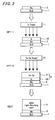
- Fig. 1 shows a basic structure of a thin-film solar cell produced from a general compound semiconductor, which comprises a SLG (soda lime glass) substrate 1 on which a back molybdenum (Mo) electrode layer (positive electrode) 2, a p-type light absorbing layer 5, an n-type heterojunction buffer layer 6 and a transparent electrode layer (negative electrode) 7 are subsequently formed in the described order.
- SLG silica lime glass
- Mo molybdenum
- the light absorbing layer 5 is made in the form of a CIGS (Copper-Indium-Gallium-Selenium) thin film made of Cu (In+Ga) Se2 of I-III-VI2 group based on Cu, (In, Ga), Se, which possesses high power conversion efficiency exceeding 18%.
- CIGS Copper-Indium-Gallium-Selenium
- US Patent No.4611091 discloses a method of forming a heterojunction buffer layer most suited to a light absorbing layer of CIS by chemically growing a thin film of CdS representing a compound semiconductor of II-VI group from a solution.
- Japanese Laying-Open Patent Publication No.H-8--330614 describes a heterojunction buffer layer of Zn which does not contain harmful metal such as cadmium and possesses high power conversion efficiency.
- the above-described conventional compound thin film solar cells involve such a common problem that a defect easily occur in the junction between a p-type semiconductor light absorbing layer and an n-type semiconductor buffer layer because two layers quite differ from each other by their chemical compositions.
- a buffer layer of InS (InS, InO, InOH) is formed by a CBD method that has been developed to attain the uniformity of composition and reproducibility of the product (see reference “ Solar Energy Materials & Solar Cells” 69, 2001, pp.131-137 ).
- an object of the present invention is to provide a method of fabricating a solar cell having an n-type buffer layer providing a heterojunction with a light absorbing layer formed on a back electrode, wherein the buffer layer is formed by CBD (Chemical Bath Deposition) process using a aqueous solution for dipping the light absorbing layer in such a way that particles can be deposited on the light absorbing layer to form a buffer layer of InS, which has a grain structure improved to pass even light of short wavelengths.
- CBD Chemical Bath Deposition
- Another object of the present invention is to provide a method of fabricating a solar cell having an n-type buffer layer formed for providing a heterojunction with a light absorbing layer formed on a back electrode, wherein the buffer layer is formed by CBD of particles of n-type semiconductor material.
- the CBD process according to the present invention provides a buffer layer of n-type semiconductor material, which is featured by gradually or step-by-step increased sizes of deposited particles in the outward direction from the light absorbing layer.
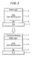
- FIGs. 2 and 3 there is shown a process of fabricating a compound semiconductor thin-film solar cell.
- a molybdenum (Mo) electrode layer 2 serving as a back electrode is first formed by sputtering on a SLG (soda lime glass) substrate 1.
- an indium (In) layer 32 is formed on the back electrode layer 2 by the first sputtering process SPT-1 using a single In target T1 and a copper-gallium (Cu-Ga) alloy layer 31 is formed thereon by the second sputtering process SPT-2 using a Cu-Ga alloy target T2 to form a laminated metal precursor 3 composed of the In layer 32 and the Cu-Ga alloy layer 31.
- the precursor 3 is then treated by heat (by the heat treatment process HEAT) in the atmosphere of selenium (Se) to form a thin film light absorbing layer 5 of CIGS.
- a laminated precursor 3 is fabricated by forming first an In layer 32 and then a Cu-Ga alloy layer 31 on a Mo electrode layer 2, thereby preventing the formation of an alloy of elements diffused in solid phase at a boundary between the precursor 3 and the Mo electrode layer 2.
- This can also facilitate In component to sufficiently diffuse in the precursor on the side of the Mo electrode layer 2 in the process of selenizing the laminated precursor 3 by heating in the selenium atmosphere, simultaneously preventing slowly diffusing elements Ca from segregating at the boundary of the Mo electrode layer 2 and forming thereat a different alloy layer of Cu-Ga-Se which is inferior in its crystal structure.
- the CIGS light absorbing layer 5 thus fabricated can possess high quality P-type semiconductor structure featured by the homogeneous crystal structure of Cu(In+Ga)Se2.
- the light absorbing layer 5 can be featured by high performance and high strength of adhesion between the Mo electrode layer 2 and the light absorbing layer 5 and is free from the formation of a strange layer (Cu-Ga-Se layer) having an inferior crystal structure and possessing conductivity. Consequently, a solar cell fabricated based on the thus fabricated light absorbing layer can possess high strength and is free from leakage from/to other cells when it is used in practice.
- a n-type buffer layer 6 for providing a heterojunction with the p-type layer 5 and a transparent electrode layer 7 of ZnS is further formed by sputtering on the buffer layer 6.
- the buffer layer 6 of InS is formed by wet chemical bath deposition (CBD) using an aqueous solution of indium chloride and thioacetamide.
- CBD wet chemical bath deposition
- the aqueous solution is prepared as a 1:1 mixture of two solutions: 0.01M/l of indium-3-chloride-4-hydrate (InCl 3 • 4H2O) and 0.30M/l of thioacetamide (CH3CSNH2).
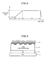
- the buffer layer 6 is formed by CBD using the above-prepared aqueous solution according to the following process shown in Fig. 4 .
- the surface of the light absorbing layer 5 is dipped in the aqueous solution at a temperature T1 (°C) for a preset time t1 (5 ⁇ 10 minutes) while stirring the solution. Stirring of the solution is continued until the buffer layer 6 is completely formed.
- the temperature of the solution is increased to a preset value T2 (about 60°C) for a preset time t2 (about 10 minutes) while the surface of the light absorbing layer is kept as dipped in the solution.
- the dipping of the light absorbing layer in the solution being kept at the preset temperature T2 is continued further for a preset time t3 (about 40 minutes) after the solution reached the temperature T2 at the end of the second step.
- the bluffer layer 6 formed on the light absorbing layer is washed with an overflow of pure water.
- the above-described process provides an In-layer of fine particles deposited by the first step, an In-layer of larger (than those deposited by the first step) particles deposited by the second step and an In-layer of further larger (than those deposited by the second step) particles deposited by the third step.
- the aqueous solution is almost transparent solution which slightly assumes yellow color of thioacetamide at a room temperature.
- the process of forming the buffer layer 6 on the light absorbing layer by depositing particles of In with growth of colloids in the aqueous solution is as follows:
- the solution is emulsified as its temperature rises. With progress of chemical reaction, the emulsion gradually changes its color from deep white to yellow. Since InS is an orange solid in itself, the emulsion represents that InS-crystals are growing in the solution. The change of color of the solution from white to yellow can be considered to indicate that InS particles in the solution are further growing to have larger sizes.
- the white colloid has particles which are smaller in size than the wavelength of yellow light.
- Yellow colloid has In-particles which are grown large enough to assume its orange color by reflecting orange color light.
- the speed of changing color of the solution from white to yellow relates to a ratio of concentration of indium chloride to concentration of thioacetamide in the aqueous solution.
- the color changing speed is apt to increase as the relative concentration of thioacetamide in the solution is lower.
- the buffer layer can grow on the light absorbing layer 5 dipped in the aqueous solution during the time of heating the solution from the room temperature to the specified temperature but the buffer layer does not grow in the emulsion having reached the specified temperature.
- the process of steps 1 to 3 cause particles of InS to deposit from the solution onto the surface of the light absorbing layer by stepwise increasing sizes of deposits.
- This can create a buffer layer 6 having a structure featured by continuous distribution of Ins particles with stepwise increased sizes.
- the buffer layer 6 tightly adheres to a rough surface of the light absorbing layer 5 with an improved coverage.
- the reason why the layer cannot grow in the emulsion is considered by that large particles can have a small contact surface with the light absorbing layer 5. It is also considered that the deposit of small particles serves as adhesive to grow the buffer layer 6.
- InS-layer in a solar cell is disadvantageous since InS has a small bandgap and hard to pass light of short wavelengths.
- the quality of the buffer layer is changed by regulating pH of the aqueous solution in steps 1 to 3.
- the aqueous solution is used at PH of 1 to 3.5 to 12.0 in steps 1 and 2 while the aqueous solution is used at pH of 3.5 to 12.0 in step 3.
- the lower side deposition of the buffer layer 6 is rich in InS by regulating the pH of the aqueous solution to a acidic value of a pH scale while the upper side deposition is rich in InOH • InO by regulating the pH of the solution to a alkaline value.
- the quality of the buffer layer 6 can be changed.
- An In2S3-rich layer obtained by regulating the pH of the solution to a value of the acidic side can effectively cover the top surface of the light absorbing layer 5 achieving the junction best suited to the layer 5.
- the buffer layer 6 To prevent a plasma damage from reaching the junction surface with the buffer layer 6 in the process of forming the transparent electrode 7, it is necessary to increase the thickness of the buffer layer 6. However, it is disadvantageous to increase the thickness of the InS-rich layer because InS has a small bandgap and may deteriorate the optical transmittance of the layer. On the contrary, the layer rich in In(OH)3 • In2O3, which is obtained by regulating the pH of the solution to the alkaline-side value, has a larger bandgap and can be used as a transparent conducting layer.
- a method of fabricating a thin-film compound solar cell having an n-type buffer layer formed therein for providing a hetero-junction with a p-type compound semiconductor light absorbing layer formed on a back electrode wherein the buffer layer is formed by applying a chemical bath deposition (CBD) process using an aqueous solution for dipping the light absorbing layer to deposit particles on the surface thereof.
- CBD chemical bath deposition
- the temperature of the solution is controlled from low to high to increase sizes of the particles to be deposited on the light absorbing layer so as to form the buffer layer which possesses a high optical transmittance, tight adherence to the light absorbing layer and conformity with the transparent electrode formed thereon though it is made of InS material generally possessing a small bandgap and hard to pass light of short wavelengths.
- a method of fabricating a thin-film compound solar cell having an n-type buffer layer formed therein for providing a hetero-junction with a p-type compound semiconductor light absorbing layer formed on a back electrode wherein the buffer layer is formed by applying a chemical bath deposition (CBD) process using an aqueous solution for dipping the light absorbing layer to deposit particles on the surface thereof.
- CBD chemical bath deposition
- the process provides a buffer layer of n-type semiconductor material, which is featured by gradually or step-by-step increased sizes of deposited particles in the outward direction from the light absorbing layer.
- the buffer layer thus formed possesses a high optical transmittance, tight adherence to the light absorbing layer and conformity with the transparent electrode formed thereon though it is made of InS material generally possessing a small bandgap and hard to pass light of short wavelengths.
Description
- The present invention relates to a compound semiconductor thin-film solar cell having an n-type buffer layer for heterojunction with a light absorbing layer and a method of fabricating the same compound semiconductor thin-film solar cell.
-
Fig. 1 shows a basic structure of a thin-film solar cell produced from a general compound semiconductor, which comprises a SLG (soda lime glass)substrate 1 on which a back molybdenum (Mo) electrode layer (positive electrode) 2, a p-typelight absorbing layer 5, an n-typeheterojunction buffer layer 6 and a transparent electrode layer (negative electrode) 7 are subsequently formed in the described order. - In the thin-film compound semiconductor solar cell, the
light absorbing layer 5 is made in the form of a CIGS (Copper-Indium-Gallium-Selenium) thin film made of Cu (In+Ga) Se2 of I-III-VI2 group based on Cu, (In, Ga), Se, which possesses high power conversion efficiency exceeding 18%. -
US Patent No.4611091 discloses a method of forming a heterojunction buffer layer most suited to a light absorbing layer of CIS by chemically growing a thin film of CdS representing a compound semiconductor of II-VI group from a solution. - Japanese Laying-Open Patent Publication No.H-8--330614 describes a heterojunction buffer layer of Zn which does not contain harmful metal such as cadmium and possesses high power conversion efficiency.
- The above-described conventional compound thin film solar cells involve such a common problem that a defect easily occur in the junction between a p-type semiconductor light absorbing layer and an n-type semiconductor buffer layer because two layers quite differ from each other by their chemical compositions.
- While the light absorbing layer is dipped in the solution, two process of diffusing Zn element into the light absorbing layer and forming a ZnS film concurrently take place, which may easily cause variations in power conversion efficiency of the product from the crystallinity and surface conditions of the light absorbing layer.
- To obtain a heterojunction suitable to the light absorbing layer of CIGS thin film, a buffer layer of InS (InS, InO, InOH) is formed by a CBD method that has been developed to attain the uniformity of composition and reproducibility of the product (see reference "Solar Energy Materials & Solar Cells" 69, 2001, pp.131-137).
- However, the formation of a buffer layer of InS group by the Chemical Bath Deposition (CBD) method for forming a heterojunction suited to the light absorbing layer of CIGS thin film still involves a problem that the buffer layer of InS has a small band gap and generally be hard to pass light of short wavelengths. Namely, it cannot result in high Jsc.
- Accordingly, an object of the present invention is to provide a method of fabricating a solar cell having an n-type buffer layer providing a heterojunction with a light absorbing layer formed on a back electrode, wherein the buffer layer is formed by CBD (Chemical Bath Deposition) process using a aqueous solution for dipping the light absorbing layer in such a way that particles can be deposited on the light absorbing layer to form a buffer layer of InS, which has a grain structure improved to pass even light of short wavelengths. The CBD process according to the present invention is defined in
claim 2. - Another object of the present invention is to provide a method of fabricating a solar cell having an n-type buffer layer formed for providing a heterojunction with a light absorbing layer formed on a back electrode, wherein the buffer layer is formed by CBD of particles of n-type semiconductor material. The CBD process according to the present invention provides a buffer layer of n-type semiconductor material, which is featured by gradually or step-by-step increased sizes of deposited particles in the outward direction from the light absorbing layer.
-
-
Fig. 1 is a sectional illustration of a basic structure of a solar cell of general compound semiconductors. -
Fig. 2 illustrates a process of forming a back electrode and a light absorbing layer on a substrate of soda lime glass (SLG). -
Fig. 3 illustrates a process of forming a buffer layer and a transparent electrode layer on a light absorbing layer. -
Fig. 4 is a graph showing temperature characteristic of aqueous solution when forming a buffer layer by the CBD method according to an embodiment of the present invention. -
Fig. 5 is a sectional illustration of forming by CBD a buffer layer of InS particles on a light absorbing layer. - In
Figs. 2 and3 , there is shown a process of fabricating a compound semiconductor thin-film solar cell. - As shown in
Fig. 2 , a molybdenum (Mo)electrode layer 2 serving as a back electrode is first formed by sputtering on a SLG (soda lime glass)substrate 1. Next, an indium (In)layer 32 is formed on theback electrode layer 2 by the first sputtering process SPT-1 using a single In target T1 and a copper-gallium (Cu-Ga)alloy layer 31 is formed thereon by the second sputtering process SPT-2 using a Cu-Ga alloy target T2 to form a laminatedmetal precursor 3 composed of theIn layer 32 and the Cu-Ga alloy layer 31. Theprecursor 3 is then treated by heat (by the heat treatment process HEAT) in the atmosphere of selenium (Se) to form a thin filmlight absorbing layer 5 of CIGS. - As described above, a laminated
precursor 3 is fabricated by forming first anIn layer 32 and then a Cu-Ga alloy layer 31 on aMo electrode layer 2, thereby preventing the formation of an alloy of elements diffused in solid phase at a boundary between theprecursor 3 and theMo electrode layer 2. This can also facilitate In component to sufficiently diffuse in the precursor on the side of theMo electrode layer 2 in the process of selenizing the laminatedprecursor 3 by heating in the selenium atmosphere, simultaneously preventing slowly diffusing elements Ca from segregating at the boundary of theMo electrode layer 2 and forming thereat a different alloy layer of Cu-Ga-Se which is inferior in its crystal structure. The CIGSlight absorbing layer 5 thus fabricated can possess high quality P-type semiconductor structure featured by the homogeneous crystal structure of Cu(In+Ga)Se2. The light absorbinglayer 5 can be featured by high performance and high strength of adhesion between theMo electrode layer 2 and thelight absorbing layer 5 and is free from the formation of a strange layer (Cu-Ga-Se layer) having an inferior crystal structure and possessing conductivity. Consequently, a solar cell fabricated based on the thus fabricated light absorbing layer can possess high strength and is free from leakage from/to other cells when it is used in practice. - On the p-type
light absorbing layer 5, as shown inFig. 3 , there is then formed a n-type buffer layer 6 for providing a heterojunction with the p-type layer 5 and atransparent electrode layer 7 of ZnS is further formed by sputtering on thebuffer layer 6. - According to the present invention, the
buffer layer 6 of InS is formed by wet chemical bath deposition (CBD) using an aqueous solution of indium chloride and thioacetamide. In practice, the aqueous solution is prepared as a 1:1 mixture of two solutions: 0.01M/l of indium-3-chloride-4-hydrate (InCl 3 • 4H2O) and 0.30M/l of thioacetamide (CH3CSNH2). - The
buffer layer 6 is formed by CBD using the above-prepared aqueous solution according to the following process shown inFig. 4 . - In the first step, the surface of the
light absorbing layer 5 is dipped in the aqueous solution at a temperature T1 (°C) for a preset time t1 (5∼10 minutes) while stirring the solution. Stirring of the solution is continued until thebuffer layer 6 is completely formed. - In the second step, the temperature of the solution is increased to a preset value T2 (about 60°C) for a preset time t2 (about 10 minutes) while the surface of the light absorbing layer is kept as dipped in the solution.
- In the third step, the dipping of the light absorbing layer in the solution being kept at the preset temperature T2 is continued further for a preset time t3 (about 40 minutes) after the solution reached the temperature T2 at the end of the second step. The
bluffer layer 6 formed on the light absorbing layer is washed with an overflow of pure water. - The above-described process provides an In-layer of fine particles deposited by the first step, an In-layer of larger (than those deposited by the first step) particles deposited by the second step and an In-layer of further larger (than those deposited by the second step) particles deposited by the third step.
- This is explained as follows:
- The aqueous solution is almost transparent solution which slightly assumes yellow color of thioacetamide at a room temperature.
- The process of forming the
buffer layer 6 on the light absorbing layer by depositing particles of In with growth of colloids in the aqueous solution is as follows: - The solution is emulsified as its temperature rises. With progress of chemical reaction, the emulsion gradually changes its color from deep white to yellow. Since InS is an orange solid in itself, the emulsion represents that InS-crystals are growing in the solution. The change of color of the solution from white to yellow can be considered to indicate that InS particles in the solution are further growing to have larger sizes.
- In other words, the white colloid has particles which are smaller in size than the wavelength of yellow light. Yellow colloid has In-particles which are grown large enough to assume its orange color by reflecting orange color light.
- The speed of changing color of the solution from white to yellow relates to a ratio of concentration of indium chloride to concentration of thioacetamide in the aqueous solution. The color changing speed is apt to increase as the relative concentration of thioacetamide in the solution is lower.
- It has been found that the buffer layer can grow on the
light absorbing layer 5 dipped in the aqueous solution during the time of heating the solution from the room temperature to the specified temperature but the buffer layer does not grow in the emulsion having reached the specified temperature. - Accordingly, the process of
steps 1 to 3 cause particles of InS to deposit from the solution onto the surface of the light absorbing layer by stepwise increasing sizes of deposits. This can create abuffer layer 6 having a structure featured by continuous distribution of Ins particles with stepwise increased sizes. As the result of this, as shown inFig. 5 , thebuffer layer 6 tightly adheres to a rough surface of thelight absorbing layer 5 with an improved coverage. - The reason why the layer cannot grow in the emulsion is considered by that large particles can have a small contact surface with the
light absorbing layer 5. It is also considered that the deposit of small particles serves as adhesive to grow thebuffer layer 6. - The use of a layer of In-particles as the
buffer layer 6 offers the following advantage: - a) Expanding a bandgap by the effect of particle sizes;
- b) Expanding a bandgap by the effect of particle surfacea;
- c) Improvement of durability against a plasma damage; and
- d) Reduction of shunt path by the high resistance of the layer.
- It has been considered that the use of the InS-layer in a solar cell is disadvantageous since InS has a small bandgap and hard to pass light of short wavelengths.
- The above-mentioned disadvantage can be overcome by making the layer composed of fine particles of InS. According to the present invention, the quality of the buffer layer is changed by regulating pH of the aqueous solution in
steps 1 to 3. In practice, the aqueous solution is used at PH of 1 to 3.5 to 12.0 insteps step 3. Thus, the lower side deposition of thebuffer layer 6 is rich in InS by regulating the pH of the aqueous solution to a acidic value of a pH scale while the upper side deposition is rich in InOH • InO by regulating the pH of the solution to a alkaline value. - When pH of the solution of indium chloride and thioacetamide is regulated to about 1-3.5, then the following chemical reaction takes place:
2InCl3+3CH3CSNH2+6H2O → In2S3+3CH3CO2+3NH4+6HCl
- When pH of the aqueous solution containing trivalent ions is regulated to 3.4-12, then the following chemical reaction takes place:
InCl3+3H2O ←→In (OH) 3+3HCl
- By regulating the pH value of the aqueous solution using the above-described chemical reactions, the quality of the
buffer layer 6 can be changed. - Consequently, it becomes possible to achieve the following optimum interfacial condition between the light absorbing
layer 5 and thebuffer layer 6 as well as thebuffer layer 6 and thetransparent electrode 7. - An In2S3-rich layer obtained by regulating the pH of the solution to a value of the acidic side can effectively cover the top surface of the
light absorbing layer 5 achieving the junction best suited to thelayer 5. - To prevent a plasma damage from reaching the junction surface with the
buffer layer 6 in the process of forming thetransparent electrode 7, it is necessary to increase the thickness of thebuffer layer 6. However, it is disadvantageous to increase the thickness of the InS-rich layer because InS has a small bandgap and may deteriorate the optical transmittance of the layer. On the contrary, the layer rich in In(OH)3 • In2O3, which is obtained by regulating the pH of the solution to the alkaline-side value, has a larger bandgap and can be used as a transparent conducting layer. Therefore, it is desirable to form a thicker layer rich in In (OH)3 • In2O3, which can be free from the affection of plasma damage in the process of forming atransparent electrode 7 and can attain the suitable conformity to thetransparent electrode 7 without decreasing the optical transmittance of the buffer layer. - As is apparent from the foregoing, according to the present invention, it is possible to provide a method of fabricating a thin-film compound solar cell having an n-type buffer layer formed therein for providing a hetero-junction with a p-type compound semiconductor light absorbing layer formed on a back electrode, wherein the buffer layer is formed by applying a chemical bath deposition (CBD) process using an aqueous solution for dipping the light absorbing layer to deposit particles on the surface thereof. In this process, the temperature of the solution is controlled from low to high to increase sizes of the particles to be deposited on the light absorbing layer so as to form the buffer layer which possesses a high optical transmittance, tight adherence to the light absorbing layer and conformity with the transparent electrode formed thereon though it is made of InS material generally possessing a small bandgap and hard to pass light of short wavelengths.
- According to the present invention, it is also possible to provide a method of fabricating a thin-film compound solar cell having an n-type buffer layer formed therein for providing a hetero-junction with a p-type compound semiconductor light absorbing layer formed on a back electrode, wherein the buffer layer is formed by applying a chemical bath deposition (CBD) process using an aqueous solution for dipping the light absorbing layer to deposit particles on the surface thereof. The process provides a buffer layer of n-type semiconductor material, which is featured by gradually or step-by-step increased sizes of deposited particles in the outward direction from the light absorbing layer. The buffer layer thus formed possesses a high optical transmittance, tight adherence to the light absorbing layer and conformity with the transparent electrode formed thereon though it is made of InS material generally possessing a small bandgap and hard to pass light of short wavelengths.
Claims (2)
- A thin-film compound solar cell having an n-type buffer layer of InS formed by chemical bath deposition (CBD) for providing heterojunction with a p-type semiconductor light absorbing layer comprising I-III-VI-group material formed on a back electrode, wherein the buffer layer is formed of layered deposits of particles of n-type semiconductor material of InS and wherein the lower side deposition of the buffer layer is rich in InS and the upper side deposition is rich in InOH·InO.
- A method of fabricating a thin-film compound solar cell having an n-type buffer layer of InS formed for providing heterojunction with a p-type semiconductor light absorbing layer comprising I-III-VI-group-material formed on a back electrode, wherein the buffer layer is formed on the light absorbing layer by chemical bath deposition (CBD) process using an aqueous solution comprising indium chloride and thioacetamide for dipping therein a surface of the light absorbing layer, wherein, in the CBD process of forming the buffer layer on the light absorbing layer whose surface is dipped in an aqueous solution for depositing particles thereon, pH of the solution is changed from an acidic value to an alkaline value to cause the buffer layer to have different quality of deposit layers therein.
Applications Claiming Priority (2)
| Application Number | Priority Date | Filing Date | Title |
|---|---|---|---|
| JP2002129381A JP4055053B2 (en) | 2002-03-26 | 2002-03-26 | Compound thin film solar cell and manufacturing method thereof |
| EP03712838A EP1489666B1 (en) | 2002-03-26 | 2003-03-24 | Process for producing a compound thin-film solar cell |
Related Parent Applications (1)
| Application Number | Title | Priority Date | Filing Date |
|---|---|---|---|
| EP03712838.6 Division | 2003-03-24 |
Publications (3)
| Publication Number | Publication Date |
|---|---|
| EP2216824A2 EP2216824A2 (en) | 2010-08-11 |
| EP2216824A3 EP2216824A3 (en) | 2010-09-22 |
| EP2216824B1 true EP2216824B1 (en) | 2012-07-18 |
Family
ID=28450001
Family Applications (2)
| Application Number | Title | Priority Date | Filing Date |
|---|---|---|---|
| EP03712838A Expired - Fee Related EP1489666B1 (en) | 2002-03-26 | 2003-03-24 | Process for producing a compound thin-film solar cell |
| EP10161750A Expired - Fee Related EP2216824B1 (en) | 2002-03-26 | 2003-03-24 | Compound thin-film solar cell and process for producing the same |
Family Applications Before (1)
| Application Number | Title | Priority Date | Filing Date |
|---|---|---|---|
| EP03712838A Expired - Fee Related EP1489666B1 (en) | 2002-03-26 | 2003-03-24 | Process for producing a compound thin-film solar cell |
Country Status (5)
| Country | Link |
|---|---|
| US (3) | US7939745B2 (en) |
| EP (2) | EP1489666B1 (en) |
| JP (1) | JP4055053B2 (en) |
| AU (1) | AU2003220984A1 (en) |
| WO (1) | WO2003081684A1 (en) |
Families Citing this family (57)
| Publication number | Priority date | Publication date | Assignee | Title |
|---|---|---|---|---|
| EE00584U1 (en) * | 2004-06-07 | 2006-01-16 | Tallinna Tehnikaülikool | A method of fabricating a CuInS2 absorber solar cell |
| JP4549193B2 (en) * | 2005-01-14 | 2010-09-22 | 本田技研工業株式会社 | Chalcopyrite thin film solar cell and manufacturing method thereof |
| JP2007201304A (en) * | 2006-01-30 | 2007-08-09 | Honda Motor Co Ltd | Solar cell and its manufacturing method |
| US8389852B2 (en) * | 2006-02-22 | 2013-03-05 | Guardian Industries Corp. | Electrode structure for use in electronic device and method of making same |
| US20070215195A1 (en) * | 2006-03-18 | 2007-09-20 | Benyamin Buller | Elongated photovoltaic cells in tubular casings |
| EP2016625B1 (en) * | 2006-04-18 | 2009-09-02 | Dow Corning Corporation | Copper indium diselenide-based photovoltaic device and method of preparing the same |
| WO2007123898A1 (en) * | 2006-04-18 | 2007-11-01 | Dow Corning Corporation | Copper indium diselenide-based photovoltaic device and method of preparing the same |
| US8207442B2 (en) | 2006-04-18 | 2012-06-26 | Itn Energy Systems, Inc. | Reinforcing structures for thin-film photovoltaic device substrates, and associated methods |
| CN101421100B (en) * | 2006-04-18 | 2013-03-27 | 陶氏康宁公司 | Metal foil substrates coated with condensation cured silicon resin compositions |
| US9105776B2 (en) * | 2006-05-15 | 2015-08-11 | Stion Corporation | Method and structure for thin film photovoltaic materials using semiconductor materials |
| JP4925724B2 (en) * | 2006-05-25 | 2012-05-09 | 本田技研工業株式会社 | Solar cell and method for manufacturing the same |
| JP2007317879A (en) * | 2006-05-25 | 2007-12-06 | Honda Motor Co Ltd | Chalcopyrite solar cell, and manufacturing method thereof |
| WO2008036769A2 (en) | 2006-09-19 | 2008-03-27 | Itn Energy Systems, Inc. | Semi-transparent dual layer back contact for bifacial and tandem junction thin-film photovolataic devices |
| US8414961B1 (en) * | 2006-12-13 | 2013-04-09 | Nanosolar, Inc. | Solution deposited transparent conductors |
| US7825329B2 (en) * | 2007-01-03 | 2010-11-02 | Solopower, Inc. | Thin film solar cell manufacturing and integration |
| US20080216885A1 (en) | 2007-03-06 | 2008-09-11 | Sergey Frolov | Spectrally adaptive multijunction photovoltaic thin film device and method of producing same |
| US7977139B2 (en) * | 2007-03-28 | 2011-07-12 | Showa Shell Sekiyu K.K. | Method for manufacturing CIS based thin film solar cell device |
| FR2922364B1 (en) * | 2007-10-12 | 2014-08-22 | Saint Gobain | PROCESS FOR PRODUCING A MOLYBDENE OXIDE ELECTRODE |
| US20090211622A1 (en) * | 2008-02-21 | 2009-08-27 | Sunlight Photonics Inc. | Multi-layered electro-optic devices |
| US20090215215A1 (en) * | 2008-02-21 | 2009-08-27 | Sunlight Photonics Inc. | Method and apparatus for manufacturing multi-layered electro-optic devices |
| US8530262B2 (en) * | 2008-02-28 | 2013-09-10 | Nanosolar, Inc. | Roll-to-roll non-vacuum deposition of transparent conductive electrodes |
| US7842534B2 (en) * | 2008-04-02 | 2010-11-30 | Sunlight Photonics Inc. | Method for forming a compound semi-conductor thin-film |
| US10211353B2 (en) * | 2008-04-14 | 2019-02-19 | Sunlight Photonics Inc. | Aligned bifacial solar modules |
| CN102017203B (en) * | 2008-05-02 | 2013-04-10 | Lg伊诺特有限公司 | Light-emitting element and a production method therefor |
| US8110428B2 (en) * | 2008-11-25 | 2012-02-07 | Sunlight Photonics Inc. | Thin-film photovoltaic devices |
| US8835748B2 (en) | 2009-01-06 | 2014-09-16 | Sunlight Photonics Inc. | Multi-junction PV module |
| US10297707B1 (en) * | 2009-02-23 | 2019-05-21 | Tatiana Globus | Thin film photovoltaic cell system and method of manufacture |
| JP2012530378A (en) * | 2009-06-16 | 2012-11-29 | エルジー イノテック カンパニー リミテッド | Solar cell and manufacturing method thereof |
| KR101081194B1 (en) * | 2009-06-16 | 2011-11-07 | 엘지이노텍 주식회사 | Fabricating device of solar cell and method of fabricating using the same |
| KR101028192B1 (en) | 2009-06-16 | 2011-04-11 | 엘지이노텍 주식회사 | Solar cell and method of fabricating the same |
| JP2011018857A (en) * | 2009-07-10 | 2011-01-27 | Mitsubishi Heavy Ind Ltd | Method of manufacturing photoelectric conversion device |
| US20110017289A1 (en) * | 2009-07-24 | 2011-01-27 | Electronics And Telecommunications Research Institute | Cigs solar cell and method of fabricating the same |
| US8012788B1 (en) | 2009-10-21 | 2011-09-06 | Sunlight Photonics Inc. | Multi-stage formation of thin-films for photovoltaic devices |
| US7910396B2 (en) | 2009-10-21 | 2011-03-22 | Sunlight Photonics, Inc. | Three-stage formation of thin-films for photovoltaic devices |
| KR101091215B1 (en) * | 2009-10-30 | 2011-12-07 | 엘지이노텍 주식회사 | Solar cell and method of fabricating the same |
| CN101840960A (en) * | 2010-02-11 | 2010-09-22 | 昆山正富机械工业有限公司 | Multi-stage cadmium sulfide thin film deposition method |
| CN101820028A (en) * | 2010-02-11 | 2010-09-01 | 昆山正富机械工业有限公司 | Deposition method of multi-section camium sulfide thin film |
| CN102782853A (en) * | 2010-03-05 | 2012-11-14 | 第一太阳能有限公司 | Photovoltaic device with graded buffer layer |
| JP2012054261A (en) * | 2010-08-31 | 2012-03-15 | Kyocera Corp | Photoelectric conversion device, method of manufacturing the same, and photoelectric conversion module |
| JP2012109558A (en) * | 2010-10-29 | 2012-06-07 | Kyocera Corp | Photoelectric conversion element, photoelectric conversion device, and method of manufacturing photoelectric conversion element |
| JP5488436B2 (en) * | 2010-12-07 | 2014-05-14 | 株式会社豊田中央研究所 | Photoelectric element |
| JP5500059B2 (en) * | 2010-12-07 | 2014-05-21 | 株式会社豊田中央研究所 | Photoelectric element |
| JP5701673B2 (en) * | 2011-05-06 | 2015-04-15 | 株式会社東芝 | Photoelectric conversion element and solar cell |
| JP5886622B2 (en) * | 2011-05-30 | 2016-03-16 | 京セラ株式会社 | Method and apparatus for manufacturing compound semiconductor film |
| JP5784125B2 (en) * | 2011-08-30 | 2015-09-24 | 京セラ株式会社 | Method for manufacturing photoelectric conversion element |
| JP5792008B2 (en) * | 2011-09-14 | 2015-10-07 | 本田技研工業株式会社 | Method for manufacturing chalcopyrite solar cell |
| KR101326885B1 (en) | 2011-10-17 | 2013-11-11 | 엘지이노텍 주식회사 | Solar cell and method of fabricating the same |
| KR101306529B1 (en) * | 2011-11-21 | 2013-09-09 | 엘지이노텍 주식회사 | Solar cell and method of fabricating the same |
| JP5258951B2 (en) * | 2011-12-02 | 2013-08-07 | 昭和シェル石油株式会社 | Thin film solar cell |
| US8586457B1 (en) * | 2012-05-17 | 2013-11-19 | Intermolecular, Inc. | Method of fabricating high efficiency CIGS solar cells |
| KR101388419B1 (en) * | 2012-06-14 | 2014-05-12 | 에스엔유 프리시젼 주식회사 | Apparatus for chemical bath deposion and method using the same |
| EP2865012B1 (en) * | 2012-06-20 | 2023-01-18 | Cnbm Research Institute For Advanced Glass Materials Group Co., Ltd. | Coating system for thin film solar cells |
| US8871560B2 (en) * | 2012-08-09 | 2014-10-28 | International Business Machines Corporation | Plasma annealing of thin film solar cells |
| RU2533888C1 (en) * | 2013-07-15 | 2014-11-27 | Федеральное государственное автономное образовательное учреждение высшего профессионального образования "Уральский федеральный университет имени первого Президента России Б.Н. Ельцина" | Solution for hydrochemical sedimentation of semi-conductor films of indium sulphide |
| JP6306388B2 (en) * | 2014-03-24 | 2018-04-04 | 京セラ株式会社 | Method for manufacturing photoelectric conversion device |
| US10727366B2 (en) * | 2016-01-13 | 2020-07-28 | Mecaroenergy Co., Ltd. | Solar cell comprising CIGS light absorbing layer and method for manufacturing same |
| CN110379874B (en) * | 2019-07-25 | 2022-02-11 | 中国科学技术大学 | Solar thin film battery and preparation method thereof |
Family Cites Families (8)
| Publication number | Priority date | Publication date | Assignee | Title |
|---|---|---|---|---|
| US4335266A (en) * | 1980-12-31 | 1982-06-15 | The Boeing Company | Methods for forming thin-film heterojunction solar cells from I-III-VI.sub.2 |
| US4611091A (en) | 1984-12-06 | 1986-09-09 | Atlantic Richfield Company | CuInSe2 thin film solar cell with thin CdS and transparent window layer |
| JPH07240385A (en) * | 1994-02-28 | 1995-09-12 | Ebara Corp | Forming method of sulfur cadmium film and its equipment |
| DE4440878C2 (en) * | 1994-11-16 | 1999-04-29 | Zsw | Compound semiconductor thin-film solar cell and process for its production |
| JP3249342B2 (en) | 1995-05-29 | 2002-01-21 | 昭和シェル石油株式会社 | Heterojunction thin-film solar cell and method of manufacturing the same |
| US5674555A (en) * | 1995-11-30 | 1997-10-07 | University Of Delaware | Process for preparing group Ib-IIIa-VIa semiconducting films |
| US6023020A (en) * | 1996-10-15 | 2000-02-08 | Matsushita Electric Industrial Co., Ltd. | Solar cell and method for manufacturing the same |
| JP3589380B2 (en) * | 1997-06-05 | 2004-11-17 | 松下電器産業株式会社 | Method of manufacturing semiconductor thin film and method of manufacturing thin film solar cell |
-
2002
- 2002-03-26 JP JP2002129381A patent/JP4055053B2/en not_active Expired - Fee Related
-
2003
- 2003-03-24 AU AU2003220984A patent/AU2003220984A1/en not_active Abandoned
- 2003-03-24 US US10/509,303 patent/US7939745B2/en active Active
- 2003-03-24 WO PCT/JP2003/003500 patent/WO2003081684A1/en active Application Filing
- 2003-03-24 EP EP03712838A patent/EP1489666B1/en not_active Expired - Fee Related
- 2003-03-24 EP EP10161750A patent/EP2216824B1/en not_active Expired - Fee Related
-
2011
- 2011-05-09 US US13/103,659 patent/US20110203646A1/en not_active Abandoned
-
2014
- 2014-02-27 US US14/192,701 patent/US20140224309A1/en not_active Abandoned
Also Published As
| Publication number | Publication date |
|---|---|
| EP2216824A3 (en) | 2010-09-22 |
| WO2003081684A1 (en) | 2003-10-02 |
| JP4055053B2 (en) | 2008-03-05 |
| EP2216824A2 (en) | 2010-08-11 |
| US7939745B2 (en) | 2011-05-10 |
| US20140224309A1 (en) | 2014-08-14 |
| EP1489666A4 (en) | 2008-06-04 |
| AU2003220984A1 (en) | 2003-10-08 |
| US20050236032A1 (en) | 2005-10-27 |
| EP1489666A1 (en) | 2004-12-22 |
| US20110203646A1 (en) | 2011-08-25 |
| EP1489666B1 (en) | 2011-10-05 |
| JP2003282909A (en) | 2003-10-03 |
Similar Documents
| Publication | Publication Date | Title |
|---|---|---|
| EP2216824B1 (en) | Compound thin-film solar cell and process for producing the same | |
| US7141449B2 (en) | Method of fabricating a compound semiconductor thin-layer solar cell | |
| US5078804A (en) | I-III-VI2 based solar cell utilizing the structure CuInGaSe2 CdZnS/ZnO | |
| US8026122B1 (en) | Metal species surface treatment of thin film photovoltaic cell and manufacturing method | |
| US5141564A (en) | Mixed ternary heterojunction solar cell | |
| US5112410A (en) | Cadmium zinc sulfide by solution growth | |
| US8691619B2 (en) | Laminated structure for CIS based solar cell, and integrated structure and manufacturing method for CIS based thin-film solar cell | |
| US7018858B2 (en) | Light absorbing layer producing method | |
| US20060219288A1 (en) | Process and photovoltaic device using an akali-containing layer | |
| US9166077B2 (en) | Thin film solar cell | |
| US8258001B2 (en) | Method and apparatus for forming copper indium gallium chalcogenide layers | |
| KR20070055497A (en) | Cis type compound semiconductor thin film solar cell and method for preparing light-absorbing layer of said solar cell | |
| JP4549570B2 (en) | Method for manufacturing heterojunction thin film solar cell | |
| WO2011158899A1 (en) | Cis-based thin film solar cell | |
| JP4320529B2 (en) | Compound thin film solar cell and manufacturing method thereof | |
| KR20130052478A (en) | Solar cell and method of fabricating the same | |
| Su et al. | Cation substitution of CZTS solar cell with> 10% efficiency | |
| US20160005916A1 (en) | Method of Making Photovoltaic Devices | |
| WO2015120512A1 (en) | A photovoltaic cell and a method of forming a photovoltaic cell | |
| Shafarman et al. | Advances in CuInSe2 and CdTe thin film solar cells | |
| KR102596328B1 (en) | Preparation method for CZTS thin film solar cell absorbing layer, CZTS thin film solar cell absorbing layer prepared therefrom | |
| KR102513863B1 (en) | Flexible CZTSSe thin film solar cells and manufacturing method thereof | |
| Dale et al. | Applications of Electrochemistry in the Fabrication and Characterization of Thin‐Film Solar Cells | |
| KR101283106B1 (en) | Solar cell and method for fabricating unsing the same | |
| US20220246786A1 (en) | Method for producing a double graded cdsete thin film structure |
Legal Events
| Date | Code | Title | Description |
|---|---|---|---|
| PUAI | Public reference made under article 153(3) epc to a published international application that has entered the european phase |
Free format text: ORIGINAL CODE: 0009012 |
|
| 17P | Request for examination filed |
Effective date: 20100503 |
|
| AC | Divisional application: reference to earlier application |
Ref document number: 1489666 Country of ref document: EP Kind code of ref document: P |
|
| AK | Designated contracting states |
Kind code of ref document: A2 Designated state(s): DE SE |
|
| RIN1 | Information on inventor provided before grant (corrected) |
Inventor name: AOKI, SATOSHI |
|
| PUAL | Search report despatched |
Free format text: ORIGINAL CODE: 0009013 |
|
| AK | Designated contracting states |
Kind code of ref document: A3 Designated state(s): DE SE |
|
| 17Q | First examination report despatched |
Effective date: 20100930 |
|
| RIN1 | Information on inventor provided before grant (corrected) |
Inventor name: AOKI, SATOSHI |
|
| GRAP | Despatch of communication of intention to grant a patent |
Free format text: ORIGINAL CODE: EPIDOSNIGR1 |
|
| GRAS | Grant fee paid |
Free format text: ORIGINAL CODE: EPIDOSNIGR3 |
|
| GRAA | (expected) grant |
Free format text: ORIGINAL CODE: 0009210 |
|
| AC | Divisional application: reference to earlier application |
Ref document number: 1489666 Country of ref document: EP Kind code of ref document: P |
|
| AK | Designated contracting states |
Kind code of ref document: B1 Designated state(s): DE SE |
|
| REG | Reference to a national code |
Ref country code: DE Ref legal event code: R096 Ref document number: 60341588 Country of ref document: DE Effective date: 20120906 |
|
| PG25 | Lapsed in a contracting state [announced via postgrant information from national office to epo] |
Ref country code: SE Free format text: LAPSE BECAUSE OF FAILURE TO SUBMIT A TRANSLATION OF THE DESCRIPTION OR TO PAY THE FEE WITHIN THE PRESCRIBED TIME-LIMIT Effective date: 20120718 |
|
| PLBE | No opposition filed within time limit |
Free format text: ORIGINAL CODE: 0009261 |
|
| STAA | Information on the status of an ep patent application or granted ep patent |
Free format text: STATUS: NO OPPOSITION FILED WITHIN TIME LIMIT |
|
| 26N | No opposition filed |
Effective date: 20130419 |
|
| REG | Reference to a national code |
Ref country code: DE Ref legal event code: R097 Ref document number: 60341588 Country of ref document: DE Effective date: 20130419 |
|
| REG | Reference to a national code |
Ref country code: DE Ref legal event code: R084 Ref document number: 60341588 Country of ref document: DE |
|
| REG | Reference to a national code |
Ref country code: DE Ref legal event code: R084 Ref document number: 60341588 Country of ref document: DE Effective date: 20141120 |
|
| PGFP | Annual fee paid to national office [announced via postgrant information from national office to epo] |
Ref country code: DE Payment date: 20190312 Year of fee payment: 17 |
|
| REG | Reference to a national code |
Ref country code: DE Ref legal event code: R119 Ref document number: 60341588 Country of ref document: DE |
|
| PG25 | Lapsed in a contracting state [announced via postgrant information from national office to epo] |
Ref country code: DE Free format text: LAPSE BECAUSE OF NON-PAYMENT OF DUE FEES Effective date: 20201001 |