EP2216104B1 - Ultrasonic probe, ultrasonic imaging apparatus and fabricating method thereof - Google Patents
Ultrasonic probe, ultrasonic imaging apparatus and fabricating method thereof Download PDFInfo
- Publication number
- EP2216104B1 EP2216104B1 EP10151791.0A EP10151791A EP2216104B1 EP 2216104 B1 EP2216104 B1 EP 2216104B1 EP 10151791 A EP10151791 A EP 10151791A EP 2216104 B1 EP2216104 B1 EP 2216104B1
- Authority
- EP
- European Patent Office
- Prior art keywords
- pad
- ultrasonic probe
- holes
- printed circuit
- circuit board
- Prior art date
- Legal status (The legal status is an assumption and is not a legal conclusion. Google has not performed a legal analysis and makes no representation as to the accuracy of the status listed.)
- Active
Links
Images





Classifications
-
- G—PHYSICS
- G01—MEASURING; TESTING
- G01N—INVESTIGATING OR ANALYSING MATERIALS BY DETERMINING THEIR CHEMICAL OR PHYSICAL PROPERTIES
- G01N29/00—Investigating or analysing materials by the use of ultrasonic, sonic or infrasonic waves; Visualisation of the interior of objects by transmitting ultrasonic or sonic waves through the object
- G01N29/22—Details, e.g. general constructional or apparatus details
- G01N29/24—Probes
-
- A—HUMAN NECESSITIES
- A61—MEDICAL OR VETERINARY SCIENCE; HYGIENE
- A61B—DIAGNOSIS; SURGERY; IDENTIFICATION
- A61B8/00—Diagnosis using ultrasonic, sonic or infrasonic waves
-
- A—HUMAN NECESSITIES
- A61—MEDICAL OR VETERINARY SCIENCE; HYGIENE
- A61B—DIAGNOSIS; SURGERY; IDENTIFICATION
- A61B8/00—Diagnosis using ultrasonic, sonic or infrasonic waves
- A61B8/44—Constructional features of the ultrasonic, sonic or infrasonic diagnostic device
- A61B8/4444—Constructional features of the ultrasonic, sonic or infrasonic diagnostic device related to the probe
- A61B8/4455—Features of the external shape of the probe, e.g. ergonomic aspects
-
- A—HUMAN NECESSITIES
- A61—MEDICAL OR VETERINARY SCIENCE; HYGIENE
- A61B—DIAGNOSIS; SURGERY; IDENTIFICATION
- A61B8/00—Diagnosis using ultrasonic, sonic or infrasonic waves
- A61B8/44—Constructional features of the ultrasonic, sonic or infrasonic diagnostic device
- A61B8/4483—Constructional features of the ultrasonic, sonic or infrasonic diagnostic device characterised by features of the ultrasound transducer
-
- B—PERFORMING OPERATIONS; TRANSPORTING
- B06—GENERATING OR TRANSMITTING MECHANICAL VIBRATIONS IN GENERAL
- B06B—METHODS OR APPARATUS FOR GENERATING OR TRANSMITTING MECHANICAL VIBRATIONS OF INFRASONIC, SONIC, OR ULTRASONIC FREQUENCY, e.g. FOR PERFORMING MECHANICAL WORK IN GENERAL
- B06B1/00—Methods or apparatus for generating mechanical vibrations of infrasonic, sonic, or ultrasonic frequency
- B06B1/02—Methods or apparatus for generating mechanical vibrations of infrasonic, sonic, or ultrasonic frequency making use of electrical energy
- B06B1/06—Methods or apparatus for generating mechanical vibrations of infrasonic, sonic, or ultrasonic frequency making use of electrical energy operating with piezoelectric effect or with electrostriction
- B06B1/0607—Methods or apparatus for generating mechanical vibrations of infrasonic, sonic, or ultrasonic frequency making use of electrical energy operating with piezoelectric effect or with electrostriction using multiple elements
- B06B1/0622—Methods or apparatus for generating mechanical vibrations of infrasonic, sonic, or ultrasonic frequency making use of electrical energy operating with piezoelectric effect or with electrostriction using multiple elements on one surface
- B06B1/0629—Square array
-
- Y—GENERAL TAGGING OF NEW TECHNOLOGICAL DEVELOPMENTS; GENERAL TAGGING OF CROSS-SECTIONAL TECHNOLOGIES SPANNING OVER SEVERAL SECTIONS OF THE IPC; TECHNICAL SUBJECTS COVERED BY FORMER USPC CROSS-REFERENCE ART COLLECTIONS [XRACs] AND DIGESTS
- Y10—TECHNICAL SUBJECTS COVERED BY FORMER USPC
- Y10T—TECHNICAL SUBJECTS COVERED BY FORMER US CLASSIFICATION
- Y10T29/00—Metal working
- Y10T29/49—Method of mechanical manufacture
- Y10T29/49002—Electrical device making
- Y10T29/49005—Acoustic transducer
Definitions
- the present invention relates to the field of ultrasonics. and is defined in the claims.Other embodiments are merely exemplary.
- Embodiments relate to an ultrasonic probe, an ultrasonic imaging apparatus and a fabricating method thereof, and more particularly, to an ultrasonic probe, an ultrasonic imaging apparatus and a fabricating method thereof for enhancing vibration property and improving focusing of ultrasonic images to obtain clear images.
- Ultrasound is a method of examining tissues of the human body using ultrasonic waves, which irradiates ultrasonic waves to an affected area of the human body and detects an abnormal tissue through an image generated from a reflected signal.
- the ultrasound is used to diagnose lesions such as a tumor or test embryos.
- Ultrasonic waves are defined as sound having a frequency higher than a frequency range that people can hear, generally, 20,000Hz to 30MHz. Ultrasonic waves for diagnosis of the human body are in the range of 1 MHz to 20MHz.
- An ultrasonic imaging apparatus used for ultrasound may be divided into three parts, that is, an ultrasonic probe, a signal processor and a display.
- the ultrasonic probe converts electric and ultrasonic signals and the signal processor processes receiving signals and transmitting signals.
- the display generates images using signals obtained from the ultrasonic probe and the signal processor.
- the ultrasonic probe is an important part that determines the quality of an ultrasonic image.
- the ultrasonic probe includes a piezoelectric wafer, an electrode, an acoustic matching layer, a printed circuit board and an acoustic lens, in general.
- the size of the ultrasonic probe is decreasing, which requires a method of arranging wiring patterns for processing ultrasonic and electric signals in the ultrasonic probe and a technique for improving vibration property and focusing to obtain clear ultrasonic images and widen a signal bandwidth.
- Embodiments of the present invention provide an ultrasonic probe, an ultrasonic imaging apparatus and a fabricating method thereof for enhancing the vibration property of the ultrasonic imaging apparatus an improving focusing of ultrasonic images to obtain clear images.
- an ultrasonic probe including a rear block having a predetermined thickness, a flexible printed circuit board stacked on the rear block to surround the top face and side of the rear block and having wiring patterns formed thereon, a piezoelectric wafer stacked on the top face of the flexible printed circuit board and having upper and lower electrodes respectively formed on both sides thereof and a plurality of second holes formed therein, a ground electrode plate stacked on the top face of the piezoelectric wafer, bonded to the upper electrode and connected to a ground layer of the flexible printed circuit board, an acoustic matching layer stacked on the top face of the ground electrode plate, an acoustic lens bonded onto the acoustic matching layer, and a plurality of slots formed in the direction perpendicular to the second holes and ranging from in the acoustic matching layer to the top of the rear block.
- the flexible printed circuit board includes a base film formed of an insulating material and having a bottom face bonded onto the rear block and a top face opposite to the bottom face, and wiring patterns formed on both sides of the base film.
- the wiring patterns includes a central wiring pattern that is formed on the top face of the base film, has a central pad formed between neighboring second holes, is connected to the central pad through a via and is extended to the outside of the rear block through the bottom face of the base film, a first wiring pattern that has a first pad formed at one side of the central pad, is connected to the first pad and is arranged at one side of the top face of the base film, a second wiring pattern that has second pad formed on the other side of the central pad, is connected to the second pad and is arranged at the other side of the top face of the base film, a protective layer formed on the bottom face of the central wiring pattern and the top faces of the first and second wiring patterns to protect the central wiring pattern, the first and second wiring patterns, and a ground layer formed on the protective layer formed on the top face
- an ultrasonic imaging apparatus includes the ultrasonic probe and a main body having a connector connected to the ultrasonic probe.
- a method of fabricating an ultrasonic probe which includes a first stacking step of sequentially stacking a piezoelectric wafer, a ground electrode plate and an acoustic matching layer, a second hole forming step of forming a plurality of second holes in the piezoelectric wafer, a second stacking step of sequentially stacking a rear block and a flexible printed circuit board, a third stacking step of stacking the piezoelectric wafer on the flexible printed circuit board, a slot forming step of forming a plurality of slots perpendicular to the second holes such that the slots range from the acoustic matching layer to the top of the rear block, and a bonding step of bonding an acoustic lens onto the acoustic matching layer.
- Holes may be formed in at least one of the rear block, the piezoelectric wafer and the acoustic matching layer and a plurality of slots are formed through a one-time dicing process such that the slots range from the acoustic matching layer to the top of the rear block to form a wiring patterns in the form of a matrix array. Accordingly, the vibration property and focusing can be improved to obtain clear images.
- the present invention reduces ultrasonic signal interference and provides a wide bandwidth and high sensitivity.
- a wiring pattern is arranged in the form of a matrix array to control ultrasonic signals or power used for ultrasound, and thus it is possible to adjust a focusing depth, extend an ultrasound area and obtain clear images.
- the connector that connects the ultrasonic probe to the main body of the ultrasonic imaging apparatus is located on the top of the main body, and thus users can use the ultrasonic imaging apparatus conveniently.
- the ultrasonic imaging apparatus 1 includes a main body 11, an ultrasonic probe 100, a display 13 and an input unit 14.
- the main body 11 includes a signal processor that transmits and receives electric and ultrasonic signals and a storage unit that stores application programs and data required for ultrasound. Further, a connector 15 for connecting the ultrasonic probe 100 to the main body 11 is provided outside the main body 11. The connector 15 is placed on the top of the main body 11 such that a user can easily connect the ultrasonic probe 100 to the main body 11.
- the ultrasonic probe 100 includes an acoustic lens 80 coming into contact with an affected area of a patient and a case 90 covering the other components of the ultrasonic probe 100.
- the acoustic lens 80 is used for focusing an ultrasonic image and arranged to cover an acoustic matching layer placed under the acoustic lens 80.
- the acoustic lens 80 may be made of silicon. The other components of the ultrasonic probe 100, covered with the case 90, will be explained in detail later.
- the display 13 displays ultrasonic images obtained through application programs executed for ultrasound and examination.
- the input unit 14 is used to execute the application programs or input data required for examination and includes a plurality of keys.
- FIG. 2A is a cross-sectional view of the ultrasonic probe 100 according to the first embodiment of the present invention
- FIG. 2B is a perspective view of the ultrasonic probe 100 according to the first embodiment of the present invention.
- the ultrasonic probe 100 includes a rear block 10, a flexible printed circuit board 20, a piezoelectric wafer 50, a ground electrode plate 60 and an acoustic matching layer 70, which are sequentially stacked. While the ultrasonic probe 100 according to the first embodiment of the present invention includes the acoustic lens 80 (shown in FIG. 1 ) placed on the acoustic matching layer 70, the acoustic lens is not shown in FIGS. 2A and 2B .
- the rear block 10 is located at the bottom of the ultrasonic probe 100 and absorbs unnecessary ultrasonic signals traveling to the rear block 10 from the piezoelectric wafer 50.
- the flexible printed circuit board 20 is located on the top face of the rear block 10 and has wiring patterns formed on both sides thereof.
- the flexible printed circuit board 20 will be explained in more detail later.
- the piezoelectric wafer 50 is arranged on the top face of the flexible printed circuit board 20.
- the piezoelectric wafer 50 has upper and lower electrodes 55 and 57 which are respectively formed on top and bottom surfaces thereof and a plurality of second holes 53.
- the piezoelectric wafer 50 may be formed of PZT or PMN-PT.
- the upper and lower electrodes 55 and 57 are formed through sputtering, electron beam, thermal evaporation or electroplating.
- the upper electrode 55 is connected to the ground electrode plate 60 and the lower electrode 57 is connected to the flexible printed circuit board 20.
- the ground electrode plate 60 has a metal layer formed on the top face thereof and an insulating layer formed on the bottom face thereof and surrounds the top face and the side of the piezoelectric wafer 50.
- the flexible printed circuit board 20 includes a ground layer. The bottom end of the ground electrode plate 60 is connected to the ground layer of the flexible printed circuit board 20.
- the acoustic matching layer 70 is made of metal powder or ceramic powder and formed on the top face of the ground electrode plate 60.
- a plurality of slots 83 are formed such that the plurality of slots 83 range from the acoustic matching layer 70 to the top of the rear block 10 in the direction perpendicular to the second holes 53. While the ultrasonic probe 100 according to the first embodiment of the present invention has five slots 83, the number of slots 83 is not limited thereto.
- the acoustic lens (not shown) is used for focusing ultrasonic images and located on the top face of the acoustic matching layer 70.
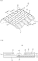
- FIG. 3 is a perspective view of the flexible printed circuit 20
- FIG. 4A is a cross-sectional view taken along line A-A of FIG. 3
- FIG. 4B is a cross-sectional view taken along line B-B of FIG. 3 .
- FIG. 3 shows the flexible printed circuit board 20 before the slots 83 are formed therein. Positions of the slots 83 are indicated by dotted lines in FIG. 3 .
- the flexible printed circuit board 20 includes a base film 31 and wiring patterns.
- the base film 31 is made of an insulating material.
- the bottom face of the base film 31 is bonded to the top face of the rear block 10 and the top face thereof is opposite to the bottom face.
- the wiring patterns are divided into a central wiring pattern 33, a first wiring pattern 35 and a second wiring pattern 37 and formed on both sides of the base film 31.
- the central wiring pattern 33 is formed on the top face of the base film 31 and includes a central pad 43 formed in the region between neighboring second holes 53.
- the central wiring pattern 33 is connected to the central pad 43 through a via 39 and extended to the outside of the rear block 10 through the bottom face of the base film 31.
- the central wiring pattern 33 is alternately arranged on one side and the other side of the central pad 43. Accordingly, the central wiring pattern 33 shown in FIG. 4A is located at the right side of the central pad 43 while the central wiring pattern 33 shown in FIG. 4B is formed at the left side of the central pad 43.
- the first wiring pattern 35 includes a first pad 45 formed at one side of the central pad 43, is connected to the first pad 45 and arranged at one side of the top face of the base film 31.
- the second wiring pattern 37 includes a second pad 47 formed at the other side of the central pad 43, is connected to the second pad 47 and arranged at the other side of the top face of the base film 31.
- a protective layer 41 for protecting the wiring patterns is formed on the bottom face of the central wiring pattern 33 and the top faces of the first and second wiring patterns 35 and 37.
- the central pad 43, the first pad 45 and the second pad 47 are not protected by the protective layer 41 and they are exposed to be connected to the lower electrode 57 of the piezoelectric wafer 50.
- a ground layer 49 is formed on the protective layer 41 formed on the first and second wiring patterns 35 and 37 and connected to the ground electrode plate 60.
- the flexible printed circuit board 20 has the three wiring patterns including the central wiring pattern 33, the first wiring pattern 35 and the second wiring pattern 37, the number of wiring patterns is not limited thereto. If five wiring patterns are formed, the central wiring pattern is alternately formed on one side and the other side of the bottom face of the base film, two wiring patterns are formed on one side of the central wiring pattern and the other two wiring patterns are formed on the other side of the central wiring pattern. The two wiring patterns are respectively arranged at both ends of the flexible printed circuit board.
- a 1.5D (Dimension) ultrasonic probe has a multi-level circuit structure in order to connect circuits on both ends of the ultrasonic probe.
- the vibration and acoustic properties of the ultrasonic probe 100 increases as the thicknesses of the rear block 10, the piezoelectric wafer 50 and the acoustic matching layer 70, the flexible printed circuit 20 and the ground electrode plate 60 decreases.
- circuits on both sides of the flexible printed circuit board 20 according to the present invention are not connected at the contact portion of the flexible printed circuit board 20 and the piezoelectric wafer 50 and both ends of the flexible printed circuit board 20 are bonded to each other, as shown in FIG. 2B , and thus the thickness of the flexible printed circuit board 20 coming into contact with the piezoelectric wafer 50 decreases to improve the acoustic property of the ultrasonic probe 100.
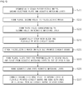
- FIG. 5 is a flowchart showing the method of fabricating the ultrasonic probe according to the first embodiment and FIG. 6 illustrates a method of forming the slots of the ultrasonic probe according to the first embodiment.
- step S711 the piezoelectric wafer 50, the ground electrode plate 60 and the acoustic matching layer 70 are sequentially stacked in step S711.
- the plurality of second holes 53 are formed in the piezoelectric wafer 50 in step S713.
- the rear block 10 and the flexible printed circuit board 20 are sequentially stacked in step S715.
- the piezoelectric wafer 50 stacked in step S711, is located on the top face of the flexible printed circuit board 20, stacked in step S715, in step S721.
- the plurality of slots 83 are formed such that the plurality of slots 83 range from the acoustic matching layer 70 to the top of the rear block 10 in the direction perpendicular to the second holes 53 in step S723.
- the acoustic lens (not shown) is bonded onto the acoustic matching layer 70 having the slots 83 formed therein to cover the overall surface of the acoustic matching layer 70 in step S725.
- the acoustic lens is formed of a material such as silicon and bonded onto the acoustic matching layer 70 using a silicon primer.
- the ground electrode plate 60 is connected to the ground layer 59 of the flexible printed circuit board 20 and both ends of the flexible printed circuit board 20 are bonded to each other to connect the first and second wiring patterns 45 and 55 to construct a circuit in step S727.
- the slots 83 are formed in the rear block 10, the flexible printed circuit board 20, the piezoelectric wafer 50, the ground electrode plate 60 and the acoustic matching layer 70, stacked in step S723, using a dicing machine 500.
- FIG. 6 shows that four of five slots 83 are formed.
- the dicing machine 500 used in step S723 can be used to form the second holes 53 in the piezoelectric wafer 50.
- the ultrasonic probe is bonded using general epoxy in the stacking and bonding steps because electrical bonding can be achieved by coating the general epoxy thin by 1 to 2 ⁇ m. While the general epoxy substitutes for a conductive epoxy having relatively weak adhesiveness, the adhesive used to bond the ultrasonic probe is not limited to the general epoxy.
- FIG. 7 is a cross-sectional view of the ultrasonic probe 200 according to the second embodiment of the present invention
- FIG. 8 is a flowchart showing a method of fabricating the ultrasonic probe 200 according to the second embodiment.
- the ultrasonic probe 200 according to the second embodiment includes a plurality of downwardly extended spaces 113 formed in the rear block 10 and extended downwardly from the respective second holes 53 formed in the piezoelectric wafer 50.
- the number of first holes 113 equals the number of second holes 53.
- the ultrasonic probe 200 according to the second embodiment can reduce ultrasonic interference and improve vibration property according to the downwardly extended spaces 113 formed in the rear block 10.
- the piezoelectric wafer 50, the ground electrode plate 60 and the acoustic matching layer 70 are sequentially stacked in step S611.
- the plurality of second holes 53 are formed in the piezoelectric wafer 50 in step S613 and the first holes 113 corresponding to the second holes 53 are formed in the rear block 10 in step S617.
- the rear block 10 having the first holes 113 formed therein and the flexible printed circuit board 20 are sequentially stacked in step S619. Here, it is more desirable to form the first holes 113 in the rear block 10 and then stack the flexible printed circuit board 20 on the rear block 10.
- the piezoelectric wafer 50 arranged in step S611, is stacked on the flexible printed circuit board 20, placed on the rear block 10 in step S619, in step S621.
- the slots (83 in FIG. 2B ) perpendicular to the second holes 53 are formed such that the slots range from the acoustic matching layer 70 to the top of the rear block 10 in step S623.
- the acoustic lens (not shown) is bonded onto the acoustic matching layer 70 having the slots formed therein to cover the overall surface of the acoustic matching layer 70 in step S625.
- the ground electrode plate 60 is connected to a ground layer (not shown) of the flexible printed circuit board 20 and both ends of the flexible printed circuit board 20 are bonded to each other to connect first and second wiring patterns (not shown) to thereby construct a circuit in step S627.
- FIG. 9 is a cross-sectional view of the ultrasonic probe 300 according to the third embodiment
- FIG. 10 is a flowchart showing a method of fabricating the ultrasonic probe 300 according to the third embodiment.
- the ultrasonic probe 300 according to the third embodiment includes the second holes 53 formed in the piezoelectric wafer 50 and a plurality of third holes 273 formed in the acoustic matching layer 70 and extended upwardly from the second holes 53.
- the number of second holes 53 equals the number of third holes 273.
- the ultrasonic probe 300 according to the third embodiment of the present invention reduces ultrasonic interference according to the second holes 273 formed in the acoustic matching layer 70 to improve vibration property.
- the piezoelectric wafer 50, the ground electrode plate 60 and the acoustic matching layer 70 are sequentially stacked in step S511.
- the plurality of second holes 53 are formed in the piezoelectric wafer 50 in step S513 and the third holes 273 corresponding to the second holes 53 are formed in the acoustic matching layer 70 in step S515.
- the piezoelectric wafer 50 arranged in step S511, is stacked on the flexible printed circuit board 20, placed on the rear block 10 in step S519, in step S521.
- the slots (83 in FIG. 2B ) perpendicular to the second holes 53 are formed such that the slots range from the acoustic matching layer 70 to the top of the rear block 10 in step S523.
- the acoustic lens (not shown) is bonded onto the acoustic matching layer 70 having the slots formed therein to cover the overall surface of the acoustic matching layer 70 in step S525.
- the ground electrode plate 60 is connected to a ground layer (not shown) of the flexible printed circuit board 20 and both ends of the flexible printed circuit board 20 are bonded to each other to connect first and second wiring patterns (not shown) to thereby construct a circuit in step S527.
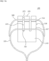
- FIG. 11A is a cross-sectional view of the ultrasonic probe 400 according to the fourth embodiment
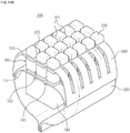
- FIG. 11B is a perspective view of the ultrasonic probe 400 according to the fourth embodiment
- FIG. 12 is a flowchart showing a method of fabricating the ultrasonic probe 400 according to the fourth embodiment.
- the ultrasonic probe 400 according to the fourth embodiment includes the downwardly extended spaces 113 formed in the rear block 10, the second holes 53 formed in the piezoelectric wafer 50 and the third holes 273 formed in the acoustic matching layer 70.
- the number of first holes 113, the number of second holes 53 and the number of third holes 273 are identical.
- the ultrasonic probe 400 according to the fourth embodiment can minimize inter-layer interference according to the second holes 53 formed in the piezoelectric wafer 50 and their extended holes 113 and 273 respectively formed in the rear block 10 and the acoustic matching layer 70 to improve vibration property.
- the piezoelectric wafer 50, the ground electrode plate 60 and the acoustic matching layer 70 are sequentially stacked in step S411.
- the plurality of second holes 53 are formed in the piezoelectric wafer 50 in step S413 and the third holes 273 corresponding to the second holes 53 are formed in the acoustic matching layer 70 in step S415.
- the first holes 113 corresponding to the second holes 53 are formed in the upper part of the rear block 10 in step S417.
- the rear block 10 having the first holes 113 formed therein and the flexible printed circuit board 20 are sequentially stacked in step S419.
- the piezoelectric wafer 50 arranged in step S411, is stacked on the flexible printed circuit board 20, placed on the rear block 10 in step S419, in step S421.
- the slots 83 perpendicular to the second holes 53 are formed such that the slots 83 range from the acoustic matching layer 70 to the top of the rear block 10 in step S423.
- the acoustic lens (not shown) is bonded onto the acoustic matching layer 70 having the slots 83 formed therein to cover the overall surface of the acoustic matching layer 70 in step S425.
- the ground electrode plate 60 is connected to the ground layer of the flexible printed circuit board 20 and both ends of the flexible printed circuit board 20 are bonded to each other to connect first and second wiring patterns (not shown) to thereby construct a circuit in step S427.
Landscapes
- Health & Medical Sciences (AREA)
- Life Sciences & Earth Sciences (AREA)
- Engineering & Computer Science (AREA)
- Pathology (AREA)
- General Health & Medical Sciences (AREA)
- Physics & Mathematics (AREA)
- Molecular Biology (AREA)
- Veterinary Medicine (AREA)
- Radiology & Medical Imaging (AREA)
- Biomedical Technology (AREA)
- Heart & Thoracic Surgery (AREA)
- Medical Informatics (AREA)
- Biophysics (AREA)
- Surgery (AREA)
- Animal Behavior & Ethology (AREA)
- Nuclear Medicine, Radiotherapy & Molecular Imaging (AREA)
- Public Health (AREA)
- Mechanical Engineering (AREA)
- Gynecology & Obstetrics (AREA)
- Chemical & Material Sciences (AREA)
- Analytical Chemistry (AREA)
- Biochemistry (AREA)
- General Physics & Mathematics (AREA)
- Immunology (AREA)
- Ultra Sonic Daignosis Equipment (AREA)
- Transducers For Ultrasonic Waves (AREA)
- Investigating Or Analyzing Materials By The Use Of Ultrasonic Waves (AREA)
Description
- The present invention relates to the field of ultrasonics. and is defined in the claims.Other embodiments are merely exemplary.
- Embodiments relate to an ultrasonic probe, an ultrasonic imaging apparatus and a fabricating method thereof, and more particularly, to an ultrasonic probe, an ultrasonic imaging apparatus and a fabricating method thereof for enhancing vibration property and improving focusing of ultrasonic images to obtain clear images.
- Ultrasound is a method of examining tissues of the human body using ultrasonic waves, which irradiates ultrasonic waves to an affected area of the human body and detects an abnormal tissue through an image generated from a reflected signal. The ultrasound is used to diagnose lesions such as a tumor or test embryos.
- Ultrasonic waves are defined as sound having a frequency higher than a frequency range that people can hear, generally, 20,000Hz to 30MHz. Ultrasonic waves for diagnosis of the human body are in the range of 1 MHz to 20MHz.
- An ultrasonic imaging apparatus used for ultrasound may be divided into three parts, that is, an ultrasonic probe, a signal processor and a display. The ultrasonic probe converts electric and ultrasonic signals and the signal processor processes receiving signals and transmitting signals. The display generates images using signals obtained from the ultrasonic probe and the signal processor. Particularly, the ultrasonic probe is an important part that determines the quality of an ultrasonic image.
- The ultrasonic probe includes a piezoelectric wafer, an electrode, an acoustic matching layer, a printed circuit board and an acoustic lens, in general. The size of the ultrasonic probe is decreasing, which requires a method of arranging wiring patterns for processing ultrasonic and electric signals in the ultrasonic probe and a technique for improving vibration property and focusing to obtain clear ultrasonic images and widen a signal bandwidth.
- Embodiments of the present invention provide an ultrasonic probe, an ultrasonic imaging apparatus and a fabricating method thereof for enhancing the vibration property of the ultrasonic imaging apparatus an improving focusing of ultrasonic images to obtain clear images.
- In one aspect, there is provided an ultrasonic probe including a rear block having a predetermined thickness, a flexible printed circuit board stacked on the rear block to surround the top face and side of the rear block and having wiring patterns formed thereon, a piezoelectric wafer stacked on the top face of the flexible printed circuit board and having upper and lower electrodes respectively formed on both sides thereof and a plurality of second holes formed therein, a ground electrode plate stacked on the top face of the piezoelectric wafer, bonded to the upper electrode and connected to a ground layer of the flexible printed circuit board, an acoustic matching layer stacked on the top face of the ground electrode plate, an acoustic lens bonded onto the acoustic matching layer, and a plurality of slots formed in the direction perpendicular to the second holes and ranging from in the acoustic matching layer to the top of the rear block.
- In an embodiment, the flexible printed circuit board includes a base film formed of an insulating material and having a bottom face bonded onto the rear block and a top face opposite to the bottom face, and wiring patterns formed on both sides of the base film. The wiring patterns includes a central wiring pattern that is formed on the top face of the base film, has a central pad formed between neighboring second holes, is connected to the central pad through a via and is extended to the outside of the rear block through the bottom face of the base film, a first wiring pattern that has a first pad formed at one side of the central pad, is connected to the first pad and is arranged at one side of the top face of the base film, a second wiring pattern that has second pad formed on the other side of the central pad, is connected to the second pad and is arranged at the other side of the top face of the base film, a protective layer formed on the bottom face of the central wiring pattern and the top faces of the first and second wiring patterns to protect the central wiring pattern, the first and second wiring patterns, and a ground layer formed on the protective layer formed on the top faces of the first and second wiring patterns and connected to the ground electrode plate.
- In another aspect, there is provided an ultrasonic imaging apparatus includes the ultrasonic probe and a main body having a connector connected to the ultrasonic probe.
- In yet another aspect, there is provided a method of fabricating an ultrasonic probe, which includes a first stacking step of sequentially stacking a piezoelectric wafer, a ground electrode plate and an acoustic matching layer, a second hole forming step of forming a plurality of second holes in the piezoelectric wafer, a second stacking step of sequentially stacking a rear block and a flexible printed circuit board, a third stacking step of stacking the piezoelectric wafer on the flexible printed circuit board, a slot forming step of forming a plurality of slots perpendicular to the second holes such that the slots range from the acoustic matching layer to the top of the rear block, and a bonding step of bonding an acoustic lens onto the acoustic matching layer.
- Holes may be formed in at least one of the rear block, the piezoelectric wafer and the acoustic matching layer and a plurality of slots are formed through a one-time dicing process such that the slots range from the acoustic matching layer to the top of the rear block to form a wiring patterns in the form of a matrix array. Accordingly, the vibration property and focusing can be improved to obtain clear images.
- Furthermore, the present invention reduces ultrasonic signal interference and provides a wide bandwidth and high sensitivity.
- Moreover, a wiring pattern is arranged in the form of a matrix array to control ultrasonic signals or power used for ultrasound, and thus it is possible to adjust a focusing depth, extend an ultrasound area and obtain clear images.
- In addition, the connector that connects the ultrasonic probe to the main body of the ultrasonic imaging apparatus is located on the top of the main body, and thus users can use the ultrasonic imaging apparatus conveniently.
- The above and other features and advantages of the present invention will become more apparent by describing in detail exemplary embodiments thereof with reference to the attached drawings in which:
-
FIG. 1 illustrates an ultrasonic imaging apparatus according to a first embodiment of the present invention; -
FIG. 2A is a cross-sectional view of an ultrasonic probe according to the first embodiment of the present invention; -
FIG. 2B is a perspective view of the ultrasonic probe according to the first embodiment of the present invention; -
FIG. 3 is a perspective view of a flexible printed circuit board according to an embodiment of the present invention; -
FIG. 4A is a cross-sectional view taken along line A-A ofFIG. 3 ; -
FIG. 4B is a cross-sectional view taken along line B-B ofFIG. 3 ; -
FIG. 5 is a flowchart showing a method of fabricating the ultrasonic probe according to the first embodiment; -
FIG. 6 illustrates a method of forming slots of the ultrasonic probe according to the first embodiment; -
FIG. 7 is a cross-sectional view of an ultrasonic probe according to a second embodiment; -
FIG. 8 is a flowchart showing a method of fabricating the ultrasonic probe according to the second embodiment; -
FIG. 9 is a cross-sectional view of an ultrasonic probe according to a third embodiment; -
FIG. 10 is a flowchart showing a method of fabricating the ultrasonic probe according to the third embodiment; -
FIG. 11A is a cross-sectional view of an ultrasonic probe according to a fourth embodiment; -
FIG. 11B is a perspective view of the ultrasonic probe according to the fourth embodiment; and -
FIG. 12 is a flowchart showing a method of fabricating the ultrasonic probe according to the fourth embodiment. - The present invention will now be described more fully with reference to the accompanying drawings, in which exemplary embodiments of the invention are shown. Throughout the drawings, like reference numerals refer to like elements.
- Referring to
FIG. 1 , the ultrasonic imaging apparatus 1 includes amain body 11, anultrasonic probe 100, adisplay 13 and aninput unit 14. - The
main body 11 includes a signal processor that transmits and receives electric and ultrasonic signals and a storage unit that stores application programs and data required for ultrasound. Further, aconnector 15 for connecting theultrasonic probe 100 to themain body 11 is provided outside themain body 11. Theconnector 15 is placed on the top of themain body 11 such that a user can easily connect theultrasonic probe 100 to themain body 11. - The
ultrasonic probe 100 includes anacoustic lens 80 coming into contact with an affected area of a patient and acase 90 covering the other components of theultrasonic probe 100. Theacoustic lens 80 is used for focusing an ultrasonic image and arranged to cover an acoustic matching layer placed under theacoustic lens 80. Theacoustic lens 80 may be made of silicon. The other components of theultrasonic probe 100, covered with thecase 90, will be explained in detail later. - The
display 13 displays ultrasonic images obtained through application programs executed for ultrasound and examination. - The
input unit 14 is used to execute the application programs or input data required for examination and includes a plurality of keys. - The
ultrasonic probe 100 according to the first embodiment of the present invention will now be explained with reference toFIGS. 2A and2B .FIG. 2A is a cross-sectional view of theultrasonic probe 100 according to the first embodiment of the present invention andFIG. 2B is a perspective view of theultrasonic probe 100 according to the first embodiment of the present invention. - The
ultrasonic probe 100 according to the first embodiment of the present invention includes arear block 10, a flexible printedcircuit board 20, apiezoelectric wafer 50, aground electrode plate 60 and anacoustic matching layer 70, which are sequentially stacked. While theultrasonic probe 100 according to the first embodiment of the present invention includes the acoustic lens 80 (shown inFIG. 1 ) placed on theacoustic matching layer 70, the acoustic lens is not shown inFIGS. 2A and2B . - The
rear block 10 is located at the bottom of theultrasonic probe 100 and absorbs unnecessary ultrasonic signals traveling to therear block 10 from thepiezoelectric wafer 50. - The flexible printed
circuit board 20 is located on the top face of therear block 10 and has wiring patterns formed on both sides thereof. The flexible printedcircuit board 20 will be explained in more detail later. - The
piezoelectric wafer 50 is arranged on the top face of the flexible printedcircuit board 20. Thepiezoelectric wafer 50 has upper andlower electrodes second holes 53. - While two
second holes 53 are formed in thepiezoelectric wafer 50 in the first embodiment of the present invention, the number ofsecond holes 53 is not limited thereto. Thepiezoelectric wafer 50 may be formed of PZT or PMN-PT. The upper andlower electrodes upper electrode 55 is connected to theground electrode plate 60 and thelower electrode 57 is connected to the flexible printedcircuit board 20. - The
ground electrode plate 60 has a metal layer formed on the top face thereof and an insulating layer formed on the bottom face thereof and surrounds the top face and the side of thepiezoelectric wafer 50. The flexible printedcircuit board 20 includes a ground layer. The bottom end of theground electrode plate 60 is connected to the ground layer of the flexible printedcircuit board 20. - The
acoustic matching layer 70 is made of metal powder or ceramic powder and formed on the top face of theground electrode plate 60. - A plurality of
slots 83 are formed such that the plurality ofslots 83 range from theacoustic matching layer 70 to the top of therear block 10 in the direction perpendicular to the second holes 53. While theultrasonic probe 100 according to the first embodiment of the present invention has fiveslots 83, the number ofslots 83 is not limited thereto. - The acoustic lens (not shown) is used for focusing ultrasonic images and located on the top face of the
acoustic matching layer 70. - The flexible printed
circuit board 20 and the wiring patterns according to the first embodiment of the present invention will now be explained with reference toFIGS. 2A ,2B ,3, 4A and4B .FIG. 3 is a perspective view of the flexible printedcircuit 20,FIG. 4A is a cross-sectional view taken along line A-A ofFIG. 3 andFIG. 4B is a cross-sectional view taken along line B-B ofFIG. 3 . -
FIG. 3 shows the flexible printedcircuit board 20 before theslots 83 are formed therein. Positions of theslots 83 are indicated by dotted lines inFIG. 3 . - Referring to
FIGS. 2A ,2B ,3, 4A and4B , the flexible printedcircuit board 20 includes abase film 31 and wiring patterns. Thebase film 31 is made of an insulating material. The bottom face of thebase film 31 is bonded to the top face of therear block 10 and the top face thereof is opposite to the bottom face. The wiring patterns are divided into acentral wiring pattern 33, afirst wiring pattern 35 and asecond wiring pattern 37 and formed on both sides of thebase film 31. - The
central wiring pattern 33 is formed on the top face of thebase film 31 and includes acentral pad 43 formed in the region between neighboring second holes 53. Thecentral wiring pattern 33 is connected to thecentral pad 43 through a via 39 and extended to the outside of therear block 10 through the bottom face of thebase film 31. Here, thecentral wiring pattern 33 is alternately arranged on one side and the other side of thecentral pad 43. Accordingly, thecentral wiring pattern 33 shown inFIG. 4A is located at the right side of thecentral pad 43 while thecentral wiring pattern 33 shown inFIG. 4B is formed at the left side of thecentral pad 43. - The
first wiring pattern 35 includes afirst pad 45 formed at one side of thecentral pad 43, is connected to thefirst pad 45 and arranged at one side of the top face of thebase film 31. Thesecond wiring pattern 37 includes asecond pad 47 formed at the other side of thecentral pad 43, is connected to thesecond pad 47 and arranged at the other side of the top face of thebase film 31. - A
protective layer 41 for protecting the wiring patterns is formed on the bottom face of thecentral wiring pattern 33 and the top faces of the first andsecond wiring patterns central pad 43, thefirst pad 45 and thesecond pad 47 are not protected by theprotective layer 41 and they are exposed to be connected to thelower electrode 57 of thepiezoelectric wafer 50. - A
ground layer 49 is formed on theprotective layer 41 formed on the first andsecond wiring patterns ground electrode plate 60. - While the
central pad 43, thefirst pad 45 and thesecond pad 47 form a 3X6 matrix array in the flexible printedcircuit board 20 according to the first embodiment of the present invention, they can form 3X64 through 3X192 matrix arrays. - Furthermore, while the flexible printed
circuit board 20 according to the first embodiment of the present invention has the three wiring patterns including thecentral wiring pattern 33, thefirst wiring pattern 35 and thesecond wiring pattern 37, the number of wiring patterns is not limited thereto. If five wiring patterns are formed, the central wiring pattern is alternately formed on one side and the other side of the bottom face of the base film, two wiring patterns are formed on one side of the central wiring pattern and the other two wiring patterns are formed on the other side of the central wiring pattern. The two wiring patterns are respectively arranged at both ends of the flexible printed circuit board. - In general, circuit connection is achieved at a contact portion of the
piezoelectric wafer 50 and the flexible printedcircuit board 20. A 1.5D (Dimension) ultrasonic probe has a multi-level circuit structure in order to connect circuits on both ends of the ultrasonic probe. However, the vibration and acoustic properties of theultrasonic probe 100 increases as the thicknesses of therear block 10, thepiezoelectric wafer 50 and theacoustic matching layer 70, the flexible printedcircuit 20 and theground electrode plate 60 decreases. Accordingly, circuits on both sides of the flexible printedcircuit board 20 according to the present invention are not connected at the contact portion of the flexible printedcircuit board 20 and thepiezoelectric wafer 50 and both ends of the flexible printedcircuit board 20 are bonded to each other, as shown inFIG. 2B , and thus the thickness of the flexible printedcircuit board 20 coming into contact with thepiezoelectric wafer 50 decreases to improve the acoustic property of theultrasonic probe 100. - A method of fabricating the ultrasonic probe according to the first embodiment will now be explained with reference to
FIGS. 2 through 6 .FIG. 5 is a flowchart showing the method of fabricating the ultrasonic probe according to the first embodiment andFIG. 6 illustrates a method of forming the slots of the ultrasonic probe according to the first embodiment. - Referring to
FIG. 5 , thepiezoelectric wafer 50, theground electrode plate 60 and theacoustic matching layer 70 are sequentially stacked in step S711. - The plurality of
second holes 53 are formed in thepiezoelectric wafer 50 in step S713. - The
rear block 10 and the flexible printedcircuit board 20 are sequentially stacked in step S715. - The
piezoelectric wafer 50, stacked in step S711, is located on the top face of the flexible printedcircuit board 20, stacked in step S715, in step S721. - When the
rear block 10, the flexible printedcircuit board 20, thepiezoelectric wafer 50, theground electrode plate 60 and theacoustic matching layer 70 are sequentially stacked, the plurality ofslots 83 are formed such that the plurality ofslots 83 range from theacoustic matching layer 70 to the top of therear block 10 in the direction perpendicular to thesecond holes 53 in step S723. - The acoustic lens (not shown) is bonded onto the
acoustic matching layer 70 having theslots 83 formed therein to cover the overall surface of theacoustic matching layer 70 in step S725. The acoustic lens is formed of a material such as silicon and bonded onto theacoustic matching layer 70 using a silicon primer. - The
ground electrode plate 60 is connected to the ground layer 59 of the flexible printedcircuit board 20 and both ends of the flexible printedcircuit board 20 are bonded to each other to connect the first andsecond wiring patterns - The method of forming the
slots 83 in step S723 will now be explained with reference toFIG. 6 . - Referring to
FIG. 6 , theslots 83 are formed in therear block 10, the flexible printedcircuit board 20, thepiezoelectric wafer 50, theground electrode plate 60 and theacoustic matching layer 70, stacked in step S723, using a dicingmachine 500.FIG. 6 shows that four of fiveslots 83 are formed. - The dicing
machine 500 used in step S723 can be used to form thesecond holes 53 in thepiezoelectric wafer 50. - The ultrasonic probe is bonded using general epoxy in the stacking and bonding steps because electrical bonding can be achieved by coating the general epoxy thin by 1 to 2µm. While the general epoxy substitutes for a conductive epoxy having relatively weak adhesiveness, the adhesive used to bond the ultrasonic probe is not limited to the general epoxy.
- An
ultrasonic probe 200 according to a second embodiment will now be explained with reference toFIGS. 7 and8 .FIG. 7 is a cross-sectional view of theultrasonic probe 200 according to the second embodiment of the present invention andFIG. 8 is a flowchart showing a method of fabricating theultrasonic probe 200 according to the second embodiment. - The
ultrasonic probe 200 according to the second embodiment includes a plurality of downwardlyextended spaces 113 formed in therear block 10 and extended downwardly from the respectivesecond holes 53 formed in thepiezoelectric wafer 50. The number offirst holes 113 equals the number ofsecond holes 53. Theultrasonic probe 200 according to the second embodiment can reduce ultrasonic interference and improve vibration property according to the downwardlyextended spaces 113 formed in therear block 10. - Referring to
FIGS. 7 and8 , thepiezoelectric wafer 50, theground electrode plate 60 and theacoustic matching layer 70 are sequentially stacked in step S611. The plurality ofsecond holes 53 are formed in thepiezoelectric wafer 50 in step S613 and thefirst holes 113 corresponding to thesecond holes 53 are formed in therear block 10 in step S617. - The
rear block 10 having thefirst holes 113 formed therein and the flexible printedcircuit board 20 are sequentially stacked in step S619. Here, it is more desirable to form thefirst holes 113 in therear block 10 and then stack the flexible printedcircuit board 20 on therear block 10. - The
piezoelectric wafer 50, arranged in step S611, is stacked on the flexible printedcircuit board 20, placed on therear block 10 in step S619, in step S621. - The slots (83 in
FIG. 2B ) perpendicular to thesecond holes 53 are formed such that the slots range from theacoustic matching layer 70 to the top of therear block 10 in step S623. - The acoustic lens (not shown) is bonded onto the
acoustic matching layer 70 having the slots formed therein to cover the overall surface of theacoustic matching layer 70 in step S625. - The
ground electrode plate 60 is connected to a ground layer (not shown) of the flexible printedcircuit board 20 and both ends of the flexible printedcircuit board 20 are bonded to each other to connect first and second wiring patterns (not shown) to thereby construct a circuit in step S627. - An
ultrasonic probe 300 according to a third embodiment will now be explained with reference toFIGS. 9 and10 .FIG. 9 is a cross-sectional view of theultrasonic probe 300 according to the third embodiment andFIG. 10 is a flowchart showing a method of fabricating theultrasonic probe 300 according to the third embodiment. - The
ultrasonic probe 300 according to the third embodiment includes thesecond holes 53 formed in thepiezoelectric wafer 50 and a plurality ofthird holes 273 formed in theacoustic matching layer 70 and extended upwardly from the second holes 53. Here, the number ofsecond holes 53 equals the number ofthird holes 273. Theultrasonic probe 300 according to the third embodiment of the present invention reduces ultrasonic interference according to thesecond holes 273 formed in theacoustic matching layer 70 to improve vibration property. - Referring to
FIGS. 9 and10 , thepiezoelectric wafer 50, theground electrode plate 60 and theacoustic matching layer 70 are sequentially stacked in step S511. The plurality ofsecond holes 53 are formed in thepiezoelectric wafer 50 in step S513 and thethird holes 273 corresponding to thesecond holes 53 are formed in theacoustic matching layer 70 in step S515. - The
rear block 10 and the flexible printedcircuit board 20 are sequentially stacked in step S519. - The
piezoelectric wafer 50, arranged in step S511, is stacked on the flexible printedcircuit board 20, placed on therear block 10 in step S519, in step S521. - The slots (83 in
FIG. 2B ) perpendicular to thesecond holes 53 are formed such that the slots range from theacoustic matching layer 70 to the top of therear block 10 in step S523. - The acoustic lens (not shown) is bonded onto the
acoustic matching layer 70 having the slots formed therein to cover the overall surface of theacoustic matching layer 70 in step S525. - The
ground electrode plate 60 is connected to a ground layer (not shown) of the flexible printedcircuit board 20 and both ends of the flexible printedcircuit board 20 are bonded to each other to connect first and second wiring patterns (not shown) to thereby construct a circuit in step S527. - An
ultrasonic probe 400 according to a fourth embodiment will now be explained with reference toFIGS. 11A ,11B and12 .FIG. 11A is a cross-sectional view of theultrasonic probe 400 according to the fourth embodimentFIG. 11B is a perspective view of theultrasonic probe 400 according to the fourth embodiment andFIG. 12 is a flowchart showing a method of fabricating theultrasonic probe 400 according to the fourth embodiment. - The
ultrasonic probe 400 according to the fourth embodiment includes the downwardlyextended spaces 113 formed in therear block 10, thesecond holes 53 formed in thepiezoelectric wafer 50 and thethird holes 273 formed in theacoustic matching layer 70. The number offirst holes 113, the number ofsecond holes 53 and the number ofthird holes 273 are identical. Theultrasonic probe 400 according to the fourth embodiment can minimize inter-layer interference according to thesecond holes 53 formed in thepiezoelectric wafer 50 and theirextended holes rear block 10 and theacoustic matching layer 70 to improve vibration property. - Referring to
FIGS. 11A ,11B and12 , thepiezoelectric wafer 50, theground electrode plate 60 and theacoustic matching layer 70 are sequentially stacked in step S411. The plurality ofsecond holes 53 are formed in thepiezoelectric wafer 50 in step S413 and thethird holes 273 corresponding to thesecond holes 53 are formed in theacoustic matching layer 70 in step S415. Thefirst holes 113 corresponding to thesecond holes 53 are formed in the upper part of therear block 10 in step S417. - The
rear block 10 having thefirst holes 113 formed therein and the flexible printedcircuit board 20 are sequentially stacked in step S419. - The
piezoelectric wafer 50, arranged in step S411, is stacked on the flexible printedcircuit board 20, placed on therear block 10 in step S419, in step S421. - When the
rear block 10, the flexible printedcircuit board 20, thepiezoelectric wafer 50, theground electrode plate 60 and theacoustic matching layer 70 are sequentially stacked in step S421, theslots 83 perpendicular to thesecond holes 53 are formed such that theslots 83 range from theacoustic matching layer 70 to the top of therear block 10 in step S423. - The acoustic lens (not shown) is bonded onto the
acoustic matching layer 70 having theslots 83 formed therein to cover the overall surface of theacoustic matching layer 70 in step S425. - The
ground electrode plate 60 is connected to the ground layer of the flexible printedcircuit board 20 and both ends of the flexible printedcircuit board 20 are bonded to each other to connect first and second wiring patterns (not shown) to thereby construct a circuit in step S427. - The ultrasonic probe, the ultrasonic imaging apparatus and the fabricating method thereof have been described through embodiments
Claims (8)
- An ultrasonic probe comprising:a rear block (10) having a predetermined thickness;a flexible printed circuit board (20) stacked on the rear block (10) to surround the top face and side of the rear block (10) and having wiring patterns formed thereon;a piezoelectric wafer (50) stacked on the top face of the flexible printed circuit board (20) and having upper and lower electrodes (55, 57) respectively formed on top and bottom faces thereof whereby the lower electrodes (57) are arranged on and connected to the top face of the flexible printed circuit board (20);a ground electrode plate (60) stacked on the top face of the piezoelectric wafer (50), bonded to the upper electrodes (55) and connected to a ground layer of the flexible printed circuit board (20);an acoustic matching layer (70) stacked on the top face of the ground electrode plate (60); andan acoustic lens bonded onto the acoustic matching layer (70),wherein the piezoelectric wafer (50) has a plurality of second holes (53) formed therein, and a plurality of slots (83) are formed in the direction perpendicular to the second holes (53) while ranging from the acoustic matching layer (70) to the top of the rear block (10), whereby the piezoelectric wafer (50) is arranged in the form of a matrix array on the top face of the flexible printed circuit board (20),wherein the flexible printed circuit board (20) comprises:a base film (31) formed of an insulating material and having a bottom face bonded onto the rear block (10) and a top face opposite to the bottom face; andwiring patterns formed on both sides of the base film,wherein the wiring patterns comprises:a central wiring pattern (33) that is formed on the top face of the base film (31), has a central pad (43) formed between neighboring second holes is connected to the central pad (43) through a via (39) and is extended to the outside of the rear block (10) through the bottom face of the base film (31);a first wiring pattern (35) that has a first pad (45) formed at one side of the central pad (43), is connected to the first pad (45) and is arranged at one side of the top face of the base film (31);a second wiring pattern (37) that has a second pad (47) formed on the other side of the central pad (43), is connected to the second pad (47) and is arranged at the other side of the top face of the base film (31);a protective layer (41) formed on the bottom face of the central wiring pattern (33) and the top faces of the first and second wiring patterns (35, 37) to protect the central wiring pattern (33), the first and second wiring patterns (35, 37); anda ground layer (49) formed on the protective layer (41) formed on the top faces of the first and second wiring patterns (35, 37) and connected to the ground electrode plate (60),wherein the central pad (43), the first pad (45) and the second pad (47) form a matrix array in the flexible printed circuit board (20) such that the lower electrodes (57) of the piezoelectric wafer (50) are connected to and arranged in the matrix array on the central pad (43), the first pad (45) and the second pad (47) of the flexible printed circuit board (20),wherein the central wiring pattern (33) is alternately arranged on one side and the other side of the base film (31), andwherein both ends of the flexible printed circuit board (20) are bonded to each other such that the first and second wiring patterns (35, 37) are connected to each other.
- The ultrasonic probe of claim 1, wherein the rear block has first holes formed therein, which correspond to the second holes.
- The ultrasonic probe of claim 1, wherein the acoustic matching layer has third holes formed therein, which correspond to the second holes.
- The ultrasonic probe of claim 1, wherein the rear block has first holes formed therein, which correspond to the second holes, and the acoustic matching layer has third holes formed therein, which correspond to the second holes.
- The ultrasonic probe of claim 1, wherein the central pad (43), the first pad and the second pad (45, 47) form a 3X96 matrix array.
- The ultrasonic probe of claim 5, wherein the number of the slots (83) is 95.
- An ultrasonic imaging apparatus comprising:the ultrasonic probe (100, 200, 300, 400) according to one of claims 1 to 6; anda main body (11) having a connector (15) connected to the ultrasonic probe.
- The ultrasonic imaging apparatus of claim 7, wherein the connector (15) is located on the top of the main body (11).
Applications Claiming Priority (1)
| Application Number | Priority Date | Filing Date | Title |
|---|---|---|---|
| KR20090010661A KR101064601B1 (en) | 2009-02-10 | 2009-02-10 | Ultrasonic transducers, ultrasonic imaging devices and methods of manufacturing the same |
Publications (2)
| Publication Number | Publication Date |
|---|---|
| EP2216104A1 EP2216104A1 (en) | 2010-08-11 |
| EP2216104B1 true EP2216104B1 (en) | 2017-02-01 |
Family
ID=42078020
Family Applications (1)
| Application Number | Title | Priority Date | Filing Date |
|---|---|---|---|
| EP10151791.0A Active EP2216104B1 (en) | 2009-02-10 | 2010-01-27 | Ultrasonic probe, ultrasonic imaging apparatus and fabricating method thereof |
Country Status (7)
| Country | Link |
|---|---|
| US (1) | US8547799B2 (en) |
| EP (1) | EP2216104B1 (en) |
| JP (1) | JP5479131B2 (en) |
| KR (1) | KR101064601B1 (en) |
| CN (1) | CN101797166B (en) |
| TW (1) | TWI424596B (en) |
| WO (1) | WO2010093083A1 (en) |
Cited By (1)
| Publication number | Priority date | Publication date | Assignee | Title |
|---|---|---|---|---|
| CN109926298A (en) * | 2017-12-18 | 2019-06-25 | 深圳先进技术研究院 | One mode converts ultrasonic transducer and its manufacturing method |
Families Citing this family (52)
| Publication number | Priority date | Publication date | Assignee | Title |
|---|---|---|---|---|
| JP2011250119A (en) * | 2010-05-26 | 2011-12-08 | Toshiba Corp | Ultrasonic probe |
| CN102528266B (en) * | 2010-12-24 | 2014-03-05 | 中国科学院深圳先进技术研究院 | Welding Method of Circuit Leads of Ultrasonic Array Sound Head Element |
| KR101222911B1 (en) * | 2011-01-14 | 2013-01-16 | 경북대학교 산학협력단 | Two dimensional ultrasonic transducer |
| JP5643667B2 (en) | 2011-01-28 | 2014-12-17 | 株式会社東芝 | Ultrasonic transducer, ultrasonic probe, and method of manufacturing ultrasonic transducer |
| JP5259762B2 (en) * | 2011-03-24 | 2013-08-07 | 株式会社東芝 | Ultrasonic probe and ultrasonic probe manufacturing method |
| WO2013021597A1 (en) * | 2011-08-05 | 2013-02-14 | パナソニック株式会社 | Ultrasound probe and flexible substrate used in ultrasound probe |
| CN102406432B (en) * | 2011-10-12 | 2014-01-08 | 湖北益都电器有限公司 | Multifunctional electric cooker |
| JP6091755B2 (en) * | 2012-01-24 | 2017-03-08 | 東芝メディカルシステムズ株式会社 | Ultrasonic probe and ultrasonic diagnostic apparatus |
| KR101350520B1 (en) * | 2012-02-24 | 2014-01-16 | 경북대학교 산학협력단 | Multi-layer active material type ultrasonic transducer and manufacturing method thereof |
| JP6019671B2 (en) * | 2012-03-30 | 2016-11-02 | セイコーエプソン株式会社 | Ultrasonic probe, electronic device, and ultrasonic diagnostic apparatus |
| JP5746082B2 (en) * | 2012-03-30 | 2015-07-08 | 富士フイルム株式会社 | Ultrasonic probe and signal line connection method |
| KR101336246B1 (en) | 2012-04-23 | 2013-12-03 | 삼성전자주식회사 | Ultrasonic transducer, ultrasonic probe, and ultrasound image diagnosis apparatus |
| KR101419318B1 (en) * | 2012-08-28 | 2014-07-15 | 주식회사 휴먼스캔 | backing block for ultrasound probe and method for preparing of backing block thereof |
| KR101496863B1 (en) * | 2013-05-09 | 2015-03-02 | 주식회사 휴먼스캔 | Separating and binding type ultrasound probe apparatus |
| KR101493670B1 (en) | 2013-05-09 | 2015-02-16 | 주식회사 휴먼스캔 | Ultrasonic porbe, ultrasonic probe module having the same, and ultrasonic porbe apparatus having the ultrasonc probe module |
| KR101491800B1 (en) * | 2013-05-13 | 2015-02-11 | 알피니언메디칼시스템 주식회사 | Method of manufacturing transducer and transducer manufactured thereby |
| CN103300889B (en) * | 2013-05-17 | 2015-04-29 | 深圳市理邦精密仪器股份有限公司 | Ultrasonic array probe signal acquisition component and preparation method thereof, and probe |
| JP6102622B2 (en) * | 2013-08-07 | 2017-03-29 | コニカミノルタ株式会社 | Ultrasonic probe |
| JP6252130B2 (en) * | 2013-11-20 | 2017-12-27 | セイコーエプソン株式会社 | Ultrasonic device, manufacturing method thereof, electronic apparatus, and ultrasonic imaging apparatus |
| KR102092589B1 (en) | 2014-04-23 | 2020-03-24 | 삼성전자주식회사 | Ultrasound Probe and Manufacturing Method thereof |
| GB2528338B (en) * | 2014-11-28 | 2016-07-13 | 168 Ultrasound Pte Ltd | Ultrasound apparatus and method |
| WO2016093115A1 (en) * | 2014-12-12 | 2016-06-16 | 株式会社村田製作所 | Vibrating body and vibrating body array |
| WO2016125040A2 (en) * | 2015-02-06 | 2016-08-11 | Koninklijke Philips N.V. | Systems, methods, and apparatuses for thermal management of ultrasound transducers |
| KR101654298B1 (en) * | 2015-03-12 | 2016-09-05 | (주)엘라켐 | Realtime monitoring system by ultrasonography |
| KR101654296B1 (en) * | 2015-03-12 | 2016-09-05 | (주)엘라켐 | Ultrasonography probe with piezoelectric element |
| CN104800974A (en) * | 2015-04-16 | 2015-07-29 | 修清 | Heart failure treatment device |
| CN105032749A (en) * | 2015-07-09 | 2015-11-11 | 深圳市理邦精密仪器股份有限公司 | Multi-layer lamination ultrasonic transducer and manufacturing method thereof |
| CN105080822A (en) * | 2015-09-07 | 2015-11-25 | 上海爱声生物医疗科技有限公司 | Novel ultrasonic transducer |
| KR101625657B1 (en) * | 2015-10-27 | 2016-05-30 | 알피니언메디칼시스템 주식회사 | Ultrasound probe |
| CN105436065B (en) * | 2015-11-23 | 2017-10-31 | 华中科技大学 | A kind of preparation method of the ultrasonic face battle array probe of ranks addressing |
| JP6791671B2 (en) * | 2015-12-11 | 2020-11-25 | キヤノンメディカルシステムズ株式会社 | Ultrasonic probe |
| EP3437565B8 (en) | 2016-04-01 | 2021-05-26 | FUJIFILM Corporation | Ultrasonic oscillator unit and ultrasonic endoscope using same |
| KR102627726B1 (en) * | 2016-05-10 | 2024-01-23 | 삼성메디슨 주식회사 | Ultrasound Probe |
| KR102227329B1 (en) * | 2016-07-26 | 2021-03-12 | 지멘스 메디컬 솔루션즈 유에스에이, 인크. | Ultrasound transducer and manufacturing method thereof |
| CN106333708B (en) * | 2016-08-22 | 2019-09-13 | 深圳开立生物医疗科技股份有限公司 | A kind of flexible circuit board, transesophageal probe and transesophageal probe preparation method |
| JP6852366B2 (en) * | 2016-11-29 | 2021-03-31 | セイコーエプソン株式会社 | Ultrasonic device and ultrasonic device |
| KR102717595B1 (en) | 2017-02-21 | 2024-10-16 | 삼성메디슨 주식회사 | Ultrasonic probe |
| KR102370812B1 (en) * | 2017-09-13 | 2022-03-07 | 지멘스 메디컬 솔루션즈 유에스에이, 인크. | Ultrasound transducer |
| KR102140864B1 (en) * | 2018-05-31 | 2020-08-03 | 한국교통대학교산학협력단 | Transducers for non contact mid air tactile sensing feedback and Operating method thereof |
| KR102093248B1 (en) | 2018-07-23 | 2020-04-23 | 한국과학기술원 | Ultrasound prove array and fabrication method of thereof |
| CN112839591B (en) * | 2018-10-19 | 2024-11-15 | 奥林巴斯株式会社 | Ultrasonic probes and ultrasonic endoscopes |
| KR102176668B1 (en) | 2018-12-28 | 2020-11-09 | 한국과학기술원 | Ultrasonic probe |
| CN111511109B (en) * | 2019-01-30 | 2021-11-23 | 京东方科技集团股份有限公司 | Flexible circuit board and manufacturing method thereof, electronic device module and electronic device |
| US11500489B2 (en) | 2019-01-30 | 2022-11-15 | Chengdu Boe Optoelectronics Technology Co., Ltd. | Flexible circuit board and manufacturing method, display device, circuit board structure and display panel thereof |
| CN109730654B (en) * | 2019-03-11 | 2024-06-07 | 上海安清医疗器械有限公司 | Detection packaging structure and in-vivo detection device |
| CN113825481B (en) * | 2019-08-14 | 2024-05-14 | 塔科特有限会社 | Vibration generating device |
| CN110772288B (en) * | 2019-12-10 | 2025-09-02 | 深圳先进技术研究院 | Ultrasonic endoscope system and ultrasonic transducer |
| KR102359155B1 (en) | 2019-12-31 | 2022-02-08 | 한국과학기술원 | Hybrid ultrasound prove array and method of manufacturing the same |
| CN111458414B (en) * | 2020-04-24 | 2021-06-15 | 哈尔滨工业大学 | Ultrasonic phased array transducer device with one-dimensional hinge array structure |
| KR102623559B1 (en) * | 2021-02-10 | 2024-01-11 | 주식회사 에프씨유 | Ultrasound prove |
| JP7106782B1 (en) * | 2022-05-19 | 2022-07-26 | 株式会社日立パワーソリューションズ | ULTRASOUND IMAGING DEVICE AND METHOD FOR PREVENTING LIQUID INTEGRATION TO BONDED WAFER |
| CN117115869B (en) * | 2023-08-23 | 2025-02-07 | 汇科(新加坡)控股私人有限公司 | Acoustic layer preparation method, ultrasonic chip and ultrasonic fingerprint module |
Family Cites Families (19)
| Publication number | Priority date | Publication date | Assignee | Title |
|---|---|---|---|---|
| US4217684A (en) * | 1979-04-16 | 1980-08-19 | General Electric Company | Fabrication of front surface matched ultrasonic transducer array |
| JPH0523331A (en) * | 1991-07-19 | 1993-02-02 | Fujitsu Ltd | Ultrasonic probe and method for manufacturing piezoelectric vibrator plate used for the probe |
| JP3277013B2 (en) * | 1993-03-04 | 2002-04-22 | 株式会社東芝 | Ultrasonic probe device and manufacturing method thereof |
| JP3325368B2 (en) * | 1993-11-08 | 2002-09-17 | 株式会社東芝 | Ultrasonic probe and manufacturing method thereof |
| JP3526486B2 (en) * | 1995-04-28 | 2004-05-17 | 株式会社東芝 | Ultrasonic probe, ultrasonic probe equipped with the probe, and methods of manufacturing these |
| US5810009A (en) * | 1994-09-27 | 1998-09-22 | Kabushiki Kaisha Toshiba | Ultrasonic probe, ultrasonic probe device having the ultrasonic probe, and method of manufacturing the ultrasonic probe |
| JP3384889B2 (en) * | 1994-10-21 | 2003-03-10 | ジーイー横河メディカルシステム株式会社 | Ultrasonic probe |
| US5598051A (en) * | 1994-11-21 | 1997-01-28 | General Electric Company | Bilayer ultrasonic transducer having reduced total electrical impedance |
| JP3378727B2 (en) * | 1996-05-31 | 2003-02-17 | 株式会社日立メディコ | Probe for ultrasonic diagnostic equipment |
| JPH11155859A (en) * | 1997-09-24 | 1999-06-15 | Toshiba Corp | Ultrasonic probe and ultrasonic diagnostic apparatus using the same |
| US6894425B1 (en) * | 1999-03-31 | 2005-05-17 | Koninklijke Philips Electronics N.V. | Two-dimensional ultrasound phased array transducer |
| JP4936597B2 (en) * | 2000-02-07 | 2012-05-23 | 株式会社東芝 | Ultrasonic probe and ultrasonic probe manufacturing method |
| US6640634B2 (en) * | 2000-03-31 | 2003-11-04 | Kabushiki Kaisha Toshiba | Ultrasonic probe, method of manufacturing the same and ultrasonic diagnosis apparatus |
| US7053530B2 (en) * | 2002-11-22 | 2006-05-30 | General Electric Company | Method for making electrical connection to ultrasonic transducer through acoustic backing material |
| JP2007228719A (en) * | 2006-02-23 | 2007-09-06 | Toshiba Corp | Hybrid power generation element, power supply device using hybrid power generation element, and method of installing hybrid power generation element |
| JP4860351B2 (en) * | 2006-05-22 | 2012-01-25 | 富士フイルム株式会社 | Curved surface attaching method and ultrasonic probe |
| JP2008085413A (en) * | 2006-09-26 | 2008-04-10 | Nippon Dempa Kogyo Co Ltd | Ultrasonic probe and manufacturing method thereof |
| JP2008085537A (en) | 2006-09-27 | 2008-04-10 | Fujifilm Corp | Ultrasound probe |
| JP5038865B2 (en) * | 2007-11-22 | 2012-10-03 | 株式会社東芝 | Ultrasonic probe, ultrasonic diagnostic apparatus, and method of manufacturing ultrasonic probe |
-
2009
- 2009-02-10 KR KR20090010661A patent/KR101064601B1/en active Active
- 2009-03-30 WO PCT/KR2009/001613 patent/WO2010093083A1/en not_active Ceased
-
2010
- 2010-01-27 EP EP10151791.0A patent/EP2216104B1/en active Active
- 2010-01-28 JP JP2010017231A patent/JP5479131B2/en active Active
- 2010-02-03 US US12/699,166 patent/US8547799B2/en active Active
- 2010-02-09 CN CN201010116730XA patent/CN101797166B/en active Active
- 2010-02-10 TW TW99104150A patent/TWI424596B/en active
Non-Patent Citations (1)
| Title |
|---|
| None * |
Cited By (2)
| Publication number | Priority date | Publication date | Assignee | Title |
|---|---|---|---|---|
| CN109926298A (en) * | 2017-12-18 | 2019-06-25 | 深圳先进技术研究院 | One mode converts ultrasonic transducer and its manufacturing method |
| CN109926298B (en) * | 2017-12-18 | 2021-01-05 | 深圳先进技术研究院 | Mode conversion ultrasonic transducer and manufacturing method thereof |
Also Published As
| Publication number | Publication date |
|---|---|
| KR20100091466A (en) | 2010-08-19 |
| JP2010184114A (en) | 2010-08-26 |
| CN101797166A (en) | 2010-08-11 |
| CN101797166B (en) | 2013-05-29 |
| US20100204583A1 (en) | 2010-08-12 |
| US8547799B2 (en) | 2013-10-01 |
| TWI424596B (en) | 2014-01-21 |
| WO2010093083A1 (en) | 2010-08-19 |
| JP5479131B2 (en) | 2014-04-23 |
| TW201031037A (en) | 2010-08-16 |
| KR101064601B1 (en) | 2011-09-15 |
| EP2216104A1 (en) | 2010-08-11 |
Similar Documents
| Publication | Publication Date | Title |
|---|---|---|
| EP2216104A1 (en) | Ultrasonic probe, ultrasonic imaging apparatus and fabricating method thereof | |
| EP2610860B1 (en) | Ultrasound probe and manufacturing method thereof | |
| EP2425783B1 (en) | Probe for ultrasonic diagnostic apparatus | |
| US9073086B2 (en) | Probe for ultrasonic diagnostic apparatus and method of manufacturing the same | |
| US9538986B2 (en) | Probe for ultrasonic diagnostic apparatus and method of manufacturing the same | |
| CN103284755B (en) | Ultrasonic transducer device, detector, electronic equipment and ultrasonic diagnostic device | |
| CN104068893B (en) | Ultrasound transducer apparatus and its manufacturing method, detector, electronic equipment | |
| JP6170242B2 (en) | High frequency ultrasonic probe | |
| JP2010233224A (en) | Array-type ultrasonic vibrator | |
| JP2011229976A (en) | Ultrasonic probe and ultrasonic imaging apparatus | |
| EP2995944B1 (en) | Unit ultrasonic wave probe, ultrasonic wave probe module having same, and ultrasonic wave probe device having same | |
| JP5065593B2 (en) | Ultrasonic probe and ultrasonic imaging device | |
| CN106963418A (en) | Ultrasonic probe | |
| JPWO2010092907A1 (en) | Ultrasonic probe and ultrasonic diagnostic apparatus | |
| KR20150073056A (en) | Ultrasonic diagnostic instrument and manufacturing method thereof | |
| JP2001299755A (en) | Ultrasonic probe and ultrasonographic instrument | |
| JP2805005B2 (en) | Ultrasonic probe | |
| KR101786010B1 (en) | An acoustic transducer | |
| WO2025058226A1 (en) | Ultrasonic probe |
Legal Events
| Date | Code | Title | Description |
|---|---|---|---|
| PUAI | Public reference made under article 153(3) epc to a published international application that has entered the european phase |
Free format text: ORIGINAL CODE: 0009012 |
|
| 17P | Request for examination filed |
Effective date: 20100127 |
|
| AK | Designated contracting states |
Kind code of ref document: A1 Designated state(s): AT BE BG CH CY CZ DE DK EE ES FI FR GB GR HR HU IE IS IT LI LT LU LV MC MK MT NL NO PL PT RO SE SI SK SM TR |
|
| AX | Request for extension of the european patent |
Extension state: AL BA RS |
|
| 17Q | First examination report despatched |
Effective date: 20110711 |
|
| GRAP | Despatch of communication of intention to grant a patent |
Free format text: ORIGINAL CODE: EPIDOSNIGR1 |
|
| RIC1 | Information provided on ipc code assigned before grant |
Ipc: B06B 1/06 20060101AFI20160721BHEP Ipc: A61B 8/00 20060101ALN20160721BHEP |
|
| INTG | Intention to grant announced |
Effective date: 20160825 |
|
| GRAS | Grant fee paid |
Free format text: ORIGINAL CODE: EPIDOSNIGR3 |
|
| GRAA | (expected) grant |
Free format text: ORIGINAL CODE: 0009210 |
|
| AK | Designated contracting states |
Kind code of ref document: B1 Designated state(s): AT BE BG CH CY CZ DE DK EE ES FI FR GB GR HR HU IE IS IT LI LT LU LV MC MK MT NL NO PL PT RO SE SI SK SM TR |
|
| REG | Reference to a national code |
Ref country code: GB Ref legal event code: FG4D |
|
| REG | Reference to a national code |
Ref country code: CH Ref legal event code: EP Ref country code: AT Ref legal event code: REF Ref document number: 865101 Country of ref document: AT Kind code of ref document: T Effective date: 20170215 |
|
| REG | Reference to a national code |
Ref country code: IE Ref legal event code: FG4D |
|
| REG | Reference to a national code |
Ref country code: DE Ref legal event code: R096 Ref document number: 602010039910 Country of ref document: DE |
|
| REG | Reference to a national code |
Ref country code: NL Ref legal event code: MP Effective date: 20170201 |
|
| REG | Reference to a national code |
Ref country code: LT Ref legal event code: MG4D |
|
| REG | Reference to a national code |
Ref country code: AT Ref legal event code: MK05 Ref document number: 865101 Country of ref document: AT Kind code of ref document: T Effective date: 20170201 |
|
| PG25 | Lapsed in a contracting state [announced via postgrant information from national office to epo] |
Ref country code: HR Free format text: LAPSE BECAUSE OF FAILURE TO SUBMIT A TRANSLATION OF THE DESCRIPTION OR TO PAY THE FEE WITHIN THE PRESCRIBED TIME-LIMIT Effective date: 20170201 Ref country code: LT Free format text: LAPSE BECAUSE OF FAILURE TO SUBMIT A TRANSLATION OF THE DESCRIPTION OR TO PAY THE FEE WITHIN THE PRESCRIBED TIME-LIMIT Effective date: 20170201 Ref country code: IS Free format text: LAPSE BECAUSE OF FAILURE TO SUBMIT A TRANSLATION OF THE DESCRIPTION OR TO PAY THE FEE WITHIN THE PRESCRIBED TIME-LIMIT Effective date: 20170601 Ref country code: NO Free format text: LAPSE BECAUSE OF FAILURE TO SUBMIT A TRANSLATION OF THE DESCRIPTION OR TO PAY THE FEE WITHIN THE PRESCRIBED TIME-LIMIT Effective date: 20170501 Ref country code: GR Free format text: LAPSE BECAUSE OF FAILURE TO SUBMIT A TRANSLATION OF THE DESCRIPTION OR TO PAY THE FEE WITHIN THE PRESCRIBED TIME-LIMIT Effective date: 20170502 Ref country code: FI Free format text: LAPSE BECAUSE OF FAILURE TO SUBMIT A TRANSLATION OF THE DESCRIPTION OR TO PAY THE FEE WITHIN THE PRESCRIBED TIME-LIMIT Effective date: 20170201 |
|
| PG25 | Lapsed in a contracting state [announced via postgrant information from national office to epo] |
Ref country code: PL Free format text: LAPSE BECAUSE OF FAILURE TO SUBMIT A TRANSLATION OF THE DESCRIPTION OR TO PAY THE FEE WITHIN THE PRESCRIBED TIME-LIMIT Effective date: 20170201 Ref country code: BG Free format text: LAPSE BECAUSE OF FAILURE TO SUBMIT A TRANSLATION OF THE DESCRIPTION OR TO PAY THE FEE WITHIN THE PRESCRIBED TIME-LIMIT Effective date: 20170501 Ref country code: LV Free format text: LAPSE BECAUSE OF FAILURE TO SUBMIT A TRANSLATION OF THE DESCRIPTION OR TO PAY THE FEE WITHIN THE PRESCRIBED TIME-LIMIT Effective date: 20170201 Ref country code: AT Free format text: LAPSE BECAUSE OF FAILURE TO SUBMIT A TRANSLATION OF THE DESCRIPTION OR TO PAY THE FEE WITHIN THE PRESCRIBED TIME-LIMIT Effective date: 20170201 Ref country code: NL Free format text: LAPSE BECAUSE OF FAILURE TO SUBMIT A TRANSLATION OF THE DESCRIPTION OR TO PAY THE FEE WITHIN THE PRESCRIBED TIME-LIMIT Effective date: 20170201 Ref country code: PT Free format text: LAPSE BECAUSE OF FAILURE TO SUBMIT A TRANSLATION OF THE DESCRIPTION OR TO PAY THE FEE WITHIN THE PRESCRIBED TIME-LIMIT Effective date: 20170601 Ref country code: ES Free format text: LAPSE BECAUSE OF FAILURE TO SUBMIT A TRANSLATION OF THE DESCRIPTION OR TO PAY THE FEE WITHIN THE PRESCRIBED TIME-LIMIT Effective date: 20170201 Ref country code: SE Free format text: LAPSE BECAUSE OF FAILURE TO SUBMIT A TRANSLATION OF THE DESCRIPTION OR TO PAY THE FEE WITHIN THE PRESCRIBED TIME-LIMIT Effective date: 20170201 |
|
| PG25 | Lapsed in a contracting state [announced via postgrant information from national office to epo] |
Ref country code: CZ Free format text: LAPSE BECAUSE OF FAILURE TO SUBMIT A TRANSLATION OF THE DESCRIPTION OR TO PAY THE FEE WITHIN THE PRESCRIBED TIME-LIMIT Effective date: 20170201 Ref country code: EE Free format text: LAPSE BECAUSE OF FAILURE TO SUBMIT A TRANSLATION OF THE DESCRIPTION OR TO PAY THE FEE WITHIN THE PRESCRIBED TIME-LIMIT Effective date: 20170201 Ref country code: RO Free format text: LAPSE BECAUSE OF FAILURE TO SUBMIT A TRANSLATION OF THE DESCRIPTION OR TO PAY THE FEE WITHIN THE PRESCRIBED TIME-LIMIT Effective date: 20170201 Ref country code: SK Free format text: LAPSE BECAUSE OF FAILURE TO SUBMIT A TRANSLATION OF THE DESCRIPTION OR TO PAY THE FEE WITHIN THE PRESCRIBED TIME-LIMIT Effective date: 20170201 |
|
| REG | Reference to a national code |
Ref country code: DE Ref legal event code: R097 Ref document number: 602010039910 Country of ref document: DE |
|
| PG25 | Lapsed in a contracting state [announced via postgrant information from national office to epo] |
Ref country code: DK Free format text: LAPSE BECAUSE OF FAILURE TO SUBMIT A TRANSLATION OF THE DESCRIPTION OR TO PAY THE FEE WITHIN THE PRESCRIBED TIME-LIMIT Effective date: 20170201 Ref country code: SM Free format text: LAPSE BECAUSE OF FAILURE TO SUBMIT A TRANSLATION OF THE DESCRIPTION OR TO PAY THE FEE WITHIN THE PRESCRIBED TIME-LIMIT Effective date: 20170201 |
|
| PLBE | No opposition filed within time limit |
Free format text: ORIGINAL CODE: 0009261 |
|
| STAA | Information on the status of an ep patent application or granted ep patent |
Free format text: STATUS: NO OPPOSITION FILED WITHIN TIME LIMIT |
|
| 26N | No opposition filed |
Effective date: 20171103 |
|
| REG | Reference to a national code |
Ref country code: FR Ref legal event code: PLFP Year of fee payment: 9 |
|
| PG25 | Lapsed in a contracting state [announced via postgrant information from national office to epo] |
Ref country code: SI Free format text: LAPSE BECAUSE OF FAILURE TO SUBMIT A TRANSLATION OF THE DESCRIPTION OR TO PAY THE FEE WITHIN THE PRESCRIBED TIME-LIMIT Effective date: 20170201 Ref country code: IT Free format text: LAPSE BECAUSE OF FAILURE TO SUBMIT A TRANSLATION OF THE DESCRIPTION OR TO PAY THE FEE WITHIN THE PRESCRIBED TIME-LIMIT Effective date: 20170201 |
|
| REG | Reference to a national code |
Ref country code: CH Ref legal event code: PL |
|
| PG25 | Lapsed in a contracting state [announced via postgrant information from national office to epo] |
Ref country code: LU Free format text: LAPSE BECAUSE OF NON-PAYMENT OF DUE FEES Effective date: 20180127 |
|
| REG | Reference to a national code |
Ref country code: IE Ref legal event code: MM4A |
|
| REG | Reference to a national code |
Ref country code: BE Ref legal event code: MM Effective date: 20180131 |
|
| PG25 | Lapsed in a contracting state [announced via postgrant information from national office to epo] |
Ref country code: LI Free format text: LAPSE BECAUSE OF NON-PAYMENT OF DUE FEES Effective date: 20180131 Ref country code: CH Free format text: LAPSE BECAUSE OF NON-PAYMENT OF DUE FEES Effective date: 20180131 Ref country code: BE Free format text: LAPSE BECAUSE OF NON-PAYMENT OF DUE FEES Effective date: 20180131 |
|
| PG25 | Lapsed in a contracting state [announced via postgrant information from national office to epo] |
Ref country code: IE Free format text: LAPSE BECAUSE OF NON-PAYMENT OF DUE FEES Effective date: 20180127 |
|
| PG25 | Lapsed in a contracting state [announced via postgrant information from national office to epo] |
Ref country code: MC Free format text: LAPSE BECAUSE OF FAILURE TO SUBMIT A TRANSLATION OF THE DESCRIPTION OR TO PAY THE FEE WITHIN THE PRESCRIBED TIME-LIMIT Effective date: 20170201 |
|
| PG25 | Lapsed in a contracting state [announced via postgrant information from national office to epo] |
Ref country code: MT Free format text: LAPSE BECAUSE OF NON-PAYMENT OF DUE FEES Effective date: 20180127 |
|
| PG25 | Lapsed in a contracting state [announced via postgrant information from national office to epo] |
Ref country code: TR Free format text: LAPSE BECAUSE OF FAILURE TO SUBMIT A TRANSLATION OF THE DESCRIPTION OR TO PAY THE FEE WITHIN THE PRESCRIBED TIME-LIMIT Effective date: 20170201 |
|
| PG25 | Lapsed in a contracting state [announced via postgrant information from national office to epo] |
Ref country code: HU Free format text: LAPSE BECAUSE OF FAILURE TO SUBMIT A TRANSLATION OF THE DESCRIPTION OR TO PAY THE FEE WITHIN THE PRESCRIBED TIME-LIMIT; INVALID AB INITIO Effective date: 20100127 |
|
| PG25 | Lapsed in a contracting state [announced via postgrant information from national office to epo] |
Ref country code: MK Free format text: LAPSE BECAUSE OF NON-PAYMENT OF DUE FEES Effective date: 20170201 Ref country code: CY Free format text: LAPSE BECAUSE OF FAILURE TO SUBMIT A TRANSLATION OF THE DESCRIPTION OR TO PAY THE FEE WITHIN THE PRESCRIBED TIME-LIMIT Effective date: 20170201 |
|
| PGFP | Annual fee paid to national office [announced via postgrant information from national office to epo] |
Ref country code: GB Payment date: 20251211 Year of fee payment: 17 |
|
| PGFP | Annual fee paid to national office [announced via postgrant information from national office to epo] |
Ref country code: DE Payment date: 20260127 Year of fee payment: 17 |
|
| PGFP | Annual fee paid to national office [announced via postgrant information from national office to epo] |
Ref country code: FR Payment date: 20260126 Year of fee payment: 17 |