EP2215830B1 - Circuit de détection de la fréquence d'une source lumineuse à l'aide d'un transistor bipolaire - Google Patents
Circuit de détection de la fréquence d'une source lumineuse à l'aide d'un transistor bipolaire Download PDFInfo
- Publication number
- EP2215830B1 EP2215830B1 EP08853122.3A EP08853122A EP2215830B1 EP 2215830 B1 EP2215830 B1 EP 2215830B1 EP 08853122 A EP08853122 A EP 08853122A EP 2215830 B1 EP2215830 B1 EP 2215830B1
- Authority
- EP
- European Patent Office
- Prior art keywords
- coupled
- bjt
- charging
- frequency
- comparator
- Prior art date
- Legal status (The legal status is an assumption and is not a legal conclusion. Google has not performed a legal analysis and makes no representation as to the accuracy of the status listed.)
- Active
Links
Images


Classifications
-
- H—ELECTRICITY
- H04—ELECTRIC COMMUNICATION TECHNIQUE
- H04N—PICTORIAL COMMUNICATION, e.g. TELEVISION
- H04N5/00—Details of television systems
- H04N5/14—Picture signal circuitry for video frequency region
-
- H—ELECTRICITY
- H04—ELECTRIC COMMUNICATION TECHNIQUE
- H04N—PICTORIAL COMMUNICATION, e.g. TELEVISION
- H04N25/00—Circuitry of solid-state image sensors [SSIS]; Control thereof
- H04N25/50—Control of the SSIS exposure
- H04N25/57—Control of the dynamic range
-
- H—ELECTRICITY
- H04—ELECTRIC COMMUNICATION TECHNIQUE
- H04N—PICTORIAL COMMUNICATION, e.g. TELEVISION
- H04N25/00—Circuitry of solid-state image sensors [SSIS]; Control thereof
- H04N25/70—SSIS architectures; Circuits associated therewith
- H04N25/76—Addressed sensors, e.g. MOS or CMOS sensors
- H04N25/7795—Circuitry for generating timing or clock signals
-
- H—ELECTRICITY
- H04—ELECTRIC COMMUNICATION TECHNIQUE
- H04N—PICTORIAL COMMUNICATION, e.g. TELEVISION
- H04N23/00—Cameras or camera modules comprising electronic image sensors; Control thereof
- H04N23/70—Circuitry for compensating brightness variation in the scene
-
- H—ELECTRICITY
- H04—ELECTRIC COMMUNICATION TECHNIQUE
- H04N—PICTORIAL COMMUNICATION, e.g. TELEVISION
- H04N23/00—Cameras or camera modules comprising electronic image sensors; Control thereof
- H04N23/70—Circuitry for compensating brightness variation in the scene
- H04N23/745—Detection of flicker frequency or suppression of flicker wherein the flicker is caused by illumination, e.g. due to fluorescent tube illumination or pulsed LED illumination
-
- H—ELECTRICITY
- H04—ELECTRIC COMMUNICATION TECHNIQUE
- H04N—PICTORIAL COMMUNICATION, e.g. TELEVISION
- H04N5/00—Details of television systems
- H04N5/14—Picture signal circuitry for video frequency region
- H04N5/144—Movement detection
-
- H—ELECTRICITY
- H10—SEMICONDUCTOR DEVICES; ELECTRIC SOLID-STATE DEVICES NOT OTHERWISE PROVIDED FOR
- H10F—INORGANIC SEMICONDUCTOR DEVICES SENSITIVE TO INFRARED RADIATION, LIGHT, ELECTROMAGNETIC RADIATION OF SHORTER WAVELENGTH OR CORPUSCULAR RADIATION
- H10F30/00—Individual radiation-sensitive semiconductor devices in which radiation controls the flow of current through the devices, e.g. photodetectors
- H10F30/20—Individual radiation-sensitive semiconductor devices in which radiation controls the flow of current through the devices, e.g. photodetectors the devices having potential barriers, e.g. phototransistors
- H10F30/21—Individual radiation-sensitive semiconductor devices in which radiation controls the flow of current through the devices, e.g. photodetectors the devices having potential barriers, e.g. phototransistors the devices being sensitive to infrared, visible or ultraviolet radiation
- H10F30/24—Individual radiation-sensitive semiconductor devices in which radiation controls the flow of current through the devices, e.g. photodetectors the devices having potential barriers, e.g. phototransistors the devices being sensitive to infrared, visible or ultraviolet radiation the devices having only two potential barriers, e.g. bipolar phototransistors
- H10F30/245—Bipolar phototransistors
Definitions
- This disclosure relates generally to electronic circuits, and in particular but not exclusively, relates to a light source frequency detection circuit to compensate tor light source flicker.
- Light source flicker is the repetitious fading, pulsing, or flickering of a light source due to the alternating current ("AC") frequency of the power driving the light source.
- AC alternating current
- Modern imaging devices e.g., still cameras or video cameras
- pixel arrays e.g., CCD arrays or CMOS arrays
- the pixel arrays may be calibrated or tuned to compensate for one of the predominant power source frequencies. Such calibration may include synchronized image acquisition, auto-gain compensation, exposure time, or otherwise.
- imaging devices may be designed for a particular regional market (e.g., Europe, North America) to automatically compensate for a particular power frequency (e.g., 50 Hz or 60 Hz).
- Some electronic devices may even include complicated and expensive circuitry to analyze the acquired image data to determine the light source power frequency.
- US2005/225649 , US 2007/247 531 and US5 053 871 disclose such devices for detecting and compensating for the power frequency of a light source.
- For devices that dynamically determine the light source power frequency it is desirable to be able to detect the 50 Hz or 60 Hz power frequency in both high luminance and low luminance environments. This is achieved by an apparatus or a method as defined in claims 1 and 9, respectively.
- Embodiments of an apparatus and technique for light source power frequency detection are described herein.
- numerous specific details are set forth to provide a thorough understanding of the embodiments.
- One skilled in the relevant art will recognize, however, that the techniques described herein can be practiced without one or more of the specific details, or with other methods, components, materials, etc.
- well-known structures, materials, or operations are not shown or described in detail to avoid obscuring certain aspects.
- FIG. 1 is a functional block diagram illustrating an imaging system 100, in accordance with an embodiment of the invention.
- the illustrated embodiment of imaging system 100 includes a light source frequency detection circuit 105, a photo-sensor 110, an imaging pixel array 115, and pixel control logic 120.
- Imaging system 100 may be included within any number of electronic devices, such as video cameras, still image cameras, optical scanners, or other light sensing devices.
- Imaging pixel array 115 may be implemented with a variety of different imaging technologies, such as charged-coupled device (“CCDs") arrays, complementary metal-oxide-semiconductor (“CMOS”) arrays, or other semiconductor or non-semiconductor imaging arrays.
- Pixel control logic 120 is coupled to imaging pixel array 115 to control and manage imaging pixel array 115 during operation. For example, pixel control logic 120 may configure operating parameters of imaging pixel array 115, reset the individual pixels, shift acquired images out of imaging pixel array 115, or otherwise. Some of the operating parameters controlled by pixel control logic 120 may include setting an exposure time, synchronizing image acquisition, setting image gain, or otherwise.
- photo-sensor 110 is a standalone sensor distinct from imaging pixel array 115. In another embodiment, photo-sensor 110 may represent one or more pixel elements from within imaging pixel array 115. In one embodiment, photo-sensor 110 is implemented with a photo-sensitive bipolar junction transistor ("BJT").
- BJT photo-sensitive bipolar junction transistor
- a BJT provides broad range luminance operation due to the current gain characteristic of a BJT. Photo generated current is created when electrons are liberated at a P-N junction of the BJT by an incident photon. The one-to-one relationship between an incident photon and the liberated electrons of the photo generated current is greatly multiplied by the gain factor of a BJT. This gain factor provides BJT's with improved low luminance photo sensitive operation compared to a simple diode P-N junction.
- photo-sensor 110 and light source frequency detection circuit 105 operate to determine the power frequency of external light 125.
- Light 125 may be light from the object/person being imaged or ambient light.
- FREQ SEL frequency select
- pixel control logic 120 configures operational parameters of imaging pixel array 115 to compensate for the power frequency of light 125.
- light 125 will typically be generated by a light source having one of two power frequencies; 50 Hz (predominant in Europe) or 60 Hz (predominant in North America).
- FIG. 2 is a functional block diagram illustrating a light source frequency detection circuit 200, in accordance with an embodiment of the invention.
- Light source frequency detection circuit 200 is one possible embodiment of light source frequency detection circuit 105 illustrated in FIG. 1 .
- the illustrated embodiment light source frequency detection circuit 200 includes a modulator circuit 205, a logic unit 210, a clock source 215, clock logic 220, and charging logic 225.
- the illustrated embodiment of modulator circuit 205 includes a comparator 230, a latch 235, a charging source 240, and a switch 245.
- the illustrated embodiment of logic unit 210 includes sum-50 logic 250, sum-60 logic 255, and comparator logic 260.
- modulator circuit 205 operates as a sigma delta modulator that converts a variable electrical signal 270 (e.g., variable current flowing into the emitter terminal of photo-sensitive BJT 201) output by photo-sensitive BJT 201 into a modulated signal 275 output by comparator 230.
- Modulated signal 275 is then synchronized to the clock signal CLK by latch 235 and output on sample output Q as modulated signal 277.
- Modulated signal 277 is fed back to a control terminal of switch 245 (e.g., transistor switch) to selectively enable/disable switch 245.
- switch 245 e.g., transistor switch
- Comparator 230 may be implemented with an analog comparator for comparing the voltage at node N1 with a reference voltage VREF.
- Latch 235 may be implemented as a flip-flop, such as a D flip-flop having a sample input D, a sample output Q, and a clock input CLK. The operation of modulator circuit 205 is discussed in detail below in connection with FIG. 4 .
- charging source 240 is a current source. In one embodiment, charging source 240 is a variable charging source capable of charging node N1 at a variable rate selected by charging logic 225. Charging logic 225 may be coupled to photo-sensitive BJT 201 or another photo-sensitive element to determine the intensity of light 125 and adjust the charging rate of charging source 240 appropriately. By adjusting the charging rate of charging source 240, the luminance range of light source frequency detection circuit 200 may be adjusted to compensate for a stronger/weaker electrical signal 270 when light 125 incident on photo-sensitive BJT 201 is more/less intense.
- clock source 215 can generate an adjustable clock signal CLK under control of clock logic 220.
- Clock logic 220 may vary the frequency of the clock signal CLK to increase or decrease the dynamic range of light source frequency detection circuit 200. For example, by increasing the clock frequency low light performance is improved. However, the low light improvements derived by increasing the clock frequency are limited by charge injection and clock feed through from switch 245.
- the clock signal CLK is approximately 3 MHz. Other frequencies may be used.
- Logic unit 210 is coupled to receive modulated signal 277 and the clock signal CLK. Based upon modulated signal 277 and the clock signal CLK, logic unit 210 is capable of determining the toggle frequency of modulated signal 277, which is substantially proportional (e.g., 2 times) to the power frequency of incident light 125.
- logic unit 210 is implemented in hardware using digital signal processing ("DSP") techniques.
- DSP digital signal processing
- logic unit 210 may be implemented by software executing on a general purpose processor, an application specific integrated circuit (“ASIC”), a combination thereof, or otherwise. The operation of logic unit 210 is described in detail below in connection with FIGs. 5 , 6A, and 6B .
- FIGs. 3A, 3B, and 3C illustrate example embodiments of photo-sensitive BJT 201, in accordance with embodiments of the invention.
- Photo-sensitive BJT 201 may be implemented as either a pnp-type BJT (illustrated in FIG. 3A ) or an npn-type BJT (illustrated in FIG. 3C).
- FIG. 3A illustrates a simplified structure of a pnp-type BJT 305 along with its corresponding circuit symbol 310.
- FIG. 3B is a block diagram illustrating an example implementation of a pnp-type BJT 315 formed in a semiconductor substrate 320 (e.g., silicon substrate).
- FIG. 3C illustrates a simplified structure of an npn-type BJT 325 along with its corresponding circuit symbol 330.
- the gain factor ⁇ for a BJT fabricated in a CMOS process is approximately 30.
- a typical BJT formed in a bipolar or biCMOS process can have a ⁇ of up to several hundred and some special processes can even produce a BJT with a ⁇ of approximately 1000.
- to produce a BJT with a ⁇ significantly higher than 30 in a CMOS process involves additional mask work, and thus, a higher fabrication cost.
- photo-sensitive BJT 201 provides significant low noise amplification to enable light source frequency detection circuit 200 to operate in low luminous environments.
- BJT 315 is formed in substrate layer 320 having p-type dopant profile for the collector, an n-type dopant implant for the base, and a p-type dopant implant for the emitter.
- BJT 315 may optionally also include a pinning layer 340 formed on the surface of the base region.
- FIG. 4 is a flow chart illustrating a process 400 for operation of modulator circuit 200, in accordance with an embodiment of the invention.
- the order in which some or all of the process blocks appear in process 400 should not be deemed limiting. Rather, one of ordinary skill in the art having the benefit of the present disclosure will understand that some of the process blocks may be executed in a variety of orders not illustrated.
- light source frequency detection circuit 200 is powered on and photo-sensitive BJT 201 exposed to a light source emitting light 125.
- incident light 125 causes photo-sensitive BJT 201 to generate electrical signal 270.
- electrical signal 270 has the effect of pulling down node N1 coupled to the positive input of comparator 230 towards ground (GND). It should be appreciated that the circuit of FIG. 2 may be modified to pull node N1 up towards the high supply voltage VCC instead.
- modulated signal 275 is toggled low to '0' (process block 420).
- Modulated signal 275 output by comparator 230 is synchronized to the clock signal CLK by latch 235.
- latch 235 latches the '0' value on its sample input D to its sample output Q.
- Modulated signal 277 (synchronized version of modulated signal 275) is fed back to control switch 245 and selectively enable/disable charging of node N1.
- the '0' value of modulated signal 277 causes switch 245 to close circuit, thereby coupling charging source 240 to node N1.
- charging source 240 commences charging node N1 until voltage (VN1) on node N1 is pulled above VREF (decision block 440). Once VN1 is greater than VREF, comparator 230 toggles its output high '1' (process block 445), which is then latched by latch 235 from its sample input D to its sample output Q (process block 450).
- latch 235 operates to generate a '0' pulse or a '1' pulse according to the voltage VN1 on node N1.
- the pulses have a pulse width determined by the width of the clock signal CLK.
- switch 245 is open circuited under control of modulated signal 277.
- Process 400 then returns to process block 410 and repeats to generate modulated signal 277.
- the photocurrent generated by photo-sensitive BJT 201 varies in magnitude with the varying intensity of incident light 125. Accordingly, if incident light 125 is flickering due to a 50 Hz or 60 Hz power source, then the magnitude of electrical signal 270 will also oscillate with a corresponding 50 Hz or 60 Hz frequency (or multiple thereof). Accordingly, modulated signal 277 toggles at a rate proportional (e.g., 2 times) to the power frequency of incident light 125.
- FIG. 5 is a flow chart illustrating a process 500 for operation of logic unit 210 for determining the toggling frequency of modulated signal 277, in accordance with an embodiment of the invention.
- the order in which some or all of the process blocks appear in process 500 should not be deemed limiting. Rather, one of ordinary skill in the art having the benefit of the present disclosure will understand that some of the process blocks may be executed in a variety of orders not illustrated.
- Logic unit 210 operates to determine the frequency of modulated signal 277 by generating two summation values and then comparing these summations values to generate the frequency select signal.
- Modulated signal 277 is coupled into both sum-50 logic 250 and sum-60 logic 255.
- b i represents an area under a curve per sampling block i of modulated signal 277.
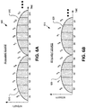
- FIG. 6A a 50 Hz sampling plot 605 of intensity versus time is illustrated. The flickering nature of a light 125 due to its AC power source generates a sine curve 610 in modulated signal 277.
- Modulated signal 277 may be sampled at a rate determined by the clock signal CLK (e.g., 3 MHz).
- each sample block i may include 5000 sample points, depending upon the frequency of the clock signal CLK.
- the coefficients b 0 , b 1 , b 2 , ... b N represent the summation or integration of these sample points within the associated sampling block i, which also represents the area under sine curve 610 within the associated sampling block i.
- the summation sum50 may be accumulated by sum-50 logic 250 for a fixed period of time (e.g., 1 second) or a fixed number clock cycles, and then repeated.
- b i represents an area under a curve per sampling block i of modulated signal 277.
- FIG. 6B a 60 Hz sampling plot 615 of intensity versus time is illustrated. The flickering nature of light 125 due to its AC power source generates a sine curve 620 in modulated signal 277. Again, modulated signal 277 is sampled at a rate determined by the clock signal CLK (e.g., 3 MHz).
- CLK e.g. 3 MHz
- each sample block i may include 5000 sample points, depending upon the frequency of the clock signal CLK.
- the coefficients b 0 , b 1 , b 2 , ... b N represent the summation or integration of these sample points within the associated sampling block i, which also represents the area under sine curve 620 within the associated sampling block i.
- the summation sum60 may be accumulated by sum-60 logic 255 for a fixed period of time (e.g., 1 second) or a fixed number clock cycles, and then repeated. Since sum50 and sum60 are both generated based on modulated signal 277, process blocks 505 and 510 may be performed sequentially in any order, or in parallel.
- comparator logic 260 compares the two summation values to determine which is greater (decision block 515). If comparator logic 260 determines that sum50 is less than sum60, then the power frequency of light 125 is determined to be 50 Hz and comparator logic 260 outputs the frequency select signal indicating such (process block 520). If comparator logic 260 determines that sum50 is greater than sum60, then the power frequency of light 125 is determined to be 60 Hz and comparator logic 260 outputs the frequency select signal indicating such (process block 525).
- the frequency select signal may be provided to pixel control logic 120 to adjust operational parameters of imaging pixel array 115 and improve image acquisition.
- a machine-accessible medium includes any mechanism that provides (i.e., stores) information in a form accessible by a machine (e.g., a computer, network device, personal digital assistant, manufacturing tool, any device with a set of one or more processors, etc.).
- a machine-accessible medium includes recordable/non-recordable media (e.g., read only memory (ROM), random access memory (RAM), magnetic disk storage media, optical storage media, flash memory devices, etc.).
Landscapes
- Engineering & Computer Science (AREA)
- Multimedia (AREA)
- Signal Processing (AREA)
- Optical Modulation, Optical Deflection, Nonlinear Optics, Optical Demodulation, Optical Logic Elements (AREA)
- Transforming Light Signals Into Electric Signals (AREA)
- Photometry And Measurement Of Optical Pulse Characteristics (AREA)
Claims (14)
- Appareil (100) pour déterminer une fréquence industrielle d'une source de lumière (125), l'appareil comprenant :un transistor à jonction bipolaire photosensible, BJT (110), couplé pour générer un signal électrique en réponse à la lumière frappant celui-ci ;un circuit modulateur (205) couplé au transistor BJT pour générer un signal modulé sur la base du signal électrique qui bascule à une fréquence sensiblement proportionnelle à la fréquence industrielle de la source de lumière ; etune unité logique (210) couplée au circuit modulateur pour déterminer une fréquence de basculement du signal modulé et pour générer un signal de sélection de fréquence indiquant la fréquence industrielle de la source de lumière parmi au moins deux fréquences industrielles potentielles différentes,dans lequel le circuit modulateur comprend :un comparateur (230) comprenant des première et deuxième entrées de comparateur et une sortie de comparateur, la première entrée de comparateur étant couplée au transistor BJT et la deuxième entrée de comparateur étant couplée pour recevoir un signal de référence ; etune source de charge (240) configurée pour charger de manière sélective la première entrée de comparateur sur la base d'une rétroaction provenant de la sortie de comparateur ;un commutateur (245) couplé entre la source de charge (240) et un noeud de circuit (N1) qui est couplé au transistor BJT (210) et à la première entrée de comparateur ;une bascule ou une bascule bistable (235) couplée entre la sortie de comparateur et l'unité logique, la bascule ou la bascule bistable comprenant une entrée d'échantillonnage couplée à la sortie de comparateur ; une sortie d'échantillonnage couplée à l'unité logique ; et une entrée d'horloge couplée pour recevoir une entrée d'horloge ;dans lequel une borne de commande du commutateur est couplée à la sortie d'échantillonnage de la bascule ou de la bascule bistable pour commander de manière sélective le couplage de la source de charge (240) au transistor BJT (110) et à la première entrée de comparateur en réponse à la sortie d'échantillonnage ;dans lequel, en réponse au fait que la première entrée de comparateur est inférieure à la deuxième entrée de comparateur, la rétroaction provenant de la sortie de comparateur amène la source de charge à charger la première entrée de comparateur ; etdans lequel, en réponse au fait que la première entrée de comparateur est supérieure à la deuxième entrée de comparateur, la rétroaction provenant de la sortie de comparateur amène la source de charge à arrêter la charge de la première entrée de comparateur.
- Appareil selon la revendication 1, dans lequel le transistor BJT comprend un transistor BJT de type pnp photosensible, dans lequel une borne d'émetteur du transistor BJT de type pnp photosensible est couplée au circuit modulateur et une borne de collecteur du transistor BJT de type pnp photosensible est couplée à un rail de tension.
- Appareil selon la revendication 1, dans lequel le transistor BJT comprend un transistor BJT de type npn photosensible.
- Appareil selon la revendication 1, dans lequel l'unité logique comprend :une première logique de sommation (250) pour générer une première sommation sum50 = ∑Δ|b i+6 - bi |;une deuxième logique de sommation (255) pour générer une deuxième sommation sum60 = ∑Δ|b i+5 - bi |, où bi représente une aire sous une courbe par bloc d'échantillonnage i du signal modulé ; etune logique de comparaison (260) couplée aux première et deuxième logiques de sommation pour déterminer si la première sommation sum50 est supérieure à la deuxième sommation sum60 et couplée pour générer le signal de sélection de fréquence en réponse à la détermination.
- Appareil selon la revendication 1, comprenant en outre une logique de charge couplée pour commander un taux de charge de la source de charge en fonction de l'intensité de la lumière frappant le transistor BJT.
- Appareil selon la revendication 1 comprenant en outre :un réseau de pixels pour capturer une image ;dans lequel au moins une caractéristique de fonctionnement du réseau de pixels peut être ajustée en réponse au signal de sélection de fréquence.
- Appareil selon la revendication 6, comprenant en outre une source d'horloge couplée à l'entrée d'horloge de la bascule ou de la bascule bistable et couplée à l'unité logique, dans lequel le circuit modulateur fonctionne sans commande de rétroaction provenant de l'unité logique.
- Appareil selon la revendication 7, comprenant en outre une logique d'horloge couplée à la source d'horloge pour ajuster une fréquence d'échantillonnage du transistor BJT en ajustant une fréquence d'horloge de la source d'horloge.
- Procédé pour déterminer une fréquence industrielle d'une source de lumière, comprenant :la génération d'un signal électrique en réponse à la lumière émise à partir de la source de lumière et frappant un transistor à jonction bipolaire photosensible, BJT (110) ;la génération d'un signal de modulation sur la base du signal électrique basculant à une fréquence sensiblement proportionnelle à la fréquence industrielle de la source de lumière ; etla détermination de la fréquence de basculement du signal de modulation et la génération d'un signal de sélection de fréquence indiquant la fréquence industrielle de la source de lumière parmi au moins deux fréquences industrielles potentielles différentes,dans lequel la génération du signal de modulation comprend :le couplage du signal électrique provenant du transistor BJT à un noeud de circuit ;la comparaison d'une tension du noeud de circuit à une tension de référence ;le basculement du signal de modulation sur la base de la comparaison ;le verrouillage du signal de modulation synchronisé avec une source d'horloge ; eten réponse à la comparaison, la charge de manière sélective du noeud de circuit (N1) avec une source de charge sur la base de la comparaison en commandant un commutateur couplé entre la source de charge et le noeud de circuit, dans lequel le commutateur est activé/désactivé de manière sélective par une borne de commande du commutateur qui est commutée sur la base du signal de modulation,dans lequel, en réponse à la comparaison indiquant que la tension du noeud de circuit est inférieure à la tension de référence, la charge du noeud de circuit est activée ; etdans lequel, en réponse à la comparaison indiquant que la tension du noeud de circuit est supérieure à la tension de référence, la charge du noeud de circuit est désactivée.
- Procédé selon la revendication 9, dans lequel la détermination de la fréquence industrielle de la lumière comprend :la génération d'une première sommation sum50, dans lequel sum50 = ∑Δ|b i+6 - bi |, où bi représente une aire sous une courbe par bloc d'échantillonnage i du signal modulé ;la génération d'une deuxième sommation sum60, dans lequel sum60 = ∑Δ|b i+5 - bi | ;la comparaison de la première sommation sum50 à la deuxième sommation sum60 ; etla génération d'un signal de sélection de fréquence indiquant la fréquence industrielle sur la base de la comparaison.
- Procédé selon la revendication 9, dans lequel la génération du signal de modulation comprend :le couplage du signal électrique à un noeud de circuit ;la comparaison d'une tension du noeud de circuit à une tension de référence ;le verrouillage du signal de modulation synchronisé avec une source d'horloge ; etla charge ou la décharge de manière sélective du noeud de circuit en réponse au signal de modulation.
- Procédé selon la revendication 11, comprenant en outre l'ajustement d'une plage dynamique de la détermination de la fréquence industrielle en ajustant une fréquence d'horloge de la source d'horloge.
- Procédé selon la revendication 11, comprenant en outre l'ajustement d'une plage de luminance du transistor photosensible en ajustant un taux de la charge ou de la décharge de manière sélective du noeud de circuit.
- Procédé selon la revendication 11, comprenant en outre l'ajustement des paramètres de fonctionnement d'un réseau de pixels pour capturer des images sur la base du signal de sélection de fréquence.
Applications Claiming Priority (2)
| Application Number | Priority Date | Filing Date | Title |
|---|---|---|---|
| US11/942,604 US7847834B2 (en) | 2007-11-19 | 2007-11-19 | Light source frequency detection circuit using bipolar transistor |
| PCT/US2008/082533 WO2009067335A1 (fr) | 2007-11-19 | 2008-11-05 | Circuit de détection de la fréquence d'une source lumineuse à l'aide d'un transistor bipolaire |
Publications (2)
| Publication Number | Publication Date |
|---|---|
| EP2215830A1 EP2215830A1 (fr) | 2010-08-11 |
| EP2215830B1 true EP2215830B1 (fr) | 2018-06-27 |
Family
ID=40263226
Family Applications (1)
| Application Number | Title | Priority Date | Filing Date |
|---|---|---|---|
| EP08853122.3A Active EP2215830B1 (fr) | 2007-11-19 | 2008-11-05 | Circuit de détection de la fréquence d'une source lumineuse à l'aide d'un transistor bipolaire |
Country Status (5)
| Country | Link |
|---|---|
| US (1) | US7847834B2 (fr) |
| EP (1) | EP2215830B1 (fr) |
| CN (1) | CN101868968B (fr) |
| TW (1) | TWI401946B (fr) |
| WO (1) | WO2009067335A1 (fr) |
Families Citing this family (7)
| Publication number | Priority date | Publication date | Assignee | Title |
|---|---|---|---|---|
| NO331527B1 (no) * | 2009-12-23 | 2012-01-23 | Cisco Systems Int Sarl | Metode for a fjerne flimring i videoopptak |
| US8330829B2 (en) | 2009-12-31 | 2012-12-11 | Microsoft Corporation | Photographic flicker detection and compensation |
| CZ2010805A3 (cs) * | 2010-11-08 | 2012-07-11 | Vysoké ucení technické | Zpusob regulace doby spuštení uzáverky fotoaparátu a zarízení pro provádení tohoto zpusobu |
| TWI479888B (zh) * | 2011-05-20 | 2015-04-01 | Microtek Int Inc | 影像感測裝置與影像感測方法 |
| CN105158684A (zh) * | 2015-06-04 | 2015-12-16 | 常熟开关制造有限公司(原常熟开关厂) | 智能断路器故障显示方法、智能断路器、故障识别终端 |
| CN105785121A (zh) * | 2016-03-24 | 2016-07-20 | 航天科技控股集团股份有限公司 | 频率信号采集两种模式复用电路 |
| CN114545214B (zh) * | 2022-02-23 | 2024-10-29 | 上海燧原科技股份有限公司 | 一种电路时钟频率的检查装置及其检查方法 |
Family Cites Families (17)
| Publication number | Priority date | Publication date | Assignee | Title |
|---|---|---|---|---|
| US5053871A (en) | 1989-04-28 | 1991-10-01 | Canon Kabushiki Kaisha | Still video camera with automatic exposure control and flicker detection |
| JPH042282A (ja) | 1990-04-19 | 1992-01-07 | Canon Inc | 撮像装置 |
| US5270553A (en) * | 1992-12-22 | 1993-12-14 | Hewlett-Packard Company | Beginning-of-tape sensor with automatic threshold adjustment |
| JP2002506601A (ja) | 1998-04-27 | 2002-02-26 | コーニンクレッカ フィリップス エレクトロニクス エヌ ヴィ | カメラのフリッカ補正 |
| US6501518B2 (en) * | 1998-07-28 | 2002-12-31 | Intel Corporation | Method and apparatus for reducing flicker effects from discharge lamps during pipelined digital video capture |
| JP3370979B2 (ja) | 2000-09-08 | 2003-01-27 | 三菱電機株式会社 | 撮像装置および自動レベル調整方法 |
| US7187405B2 (en) * | 2001-10-02 | 2007-03-06 | Avago Technologies General Ip (Singapore) Pte. Ltd. | Automatic flicker frequency detection device and method |
| US7288755B1 (en) * | 2001-10-19 | 2007-10-30 | Brian P. Platner | Portable handheld artificial light detector |
| US7009642B2 (en) | 2001-10-30 | 2006-03-07 | Hewlett-Packard Development Company, L.P. | Method and apparatus for detecting the presence of artificial illumination in a scene |
| JP3803924B2 (ja) | 2002-09-09 | 2006-08-02 | 本田技研工業株式会社 | イメージセンサ |
| KR100578647B1 (ko) | 2004-04-27 | 2006-05-11 | 매그나칩 반도체 유한회사 | 이미지센서의 인티그레이션 방법 |
| US20060131484A1 (en) * | 2004-12-17 | 2006-06-22 | Mark Peting | High-dynamic range image sensors |
| KR100715932B1 (ko) | 2005-10-24 | 2007-05-08 | (주) 픽셀플러스 | 플리커 검출장치 |
| US7598987B2 (en) | 2005-11-29 | 2009-10-06 | Stmicroelectronics Asia Pacific Pte. Ltd. | Flicker detection gain control circuit, digital imaging system, and method |
| US8068148B2 (en) * | 2006-01-05 | 2011-11-29 | Qualcomm Incorporated | Automatic flicker correction in an image capture device |
| US7561190B2 (en) | 2006-04-19 | 2009-07-14 | Nethra Imaging Inc. | Method and system to reduce flicker artifacts in captured images |
| US7605359B2 (en) * | 2007-09-14 | 2009-10-20 | Omnivision Technologies, Inc. | Light source frequency detection circuit for image sensor |
-
2007
- 2007-11-19 US US11/942,604 patent/US7847834B2/en active Active
-
2008
- 2008-11-05 EP EP08853122.3A patent/EP2215830B1/fr active Active
- 2008-11-05 CN CN2008801166929A patent/CN101868968B/zh active Active
- 2008-11-05 WO PCT/US2008/082533 patent/WO2009067335A1/fr not_active Ceased
- 2008-11-13 TW TW097143944A patent/TWI401946B/zh active
Non-Patent Citations (1)
| Title |
|---|
| "Halbleiter-Schaltungstechnik", 1 February 1980, SPRINGER VERLAG, ISBN: 978-3-540-09848-5, article ULRICH TIETZE ET AL: "Halbleiterschaltungstechnik", pages: 184-187,410-417, XP055363801 * |
Also Published As
| Publication number | Publication date |
|---|---|
| TWI401946B (zh) | 2013-07-11 |
| US20090128660A1 (en) | 2009-05-21 |
| CN101868968B (zh) | 2013-03-06 |
| US7847834B2 (en) | 2010-12-07 |
| WO2009067335A1 (fr) | 2009-05-28 |
| TW200937948A (en) | 2009-09-01 |
| EP2215830A1 (fr) | 2010-08-11 |
| CN101868968A (zh) | 2010-10-20 |
Similar Documents
| Publication | Publication Date | Title |
|---|---|---|
| US7605359B2 (en) | Light source frequency detection circuit for image sensor | |
| EP2215830B1 (fr) | Circuit de détection de la fréquence d'une source lumineuse à l'aide d'un transistor bipolaire | |
| CN106898675B (zh) | 具有像素级偏置控制的spad阵列 | |
| KR101361788B1 (ko) | 높은 동적 범위 이미지 센서 센서티브 어레이 시스템 및 방법 | |
| US9609243B2 (en) | Systems and methods for providing low-noise readout of an optical sensor | |
| US7807952B2 (en) | Gain calibration in EMCCD cameras | |
| US7218166B2 (en) | Current stabilization circuit, current stabilization method, and solid-state imaging apparatus | |
| US20110267505A1 (en) | Pixel with reduced 1/f noise | |
| TW200405724A (en) | Captured-image-signal processing method and apparatus and imaging apparatus | |
| JP2008539658A (ja) | 照明フリッカ検出 | |
| US20210274114A1 (en) | Image pickup apparatus, solid-state image pickup device, and control method for image pickup apparatus | |
| JP3664035B2 (ja) | 固体撮像装置 | |
| JP4300635B2 (ja) | 固体撮像装置 | |
| Fernández-Peramo et al. | A photovoltaic dynamic vision sensor | |
| US7417678B2 (en) | Precise CMOS imager transfer function control for expanded dynamic range imaging using variable-height multiple reset pulses | |
| US20250126363A1 (en) | Pulse-width modulation pixel sensor | |
| TW200541017A (en) | Method and apparatus for image sensor | |
| JP4320693B2 (ja) | 固体撮像装置 | |
| Konnik et al. | On numerical simulation of high-speed CCD/CMOS-based wavefront sensors in adaptive optics | |
| TWI922015B (zh) | 感測電路及其操作方法 | |
| Deen et al. | CMOS image sensors and camera-on-a-chip for low-light level biomedical applications | |
| JP2014017653A (ja) | 画像情報処理装置 | |
| TW201104240A (en) | Apparatuses and methods for detecting fluorescence |
Legal Events
| Date | Code | Title | Description |
|---|---|---|---|
| PUAI | Public reference made under article 153(3) epc to a published international application that has entered the european phase |
Free format text: ORIGINAL CODE: 0009012 |
|
| 17P | Request for examination filed |
Effective date: 20100616 |
|
| AK | Designated contracting states |
Kind code of ref document: A1 Designated state(s): AT BE BG CH CY CZ DE DK EE ES FI FR GB GR HR HU IE IS IT LI LT LU LV MC MT NL NO PL PT RO SE SI SK TR |
|
| AX | Request for extension of the european patent |
Extension state: AL BA MK RS |
|
| RIN1 | Information on inventor provided before grant (corrected) |
Inventor name: DAI, TIEJUN Inventor name: DENG, LIPING Inventor name: YAO, HONGTAO Inventor name: ZHANG, JINGZHOU Inventor name: MANABE, SOHEI |
|
| DAX | Request for extension of the european patent (deleted) | ||
| 17Q | First examination report despatched |
Effective date: 20140414 |
|
| REG | Reference to a national code |
Ref country code: DE Ref legal event code: R079 Ref document number: 602008055793 Country of ref document: DE Free format text: PREVIOUS MAIN CLASS: H04N0005235000 Ipc: H04N0005140000 |
|
| RIC1 | Information provided on ipc code assigned before grant |
Ipc: H04N 5/14 20060101AFI20171026BHEP |
|
| GRAP | Despatch of communication of intention to grant a patent |
Free format text: ORIGINAL CODE: EPIDOSNIGR1 |
|
| INTG | Intention to grant announced |
Effective date: 20180111 |
|
| GRAS | Grant fee paid |
Free format text: ORIGINAL CODE: EPIDOSNIGR3 |
|
| GRAA | (expected) grant |
Free format text: ORIGINAL CODE: 0009210 |
|
| AK | Designated contracting states |
Kind code of ref document: B1 Designated state(s): AT BE BG CH CY CZ DE DK EE ES FI FR GB GR HR HU IE IS IT LI LT LU LV MC MT NL NO PL PT RO SE SI SK TR |
|
| REG | Reference to a national code |
Ref country code: GB Ref legal event code: FG4D |
|
| REG | Reference to a national code |
Ref country code: AT Ref legal event code: REF Ref document number: 1013339 Country of ref document: AT Kind code of ref document: T Effective date: 20180715 |
|
| REG | Reference to a national code |
Ref country code: IE Ref legal event code: FG4D |
|
| REG | Reference to a national code |
Ref country code: DE Ref legal event code: R096 Ref document number: 602008055793 Country of ref document: DE |
|
| REG | Reference to a national code |
Ref country code: FR Ref legal event code: PLFP Year of fee payment: 11 |
|
| PG25 | Lapsed in a contracting state [announced via postgrant information from national office to epo] |
Ref country code: NO Free format text: LAPSE BECAUSE OF FAILURE TO SUBMIT A TRANSLATION OF THE DESCRIPTION OR TO PAY THE FEE WITHIN THE PRESCRIBED TIME-LIMIT Effective date: 20180927 Ref country code: FI Free format text: LAPSE BECAUSE OF FAILURE TO SUBMIT A TRANSLATION OF THE DESCRIPTION OR TO PAY THE FEE WITHIN THE PRESCRIBED TIME-LIMIT Effective date: 20180627 Ref country code: BG Free format text: LAPSE BECAUSE OF FAILURE TO SUBMIT A TRANSLATION OF THE DESCRIPTION OR TO PAY THE FEE WITHIN THE PRESCRIBED TIME-LIMIT Effective date: 20180927 Ref country code: SE Free format text: LAPSE BECAUSE OF FAILURE TO SUBMIT A TRANSLATION OF THE DESCRIPTION OR TO PAY THE FEE WITHIN THE PRESCRIBED TIME-LIMIT Effective date: 20180627 Ref country code: LT Free format text: LAPSE BECAUSE OF FAILURE TO SUBMIT A TRANSLATION OF THE DESCRIPTION OR TO PAY THE FEE WITHIN THE PRESCRIBED TIME-LIMIT Effective date: 20180627 |
|
| REG | Reference to a national code |
Ref country code: NL Ref legal event code: MP Effective date: 20180627 |
|
| REG | Reference to a national code |
Ref country code: LT Ref legal event code: MG4D |
|
| PG25 | Lapsed in a contracting state [announced via postgrant information from national office to epo] |
Ref country code: LV Free format text: LAPSE BECAUSE OF FAILURE TO SUBMIT A TRANSLATION OF THE DESCRIPTION OR TO PAY THE FEE WITHIN THE PRESCRIBED TIME-LIMIT Effective date: 20180627 Ref country code: GR Free format text: LAPSE BECAUSE OF FAILURE TO SUBMIT A TRANSLATION OF THE DESCRIPTION OR TO PAY THE FEE WITHIN THE PRESCRIBED TIME-LIMIT Effective date: 20180928 Ref country code: HR Free format text: LAPSE BECAUSE OF FAILURE TO SUBMIT A TRANSLATION OF THE DESCRIPTION OR TO PAY THE FEE WITHIN THE PRESCRIBED TIME-LIMIT Effective date: 20180627 |
|
| REG | Reference to a national code |
Ref country code: AT Ref legal event code: MK05 Ref document number: 1013339 Country of ref document: AT Kind code of ref document: T Effective date: 20180627 |
|
| PG25 | Lapsed in a contracting state [announced via postgrant information from national office to epo] |
Ref country code: NL Free format text: LAPSE BECAUSE OF FAILURE TO SUBMIT A TRANSLATION OF THE DESCRIPTION OR TO PAY THE FEE WITHIN THE PRESCRIBED TIME-LIMIT Effective date: 20180627 |
|
| PG25 | Lapsed in a contracting state [announced via postgrant information from national office to epo] |
Ref country code: IS Free format text: LAPSE BECAUSE OF FAILURE TO SUBMIT A TRANSLATION OF THE DESCRIPTION OR TO PAY THE FEE WITHIN THE PRESCRIBED TIME-LIMIT Effective date: 20181027 Ref country code: EE Free format text: LAPSE BECAUSE OF FAILURE TO SUBMIT A TRANSLATION OF THE DESCRIPTION OR TO PAY THE FEE WITHIN THE PRESCRIBED TIME-LIMIT Effective date: 20180627 Ref country code: AT Free format text: LAPSE BECAUSE OF FAILURE TO SUBMIT A TRANSLATION OF THE DESCRIPTION OR TO PAY THE FEE WITHIN THE PRESCRIBED TIME-LIMIT Effective date: 20180627 Ref country code: RO Free format text: LAPSE BECAUSE OF FAILURE TO SUBMIT A TRANSLATION OF THE DESCRIPTION OR TO PAY THE FEE WITHIN THE PRESCRIBED TIME-LIMIT Effective date: 20180627 Ref country code: CZ Free format text: LAPSE BECAUSE OF FAILURE TO SUBMIT A TRANSLATION OF THE DESCRIPTION OR TO PAY THE FEE WITHIN THE PRESCRIBED TIME-LIMIT Effective date: 20180627 Ref country code: SK Free format text: LAPSE BECAUSE OF FAILURE TO SUBMIT A TRANSLATION OF THE DESCRIPTION OR TO PAY THE FEE WITHIN THE PRESCRIBED TIME-LIMIT Effective date: 20180627 Ref country code: PL Free format text: LAPSE BECAUSE OF FAILURE TO SUBMIT A TRANSLATION OF THE DESCRIPTION OR TO PAY THE FEE WITHIN THE PRESCRIBED TIME-LIMIT Effective date: 20180627 |
|
| PG25 | Lapsed in a contracting state [announced via postgrant information from national office to epo] |
Ref country code: IT Free format text: LAPSE BECAUSE OF FAILURE TO SUBMIT A TRANSLATION OF THE DESCRIPTION OR TO PAY THE FEE WITHIN THE PRESCRIBED TIME-LIMIT Effective date: 20180627 Ref country code: ES Free format text: LAPSE BECAUSE OF FAILURE TO SUBMIT A TRANSLATION OF THE DESCRIPTION OR TO PAY THE FEE WITHIN THE PRESCRIBED TIME-LIMIT Effective date: 20180627 |
|
| REG | Reference to a national code |
Ref country code: DE Ref legal event code: R097 Ref document number: 602008055793 Country of ref document: DE |
|
| PLBE | No opposition filed within time limit |
Free format text: ORIGINAL CODE: 0009261 |
|
| STAA | Information on the status of an ep patent application or granted ep patent |
Free format text: STATUS: NO OPPOSITION FILED WITHIN TIME LIMIT |
|
| PG25 | Lapsed in a contracting state [announced via postgrant information from national office to epo] |
Ref country code: DK Free format text: LAPSE BECAUSE OF FAILURE TO SUBMIT A TRANSLATION OF THE DESCRIPTION OR TO PAY THE FEE WITHIN THE PRESCRIBED TIME-LIMIT Effective date: 20180627 |
|
| 26N | No opposition filed |
Effective date: 20190328 |
|
| PG25 | Lapsed in a contracting state [announced via postgrant information from national office to epo] |
Ref country code: LU Free format text: LAPSE BECAUSE OF NON-PAYMENT OF DUE FEES Effective date: 20181105 Ref country code: MC Free format text: LAPSE BECAUSE OF FAILURE TO SUBMIT A TRANSLATION OF THE DESCRIPTION OR TO PAY THE FEE WITHIN THE PRESCRIBED TIME-LIMIT Effective date: 20180627 |
|
| REG | Reference to a national code |
Ref country code: BE Ref legal event code: MM Effective date: 20181130 |
|
| REG | Reference to a national code |
Ref country code: IE Ref legal event code: MM4A |
|
| PG25 | Lapsed in a contracting state [announced via postgrant information from national office to epo] |
Ref country code: SI Free format text: LAPSE BECAUSE OF FAILURE TO SUBMIT A TRANSLATION OF THE DESCRIPTION OR TO PAY THE FEE WITHIN THE PRESCRIBED TIME-LIMIT Effective date: 20180627 |
|
| PG25 | Lapsed in a contracting state [announced via postgrant information from national office to epo] |
Ref country code: IE Free format text: LAPSE BECAUSE OF NON-PAYMENT OF DUE FEES Effective date: 20181105 |
|
| PG25 | Lapsed in a contracting state [announced via postgrant information from national office to epo] |
Ref country code: BE Free format text: LAPSE BECAUSE OF NON-PAYMENT OF DUE FEES Effective date: 20181130 |
|
| PG25 | Lapsed in a contracting state [announced via postgrant information from national office to epo] |
Ref country code: MT Free format text: LAPSE BECAUSE OF NON-PAYMENT OF DUE FEES Effective date: 20181105 |
|
| PG25 | Lapsed in a contracting state [announced via postgrant information from national office to epo] |
Ref country code: TR Free format text: LAPSE BECAUSE OF FAILURE TO SUBMIT A TRANSLATION OF THE DESCRIPTION OR TO PAY THE FEE WITHIN THE PRESCRIBED TIME-LIMIT Effective date: 20180627 |
|
| PG25 | Lapsed in a contracting state [announced via postgrant information from national office to epo] |
Ref country code: PT Free format text: LAPSE BECAUSE OF FAILURE TO SUBMIT A TRANSLATION OF THE DESCRIPTION OR TO PAY THE FEE WITHIN THE PRESCRIBED TIME-LIMIT Effective date: 20180627 |
|
| PG25 | Lapsed in a contracting state [announced via postgrant information from national office to epo] |
Ref country code: HU Free format text: LAPSE BECAUSE OF FAILURE TO SUBMIT A TRANSLATION OF THE DESCRIPTION OR TO PAY THE FEE WITHIN THE PRESCRIBED TIME-LIMIT; INVALID AB INITIO Effective date: 20081105 Ref country code: CY Free format text: LAPSE BECAUSE OF FAILURE TO SUBMIT A TRANSLATION OF THE DESCRIPTION OR TO PAY THE FEE WITHIN THE PRESCRIBED TIME-LIMIT Effective date: 20180627 |
|
| P01 | Opt-out of the competence of the unified patent court (upc) registered |
Effective date: 20230418 |
|
| REG | Reference to a national code |
Ref country code: CH Ref legal event code: U11 Free format text: ST27 STATUS EVENT CODE: U-0-0-U10-U11 (AS PROVIDED BY THE NATIONAL OFFICE) Effective date: 20251201 |
|
| PGFP | Annual fee paid to national office [announced via postgrant information from national office to epo] |
Ref country code: DE Payment date: 20251013 Year of fee payment: 18 |
|
| PGFP | Annual fee paid to national office [announced via postgrant information from national office to epo] |
Ref country code: GB Payment date: 20251009 Year of fee payment: 18 |
|
| PGFP | Annual fee paid to national office [announced via postgrant information from national office to epo] |
Ref country code: FR Payment date: 20251013 Year of fee payment: 18 |
|
| PGFP | Annual fee paid to national office [announced via postgrant information from national office to epo] |
Ref country code: CH Payment date: 20251201 Year of fee payment: 18 |