EP2205052A1 - Circuit connecting method - Google Patents
Circuit connecting method Download PDFInfo
- Publication number
- EP2205052A1 EP2205052A1 EP08710856A EP08710856A EP2205052A1 EP 2205052 A1 EP2205052 A1 EP 2205052A1 EP 08710856 A EP08710856 A EP 08710856A EP 08710856 A EP08710856 A EP 08710856A EP 2205052 A1 EP2205052 A1 EP 2205052A1
- Authority
- EP
- European Patent Office
- Prior art keywords
- circuit
- conductive film
- anisotropic conductive
- electrodes
- connection
- Prior art date
- Legal status (The legal status is an assumption and is not a legal conclusion. Google has not performed a legal analysis and makes no representation as to the accuracy of the status listed.)
- Withdrawn
Links
Images


Classifications
-
- H—ELECTRICITY
- H05—ELECTRIC TECHNIQUES NOT OTHERWISE PROVIDED FOR
- H05K—PRINTED CIRCUITS; CASINGS OR CONSTRUCTIONAL DETAILS OF ELECTRIC APPARATUS; MANUFACTURE OF ASSEMBLAGES OF ELECTRICAL COMPONENTS
- H05K1/00—Printed circuits
- H05K1/02—Details
- H05K1/14—Structural association of two or more printed circuits
-
- H—ELECTRICITY
- H05—ELECTRIC TECHNIQUES NOT OTHERWISE PROVIDED FOR
- H05K—PRINTED CIRCUITS; CASINGS OR CONSTRUCTIONAL DETAILS OF ELECTRIC APPARATUS; MANUFACTURE OF ASSEMBLAGES OF ELECTRICAL COMPONENTS
- H05K3/00—Apparatus or processes for manufacturing printed circuits
- H05K3/36—Assembling printed circuits with other printed circuits
- H05K3/361—Assembling flexible printed circuits with other printed circuits
-
- C—CHEMISTRY; METALLURGY
- C08—ORGANIC MACROMOLECULAR COMPOUNDS; THEIR PREPARATION OR CHEMICAL WORKING-UP; COMPOSITIONS BASED THEREON
- C08J—WORKING-UP; GENERAL PROCESSES OF COMPOUNDING; AFTER-TREATMENT NOT COVERED BY SUBCLASSES C08B, C08C, C08F, C08G or C08H
- C08J5/00—Manufacture of articles or shaped materials containing macromolecular substances
- C08J5/18—Manufacture of films or sheets
-
- G—PHYSICS
- G02—OPTICS
- G02F—OPTICAL DEVICES OR ARRANGEMENTS FOR THE CONTROL OF LIGHT BY MODIFICATION OF THE OPTICAL PROPERTIES OF THE MEDIA OF THE ELEMENTS INVOLVED THEREIN; NON-LINEAR OPTICS; FREQUENCY-CHANGING OF LIGHT; OPTICAL LOGIC ELEMENTS; OPTICAL ANALOGUE/DIGITAL CONVERTERS
- G02F1/00—Devices or arrangements for the control of the intensity, colour, phase, polarisation or direction of light arriving from an independent light source, e.g. switching, gating or modulating; Non-linear optics
- G02F1/01—Devices or arrangements for the control of the intensity, colour, phase, polarisation or direction of light arriving from an independent light source, e.g. switching, gating or modulating; Non-linear optics for the control of the intensity, phase, polarisation or colour
- G02F1/13—Devices or arrangements for the control of the intensity, colour, phase, polarisation or direction of light arriving from an independent light source, e.g. switching, gating or modulating; Non-linear optics for the control of the intensity, phase, polarisation or colour based on liquid crystals, e.g. single liquid crystal display cells
-
- H—ELECTRICITY
- H05—ELECTRIC TECHNIQUES NOT OTHERWISE PROVIDED FOR
- H05K—PRINTED CIRCUITS; CASINGS OR CONSTRUCTIONAL DETAILS OF ELECTRIC APPARATUS; MANUFACTURE OF ASSEMBLAGES OF ELECTRICAL COMPONENTS
- H05K2201/00—Indexing scheme relating to printed circuits covered by H05K1/00
- H05K2201/01—Dielectrics
- H05K2201/0183—Dielectric layers
- H05K2201/0191—Dielectric layers wherein the thickness of the dielectric plays an important role
-
- H—ELECTRICITY
- H05—ELECTRIC TECHNIQUES NOT OTHERWISE PROVIDED FOR
- H05K—PRINTED CIRCUITS; CASINGS OR CONSTRUCTIONAL DETAILS OF ELECTRIC APPARATUS; MANUFACTURE OF ASSEMBLAGES OF ELECTRICAL COMPONENTS
- H05K2203/00—Indexing scheme relating to apparatus or processes for manufacturing printed circuits covered by H05K3/00
- H05K2203/05—Patterning and lithography; Masks; Details of resist
- H05K2203/0562—Details of resist
- H05K2203/0594—Insulating resist or coating with special shaped edges
-
- H—ELECTRICITY
- H05—ELECTRIC TECHNIQUES NOT OTHERWISE PROVIDED FOR
- H05K—PRINTED CIRCUITS; CASINGS OR CONSTRUCTIONAL DETAILS OF ELECTRIC APPARATUS; MANUFACTURE OF ASSEMBLAGES OF ELECTRICAL COMPONENTS
- H05K3/00—Apparatus or processes for manufacturing printed circuits
- H05K3/22—Secondary treatment of printed circuits
- H05K3/28—Applying non-metallic protective coatings
-
- H—ELECTRICITY
- H05—ELECTRIC TECHNIQUES NOT OTHERWISE PROVIDED FOR
- H05K—PRINTED CIRCUITS; CASINGS OR CONSTRUCTIONAL DETAILS OF ELECTRIC APPARATUS; MANUFACTURE OF ASSEMBLAGES OF ELECTRICAL COMPONENTS
- H05K3/00—Apparatus or processes for manufacturing printed circuits
- H05K3/30—Assembling printed circuits with electric components, e.g. with resistors
- H05K3/32—Assembling printed circuits with electric components, e.g. with resistors electrically connecting electric components or wires to printed circuits
- H05K3/321—Assembling printed circuits with electric components, e.g. with resistors electrically connecting electric components or wires to printed circuits by conductive adhesives
- H05K3/323—Assembling printed circuits with electric components, e.g. with resistors electrically connecting electric components or wires to printed circuits by conductive adhesives by applying an anisotropic conductive adhesive layer over an array of pads
-
- Y—GENERAL TAGGING OF NEW TECHNOLOGICAL DEVELOPMENTS; GENERAL TAGGING OF CROSS-SECTIONAL TECHNOLOGIES SPANNING OVER SEVERAL SECTIONS OF THE IPC; TECHNICAL SUBJECTS COVERED BY FORMER USPC CROSS-REFERENCE ART COLLECTIONS [XRACs] AND DIGESTS
- Y10—TECHNICAL SUBJECTS COVERED BY FORMER USPC
- Y10T—TECHNICAL SUBJECTS COVERED BY FORMER US CLASSIFICATION
- Y10T29/00—Metal working
- Y10T29/49—Method of mechanical manufacture
- Y10T29/49002—Electrical device making
- Y10T29/49117—Conductor or circuit manufacturing
- Y10T29/49124—On flat or curved insulated base, e.g., printed circuit, etc.
- Y10T29/49126—Assembling bases
-
- Y—GENERAL TAGGING OF NEW TECHNOLOGICAL DEVELOPMENTS; GENERAL TAGGING OF CROSS-SECTIONAL TECHNOLOGIES SPANNING OVER SEVERAL SECTIONS OF THE IPC; TECHNICAL SUBJECTS COVERED BY FORMER USPC CROSS-REFERENCE ART COLLECTIONS [XRACs] AND DIGESTS
- Y10—TECHNICAL SUBJECTS COVERED BY FORMER USPC
- Y10T—TECHNICAL SUBJECTS COVERED BY FORMER US CLASSIFICATION
- Y10T29/00—Metal working
- Y10T29/49—Method of mechanical manufacture
- Y10T29/49002—Electrical device making
- Y10T29/49117—Conductor or circuit manufacturing
- Y10T29/49124—On flat or curved insulated base, e.g., printed circuit, etc.
- Y10T29/4913—Assembling to base an electrical component, e.g., capacitor, etc.
-
- Y—GENERAL TAGGING OF NEW TECHNOLOGICAL DEVELOPMENTS; GENERAL TAGGING OF CROSS-SECTIONAL TECHNOLOGIES SPANNING OVER SEVERAL SECTIONS OF THE IPC; TECHNICAL SUBJECTS COVERED BY FORMER USPC CROSS-REFERENCE ART COLLECTIONS [XRACs] AND DIGESTS
- Y10—TECHNICAL SUBJECTS COVERED BY FORMER USPC
- Y10T—TECHNICAL SUBJECTS COVERED BY FORMER US CLASSIFICATION
- Y10T29/00—Metal working
- Y10T29/49—Method of mechanical manufacture
- Y10T29/49002—Electrical device making
- Y10T29/49117—Conductor or circuit manufacturing
- Y10T29/49124—On flat or curved insulated base, e.g., printed circuit, etc.
- Y10T29/4913—Assembling to base an electrical component, e.g., capacitor, etc.
- Y10T29/49144—Assembling to base an electrical component, e.g., capacitor, etc. by metal fusion
Definitions
- the present invention relates to a circuit connecting method.
- circuit-bonding methods for such circuits have been desired that have reliability equivalent or superior to conventional reliability.
- Circuit-bonding methods have therefore been developed wherein, on a flexible board with circuit bonded sections that are bonded using an anisotropic conductive film for circuit connection, a circuit-protecting member (solder resist) is provided at the sections of circuit electrodes outside of the circuit-bonded sections to protect those sections, and during circuit bonding between circuit electrodes on the flexible board and circuit electrodes on a glass substrate with an anisotropic conductive film for circuit connection, the anisotropic conductive film for circuit connection is also attached to a part of the circuit-protecting member in addition to the circuit-bonded sections (see Patent document 1, for example).
- a circuit-protecting member solder resist
- the circuit electrodes on the flexible board are protected by the circuit-protecting member and anisotropic conductive film for circuit connection, thus helping to prevent wire breakage of the circuit electrodes on the flexible board and producing high bonding strength between the circuit electrodes.
- the circuit-protecting member and anisotropic conductive film for circuit connection overlap during circuit bonding between the circuit electrodes on the flexible board and the circuit electrodes on the glass substrate with an anisotropic conductive film for circuit connection, and therefore the anisotropic conductive film for circuit connection present near the circuit-protecting member is not easily eliminated between the circuit electrodes that are adjacent to each other, and the connection resistance between the circuit electrodes that are electrically connected by the anisotropic conductive film for circuit connection is increased.
- the circuit connecting method of the invention comprises a step of preparing a first circuit member having first circuit electrodes formed on the main surface of a first board, a step of preparing a second circuit member having second circuit electrodes formed on the main surface of a second board, with an insulating layer provided on the sections of the second circuit electrodes other that the sections that are connected to the first circuit electrodes and a step of bonding the first circuit member and second circuit member via an anisotropic conductive film for circuit connection so that part of the anisotropic conductive film for circuit connection overlaps part of the insulating layer, for electrical connection between the first circuit electrodes and second circuit electrodes, wherein the thickness of the anisotropic conductive film for circuit connection is no greater than the total of the height of the first circuit electrodes and the height of the second circuit electrodes.
- the first circuit member and second circuit member are bonded via the anisotropic conductive film for circuit connection, and the thickness of the anisotropic conductive film for circuit connection is no greater than the total of the height of the first circuit electrodes and the height of the second circuit electrodes.
- the part of the anisotropic conductive film for circuit connection between the first circuit electrodes and second circuit electrodes remain between the first circuit electrodes and second circuit electrodes only in the amount required to electrically connect and bond the first circuit electrodes and second circuit electrodes, while the rest is eliminated between the adjacent electrodes among the first circuit electrodes and the adjacent electrodes among the second circuit electrodes.
- the anisotropic conductive film for circuit connection is greater than the total of the height of the first circuit electrodes and the height of the second circuit electrodes, the part of the anisotropic conductive film for circuit connection between the first circuit electrodes and second circuit electrodes will not be easily eliminated between the adjacent electrodes among the first circuit electrodes and the adjacent electrodes among the second circuit electrodes.
- the thickness of the anisotropic conductive film for circuit connection is no greater than 70% of the total of the height of the first circuit electrodes and the height of the second circuit electrodes. This will further promote elimination of the part of the anisotropic conductive film for circuit connection between the first circuit electrodes and second circuit electrodes, for between the adjacent electrodes among the first circuit electrodes and the adjacent electrodes among the second circuit electrodes.
- the thickness of the anisotropic conductive film for circuit connection is at least 50% of the total of the height of the first circuit electrodes and the height of the second circuit electrodes. If the thickness of the anisotropic conductive film for circuit connection is less than 50% of the total of the height of the first circuit electrodes and the height of the second circuit electrodes, the anisotropic conductive film for circuit connection will not sufficiently fill between the adjacent electrodes among the first circuit electrodes and the adjacent electrodes among the second circuit electrodes, thus lowering the bonding strength between the first circuit member and second circuit member while also tending to reduce the electrical insulating property between the adjacent electrodes among the first circuit electrodes and the electrical insulating property between the adjacent electrodes among the second circuit electrodes.
- At least one of the first circuit member and second circuit member is flexible wiring boards.
- the first board material is glass and the second circuit member is a flexible wiring board.
- circuit connecting method that can sufficiently reduce connection resistance between circuit electrodes that are electrically connected via an anisotropic conductive film for circuit connection, even when a part of the circuit-protecting member is bonded with the anisotropic conductive film for circuit connection in addition to the circuit-bonded sections of the circuit electrodes.
- 10 Liquid crystal display device
- 12 circuit member (first circuit member)
- 12a first board
- 12b first circuit electrode
- 14 flexible wiring board (second circuit member)
- 14a second board
- 14b second circuit electrode
- 16 anisotropic conductive film for circuit connection
- 18 solder resist (insulating layer).
- the construction of a liquid crystal display device 10 in which the circuit connecting method of the invention was applied will be explained first, with reference to Fig. 1 and Fig. 2 .
- the liquid crystal display device 10 comprises a circuit member (first circuit member) 12, a flexible wiring board (second circuit member) 14, and an anisotropic conductive film for circuit connection 16.
- the circuit member 12 comprises a glass substrate (first board) 12a and circuit electrodes (first circuit electrodes) 12b.
- the glass substrate 12a together with another glass substrate (not shown), sandwiches the liquid crystal layer to form a liquid crystal panel.
- the circuit electrodes 12b are a transparent electrode made of ITO (indium tin oxide), for example, and they are formed on the main surface of the glass substrate 12a.
- the circuit electrodes 12b have the function of applying a voltage to the liquid crystals in the liquid crystal layer to drive the liquid crystals.
- the height h1 of the circuit electrodes 12b may be about 0.05 ⁇ m-0.7 ⁇ m, for example.
- the flexible wiring board 14 comprises a base (second board) 14a and circuit electrodes (second circuit electrodes) 14b.
- the base 14a may be a polyimide film, for example.
- the circuit electrodes 14b are composed of Cu with a Sn plating, for example, and they are formed on the main surface of the base 14a.
- solder resist (insulating layer) 18 As a protecting member to protect the circuit electrodes 14b.
- the height h2 of the circuit electrodes 14b may be about 5 ⁇ m-100 ⁇ m, for example.
- the anisotropic conductive film for circuit connection 16 has conductive particles 16b evenly dispersed in a thermosetting adhesive 16a.
- the anisotropic conductive film for circuit connection 16 has anisotropic conductivity such that it exhibits conductivity in the thickness direction in which force is applied, but exhibits no conductivity in the in-plane direction.
- the anisotropic conductive film for circuit connection 16 may be any adhesive film containing conductive particles 16b, without any particular restrictions, and using the thermosetting adhesive 16a as mentioned above results in a more notable effect of the invention with higher temperature and shorter time for the circuit connection conditions.
- the anisotropic conductive film for circuit connection 16 bonds the circuit member 12 and flexible wiring board 14. Specifically, the anisotropic conductive film for circuit connection 16 is disposed between the circuit member 12 and part of the flexible wiring board 14 connected to the circuit member 12 and part of the solder resist 18, with a part of the anisotropic conductive film for circuit connection 16 overlapping a part of the solder resist 18.
- the section of the anisotropic conductive film for circuit connection 16 other than the section that is between the circuit electrodes 12b and circuit electrodes 14b fills the area between the adjacent electrodes among each of the circuit electrodes 12b and the adjacent electrodes among each of the circuit electrodes 14b, so that the circuit electrodes 12b and circuit electrodes 14b become electrically connected by the conductive particles 16b.
- a circuit member 12 liquid crystal panel having a circuit electrode 12b formed on the main surface of a glass substrate 12a is prepared.
- a flexible wiring board 14 is also prepared having circuit electrodes 14b formed on the main surface of a base 14a and having a solder resist 18 provided on the sections of the circuit electrodes 14b other than the section that are connected to the circuit electrodes 12b.
- An anisotropic conductive film for circuit connection 16 is also prepared.
- the anisotropic conductive film for circuit connection 16 has a thickness h3 before connection of the circuit member 12 and flexible wiring board 14, which is no greater than the total of the height h1 of the circuit electrodes 12b and the height h2 of the circuit electrodes 14b, and it may be 5.05 ⁇ m-100.7 ⁇ m, for example.
- the thickness h3 of the anisotropic conductive film for circuit connection 16 is preferably no greater than 70% of the total of the height h1 of the circuit electrodes 12b and the height h2 of the circuit electrodes 14b. This will further promote elimination of the part of the anisotropic conductive film for circuit connection 16 between the first circuit electrodes 12b and second circuit electrodes 14b, for between the adjacent electrodes among each of the first circuit electrodes 12b and the adjacent electrodes among each of the second circuit electrodes 14b.
- the thickness h3 of the anisotropic conductive film for circuit connection 16 is preferably at least 50% of the total of the height h1 of the circuit electrodes 12b and the height h2 of the circuit electrodes 14b. If the thickness h3 of the anisotropic conductive film for circuit connection 16 is less than 50% of the total of the height h1 of the first circuit electrodes 12b and the height h2 of the second circuit electrodes 14b, the anisotropic conductive film for circuit connection 16 will not sufficiently fill between the adjacent electrodes among each of the first circuit electrodes 12b and the adjacent electrodes among each of the second circuit electrodes 14b, thus lowering the bonding strength between the first circuit member 12b and second circuit member 14b while also tending to reduce the electrical insulating property between the adjacent electrodes among each of the first circuit electrodes 12b and the electrical insulating property between the adjacent electrodes among each of the second circuit electrodes 14b.
- the anisotropic conductive film for circuit connection 16 is disposed between the circuit member 12 and flexible wiring board 14, and the anisotropic conductive film for circuit connection 16 is sandwiched by the circuit member 12 and flexible wiring board 14 so that part of the anisotropic conductive film for circuit connection 16 overlaps with part of the solder resist 18.
- the circuit member 12 and flexible wiring board 14 are bonded via the anisotropic conductive film for circuit connection 16 in this manner to complete the liquid crystal display device.
- the circuit member 12 and flexible wiring board 14 are bonded via the anisotropic conductive film for circuit connection 16, and the thickness h3 of the anisotropic conductive film for circuit connection 16 is no greater than the total of the height h1 of the circuit electrodes 12b and the height h2 of the circuit electrodes 14b.
- the part of the anisotropic conductive film for circuit connection 16 between the circuit electrodes 12b and circuit electrodes 14b remain between the circuit electrodes 12b and circuit electrodes 14b only in the amount required to electrically connect and bond the circuit electrodes 12b and circuit electrodes 14b, while the rest is eliminated between the adjacent electrodes among each of the circuit electrodes 12b and the adjacent electrodes among each of the circuit electrodes 14b.
- the above detailed explanation of a preferred embodiment of the invention is not intended to restrict the scope of the invention to this particular embodiment.
- the invention can also be applied to display devices other than liquid crystal display devices (such as plasma displays or organic EL displays).
- circuit member 12 glass substrate 12a
- flexible wiring board 14 are bonded by the anisotropic conductive film for circuit connection 16 in this embodiment
- two glass substrates may be bonded instead, or two flexible wiring boards may be bonded instead.
- Different circuit members other than these may also be bonded together.
- the line widths of the circuit electrodes 12b were 25 ⁇ m and the pitch was 50 ⁇ m.
- the line widths of the circuit electrodes 14b were 18 ⁇ m and the pitch was 50 ⁇ m.
- a solder resist 18 (“SN-9000” solder resist by Hitachi Chemical Co., Ltd.) was provided as a protecting member to protect the circuit electrodes 14b, on the sections of the circuit electrodes 14b other than the sections that are connected to the circuit electrodes 12b.
- the thickness of the solder resist 18 was 30 ⁇ m and the width was 10 mm.
- the circuit member 12 and flexible wiring board 14 were positioned at a circuit bonding width of 1.5 mm and the anisotropic conductive film for circuit connection 16 was sandwiched by the circuit member 12 and flexible wiring board 14 and hot pressed at 180°C, 3 MPa for 15 seconds to obtain a liquid crystal display device 10 for Example 1-1.
- the anisotropic conductive film for circuit connection 16 and solder resist 18 had an overlap of 0.5 mm.
- a liquid crystal display device 10 for Example 1-2 was obtained in the same manner as Example 1-1, except that the anisotropic conductive film for circuit connection 16 was sandwiched by the circuit member 12 and flexible wiring board 14 and hot pressed at 210°C, 3 MPa for 15 seconds.
- a liquid crystal display device 10 for Example 2-1 was obtained in the same manner as Example 1-1, except that the anisotropic conducive film for circuit connection 16 had a thickness h3 of 6 ⁇ m ("ANISOLM: AC-7206U-6" anisotropic conductive film by Hitachi Chemical Co., Ltd.).
- a liquid crystal display device 10 for Example 2-2 was obtained in the same manner as Example 1-1, except that the anisotropic conductive film for circuit connection 16 had a thickness h3 of 6 ⁇ m ("ANISOLM: AC-7206U-6" anisotropic conductive film by Hitachi Chemical Co., Ltd.), and the anisotropic conductive film for circuit connection 16 was sandwiched by the circuit member 12 and flexible wiring board 14 and hot pressed at 210°C, 3 MPa for 15 seconds.
- a liquid crystal display device 10 for Example 3-1 was obtained in the same manner as Example 1-1, except that the anisotropic conductive film for circuit connection 16 had a thickness h3 of 8 ⁇ m ("ANISOLM: AC-11000Y-8" anisotropic conductive film by Hitachi Chemical Co., Ltd.), and the anisotropic conductive film for circuit connection 16 was sandwiched by the circuit member 12 and flexible wiring board 14 and hot pressed at 180°C, 3 MPa for 5 seconds.
- a liquid crystal display device 10 for Example 3-2 was obtained in the same manner as Example 1-1, except that the anisotropic conductive film for circuit connection 16 had a thickness h3 of 8 ⁇ m ("ANISOLM: AC-11000Y-8" anisotropic conductive film by Hitachi Chemical Co., Ltd.), and the anisotropic conductive film for circuit connection 16 was sandwiched by the circuit member 12 and flexible wiring board 14 and hot pressed at 210°C, 3 MPa for 5 seconds.
- ANISOLM: AC-11000Y-8 anisotropic conductive film by Hitachi Chemical Co., Ltd.
- a liquid crystal display device 10 for Example 4-1 was obtained in the same manner as Example 1-1, except that the anisotropic conductive film for circuit connection 16 had a thickness h3 of 6 ⁇ m ("ANISOLM: AC-11000Y-6" anisotropic conductive film by Hitachi Chemical Co., Ltd.), and the anisotropic conductive film for circuit connection 16 was sandwiched by the circuit member 12 and flexible wiring board 14 and hot pressed at 180°C, 3 MPa for 5 seconds.
- a liquid crystal display device 10 for Example 4-2 was obtained in the same manner as Example 1-1, except that the anisotropic conductive film for circuit connection 16 had a thickness h3 of 6 ⁇ m ("ANISOLM: AC-11000Y-6" anisotropic conductive film by Hitachi Chemical Co., Ltd.), and the anisotropic conductive film for circuit connection 16 was sandwiched by the circuit member 12 and flexible wiring board 14 and hot pressed at 210°C, 3 MPa for 5 seconds.
- the line widths of the circuit electrodes 12b were 25 ⁇ m and the pitch was 50 ⁇ m.
- the line widths of the circuit electrodes 14b were 18 ⁇ m and the pitch was 50 ⁇ m.
- a solder resist 18 (“SN-9000” solder resist by Hitachi Chemical Co., Ltd.) was provided as a protecting member to protect the circuit electrodes 14b, on the sections of the circuit electrodes 14b other than the sections that are connected to the circuit electrodes 12b.
- the thickness of the solder resist 18 was 30 ⁇ m and the width was 10 mm.
- anisotropic conductive film for circuit connection 16 with a thickness h3 of 12 ⁇ m ("ANISOLM: AC-7206U-12" anisotropic conductive film by Hitachi Chemical Co., Ltd.).
- the circuit member 12 and flexible wiring board 14 were positioned at a circuit bonding width of 1.5 mm and the anisotropic conductive film for circuit connection 16 was sandwiched by the circuit member 12 and flexible wiring board 14 and hot pressed at 180°C, 3 MPa for 15 seconds to obtain a liquid crystal display device 10 for Example 5-1.
- the anisotropic conductive film for circuit connection 16 and solder resist 18 had an overlap of 0.5 mm.
- a liquid crystal display device 10 for Example 5-2 was obtained in the same manner as Example 5-1, except that the anisotropic conductive film for circuit connection 16 was sandwiched by the circuit member 12 and flexible wiring board 14 and hot pressed at 210°C, 3 MPa for 15 seconds.
- a liquid crystal display device 10 for Example 6-1 was obtained in the same manner as Example 5-1, except that the anisotropic conductive film for circuit connection 16 had a thickness h3 of 8 ⁇ m ("ANISOLM: AC-7206U-8" anisotropic conductive film by Hitachi Chemical Co., Ltd.).
- a liquid crystal display device 10 for Example 6-2 was obtained in the same manner as Example 5-1, except that the anisotropic conductive film for circuit connection 16 had a thickness h3 of 8 ⁇ m ("ANISOLM: AC-7206U-8" anisotropic conductive film by Hitachi Chemical Co., Ltd.), and the anisotropic conductive film for circuit connection 16 was sandwiched by the circuit member 12 and flexible wiring board 14 and hot pressed at 210°C, 3 MPa for 15 seconds.
- a liquid crystal display device 10 for Example 7-1 was obtained in the same manner as Example 5-1, except that the anisotropic conductive film for circuit connection 16 had a thickness h3 of 12 ⁇ m ("ANISOLM: AC-11000Y-12" anisotropic conductive film by Hitachi Chemical Co., Ltd.), and the anisotropic conductive film for circuit connection 16 was sandwiched by the circuit member 12 and flexible wiring board 14 and hot pressed at 180°C, 3 MPa for 5 seconds.
- a liquid crystal display device 10 for Example 7-2 was obtained in the same manner as Example 5-1, except that the anisotropic conductive film for circuit connection 16 had a thickness h3 of 12 ⁇ m ("ANISOLM: AC-11000Y-12" anisotropic conductive film by Hitachi Chemical Co., Ltd.), and the anisotropic conductive film for circuit connection 16 was sandwiched by the circuit member 12 and flexible wiring board 14 and hot pressed at 210°C, 3 MPa for 5 seconds.
- a liquid crystal display device 10 for Example 8-1 was obtained in the same manner as Example 5-1, except that the anisotropic conductive film for circuit connection 16 had a thickness h3 of 8 ⁇ m ("ANISOLM: AC-11000Y-8" anisotropic conductive film by Hitachi Chemical Co., Ltd.), and the anisotropic conductive film for circuit connection 16 was sandwiched by the circuit member 12 and flexible wiring board 14 and hot pressed at 180°C, 3 MPa for 5 seconds.
- a liquid crystal display device 10 for Example 8-2 was obtained in the same manner as Example 5-1, except that the anisotropic conductive film for circuit connection 16 had a thickness h3 of 8 ⁇ m ("ANISOLM: AC-11000Y-8" anisotropic conductive film by Hitachi Chemical Co., Ltd.), and the anisotropic conductive film for circuit connection 16 was sandwiched by the circuit member 12 and flexible wiring board 14 and hot pressed at 210°C, 3 MPa for 5 seconds.
- a liquid crystal display device 10 for Example 9-1 was obtained in the same manner as Example 1-1, except that the anisotropic conductive film for circuit connection 16 had a thickness h3 of 3 ⁇ m ("ANISOLM: AC-7206U-3" anisotropic conductive film by Hitachi Chemical Co., Ltd.).
- a liquid crystal display device 10 for Example 9-2 was obtained in the same manner as Example 1-1, except that the anisotropic conductive film for circuit connection 16 had a thickness h3 of 3 ⁇ m ("ANISOLM: AC-7206U-3" anisotropic conductive film by Hitachi Chemical Co., Ltd.), and the anisotropic conductive film for circuit connection 16 was sandwiched by the circuit member 12 and flexible wiring board 14 and hot pressed at 210°C, 3 MPa for 15 seconds.
- the anisotropic conductive film for circuit connection 16 had a thickness h3 of 3 ⁇ m ("ANISOLM: AC-7206U-3" anisotropic conductive film by Hitachi Chemical Co., Ltd.)
- the anisotropic conductive film for circuit connection 16 was sandwiched by the circuit member 12 and flexible wiring board 14 and hot pressed at 210°C, 3 MPa for 15 seconds.
- a liquid crystal display device 10 for Example 10-1 was obtained in the same manner as Example 1-1, except that the anisotropic conductive film for circuit connection 16 had a thickness h3 of 3 ⁇ m ("ANISOLM: AC-11000Y-3" anisotropic conductive film by Hitachi Chemical Co., Ltd.), and the anisotropic conductive film for circuit connection 16 was sandwiched by the circuit member 12 and flexible wiring board 14 and hot pressed at 180°C, 3 MPa for 5 seconds.
- a liquid crystal display device 10 for Example 10-2 was obtained in the same manner as Example 1-1, except that the anisotropic conductive film for circuit connection 16 had a thickness h3 of 3 ⁇ m ("ANISOLM: AC-11000Y-3" anisotropic conductive film by Hitachi Chemical Co., Ltd.), and the anisotropic conductive film for circuit connection 16 was sandwiched by the circuit member 12 and flexible wiring board 14 and hot pressed at 210°C, 3 MPa for 5 seconds.
- the anisotropic conductive film for circuit connection 16 had a thickness h3 of 3 ⁇ m ("ANISOLM: AC-11000Y-3" anisotropic conductive film by Hitachi Chemical Co., Ltd.)
- the anisotropic conductive film for circuit connection 16 was sandwiched by the circuit member 12 and flexible wiring board 14 and hot pressed at 210°C, 3 MPa for 5 seconds.
- a liquid crystal display device 10 for Example 11-1 was obtained in the same manner as Example 1-1, except that the anisotropic conductive film for circuit connection 16 had a thickness h3 of 4 ⁇ m ("ANISOLM: AC-7206U-4" anisotropic conductive film by Hitachi Chemical Co., Ltd.).
- a liquid crystal display device 10 for Example 11-2 was obtained in the same manner as Example 1-1, except that the anisotropic conductive film for circuit connection 16 had a thickness h3 of 4 ⁇ m ("ANISOLM: AC-7206U-4" anisotropic conductive film by Hitachi Chemical Co., Ltd.), and the anisotropic conductive film for circuit connection 16 was sandwiched by the circuit member 12 and flexible wiring board 14 and hot pressed at 210°C, 3 MPa for 15 seconds.
- the anisotropic conductive film for circuit connection 16 had a thickness h3 of 4 ⁇ m ("ANISOLM: AC-7206U-4" anisotropic conductive film by Hitachi Chemical Co., Ltd.)
- the anisotropic conductive film for circuit connection 16 was sandwiched by the circuit member 12 and flexible wiring board 14 and hot pressed at 210°C, 3 MPa for 15 seconds.
- a liquid crystal display device 10 for Example 12-1 was obtained in the same manner as Example 1-1, except that the anisotropic conductive film for circuit connection 16 had a thickness h3 of 14 ⁇ m ("ANISOLM: AC-11000Y-14" anisotropic conductive film by Hitachi Chemical Co., Ltd.), and the anisotropic conductive film for circuit connection 16 was sandwiched by the circuit member 12 and flexible wiring board 14 and hot pressed at 180°C, 3 MPa for 5 seconds.
- a liquid crystal display device 10 for Example 12-2 was obtained in the same manner as Example 1-1, except that the anisotropic conductive film for circuit connection 16 had a thickness h3 of 14 ⁇ m ("ANISOLM: AC-11000Y-14" anisotropic conductive film by Hitachi Chemical Co., Ltd.), and the anisotropic conductive film for circuit connection 16 was sandwiched by the circuit member 12 and flexible wiring board 14 and hot pressed at 210°C, 3 MPa for 5 seconds.
- a liquid crystal display device for Comparative Example 1-1 was obtained in the same manner as Example 1-1, except that the anisotropic conductive film for circuit connection 16 had a thickness h3 of 12 ⁇ m ("ANISOLM: AC-7206U-12" anisotropic conductive film by Hitachi Chemical Co., Ltd.).
- a liquid crystal display device for Comparative Example 1-2 was obtained in the same manner as Example 1-1, except that the anisotropic conductive film for circuit connection 16 had a thickness h3 of 12 ⁇ m ("ANISOLM: AC-7206U-12" anisotropic conductive film by Hitachi Chemical Co., Ltd.), and the anisotropic conductive film for circuit connection 16 was sandwiched by the circuit member 12 and flexible wiring board 14 and hot pressed at 210°C, 3 MPa for 15 seconds.
- a liquid crystal display device for Comparative Example 2-1 was obtained in the same manner as Example 1-1, except that the anisotropic conductive film for circuit connection 16 had a thickness h3 of 12 ⁇ m ("ANISOLM: AC-11000Y-12" anisotropic conductive film by Hitachi Chemical Co., Ltd.), and the anisotropic conductive film for circuit connection 16 was sandwiched by the circuit member 12 and flexible wiring board 14 and hot pressed at 180°C, 3 MPa for 5 seconds.
- a liquid crystal display device for Comparative Example 2-2 was obtained in the same manner as Example 1-1, except that the anisotropic conductive film for circuit connection 16 had a thickness h3 of 12 ⁇ m ("ANISOLM: AC-11000Y-12" anisotropic conductive film by Hitachi Chemical Co., Ltd.), and the anisotropic conductive film for circuit connection 16 was sandwiched by the circuit member 12 and flexible wiring board 14 and hot pressed at 210°C, 3 MPa for 5 seconds.
- a liquid crystal display device for Comparative Example 3-1 was obtained in the same manner as Example 1-1, except that the anisotropic conductive film for circuit connection 16 had a thickness h3 of 14 ⁇ m ("ANISOLM: AC-7206U-14" anisotropic conductive film by Hitachi Chemical Co., Ltd.).
- a liquid crystal display device for Comparative Example 3-2 was obtained in the same manner as Example 1-1, except that the anisotropic conductive film for circuit connection 16 had a thickness h3 of 14 ⁇ m ("ANISOLM: AC-7206U-14" anisotropic conductive film by Hitachi Chemical Co., Ltd.), and the anisotropic conductive film for circuit connection 16 was sandwiched by the circuit member 12 and flexible wiring board 14 and hot pressed at 210°C, 3 MPa for 15 seconds.
- a liquid crystal display device for Comparative Example 4-1 was obtained in the same manner as Example 1-1, except that the anisotropic conductive film for circuit connection 16 had a thickness h3 of 4 ⁇ m ("ANISOLM: AC-11000Y-4" anisotropic conductive film by Hitachi Chemical Co., Ltd.), and the anisotropic conductive film for circuit connection 16 was sandwiched by the circuit member 12 and flexible wiring board 14 and hot pressed at 180°C, 3 MPa for 5 seconds.
- ANISOLM AC-11000Y-4" anisotropic conductive film by Hitachi Chemical Co., Ltd.
- a liquid crystal display device for Comparative Example 4-2 was obtained in the same manner as Example 1-1, except that the anisotropic conductive film for circuit connection 16 had a thickness h3 of 4 ⁇ m ("ANISOLM: AC-11000Y-4" anisotropic conductive film by Hitachi Chemical Co., Ltd.), and the anisotropic conductive film for circuit connection 16 was sandwiched by the circuit member 12 and flexible wiring board 14 and hot pressed at 210°C, 3 MPa for 5 seconds.
- connection resistance value between the circuit electrodes 12b and 14b was measured using a Digital Multimeter. The results of the connection resistance measurement are shown in Fig. 4 .
- connection resistance values were all 30 ⁇ 2 ⁇ and the insulation resistance values were all 10 8 ⁇ or greater.
- connection resistance values were all no greater than 30 ⁇ and the insulation resistance values were all 10 8 ⁇ or greater.
- connection resistance values were both 30 ⁇ 2 ⁇ and the insulation resistance values were both on the order of 10 5 ⁇ .
- connection resistance values were all no greatr than 30 ⁇ and the insulation resistance values were all on the order of 10 4 -10 5 ⁇ .
- connection resistance values were all no less than 10 8 ⁇ while the insulation resistance values were all 35 ⁇ or greater.
- the connection resistance between the circuit electrodes 12b and 14b was sufficiently low and the insulation resistance between adjacent electrodes among the circuit electrodes 12b and between adjacent electrodes among the circuit electrodes 14b was sufficiently high, even 500 hours after the high-temperature, high-humidity test treatment, thus confirming that long-term reliability was assured.
- the connection resistance between the circuit electrodes 12b and 14b was sufficiently low, but the insulation resistance between adjacent electrodes among the circuit electrodes 12b and between adjacent electrodes among the circuit electrodes 14b was too low 500 hours after the high-temperature, high-humidity test treatment, thus confirming that the long-term reliability was inferior.
Landscapes
- Engineering & Computer Science (AREA)
- Manufacturing & Machinery (AREA)
- Chemical & Material Sciences (AREA)
- Physics & Mathematics (AREA)
- Microelectronics & Electronic Packaging (AREA)
- Nonlinear Science (AREA)
- Materials Engineering (AREA)
- Medicinal Chemistry (AREA)
- Polymers & Plastics (AREA)
- Organic Chemistry (AREA)
- Crystallography & Structural Chemistry (AREA)
- Chemical Kinetics & Catalysis (AREA)
- Health & Medical Sciences (AREA)
- General Physics & Mathematics (AREA)
- Optics & Photonics (AREA)
- Combinations Of Printed Boards (AREA)
Abstract
Description
- The present invention relates to a circuit connecting method.
- As circuit electrode widths and circuit electrode spacings have become extremely narrow with increasingly higher densities of circuits used in the field of precision electronic devices in recent years, circuit-bonding methods for such circuits have been desired that have reliability equivalent or superior to conventional reliability.
- With circuit bonding, incidentally, and particularly with bonding of circuit electrodes formed on flexible wiring boards to circuit electrodes formed on other circuit members, folding of the flexible wiring boards has posed the risk of cracking the circuits on the flexible board, thus causing wire breakage. Circuit-bonding methods have therefore been developed wherein, on a flexible board with circuit bonded sections that are bonded using an anisotropic conductive film for circuit connection, a circuit-protecting member (solder resist) is provided at the sections of circuit electrodes outside of the circuit-bonded sections to protect those sections, and during circuit bonding between circuit electrodes on the flexible board and circuit electrodes on a glass substrate with an anisotropic conductive film for circuit connection, the anisotropic conductive film for circuit connection is also attached to a part of the circuit-protecting member in addition to the circuit-bonded sections (see Patent document 1, for example). According to this circuit-bonding method, the circuit electrodes on the flexible board are protected by the circuit-protecting member and anisotropic conductive film for circuit connection, thus helping to prevent wire breakage of the circuit electrodes on the flexible board and producing high bonding strength between the circuit electrodes.
- [Patent document 1] Japanese Unexamined Patent Publication No.
2002-358206 - In the conventional circuit-bonding method described above, however, the circuit-protecting member and anisotropic conductive film for circuit connection overlap during circuit bonding between the circuit electrodes on the flexible board and the circuit electrodes on the glass substrate with an anisotropic conductive film for circuit connection, and therefore the anisotropic conductive film for circuit connection present near the circuit-protecting member is not easily eliminated between the circuit electrodes that are adjacent to each other, and the connection resistance between the circuit electrodes that are electrically connected by the anisotropic conductive film for circuit connection is increased.
- It is an object of the present invention to provide a circuit connecting method that can sufficiently reduce connection resistance between circuit electrodes that are electrically connected via an anisotropic conductive film for circuit connection, even when a part of the circuit-protecting member is bonded with the anisotropic conductive film for circuit connection in addition to the circuit-bonded sections of the circuit electrodes.
- The circuit connecting method of the invention comprises a step of preparing a first circuit member having first circuit electrodes formed on the main surface of a first board, a step of preparing a second circuit member having second circuit electrodes formed on the main surface of a second board, with an insulating layer provided on the sections of the second circuit electrodes other that the sections that are connected to the first circuit electrodes and a step of bonding the first circuit member and second circuit member via an anisotropic conductive film for circuit connection so that part of the anisotropic conductive film for circuit connection overlaps part of the insulating layer, for electrical connection between the first circuit electrodes and second circuit electrodes, wherein the thickness of the anisotropic conductive film for circuit connection is no greater than the total of the height of the first circuit electrodes and the height of the second circuit electrodes.
- In the circuit connecting method of the invention, the first circuit member and second circuit member are bonded via the anisotropic conductive film for circuit connection, and the thickness of the anisotropic conductive film for circuit connection is no greater than the total of the height of the first circuit electrodes and the height of the second circuit electrodes. When the first circuit member and second circuit member are bonded, therefore, the part of the anisotropic conductive film for circuit connection between the first circuit electrodes and second circuit electrodes remain between the first circuit electrodes and second circuit electrodes only in the amount required to electrically connect and bond the first circuit electrodes and second circuit electrodes, while the rest is eliminated between the adjacent electrodes among the first circuit electrodes and the adjacent electrodes among the second circuit electrodes. As a result, even if the first circuit member and second circuit member are bonded via the anisotropic conductive film for circuit connection so that part of the anisotropic conductive film for circuit connection overlaps a part of the insulating layer, it is possible to sufficiently reduce the connection resistance between the first circuit electrodes and second circuit electrodes that are electrically connected via the anisotropic conductive film for circuit connection. If the thickness of the anisotropic conductive film for circuit connection is greater than the total of the height of the first circuit electrodes and the height of the second circuit electrodes, the part of the anisotropic conductive film for circuit connection between the first circuit electrodes and second circuit electrodes will not be easily eliminated between the adjacent electrodes among the first circuit electrodes and the adjacent electrodes among the second circuit electrodes.
- Preferably, the thickness of the anisotropic conductive film for circuit connection is no greater than 70% of the total of the height of the first circuit electrodes and the height of the second circuit electrodes. This will further promote elimination of the part of the anisotropic conductive film for circuit connection between the first circuit electrodes and second circuit electrodes, for between the adjacent electrodes among the first circuit electrodes and the adjacent electrodes among the second circuit electrodes.
- Preferably, the thickness of the anisotropic conductive film for circuit connection is at least 50% of the total of the height of the first circuit electrodes and the height of the second circuit electrodes. If the thickness of the anisotropic conductive film for circuit connection is less than 50% of the total of the height of the first circuit electrodes and the height of the second circuit electrodes, the anisotropic conductive film for circuit connection will not sufficiently fill between the adjacent electrodes among the first circuit electrodes and the adjacent electrodes among the second circuit electrodes, thus lowering the bonding strength between the first circuit member and second circuit member while also tending to reduce the electrical insulating property between the adjacent electrodes among the first circuit electrodes and the electrical insulating property between the adjacent electrodes among the second circuit electrodes.
- Preferably, at least one of the first circuit member and second circuit member is flexible wiring boards.
- Also preferably, the first board material is glass and the second circuit member is a flexible wiring board.
- According to the invention it is possible to provide a circuit connecting method that can sufficiently reduce connection resistance between circuit electrodes that are electrically connected via an anisotropic conductive film for circuit connection, even when a part of the circuit-protecting member is bonded with the anisotropic conductive film for circuit connection in addition to the circuit-bonded sections of the circuit electrodes.
-
-
Fig. 1 is a cross-sectional view of a liquid crystal display device. -
Fig. 2 is a cross-sectional view ofFig. 1 along line II-II. -
Fig. 3 is an illustration of a method for producing a liquid crystal display device. -
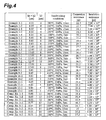
Fig. 4 is a table showing the conditions, and connection resistance and insulation resistance values for Example 1-1 to 12-2 and Comparative Example 1-1 to 4-2. - 10: Liquid crystal display device, 12: circuit member (first circuit member), 12a: first board, 12b: first circuit electrode, 14: flexible wiring board (second circuit member), 14a: second board, 14b: second circuit electrode, 16: anisotropic conductive film for circuit connection, 18: solder resist (insulating layer).
- Preferred embodiments of the invention will now be explained with reference to the accompanying drawings. Throughout the explanation, identical or similarly functioning elements will be referred to by like reference numerals and will be explained only once.
- The construction of a liquid
crystal display device 10 in which the circuit connecting method of the invention was applied will be explained first, with reference toFig. 1 andFig. 2 . The liquidcrystal display device 10 comprises a circuit member (first circuit member) 12, a flexible wiring board (second circuit member) 14, and an anisotropic conductive film forcircuit connection 16. - The
circuit member 12 comprises a glass substrate (first board) 12a and circuit electrodes (first circuit electrodes) 12b. Theglass substrate 12a, together with another glass substrate (not shown), sandwiches the liquid crystal layer to form a liquid crystal panel. - The
circuit electrodes 12b are a transparent electrode made of ITO (indium tin oxide), for example, and they are formed on the main surface of theglass substrate 12a. Thecircuit electrodes 12b have the function of applying a voltage to the liquid crystals in the liquid crystal layer to drive the liquid crystals. The height h1 of thecircuit electrodes 12b may be about 0.05 µm-0.7 µm, for example. - The
flexible wiring board 14 comprises a base (second board) 14a and circuit electrodes (second circuit electrodes) 14b. Thebase 14a may be a polyimide film, for example. Thecircuit electrodes 14b are composed of Cu with a Sn plating, for example, and they are formed on the main surface of thebase 14a. - On the
flexible wiring board 14, on the sections of thecircuit electrodes 14b other than the section that is connected to thecircuit electrodes 12b, there is provided a solder resist (insulating layer) 18 as a protecting member to protect thecircuit electrodes 14b. The height h2 of thecircuit electrodes 14b may be about 5 µm-100 µm, for example. - The anisotropic conductive film for
circuit connection 16 hasconductive particles 16b evenly dispersed in a thermosetting adhesive 16a. The anisotropic conductive film forcircuit connection 16 has anisotropic conductivity such that it exhibits conductivity in the thickness direction in which force is applied, but exhibits no conductivity in the in-plane direction. The anisotropic conductive film forcircuit connection 16 may be any adhesive film containingconductive particles 16b, without any particular restrictions, and using thethermosetting adhesive 16a as mentioned above results in a more notable effect of the invention with higher temperature and shorter time for the circuit connection conditions. - The anisotropic conductive film for
circuit connection 16 bonds thecircuit member 12 andflexible wiring board 14. Specifically, the anisotropic conductive film forcircuit connection 16 is disposed between thecircuit member 12 and part of theflexible wiring board 14 connected to thecircuit member 12 and part of the solder resist 18, with a part of the anisotropic conductive film forcircuit connection 16 overlapping a part of thesolder resist 18. - As shown in detail in
Fig. 2 , the section of the anisotropic conductive film forcircuit connection 16 other than the section that is between thecircuit electrodes 12b andcircuit electrodes 14b fills the area between the adjacent electrodes among each of thecircuit electrodes 12b and the adjacent electrodes among each of thecircuit electrodes 14b, so that thecircuit electrodes 12b andcircuit electrodes 14b become electrically connected by theconductive particles 16b. - A method for producing the liquid
crystal display device 10 will now be explained with reference toFig. 3 . - First, a circuit member 12 (liquid crystal panel) having a
circuit electrode 12b formed on the main surface of aglass substrate 12a is prepared. Aflexible wiring board 14 is also prepared havingcircuit electrodes 14b formed on the main surface of abase 14a and having a solder resist 18 provided on the sections of thecircuit electrodes 14b other than the section that are connected to thecircuit electrodes 12b. - An anisotropic conductive film for
circuit connection 16 is also prepared. The anisotropic conductive film forcircuit connection 16 has a thickness h3 before connection of thecircuit member 12 andflexible wiring board 14, which is no greater than the total of the height h1 of thecircuit electrodes 12b and the height h2 of thecircuit electrodes 14b, and it may be 5.05 µm-100.7 µm, for example. - The thickness h3 of the anisotropic conductive film for
circuit connection 16 is preferably no greater than 70% of the total of the height h1 of thecircuit electrodes 12b and the height h2 of thecircuit electrodes 14b. This will further promote elimination of the part of the anisotropic conductive film forcircuit connection 16 between thefirst circuit electrodes 12b andsecond circuit electrodes 14b, for between the adjacent electrodes among each of thefirst circuit electrodes 12b and the adjacent electrodes among each of thesecond circuit electrodes 14b. - Also, the thickness h3 of the anisotropic conductive film for
circuit connection 16 is preferably at least 50% of the total of the height h1 of thecircuit electrodes 12b and the height h2 of thecircuit electrodes 14b. If the thickness h3 of the anisotropic conductive film forcircuit connection 16 is less than 50% of the total of the height h1 of thefirst circuit electrodes 12b and the height h2 of thesecond circuit electrodes 14b, the anisotropic conductive film forcircuit connection 16 will not sufficiently fill between the adjacent electrodes among each of thefirst circuit electrodes 12b and the adjacent electrodes among each of thesecond circuit electrodes 14b, thus lowering the bonding strength between thefirst circuit member 12b andsecond circuit member 14b while also tending to reduce the electrical insulating property between the adjacent electrodes among each of thefirst circuit electrodes 12b and the electrical insulating property between the adjacent electrodes among each of thesecond circuit electrodes 14b. - Next, the anisotropic conductive film for
circuit connection 16 is disposed between thecircuit member 12 andflexible wiring board 14, and the anisotropic conductive film forcircuit connection 16 is sandwiched by thecircuit member 12 andflexible wiring board 14 so that part of the anisotropic conductive film forcircuit connection 16 overlaps with part of thesolder resist 18. Specifically, thecircuit member 12 andflexible wiring board 14 are bonded via the anisotropic conductive film forcircuit connection 16 in this manner to complete the liquid crystal display device. - According to this embodiment, the
circuit member 12 andflexible wiring board 14 are bonded via the anisotropic conductive film forcircuit connection 16, and the thickness h3 of the anisotropic conductive film forcircuit connection 16 is no greater than the total of the height h1 of thecircuit electrodes 12b and the height h2 of thecircuit electrodes 14b. Thus, when thecircuit member 12 andflexible wiring board 14 are bonded, the part of the anisotropic conductive film forcircuit connection 16 between thecircuit electrodes 12b andcircuit electrodes 14b remain between thecircuit electrodes 12b andcircuit electrodes 14b only in the amount required to electrically connect and bond thecircuit electrodes 12b andcircuit electrodes 14b, while the rest is eliminated between the adjacent electrodes among each of thecircuit electrodes 12b and the adjacent electrodes among each of thecircuit electrodes 14b. As a result, even if thecircuit member 12 andflexible wiring board 14 are bonded via the anisotropic conductive film forcircuit connection 16 so that part of the anisotropic conductive film forcircuit connection 16 overlaps a part of the solder resist 18, it is possible to sufficiently reduce the connection resistance between thecircuit electrodes 12b andcircuit electrodes 14b that are electrically connected via the anisotropic conductive film forcircuit connection 16. - The above detailed explanation of a preferred embodiment of the invention is not intended to restrict the scope of the invention to this particular embodiment. For example, the invention can also be applied to display devices other than liquid crystal display devices (such as plasma displays or organic EL displays).
- Also, although the circuit member 12 (
glass substrate 12a) andflexible wiring board 14 are bonded by the anisotropic conductive film forcircuit connection 16 in this embodiment, two glass substrates may be bonded instead, or two flexible wiring boards may be bonded instead. Different circuit members other than these may also be bonded together. - The present invention will now be explained in greater detail based on Examples 1-1 to 12-2 and Comparative Examples 1-1 to 4-2, with the understanding that these examples are in no way limitative on the invention.
- First, a
circuit member 12 was prepared havingITO circuit electrodes 12b (film thickness: h1 = 50 nm, surface resistance: <20 Ω) formed on the surface of aglass substrate 12a (thickness: 1.1 mm). The line widths of thecircuit electrodes 12b were 25 µm and the pitch was 50 µm. - There was also prepared a
flexible wiring board 14 having Sn-plated Cufoil circuit electrodes 14b (thickness: h2 = 8 µm) formed on the surface of apolyimide film base 14a (thickness: 38 µm). The line widths of thecircuit electrodes 14b were 18 µm and the pitch was 50 µm. Also, a solder resist 18 ("SN-9000" solder resist by Hitachi Chemical Co., Ltd.) was provided as a protecting member to protect thecircuit electrodes 14b, on the sections of thecircuit electrodes 14b other than the sections that are connected to thecircuit electrodes 12b. The thickness of the solder resist 18 was 30 µm and the width was 10 mm. - There was additionally prepared an anisotropic conductive film for
circuit connection 16 with a thickness h3 of 8 µm ("ANISOLM: AC-7206U-8" anisotropic conductive film by Hitachi Chemical Co., Ltd.). - The
circuit member 12 andflexible wiring board 14 were positioned at a circuit bonding width of 1.5 mm and the anisotropic conductive film forcircuit connection 16 was sandwiched by thecircuit member 12 andflexible wiring board 14 and hot pressed at 180°C, 3 MPa for 15 seconds to obtain a liquidcrystal display device 10 for Example 1-1. The anisotropic conductive film forcircuit connection 16 and solder resist 18 had an overlap of 0.5 mm. - A liquid
crystal display device 10 for Example 1-2 was obtained in the same manner as Example 1-1, except that the anisotropic conductive film forcircuit connection 16 was sandwiched by thecircuit member 12 andflexible wiring board 14 and hot pressed at 210°C, 3 MPa for 15 seconds. - A liquid
crystal display device 10 for Example 2-1 was obtained in the same manner as Example 1-1, except that the anisotropic conducive film forcircuit connection 16 had a thickness h3 of 6 µm ("ANISOLM: AC-7206U-6" anisotropic conductive film by Hitachi Chemical Co., Ltd.). - A liquid
crystal display device 10 for Example 2-2 was obtained in the same manner as Example 1-1, except that the anisotropic conductive film forcircuit connection 16 had a thickness h3 of 6 µm ("ANISOLM: AC-7206U-6" anisotropic conductive film by Hitachi Chemical Co., Ltd.), and the anisotropic conductive film forcircuit connection 16 was sandwiched by thecircuit member 12 andflexible wiring board 14 and hot pressed at 210°C, 3 MPa for 15 seconds. - A liquid
crystal display device 10 for Example 3-1 was obtained in the same manner as Example 1-1, except that the anisotropic conductive film forcircuit connection 16 had a thickness h3 of 8 µm ("ANISOLM: AC-11000Y-8" anisotropic conductive film by Hitachi Chemical Co., Ltd.), and the anisotropic conductive film forcircuit connection 16 was sandwiched by thecircuit member 12 andflexible wiring board 14 and hot pressed at 180°C, 3 MPa for 5 seconds. - A liquid
crystal display device 10 for Example 3-2 was obtained in the same manner as Example 1-1, except that the anisotropic conductive film forcircuit connection 16 had a thickness h3 of 8 µm ("ANISOLM: AC-11000Y-8" anisotropic conductive film by Hitachi Chemical Co., Ltd.), and the anisotropic conductive film forcircuit connection 16 was sandwiched by thecircuit member 12 andflexible wiring board 14 and hot pressed at 210°C, 3 MPa for 5 seconds. - A liquid
crystal display device 10 for Example 4-1 was obtained in the same manner as Example 1-1, except that the anisotropic conductive film forcircuit connection 16 had a thickness h3 of 6 µm ("ANISOLM: AC-11000Y-6" anisotropic conductive film by Hitachi Chemical Co., Ltd.), and the anisotropic conductive film forcircuit connection 16 was sandwiched by thecircuit member 12 andflexible wiring board 14 and hot pressed at 180°C, 3 MPa for 5 seconds. - A liquid
crystal display device 10 for Example 4-2 was obtained in the same manner as Example 1-1, except that the anisotropic conductive film forcircuit connection 16 had a thickness h3 of 6 µm ("ANISOLM: AC-11000Y-6" anisotropic conductive film by Hitachi Chemical Co., Ltd.), and the anisotropic conductive film forcircuit connection 16 was sandwiched by thecircuit member 12 andflexible wiring board 14 and hot pressed at 210°C, 3 MPa for 5 seconds. - First, a
circuit member 12 was prepared havingITO circuit electrodes 12b (film thickness: h1 = 50 nm, surface resistance: <20 Ω) formed on the surface of aglass substrate 12a (thickness: 1.1 mm). The line widths of thecircuit electrodes 12b were 25 µm and the pitch was 50 µm. - There was also prepared a
flexible wiring board 14 having Sn-plated Cufoil circuit electrodes 14b (thickness: h2 = 12 µm) formed on the surface of apolyimide film base 14a (thickness: 38 µm). The line widths of thecircuit electrodes 14b were 18 µm and the pitch was 50 µm. Also, a solder resist 18 ("SN-9000" solder resist by Hitachi Chemical Co., Ltd.) was provided as a protecting member to protect thecircuit electrodes 14b, on the sections of thecircuit electrodes 14b other than the sections that are connected to thecircuit electrodes 12b. The thickness of the solder resist 18 was 30 µm and the width was 10 mm. - There was additionally prepared an anisotropic conductive film for
circuit connection 16 with a thickness h3 of 12 µm ("ANISOLM: AC-7206U-12" anisotropic conductive film by Hitachi Chemical Co., Ltd.). - The
circuit member 12 andflexible wiring board 14 were positioned at a circuit bonding width of 1.5 mm and the anisotropic conductive film forcircuit connection 16 was sandwiched by thecircuit member 12 andflexible wiring board 14 and hot pressed at 180°C, 3 MPa for 15 seconds to obtain a liquidcrystal display device 10 for Example 5-1. The anisotropic conductive film forcircuit connection 16 and solder resist 18 had an overlap of 0.5 mm. - A liquid
crystal display device 10 for Example 5-2 was obtained in the same manner as Example 5-1, except that the anisotropic conductive film forcircuit connection 16 was sandwiched by thecircuit member 12 andflexible wiring board 14 and hot pressed at 210°C, 3 MPa for 15 seconds. - A liquid
crystal display device 10 for Example 6-1 was obtained in the same manner as Example 5-1, except that the anisotropic conductive film forcircuit connection 16 had a thickness h3 of 8 µm ("ANISOLM: AC-7206U-8" anisotropic conductive film by Hitachi Chemical Co., Ltd.). - A liquid
crystal display device 10 for Example 6-2 was obtained in the same manner as Example 5-1, except that the anisotropic conductive film forcircuit connection 16 had a thickness h3 of 8 µm ("ANISOLM: AC-7206U-8" anisotropic conductive film by Hitachi Chemical Co., Ltd.), and the anisotropic conductive film forcircuit connection 16 was sandwiched by thecircuit member 12 andflexible wiring board 14 and hot pressed at 210°C, 3 MPa for 15 seconds. - A liquid
crystal display device 10 for Example 7-1 was obtained in the same manner as Example 5-1, except that the anisotropic conductive film forcircuit connection 16 had a thickness h3 of 12 µm ("ANISOLM: AC-11000Y-12" anisotropic conductive film by Hitachi Chemical Co., Ltd.), and the anisotropic conductive film forcircuit connection 16 was sandwiched by thecircuit member 12 andflexible wiring board 14 and hot pressed at 180°C, 3 MPa for 5 seconds. - A liquid
crystal display device 10 for Example 7-2 was obtained in the same manner as Example 5-1, except that the anisotropic conductive film forcircuit connection 16 had a thickness h3 of 12 µm ("ANISOLM: AC-11000Y-12" anisotropic conductive film by Hitachi Chemical Co., Ltd.), and the anisotropic conductive film forcircuit connection 16 was sandwiched by thecircuit member 12 andflexible wiring board 14 and hot pressed at 210°C, 3 MPa for 5 seconds. - A liquid
crystal display device 10 for Example 8-1 was obtained in the same manner as Example 5-1, except that the anisotropic conductive film forcircuit connection 16 had a thickness h3 of 8 µm ("ANISOLM: AC-11000Y-8" anisotropic conductive film by Hitachi Chemical Co., Ltd.), and the anisotropic conductive film forcircuit connection 16 was sandwiched by thecircuit member 12 andflexible wiring board 14 and hot pressed at 180°C, 3 MPa for 5 seconds. - A liquid
crystal display device 10 for Example 8-2 was obtained in the same manner as Example 5-1, except that the anisotropic conductive film forcircuit connection 16 had a thickness h3 of 8 µm ("ANISOLM: AC-11000Y-8" anisotropic conductive film by Hitachi Chemical Co., Ltd.), and the anisotropic conductive film forcircuit connection 16 was sandwiched by thecircuit member 12 andflexible wiring board 14 and hot pressed at 210°C, 3 MPa for 5 seconds. - A liquid
crystal display device 10 for Example 9-1 was obtained in the same manner as Example 1-1, except that the anisotropic conductive film forcircuit connection 16 had a thickness h3 of 3 µm ("ANISOLM: AC-7206U-3" anisotropic conductive film by Hitachi Chemical Co., Ltd.). - A liquid
crystal display device 10 for Example 9-2 was obtained in the same manner as Example 1-1, except that the anisotropic conductive film forcircuit connection 16 had a thickness h3 of 3 µm ("ANISOLM: AC-7206U-3" anisotropic conductive film by Hitachi Chemical Co., Ltd.), and the anisotropic conductive film forcircuit connection 16 was sandwiched by thecircuit member 12 andflexible wiring board 14 and hot pressed at 210°C, 3 MPa for 15 seconds. - A liquid
crystal display device 10 for Example 10-1 was obtained in the same manner as Example 1-1, except that the anisotropic conductive film forcircuit connection 16 had a thickness h3 of 3 µm ("ANISOLM: AC-11000Y-3" anisotropic conductive film by Hitachi Chemical Co., Ltd.), and the anisotropic conductive film forcircuit connection 16 was sandwiched by thecircuit member 12 andflexible wiring board 14 and hot pressed at 180°C, 3 MPa for 5 seconds. - A liquid
crystal display device 10 for Example 10-2 was obtained in the same manner as Example 1-1, except that the anisotropic conductive film forcircuit connection 16 had a thickness h3 of 3 µm ("ANISOLM: AC-11000Y-3" anisotropic conductive film by Hitachi Chemical Co., Ltd.), and the anisotropic conductive film forcircuit connection 16 was sandwiched by thecircuit member 12 andflexible wiring board 14 and hot pressed at 210°C, 3 MPa for 5 seconds. - A liquid
crystal display device 10 for Example 11-1 was obtained in the same manner as Example 1-1, except that the anisotropic conductive film forcircuit connection 16 had a thickness h3 of 4 µm ("ANISOLM: AC-7206U-4" anisotropic conductive film by Hitachi Chemical Co., Ltd.). - A liquid
crystal display device 10 for Example 11-2 was obtained in the same manner as Example 1-1, except that the anisotropic conductive film forcircuit connection 16 had a thickness h3 of 4 µm ("ANISOLM: AC-7206U-4" anisotropic conductive film by Hitachi Chemical Co., Ltd.), and the anisotropic conductive film forcircuit connection 16 was sandwiched by thecircuit member 12 andflexible wiring board 14 and hot pressed at 210°C, 3 MPa for 15 seconds. - A liquid
crystal display device 10 for Example 12-1 was obtained in the same manner as Example 1-1, except that the anisotropic conductive film forcircuit connection 16 had a thickness h3 of 14 µm ("ANISOLM: AC-11000Y-14" anisotropic conductive film by Hitachi Chemical Co., Ltd.), and the anisotropic conductive film forcircuit connection 16 was sandwiched by thecircuit member 12 andflexible wiring board 14 and hot pressed at 180°C, 3 MPa for 5 seconds. - A liquid
crystal display device 10 for Example 12-2 was obtained in the same manner as Example 1-1, except that the anisotropic conductive film forcircuit connection 16 had a thickness h3 of 14 µm ("ANISOLM: AC-11000Y-14" anisotropic conductive film by Hitachi Chemical Co., Ltd.), and the anisotropic conductive film forcircuit connection 16 was sandwiched by thecircuit member 12 andflexible wiring board 14 and hot pressed at 210°C, 3 MPa for 5 seconds. - A liquid crystal display device for Comparative Example 1-1 was obtained in the same manner as Example 1-1, except that the anisotropic conductive film for
circuit connection 16 had a thickness h3 of 12 µm ("ANISOLM: AC-7206U-12" anisotropic conductive film by Hitachi Chemical Co., Ltd.). - A liquid crystal display device for Comparative Example 1-2 was obtained in the same manner as Example 1-1, except that the anisotropic conductive film for
circuit connection 16 had a thickness h3 of 12 µm ("ANISOLM: AC-7206U-12" anisotropic conductive film by Hitachi Chemical Co., Ltd.), and the anisotropic conductive film forcircuit connection 16 was sandwiched by thecircuit member 12 andflexible wiring board 14 and hot pressed at 210°C, 3 MPa for 15 seconds. - A liquid crystal display device for Comparative Example 2-1 was obtained in the same manner as Example 1-1, except that the anisotropic conductive film for
circuit connection 16 had a thickness h3 of 12 µm ("ANISOLM: AC-11000Y-12" anisotropic conductive film by Hitachi Chemical Co., Ltd.), and the anisotropic conductive film forcircuit connection 16 was sandwiched by thecircuit member 12 andflexible wiring board 14 and hot pressed at 180°C, 3 MPa for 5 seconds. - A liquid crystal display device for Comparative Example 2-2 was obtained in the same manner as Example 1-1, except that the anisotropic conductive film for
circuit connection 16 had a thickness h3 of 12 µm ("ANISOLM: AC-11000Y-12" anisotropic conductive film by Hitachi Chemical Co., Ltd.), and the anisotropic conductive film forcircuit connection 16 was sandwiched by thecircuit member 12 andflexible wiring board 14 and hot pressed at 210°C, 3 MPa for 5 seconds. - A liquid crystal display device for Comparative Example 3-1 was obtained in the same manner as Example 1-1, except that the anisotropic conductive film for
circuit connection 16 had a thickness h3 of 14 µm ("ANISOLM: AC-7206U-14" anisotropic conductive film by Hitachi Chemical Co., Ltd.). - A liquid crystal display device for Comparative Example 3-2 was obtained in the same manner as Example 1-1, except that the anisotropic conductive film for
circuit connection 16 had a thickness h3 of 14 µm ("ANISOLM: AC-7206U-14" anisotropic conductive film by Hitachi Chemical Co., Ltd.), and the anisotropic conductive film forcircuit connection 16 was sandwiched by thecircuit member 12 andflexible wiring board 14 and hot pressed at 210°C, 3 MPa for 15 seconds. - A liquid crystal display device for Comparative Example 4-1 was obtained in the same manner as Example 1-1, except that the anisotropic conductive film for
circuit connection 16 had a thickness h3 of 4 µm ("ANISOLM: AC-11000Y-4" anisotropic conductive film by Hitachi Chemical Co., Ltd.), and the anisotropic conductive film forcircuit connection 16 was sandwiched by thecircuit member 12 andflexible wiring board 14 and hot pressed at 180°C, 3 MPa for 5 seconds. - A liquid crystal display device for Comparative Example 4-2 was obtained in the same manner as Example 1-1, except that the anisotropic conductive film for
circuit connection 16 had a thickness h3 of 4 µm ("ANISOLM: AC-11000Y-4" anisotropic conductive film by Hitachi Chemical Co., Ltd.), and the anisotropic conductive film forcircuit connection 16 was sandwiched by thecircuit member 12 andflexible wiring board 14 and hot pressed at 210°C, 3 MPa for 5 seconds. - For the liquid
crystal display device 10 of each of Examples 1-1 to 12-2 and the liquid crystal display device of each of Comparative Examples 1-1 to 4-2, obtained as described above, the connection resistance value between thecircuit electrodes Fig. 4 . - (Measurement of insulation resistance between adjacent circuits) For the liquid
crystal display device 10 of each of Examples 1-1 to 12-2 and the liquid crystal display device of each of Comparative Examples 1-1 to 4-2, obtained as described above, the insulation resistance between adjacent electrodes among thecircuit electrodes 12b and between adjacent electrodes among thecircuit electrodes 14b were measured with an insulation resistance meter 500 hours after high-temperature, high-humidity test treatment at 85°C/85% RH. The results of the insulation resistance measurement are shown inFig. 4 . - In Examples 1-1 to 4-2, the connection resistance values were all 30 ±2 Ω and the insulation resistance values were all 108 Ω or greater. In Examples 5-1 to 8-2, the connection resistance values were all no greater than 30 Ω and the insulation resistance values were all 108 Ω or greater. In Examples 9-1 and 9-2,the connection resistance values were both 30 ±2 Ω and the insulation resistance values were both on the order of 105 Ω. In Examples 10-1 to 12-2, the connection resistance values were all no greatr than 30 Ω and the insulation resistance values were all on the order of 104-105 Ω.
- In Comparative Examples 1-1 to 4-2, however, the connection resistance values were all no less than 108 Ω while the insulation resistance values were all 35 Ω or greater.
- With the liquid
crystal display devices 10 of Examples 1-1 to 8-2, the connection resistance between thecircuit electrodes circuit electrodes 12b and between adjacent electrodes among thecircuit electrodes 14b was sufficiently high, even 500 hours after the high-temperature, high-humidity test treatment, thus confirming that long-term reliability was assured. With the liquidcrystal display devices 10 of Examples 9-1 to 12-2, the connection resistance between thecircuit electrodes circuit electrodes 12b and between adjacent electrodes among thecircuit electrodes 14b was too low 500 hours after the high-temperature, high-humidity test treatment, thus confirming that the long-term reliability was inferior.
Claims (5)
- A circuit connecting method comprising
a step of preparing a first circuit member having first circuit electrodes formed on the main surface of a first board,
a step of preparing a second circuit member having second circuit electrodes formed on the main surface of a second board, with an insulating layer provided on the sections of the second circuit electrodes other than the sections that are connected to the first circuit electrodes and
a step of bonding the first circuit member and second circuit member via an anisotropic conductive film for circuit connection so that part of the anisotropic conductive film for circuit connection overlaps part of the insulating layer, for electrical connection between the first circuit electrodes and second circuit electrodes,
wherein the thickness of the anisotropic conductive film for circuit connection is no greater than the total of the height of the first circuit electrodes and the height of the second circuit electrodes. - The circuit connecting method according to claim 1, wherein the thickness of the anisotropic conductive film for circuit connection is no greater than 70% of the total of the height of the first circuit electrodes and the height of the second circuit electrodes.
- The circuit connecting method according to claim 1 or 2, wherein the thickness of the anisotropic conductive film for circuit connection is at least 50% of the total of the height of the first circuit electrodes and the height of the second circuit electrodes.
- The circuit connecting method according to any one of claims 1 to 3, wherein at least one of the first circuit member and second circuit member is flexible wiring boards.
- The circuit connecting method according to any one of claims 1 to 3, wherein
the material of the first board is glass, and
the second circuit member is a flexible wiring board.
Applications Claiming Priority (2)
| Application Number | Priority Date | Filing Date | Title |
|---|---|---|---|
| JP2007281611 | 2007-10-30 | ||
| PCT/JP2008/051960 WO2009057332A1 (en) | 2007-10-30 | 2008-02-06 | Circuit connecting method |
Publications (2)
| Publication Number | Publication Date |
|---|---|
| EP2205052A1 true EP2205052A1 (en) | 2010-07-07 |
| EP2205052A4 EP2205052A4 (en) | 2011-03-09 |
Family
ID=40590736
Family Applications (1)
| Application Number | Title | Priority Date | Filing Date |
|---|---|---|---|
| EP08710856A Withdrawn EP2205052A4 (en) | 2007-10-30 | 2008-02-06 | Circuit connecting method |
Country Status (7)
| Country | Link |
|---|---|
| US (1) | US8132319B2 (en) |
| EP (1) | EP2205052A4 (en) |
| JP (2) | JP2009135388A (en) |
| KR (1) | KR101151200B1 (en) |
| CN (1) | CN101653052B (en) |
| TW (1) | TW200919057A (en) |
| WO (1) | WO2009057332A1 (en) |
Families Citing this family (14)
| Publication number | Priority date | Publication date | Assignee | Title |
|---|---|---|---|---|
| WO2009037964A1 (en) * | 2007-09-20 | 2009-03-26 | Sony Chemical & Information Device Corporation | Anisotropic conductive film and its production method, and bonded body employing anisotropic conductive film |
| JP5140816B2 (en) * | 2009-03-31 | 2013-02-13 | デクセリアルズ株式会社 | JOINT BODY AND MANUFACTURING METHOD |
| JP2011059149A (en) * | 2009-09-07 | 2011-03-24 | Hitachi Displays Ltd | Electronic device |
| JP5465121B2 (en) * | 2010-07-29 | 2014-04-09 | 東海ゴム工業株式会社 | Wiring body connection structure |
| JP5695881B2 (en) * | 2010-10-28 | 2015-04-08 | デクセリアルズ株式会社 | Electronic component connection method and connection structure |
| JP5779931B2 (en) * | 2011-03-24 | 2015-09-16 | 富士通株式会社 | Manufacturing method of semiconductor device |
| KR102697500B1 (en) | 2013-11-19 | 2024-08-21 | 데쿠세리아루즈 가부시키가이샤 | Anisotropic electroconductive film and connection structure |
| JP6119718B2 (en) * | 2013-11-19 | 2017-04-26 | デクセリアルズ株式会社 | Anisotropic conductive film and connection structure |
| JP2016178225A (en) | 2015-03-20 | 2016-10-06 | デクセリアルズ株式会社 | Anisotropic conductive connection structure, anisotropic conductive connection method, and anisotropic conductive adhesive |
| CN105555023B (en) * | 2016-02-03 | 2016-11-09 | 武汉华尚绿能科技股份有限公司 | High conducting clear glass base circuit board |
| JP6778585B2 (en) * | 2016-11-02 | 2020-11-04 | 日東電工株式会社 | Wiring circuit board and its manufacturing method |
| CN108366487A (en) * | 2018-01-30 | 2018-08-03 | 业成科技(成都)有限公司 | Circuit board connected structure and circuit board joint method |
| CN112752402B (en) * | 2019-10-29 | 2022-10-18 | 群创光电股份有限公司 | Flexible circuit board and display device |
| CN117425291B (en) * | 2023-10-27 | 2024-05-03 | 浙江晶引电子科技有限公司 | High-reliability electrical connection method of ultrathin flexible film packaging substrate |
Family Cites Families (18)
| Publication number | Priority date | Publication date | Assignee | Title |
|---|---|---|---|---|
| US4554033A (en) * | 1984-10-04 | 1985-11-19 | Amp Incorporated | Method of forming an electrical interconnection means |
| US5502889A (en) * | 1988-06-10 | 1996-04-02 | Sheldahl, Inc. | Method for electrically and mechanically connecting at least two conductive layers |
| US5235741A (en) * | 1989-08-18 | 1993-08-17 | Semiconductor Energy Laboratory Co., Ltd. | Electrical connection and method for making the same |
| JP2657429B2 (en) * | 1990-04-09 | 1997-09-24 | 株式会社ミクロ技術研究所 | Circuit mounting method for circuit board and circuit board used for the method |
| JPH04301817A (en) * | 1991-03-29 | 1992-10-26 | Rohm Co Ltd | Liquid crystal display device and its production |
| JPH05303107A (en) * | 1992-04-28 | 1993-11-16 | Nec Kagoshima Ltd | Manufacture of liquid crystal display device |
| JPH09148731A (en) * | 1995-11-17 | 1997-06-06 | Fujitsu Ltd | Method for manufacturing connection structure between wiring boards |
| US5839188A (en) * | 1996-01-05 | 1998-11-24 | Alliedsignal Inc. | Method of manufacturing a printed circuit assembly |
| US5903056A (en) * | 1997-04-21 | 1999-05-11 | Lucent Technologies Inc. | Conductive polymer film bonding technique |
| JP3678547B2 (en) | 1997-07-24 | 2005-08-03 | ソニーケミカル株式会社 | Multilayer anisotropic conductive adhesive and method for producing the same |
| JPH11148058A (en) * | 1997-11-17 | 1999-06-02 | Seiko Epson Corp | Anisotropic conductive adhesive, liquid crystal display device and electronic equipment using the same |
| JP3804269B2 (en) | 1998-03-31 | 2006-08-02 | カシオ計算機株式会社 | Flexible wiring board bonding structure |
| JP2001031929A (en) * | 1999-07-21 | 2001-02-06 | Sony Chem Corp | Connected structure |
| JP3792554B2 (en) * | 2001-03-26 | 2006-07-05 | シャープ株式会社 | Display module and flexible wiring board connection method |
| JP4492148B2 (en) * | 2004-02-18 | 2010-06-30 | 日立化成工業株式会社 | Circuit connection method |
| JP2005310905A (en) | 2004-04-19 | 2005-11-04 | Sharp Corp | Electronic component connection structure |
| JP2006012992A (en) * | 2004-06-23 | 2006-01-12 | Sharp Corp | Circuit board electrode connection structure |
| JP4968665B2 (en) * | 2006-04-18 | 2012-07-04 | Nltテクノロジー株式会社 | Flat display panel and connection structure |
-
2008
- 2008-01-29 JP JP2008017993A patent/JP2009135388A/en active Pending
- 2008-02-06 US US12/740,801 patent/US8132319B2/en not_active Expired - Fee Related
- 2008-02-06 JP JP2009538956A patent/JP5131279B2/en not_active Expired - Fee Related
- 2008-02-06 CN CN2008800113074A patent/CN101653052B/en not_active Expired - Fee Related
- 2008-02-06 WO PCT/JP2008/051960 patent/WO2009057332A1/en not_active Ceased
- 2008-02-06 KR KR1020097021228A patent/KR101151200B1/en not_active Expired - Fee Related
- 2008-02-06 EP EP08710856A patent/EP2205052A4/en not_active Withdrawn
- 2008-02-12 TW TW097104907A patent/TW200919057A/en not_active IP Right Cessation
Also Published As
| Publication number | Publication date |
|---|---|
| US20100263208A1 (en) | 2010-10-21 |
| KR101151200B1 (en) | 2012-06-08 |
| JPWO2009057332A1 (en) | 2011-03-10 |
| KR20090122282A (en) | 2009-11-26 |
| JP2009135388A (en) | 2009-06-18 |
| JP5131279B2 (en) | 2013-01-30 |
| CN101653052B (en) | 2012-11-14 |
| CN101653052A (en) | 2010-02-17 |
| WO2009057332A1 (en) | 2009-05-07 |
| TW200919057A (en) | 2009-05-01 |
| EP2205052A4 (en) | 2011-03-09 |
| US8132319B2 (en) | 2012-03-13 |
| TWI372935B (en) | 2012-09-21 |
Similar Documents
| Publication | Publication Date | Title |
|---|---|---|
| US8132319B2 (en) | Circuit connecting method | |
| EP3779583B1 (en) | Light control unit | |
| WO2004061640A1 (en) | Narrow-frame touch panel | |
| US20110169791A1 (en) | Display device | |
| US20140069696A1 (en) | Methods and apparatus for attaching multi-layer flex circuits to substrates | |
| CN102844936B (en) | The method of attachment of electronic unit and connection structural bodies | |
| Watanabe et al. | Recent advances of interconnection technologies using anisotropic conductive films in flat panel display applications | |
| US8314787B2 (en) | Display device | |
| TW200930169A (en) | Flexible film and display device comprising the same | |
| CN106604540A (en) | Circuit board | |
| JP7047724B2 (en) | Dimming cell, dimming body and moving body | |
| US7279794B2 (en) | Semiconductor device and electronic device, and methods for manufacturing thereof | |
| EP2466631A1 (en) | Substrate module and manufacturing method thereof | |
| CN100452379C (en) | Display panel and control circuit packaging structure thereof | |
| CN102170753A (en) | Circuit board pin structure | |
| CN220965245U (en) | Flexible circuit structure and display panel | |
| CN120076158B (en) | Display panel, display panel manufacturing method and display module | |
| CN113611213A (en) | Chip on film and display device | |
| Matsuda et al. | Interconnection technologies of anisotropic conductive films and their application to flexible electronics | |
| JP4626952B2 (en) | Adhesive sheet | |
| CN118053879A (en) | Bonding structures, display modules and electronic devices | |
| JPH06222373A (en) | Circuit connection method | |
| JP2004325751A (en) | Flexible wiring board for liquid crystal display panel | |
| JPH0442942A (en) | Mounting structure of semiconductor | |
| TWM425290U (en) | Liquid crystal display panel |
Legal Events
| Date | Code | Title | Description |
|---|---|---|---|
| PUAI | Public reference made under article 153(3) epc to a published international application that has entered the european phase |
Free format text: ORIGINAL CODE: 0009012 |
|
| 17P | Request for examination filed |
Effective date: 20100310 |
|
| AK | Designated contracting states |
Kind code of ref document: A1 Designated state(s): AT BE BG CH CY CZ DE DK EE ES FI FR GB GR HR HU IE IS IT LI LT LU LV MC MT NL NO PL PT RO SE SI SK TR |
|
| AX | Request for extension of the european patent |
Extension state: AL BA MK RS |
|
| DAX | Request for extension of the european patent (deleted) | ||
| A4 | Supplementary search report drawn up and despatched |
Effective date: 20110204 |
|
| GRAP | Despatch of communication of intention to grant a patent |
Free format text: ORIGINAL CODE: EPIDOSNIGR1 |
|
| STAA | Information on the status of an ep patent application or granted ep patent |
Free format text: STATUS: THE APPLICATION IS DEEMED TO BE WITHDRAWN |
|
| 18D | Application deemed to be withdrawn |
Effective date: 20121030 |