EP2204906B1 - Verteilter aktiver Transformatorverstärker mit differentiellem Leistungskombinierer - Google Patents
Verteilter aktiver Transformatorverstärker mit differentiellem Leistungskombinierer Download PDFInfo
- Publication number
- EP2204906B1 EP2204906B1 EP09179210A EP09179210A EP2204906B1 EP 2204906 B1 EP2204906 B1 EP 2204906B1 EP 09179210 A EP09179210 A EP 09179210A EP 09179210 A EP09179210 A EP 09179210A EP 2204906 B1 EP2204906 B1 EP 2204906B1
- Authority
- EP
- European Patent Office
- Prior art keywords
- input
- output
- power amplifier
- coupled
- distributed active
- Prior art date
- Legal status (The legal status is an assumption and is not a legal conclusion. Google has not performed a legal analysis and makes no representation as to the accuracy of the status listed.)
- Active
Links
Images


Classifications
-
- H—ELECTRICITY
- H03—ELECTRONIC CIRCUITRY
- H03F—AMPLIFIERS
- H03F3/00—Amplifiers with only discharge tubes or only semiconductor devices as amplifying elements
- H03F3/60—Amplifiers in which coupling networks have distributed constants, e.g. with waveguide resonators
- H03F3/602—Combinations of several amplifiers
- H03F3/604—Combinations of several amplifiers using FET's
-
- H—ELECTRICITY
- H03—ELECTRONIC CIRCUITRY
- H03F—AMPLIFIERS
- H03F1/00—Details of amplifiers with only discharge tubes, only semiconductor devices or only unspecified devices as amplifying elements
- H03F1/02—Modifications of amplifiers to raise the efficiency, e.g. gliding Class A stages, use of an auxiliary oscillation
- H03F1/0205—Modifications of amplifiers to raise the efficiency, e.g. gliding Class A stages, use of an auxiliary oscillation in transistor amplifiers
-
- H—ELECTRICITY
- H03—ELECTRONIC CIRCUITRY
- H03F—AMPLIFIERS
- H03F3/00—Amplifiers with only discharge tubes or only semiconductor devices as amplifying elements
- H03F3/26—Push-pull amplifiers; Phase-splitters therefor
- H03F3/265—Push-pull amplifiers; Phase-splitters therefor with field-effect transistors only
-
- H—ELECTRICITY
- H03—ELECTRONIC CIRCUITRY
- H03F—AMPLIFIERS
- H03F3/00—Amplifiers with only discharge tubes or only semiconductor devices as amplifying elements
- H03F3/45—Differential amplifiers
- H03F3/45071—Differential amplifiers with semiconductor devices only
- H03F3/45076—Differential amplifiers with semiconductor devices only characterised by the way of implementation of the active amplifying circuit in the differential amplifier
- H03F3/45179—Differential amplifiers with semiconductor devices only characterised by the way of implementation of the active amplifying circuit in the differential amplifier using MOSFET transistors as the active amplifying circuit
-
- H—ELECTRICITY
- H03—ELECTRONIC CIRCUITRY
- H03F—AMPLIFIERS
- H03F2200/00—Indexing scheme relating to amplifiers
- H03F2200/534—Transformer coupled at the input of an amplifier
-
- H—ELECTRICITY
- H03—ELECTRONIC CIRCUITRY
- H03F—AMPLIFIERS
- H03F2200/00—Indexing scheme relating to amplifiers
- H03F2200/537—A transformer being used as coupling element between two amplifying stages
-
- H—ELECTRICITY
- H03—ELECTRONIC CIRCUITRY
- H03F—AMPLIFIERS
- H03F2200/00—Indexing scheme relating to amplifiers
- H03F2200/541—Transformer coupled at the output of an amplifier
Definitions
- the present invention relates to a distributed active transformer (DAT) amplifier with fully differential power combiner.
- DAT distributed active transformer
- Power combiners have particular application in the field of radiofrequency power amplifiers, thanks to the characteristic of in-phase summing the output powers of each individual transistor, maintaining the gain and reducing the voltage thereof at the output terminals.
- the radiofrequency power amplifier for wireless mobile telecommunications is certainly the most complicated circuit to design using a silicon substrate and using a CMOS compatible process.
- the reasons for this difficulty are basically two:
- Figure 1 shows the schematic structure of this amplifier 1, comprising four pairs 2 of transistors 3, 4, of an NMOS type, the transistors 3, 4 of each pair 2 having output terminals (drain) connected to four primaries 10 of a distributed active transformer (DAT) 15, proposed herein.
- DAT distributed active transformer
- the primaries 10 are formed by four slabs, here rectangular, each at 90° with respect to the two adjacent slabs so as to extend approximately like the sides of a square.
- a secondary 16 of the DAT 15 is formed by a region extending substantially along the sides of a square, inside the primaries 10, and a side thereof (on the right in the drawing) is interrupted approximately in the middle and is connected to a pair of outputs 18, supplying a differential output voltage Vo.
- the intermediate taps of the primaries 10 are connected to a supply voltage VDD.
- the transistors 3, 4 of each pair 2 are connected, via the drain terminals, between pairs of adjacent primaries 10 and receive, on the respective gate terminals (which define respective input terminals), voltages of opposite sign.
- the common node between the source terminals of the two transistors 3, 4 of each pair is grounded.
- Tuning capacitors 7 extend between the drain terminals of each pair 2 of transistors 3, 4.
- the secondary 16 of the transformer combines in series, via magnetic induction, the differential signal of the primaries 10 and sends it to the output 18.
- the advantages of this known transformer structure are the following:
- Figure 2 shows a practical embodiment of the structure object of patent No. US-B-6 816 012 referred to above, in particular in the case of a 2.4-GHz power amplifier having an output power of 1.9 W at a 2 V supply.
- the amplifier 1 has a double star structure 20 for biasing the gate terminals of the transistors 3, 4.
- the double star structure 20 is formed within the secondary 16 in order to contain the ohmic losses as much as possible and consequently minimize the lengths of the metal paths.
- the double star structure 20 is formed by a first and a second star regions 20a 20b, formed on two separate metal levels and having each four arms 21a, 21b.
- the arms 21a of the first star region 20a are connected to the transistors 3, and the arms 21b of the second star region 20b are connected to the transistors 4.
- each arm 21a, 21b is connected to a respective transistor 3, 4 via wire connections or further metal levels (represented schematically and designated by 22) that extend under or over the secondary 16.
- Each star region 20a, 20b further comprises a respective input arm 22a, 22b, connected to an input transformer 25 arranged outside the DAT amplifier 1 and having input terminals receiving a supply voltage Vi and output terminals connected each to a respective input arm 22a, 22b through wire connections or metal lines 26 extending over or under the secondary 16 (and possibly over or under one of the primaries 10).
- the gate terminals of the transistors 3, 4 are biased through appropriate biasing regions 28, which are substantially L-shaped, the central tap whereof is a signal virtual ground.
- This structure reaches, up to now, the highest power value by using NMOS transistors formed using standard CMOS process, but is not free from disadvantages.
- the circular structure of the secondary 16 (which combines the output powers of the pairs of transistors 3, 4) renders in fact very complicated the design of the network needed for connecting the gate terminals of the transistors 3, 4. In fact:
- the aim of the present invention is thus to provide an amplifier of the DAT type that overcomes the drawbacks of the prior art.
- FIG 3 shows an amplifier 30 of the fully differential power type, with dual distributed active transformer (DDAT).
- the amplifier 30 has, in addition to an output DAT 32 similar to the DAT 15 of Figure 1 , an input DAT 31, specular to and such as to surround or enclose the output DAT 32.
- the amplifier 30 forms a differential dual distributed active transformer (DDDAT) amplifier.
- DDAT differential dual distributed active transformer
- the input DAT 31 comprises a metal region, forming an input primary 35, and a plurality of slab inductors, forming input secondaries 36.
- the input primary 35 extends along the sides of a square having an open side and connected to input terminals 37 receiving a differential input signal Vi.
- the input secondaries 36 are arranged facing the input primary 35, each arranged parallel to and at a distance from a respective side of the input primary 35.
- Each input secondary 36 is thus formed by a slab having its end connected to the gate terminals of first and second transistors 40, 41, similar to the transistors 3, 4 of Figure 1 and forming pairs 39 of transistors, wherein which the transistors 40, 41 connected to a same input secondary 36 are in push-pull configuration.
- the transistors 40, 41 are of an NMOS type, but may also be obtained using a different technology.
- each input secondary 36 is connected with an own end to the gate terminal of a respective first transistor 40 of one pair 39 and with a second end to the gate terminal of a respective second transistor 41 of an adjacent pair 39.
- Each input secondary 36 has an intermediate tap biased at a dc voltage VGG, as may be seen more clearly in Figure 4 .
- the output DAT 32 is formed inside the input DAT 31 and comprises an output secondary 45 similar to the secondary 16 of Figure 1 and four output primaries 46 similar to the primaries 10 of Figure 1 .
- the output primaries 46 are connected to the first and second transistors 40, 41, analogously to Figure 1 for transistors 3, 4.
- the input DAT 31 and the output DAT 32 have the same centre and the same diagonals as the square formed by the output secondary 16.
- the open side of the output secondary 45 is connected to output terminals 48 and is opposite to the side of the input primary 35 connected to the input terminals 37.
- Figure 4 shows the spatial arrangement of the amplifier 30.
- the input DAT 31 and output DAT 32 are formed here in a same metal level.
- the intermediate taps of the output secondaries 46 are connected to an output biasing structure 50 formed in a metal level lower than that of the transformers 31, 32, and the intermediate taps of the input secondaries 36 are connected to an input biasing structure 51 formed in a metal level lower than that of the output biasing structure 50.
- the output biasing structure 50 is formed by a cross having a first arm 50a extending in a first direction (parallel to the axis Y), perpendicular to the sides of the square connected to the input and the output terminals 37, 48, and a second arm 50b, perpendicular to the first arm 50a and extending in a direction parallel to the axis X.
- the second arm 50b of the output biasing structure 50 receives a dc supply voltage VDD, as represented schematically by the voltage generators 58.
- the input biasing structure 51 is formed by a cross having a first arm 51a extending parallel to the direction X, vertically aligned to and extending underneath the first arm 50a of the output biasing structure 50, and a second arm 51b, perpendicular to the first arm 51a and vertically aligned to the second arm 50b of the output biasing structure 50.
- the second arm 51b of the input biasing structure 51 receives a dc supply voltage VGG, as represented schematically by the voltage generators 56.
- the first arm 50a of the output biasing structure 50 is shorter than the first arm of the input biasing structure 51, which is prolonged beyond the arm 50a so as to provide the electrical connection between the first arm 51a of the input biasing structure 51 and the input secondary 36, as shown in the detail A.
- connection between the first arms 50a and 51a of the output biasing structure 50 and of the input biasing structure 51, respectively, and the intermediate taps of the output secondaries 46 (which extend in the direction Y) of two input secondaries 36, respectively, may be obtained with a simple via, filled with metal 55, as shown in the enlarged detail A.
- connection between the second arm 51b of the input biasing structure 51 and the intermediate taps of two input secondaries 36, which extend in the direction X, of the output biasing structure 50 requires crossing over of the second arm 50b, as shown in the enlarged detail B.
- the second arm 50b has two openings (one for each end), and a plug 60 extends therethrough.
- An insulating region 61 surrounds the plug 60 at least at the height of the second arm 50b of the output biasing structure 50, to prevent any direct connection between them.
- the amplifier 30 operates in a way similar to the known transformer, but is characterized in that the distribution of the RF signal on the inputs of the transistors 40, 41 occurs via magnetic induction and not by direct connection.
- the amplifier 30 described herein has numerous advantages, among which:
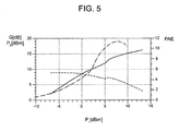
- Figure 5 shows, by way of example, the simulation of the performance as to RF power of an RF power amplifier with DDDAT structure formed according to Figures 3 and 4 using a standard 65 nm CMOS process using the applicant technology at an operating frequency of 64 GHz.
- the solid line indicates the output power PO
- the dashed line indicates the gain G
- the dashed-and-dotted line indicates the efficiency PAE as a function of the input power.
- the amplifier 30 has a high performance even at an extremely high frequency (to be compared with the frequency of 2.4 GHz achieved with the known solution described above).
- the present invention enables design and physical construction of radiofrequency power amplifiers in CMOS silicon technology, rendering them competitive as to performance and reliability as compared to more costly technologies or solutions that require increasing the number of masks for implementing complex structures or the use of sophisticated GaAs (gallium arsenide) substrates. Instead, with the present amplifier, there are no limitations to the maximum frequencies of use and thus to the potential applications.
- the represented square shape is not limiting and it is possible to adopt a variety of geometrical shapes.
- the input secondaries 36 and the output primaries 46 could be provided on a different metal level, lower or higher with respect to the input primary 35 and to the output secondary 45, respectively. They could be obtained also on metal levels different from one another.
Landscapes
- Engineering & Computer Science (AREA)
- Power Engineering (AREA)
- Amplifiers (AREA)
Claims (9)
- Leistungsverstärker (30) mit einer Vielzahl von Paaren (39) von Transistoren (40, 41), jedes Paar mit einem ersten und einem zweiten Transistor, wobei jeder einen jeweiligen Eingangsanschluss und einen jeweiligen Ausgangsanschluss aufweist; wobei die Ausgangsanschlüsse des ersten und des zweiten Transistors jedes Paars mit einem verteilten aktiven Ausgangsübertrager (32) verbunden sind, der mit einem differenziellen Ausgang (48) des Leistungsverstärkers gekoppelt ist und eine Vielzahl von Ausgangsprimärelementen (41) aufweist, welche wenigstens ein erstes und ein zweites Ausgangsprimärelement und ein Ausgangssekundärelement (45) aufweisen, wobei der Ausgangsanschluss des ersten Transistors (40) eines Paars (39) mit einem Ende des ersten Ausgangsprimärelements (46) gekoppelt ist und der Ausgangsanschluss des zweiten Transistors (41) dieses Paars mit einem Ende des zweiten Ausgangsprimärelements (46) gekoppelt ist und das Ausgangssekundärelement (45) der Vielzahl von Ausgangsprimärelementen (46) gegenüberliegt,
dadurch gekennzeichnet, dass die Eingangsanschlüsse des ersten und des zweiten Transistors jedes Paars mit einem verteilten aktiven Eingangsübertrager (31) verbunden sind, der mit einem Eingang (37) des Leistungsverstärkers gekoppelt ist, wobei der verteilte aktive Eingangsübertrager (31) ein Eingansprimärelement (35) und eine Vielzahl von Eingangssekundärelementen (36), welche wenigstens ein erstes und ein zweites Eingangssekundärelement aufweisen, benachbart zueinander aufweist und der Eingangsanschluss des ersten Transistors (40) eines Paars (39) mit einem Ende des ersten Eingangssekundärelements (36) gekoppelt ist und der Eingangsanschluss des zweiten Transistors (40) dieses Paars mit einem Ende des zweiten Eingangssekundärelements gekoppelt ist und das Eingangsprimärelement (35) der Vielzahl von Eingangssekundärelementen (36) gegenüberliegt,
wobei der verteilte aktive Eingangs- und Ausgangsübertrager (31, 32) sich entlang Seiten einer ersten und einer zweiten planaren geometrischen Figur koaxial zueinander erstrecken und die Paare (39) von Transistoren (40, 41) nahe Kanten der geometrischen Figuren gekoppelt sind. - Leistungsverstärker gemäß Anspruch 1, wobei das Eingangsprimärelement (35) die Vielzahl von Eingangssekundärelementen (36) umgibt und die Vielzahl von Ausgangsprimärelementen (46) das Ausgangssekundärelement (45) umgibt.
- Leistungsverstärker gemäß Anspruch 2, wobei das Eingangsprimärelement (35) durch eine einzelne Metallregion gebildet ist, die sich entlang des Durchmessers einer ersten planaren geometrischen Figur erstreckt, die eine an dem Eingang (37) des Leistungsverstärkers (30) durchbrochene Seite besitzt, wobei die Eingangssekundärelemente (46) durch verschiedene Metallregionen gebildet sind, die sich parallel erstrecken und jede einer jeweiligen Seite der ersten planaren geometrischen Figur gegenüberliegt.
- Leistungsverstärker gemäß Anspruch 2, wobei das Eingangsprimärelement (35) und das Ausgangssekundärelement (45) durch Metallregionen gebildet sind, die sich in einer Metallebene erstrecken, wobei der Leistungsverstärker (30) weiter eine erste Leistungsverteilungsstruktur (50), die sich in einer weiteren Metallebene erstreckt und mit dem verteilten aktiven Ausgangsübertrager (32) gekoppelt ist, und eine zweite Leistungsverteilungsstruktur (51), die sich in einer zusätzlichen Metallebene erstreckt, welche unterschiedlich zu der weiteren Metallebene ist, und mit dem verteilten aktiven Eingangsübertrager (31) gekoppelt ist, aufweist.
- Leistungsverstärker gemäß Anspruch 4, wobei die erste Leistungsverteilungsstruktur (50) mit dem verteilten aktiven Ausgangsübertrager (32) durch erste Metalldurchkontaktierungen (55) gekoppelt ist und die zweite Leistungsverteilungsstruktur (51) mit dem verteilten aktiven Eingangsübertrager (31) durch zweite Metalldurchkontaktierungen (55, 60) gekoppelt ist.
- Leistungsverstärker gemäß Anspruch 5, wobei die zweite Leistungsverteilungsstruktur (51) sich unter der ersten Leistungsverteilungsstruktur (50) erstreckt.
- Leistungsverstärker gemäß Anspruch 6, wobei wenigstens einige Metalldurchkontaktierungen (60) der zweiten Metalldurchkontaktierungen sich durch die erste Leistungsverteilungsstruktur (50) erstrecken, wobei Isolationsregionen (61) zwischen den einigen zweiten Metalldurchkontaktierungen (60) und der ersten Leistungsverteilungsstruktur (50) zwischengefügt sind.
- Leistungsverstärker gemäß einem der Ansprüche 5 bis 7, wobei die erste und die zweite Leistungsverteilungsstruktur (50, 51) eine Vielzahl von Armen (50a, 50b, 51a, 51b) aufweisen, die sich transversal zu den Seiten der ersten und zweiten geometrischen Figur erstrecken.
- Leistungsverstärker gemäß einem der Ansprüche 1 bis 8, wobei der verteilte aktive Eingangs- und Ausgangsübertrager (31, 32) in einer einzigen Metallebene gebildet sind.
Applications Claiming Priority (1)
| Application Number | Priority Date | Filing Date | Title |
|---|---|---|---|
| ITTO2008A001010A IT1392575B1 (it) | 2008-12-30 | 2008-12-30 | Amplificatore con combinatore di potenza differenziale, a trasformatore attivo distribuito |
Publications (2)
| Publication Number | Publication Date |
|---|---|
| EP2204906A1 EP2204906A1 (de) | 2010-07-07 |
| EP2204906B1 true EP2204906B1 (de) | 2012-09-05 |
Family
ID=40852531
Family Applications (1)
| Application Number | Title | Priority Date | Filing Date |
|---|---|---|---|
| EP09179210A Active EP2204906B1 (de) | 2008-12-30 | 2009-12-15 | Verteilter aktiver Transformatorverstärker mit differentiellem Leistungskombinierer |
Country Status (3)
| Country | Link |
|---|---|
| US (1) | US8049564B2 (de) |
| EP (1) | EP2204906B1 (de) |
| IT (1) | IT1392575B1 (de) |
Families Citing this family (11)
| Publication number | Priority date | Publication date | Assignee | Title |
|---|---|---|---|---|
| US8319556B2 (en) * | 2010-11-09 | 2012-11-27 | Raytheon Company | Transformer coupled distributed amplifier |
| US8502598B2 (en) * | 2011-09-30 | 2013-08-06 | Intel Corporation | Digitally-scalable transformer combining power amplifier |
| EP2770634B1 (de) | 2013-02-25 | 2018-09-19 | Telefonaktiebolaget LM Ericsson (publ) | Verteilte Leistungsverstärkerschaltung |
| US9515062B2 (en) * | 2014-12-18 | 2016-12-06 | Intel Corporation | Electronic devices and methods having a compact multi-way transformer combiner |
| US10135405B2 (en) | 2014-12-30 | 2018-11-20 | Skyworks Solutions, Inc. | Dynamic tuning of a transformer-based radio frequency power amplifier |
| ITUB20155245A1 (it) | 2015-10-23 | 2017-04-23 | St Microelectronics Srl | Amplificatore push-pull, apparecchiatura e procedimento corrispondenti |
| ITUA20163549A1 (it) * | 2016-05-18 | 2017-11-18 | St Microelectronics Srl | Trasformatore attivo, apparecchiatura e procedimento corrispondenti |
| US10181828B2 (en) | 2016-06-29 | 2019-01-15 | Skyworks Solutions, Inc. | Active cross-band isolation for a transformer-based power amplifier |
| CN110350877A (zh) * | 2019-07-26 | 2019-10-18 | 成都理工大学 | 一种高增益分布式变压器合成的功率放大器 |
| FR3099667A1 (fr) * | 2019-07-29 | 2021-02-05 | Stmicroelectronics S.R.L. | Oscillateur commandé en tension à transformateur actif distribué |
| US11716056B2 (en) | 2020-12-02 | 2023-08-01 | Texas Instruments Incorporated | Power amplifier with series transformer combiners and harmonic tuning |
Family Cites Families (3)
| Publication number | Priority date | Publication date | Assignee | Title |
|---|---|---|---|---|
| WO2002031967A2 (en) * | 2000-10-10 | 2002-04-18 | California Institute Of Technology | Distributed circular geometry power amplifier architecture |
| US7675365B2 (en) * | 2007-01-10 | 2010-03-09 | Samsung Electro-Mechanics | Systems and methods for power amplifiers with voltage boosting multi-primary transformers |
| US7746174B2 (en) * | 2008-06-12 | 2010-06-29 | Samsung Electro-Mechanics Company, Ltd. | Systems and methods for power amplifier with integrated passive device |
-
2008
- 2008-12-30 IT ITTO2008A001010A patent/IT1392575B1/it active
-
2009
- 2009-12-15 EP EP09179210A patent/EP2204906B1/de active Active
- 2009-12-28 US US12/648,163 patent/US8049564B2/en active Active
Also Published As
| Publication number | Publication date |
|---|---|
| ITTO20081010A1 (it) | 2010-06-30 |
| US8049564B2 (en) | 2011-11-01 |
| EP2204906A1 (de) | 2010-07-07 |
| IT1392575B1 (it) | 2012-03-09 |
| US20100164628A1 (en) | 2010-07-01 |
Similar Documents
| Publication | Publication Date | Title |
|---|---|---|
| EP2204906B1 (de) | Verteilter aktiver Transformatorverstärker mit differentiellem Leistungskombinierer | |
| US7675365B2 (en) | Systems and methods for power amplifiers with voltage boosting multi-primary transformers | |
| US20100019858A1 (en) | N:m transformer and impedance matching | |
| US7576607B2 (en) | Multi-segment primary and multi-turn secondary transformer for power amplifier systems | |
| EP2461335B1 (de) | Verbindungsdrahtwandler | |
| EP2458730B1 (de) | Hochfrequenzverstärker | |
| JP4933598B2 (ja) | 分布型環状電力増幅器の構造 | |
| KR101499506B1 (ko) | 트랜스포머 결합된 분산 증폭기 | |
| Park et al. | Millimeter-wave series power combining using sub-quarter-wavelength baluns | |
| US20100164645A1 (en) | Tunable Impedance Matching Circuit | |
| CN107210714A (zh) | 变换器、功率匹配网络和数字功率放大器 | |
| Ju et al. | An efficient, broadband SiGe HBT non-uniform distributed power amplifier leveraging a compact, two-section λ/4 output impedance transformer | |
| US20070069717A1 (en) | Self-shielded electronic components | |
| Hashemi | Millimeter-wave power amplifiers and transmitters | |
| US11522503B2 (en) | Transmission line transformer and amplifying circuit | |
| Park et al. | Tournament-shaped magnetically coupled power-combiner architecture for RF CMOS power amplifier | |
| JP2008263432A (ja) | 分布型電力増幅器 | |
| Khorshidian et al. | A fully-integrated 2.6 GHz stacked switching power amplifier in 45nm SOI CMOS with> 2W output power and 43.5% efficiency | |
| US20250337378A1 (en) | Power amplifier combiner | |
| US11271530B2 (en) | Transmission line transformer and amplifying circuit | |
| US7804366B2 (en) | Millimeter wave monolithic integrated circuits | |
| US10361674B2 (en) | Radio frequency delay line | |
| Palande | Necessary requirements for successful realization a 33dBM-NXP-SiGe fully balanced distributed active transformer (ring variant) at 30GHz | |
| CA2521878A1 (en) | Self shielded electronic components |
Legal Events
| Date | Code | Title | Description |
|---|---|---|---|
| PUAI | Public reference made under article 153(3) epc to a published international application that has entered the european phase |
Free format text: ORIGINAL CODE: 0009012 |
|
| AK | Designated contracting states |
Kind code of ref document: A1 Designated state(s): AT BE BG CH CY CZ DE DK EE ES FI FR GB GR HR HU IE IS IT LI LT LU LV MC MK MT NL NO PL PT RO SE SI SK SM TR |
|
| AX | Request for extension of the european patent |
Extension state: AL BA RS |
|
| 17P | Request for examination filed |
Effective date: 20101229 |
|
| 17Q | First examination report despatched |
Effective date: 20111005 |
|
| GRAP | Despatch of communication of intention to grant a patent |
Free format text: ORIGINAL CODE: EPIDOSNIGR1 |
|
| RAP1 | Party data changed (applicant data changed or rights of an application transferred) |
Owner name: STMICROELECTRONICS SRL |
|
| GRAS | Grant fee paid |
Free format text: ORIGINAL CODE: EPIDOSNIGR3 |
|
| GRAA | (expected) grant |
Free format text: ORIGINAL CODE: 0009210 |
|
| AK | Designated contracting states |
Kind code of ref document: B1 Designated state(s): AT BE BG CH CY CZ DE DK EE ES FI FR GB GR HR HU IE IS IT LI LT LU LV MC MK MT NL NO PL PT RO SE SI SK SM TR |
|
| REG | Reference to a national code |
Ref country code: GB Ref legal event code: FG4D |
|
| REG | Reference to a national code |
Ref country code: CH Ref legal event code: EP |
|
| REG | Reference to a national code |
Ref country code: AT Ref legal event code: REF Ref document number: 574505 Country of ref document: AT Kind code of ref document: T Effective date: 20120915 |
|
| REG | Reference to a national code |
Ref country code: IE Ref legal event code: FG4D |
|
| REG | Reference to a national code |
Ref country code: DE Ref legal event code: R096 Ref document number: 602009009430 Country of ref document: DE Effective date: 20121031 |
|
| REG | Reference to a national code |
Ref country code: AT Ref legal event code: MK05 Ref document number: 574505 Country of ref document: AT Kind code of ref document: T Effective date: 20120905 |
|
| REG | Reference to a national code |
Ref country code: NL Ref legal event code: VDEP Effective date: 20120905 |
|
| PG25 | Lapsed in a contracting state [announced via postgrant information from national office to epo] |
Ref country code: LT Free format text: LAPSE BECAUSE OF FAILURE TO SUBMIT A TRANSLATION OF THE DESCRIPTION OR TO PAY THE FEE WITHIN THE PRESCRIBED TIME-LIMIT Effective date: 20120905 Ref country code: NO Free format text: LAPSE BECAUSE OF FAILURE TO SUBMIT A TRANSLATION OF THE DESCRIPTION OR TO PAY THE FEE WITHIN THE PRESCRIBED TIME-LIMIT Effective date: 20121205 Ref country code: AT Free format text: LAPSE BECAUSE OF FAILURE TO SUBMIT A TRANSLATION OF THE DESCRIPTION OR TO PAY THE FEE WITHIN THE PRESCRIBED TIME-LIMIT Effective date: 20120905 Ref country code: FI Free format text: LAPSE BECAUSE OF FAILURE TO SUBMIT A TRANSLATION OF THE DESCRIPTION OR TO PAY THE FEE WITHIN THE PRESCRIBED TIME-LIMIT Effective date: 20120905 Ref country code: CY Free format text: LAPSE BECAUSE OF FAILURE TO SUBMIT A TRANSLATION OF THE DESCRIPTION OR TO PAY THE FEE WITHIN THE PRESCRIBED TIME-LIMIT Effective date: 20120905 Ref country code: HR Free format text: LAPSE BECAUSE OF FAILURE TO SUBMIT A TRANSLATION OF THE DESCRIPTION OR TO PAY THE FEE WITHIN THE PRESCRIBED TIME-LIMIT Effective date: 20120905 |
|
| REG | Reference to a national code |
Ref country code: LT Ref legal event code: MG4D Effective date: 20120905 |
|
| PG25 | Lapsed in a contracting state [announced via postgrant information from national office to epo] |
Ref country code: LV Free format text: LAPSE BECAUSE OF FAILURE TO SUBMIT A TRANSLATION OF THE DESCRIPTION OR TO PAY THE FEE WITHIN THE PRESCRIBED TIME-LIMIT Effective date: 20120905 Ref country code: SE Free format text: LAPSE BECAUSE OF FAILURE TO SUBMIT A TRANSLATION OF THE DESCRIPTION OR TO PAY THE FEE WITHIN THE PRESCRIBED TIME-LIMIT Effective date: 20120905 Ref country code: GR Free format text: LAPSE BECAUSE OF FAILURE TO SUBMIT A TRANSLATION OF THE DESCRIPTION OR TO PAY THE FEE WITHIN THE PRESCRIBED TIME-LIMIT Effective date: 20121206 Ref country code: SI Free format text: LAPSE BECAUSE OF FAILURE TO SUBMIT A TRANSLATION OF THE DESCRIPTION OR TO PAY THE FEE WITHIN THE PRESCRIBED TIME-LIMIT Effective date: 20120905 |
|
| PG25 | Lapsed in a contracting state [announced via postgrant information from national office to epo] |
Ref country code: RO Free format text: LAPSE BECAUSE OF FAILURE TO SUBMIT A TRANSLATION OF THE DESCRIPTION OR TO PAY THE FEE WITHIN THE PRESCRIBED TIME-LIMIT Effective date: 20120905 Ref country code: ES Free format text: LAPSE BECAUSE OF FAILURE TO SUBMIT A TRANSLATION OF THE DESCRIPTION OR TO PAY THE FEE WITHIN THE PRESCRIBED TIME-LIMIT Effective date: 20121216 Ref country code: CZ Free format text: LAPSE BECAUSE OF FAILURE TO SUBMIT A TRANSLATION OF THE DESCRIPTION OR TO PAY THE FEE WITHIN THE PRESCRIBED TIME-LIMIT Effective date: 20120905 Ref country code: BE Free format text: LAPSE BECAUSE OF FAILURE TO SUBMIT A TRANSLATION OF THE DESCRIPTION OR TO PAY THE FEE WITHIN THE PRESCRIBED TIME-LIMIT Effective date: 20120905 Ref country code: IS Free format text: LAPSE BECAUSE OF FAILURE TO SUBMIT A TRANSLATION OF THE DESCRIPTION OR TO PAY THE FEE WITHIN THE PRESCRIBED TIME-LIMIT Effective date: 20130105 Ref country code: NL Free format text: LAPSE BECAUSE OF FAILURE TO SUBMIT A TRANSLATION OF THE DESCRIPTION OR TO PAY THE FEE WITHIN THE PRESCRIBED TIME-LIMIT Effective date: 20120905 Ref country code: EE Free format text: LAPSE BECAUSE OF FAILURE TO SUBMIT A TRANSLATION OF THE DESCRIPTION OR TO PAY THE FEE WITHIN THE PRESCRIBED TIME-LIMIT Effective date: 20120905 |
|
| PG25 | Lapsed in a contracting state [announced via postgrant information from national office to epo] |
Ref country code: SK Free format text: LAPSE BECAUSE OF FAILURE TO SUBMIT A TRANSLATION OF THE DESCRIPTION OR TO PAY THE FEE WITHIN THE PRESCRIBED TIME-LIMIT Effective date: 20120905 Ref country code: PT Free format text: LAPSE BECAUSE OF FAILURE TO SUBMIT A TRANSLATION OF THE DESCRIPTION OR TO PAY THE FEE WITHIN THE PRESCRIBED TIME-LIMIT Effective date: 20130107 Ref country code: PL Free format text: LAPSE BECAUSE OF FAILURE TO SUBMIT A TRANSLATION OF THE DESCRIPTION OR TO PAY THE FEE WITHIN THE PRESCRIBED TIME-LIMIT Effective date: 20120905 |
|
| PLBE | No opposition filed within time limit |
Free format text: ORIGINAL CODE: 0009261 |
|
| STAA | Information on the status of an ep patent application or granted ep patent |
Free format text: STATUS: NO OPPOSITION FILED WITHIN TIME LIMIT |
|
| PG25 | Lapsed in a contracting state [announced via postgrant information from national office to epo] |
Ref country code: BG Free format text: LAPSE BECAUSE OF FAILURE TO SUBMIT A TRANSLATION OF THE DESCRIPTION OR TO PAY THE FEE WITHIN THE PRESCRIBED TIME-LIMIT Effective date: 20121205 Ref country code: DK Free format text: LAPSE BECAUSE OF FAILURE TO SUBMIT A TRANSLATION OF THE DESCRIPTION OR TO PAY THE FEE WITHIN THE PRESCRIBED TIME-LIMIT Effective date: 20120905 Ref country code: MC Free format text: LAPSE BECAUSE OF NON-PAYMENT OF DUE FEES Effective date: 20121231 |
|
| 26N | No opposition filed |
Effective date: 20130606 |
|
| PG25 | Lapsed in a contracting state [announced via postgrant information from national office to epo] |
Ref country code: IT Free format text: LAPSE BECAUSE OF FAILURE TO SUBMIT A TRANSLATION OF THE DESCRIPTION OR TO PAY THE FEE WITHIN THE PRESCRIBED TIME-LIMIT Effective date: 20120905 |
|
| REG | Reference to a national code |
Ref country code: IE Ref legal event code: MM4A |
|
| REG | Reference to a national code |
Ref country code: DE Ref legal event code: R097 Ref document number: 602009009430 Country of ref document: DE Effective date: 20130606 |
|
| PG25 | Lapsed in a contracting state [announced via postgrant information from national office to epo] |
Ref country code: IE Free format text: LAPSE BECAUSE OF NON-PAYMENT OF DUE FEES Effective date: 20121215 |
|
| PG25 | Lapsed in a contracting state [announced via postgrant information from national office to epo] |
Ref country code: MT Free format text: LAPSE BECAUSE OF FAILURE TO SUBMIT A TRANSLATION OF THE DESCRIPTION OR TO PAY THE FEE WITHIN THE PRESCRIBED TIME-LIMIT Effective date: 20120905 |
|
| PG25 | Lapsed in a contracting state [announced via postgrant information from national office to epo] |
Ref country code: TR Free format text: LAPSE BECAUSE OF FAILURE TO SUBMIT A TRANSLATION OF THE DESCRIPTION OR TO PAY THE FEE WITHIN THE PRESCRIBED TIME-LIMIT Effective date: 20120905 |
|
| PG25 | Lapsed in a contracting state [announced via postgrant information from national office to epo] |
Ref country code: SM Free format text: LAPSE BECAUSE OF FAILURE TO SUBMIT A TRANSLATION OF THE DESCRIPTION OR TO PAY THE FEE WITHIN THE PRESCRIBED TIME-LIMIT Effective date: 20120905 Ref country code: LU Free format text: LAPSE BECAUSE OF NON-PAYMENT OF DUE FEES Effective date: 20121215 |
|
| PGFP | Annual fee paid to national office [announced via postgrant information from national office to epo] |
Ref country code: FR Payment date: 20131219 Year of fee payment: 5 |
|
| PG25 | Lapsed in a contracting state [announced via postgrant information from national office to epo] |
Ref country code: HU Free format text: LAPSE BECAUSE OF FAILURE TO SUBMIT A TRANSLATION OF THE DESCRIPTION OR TO PAY THE FEE WITHIN THE PRESCRIBED TIME-LIMIT Effective date: 20091215 |
|
| REG | Reference to a national code |
Ref country code: CH Ref legal event code: PL |
|
| GBPC | Gb: european patent ceased through non-payment of renewal fee |
Effective date: 20131215 |
|
| PG25 | Lapsed in a contracting state [announced via postgrant information from national office to epo] |
Ref country code: LI Free format text: LAPSE BECAUSE OF NON-PAYMENT OF DUE FEES Effective date: 20131231 Ref country code: CH Free format text: LAPSE BECAUSE OF NON-PAYMENT OF DUE FEES Effective date: 20131231 |
|
| PG25 | Lapsed in a contracting state [announced via postgrant information from national office to epo] |
Ref country code: GB Free format text: LAPSE BECAUSE OF NON-PAYMENT OF DUE FEES Effective date: 20131215 |
|
| PG25 | Lapsed in a contracting state [announced via postgrant information from national office to epo] |
Ref country code: MK Free format text: LAPSE BECAUSE OF FAILURE TO SUBMIT A TRANSLATION OF THE DESCRIPTION OR TO PAY THE FEE WITHIN THE PRESCRIBED TIME-LIMIT Effective date: 20120905 |
|
| REG | Reference to a national code |
Ref country code: FR Ref legal event code: ST Effective date: 20150831 |
|
| PG25 | Lapsed in a contracting state [announced via postgrant information from national office to epo] |
Ref country code: FR Free format text: LAPSE BECAUSE OF NON-PAYMENT OF DUE FEES Effective date: 20141231 |
|
| REG | Reference to a national code |
Ref country code: DE Ref legal event code: R082 Ref document number: 602009009430 Country of ref document: DE Representative=s name: SCHMITT-NILSON SCHRAUD WAIBEL WOHLFROM PATENTA, DE |
|
| PGFP | Annual fee paid to national office [announced via postgrant information from national office to epo] |
Ref country code: DE Payment date: 20251126 Year of fee payment: 17 |