EP2204851A2 - Ovonic threshold switch film composition for TSLAGS material - Google Patents
Ovonic threshold switch film composition for TSLAGS material Download PDFInfo
- Publication number
- EP2204851A2 EP2204851A2 EP09180927A EP09180927A EP2204851A2 EP 2204851 A2 EP2204851 A2 EP 2204851A2 EP 09180927 A EP09180927 A EP 09180927A EP 09180927 A EP09180927 A EP 09180927A EP 2204851 A2 EP2204851 A2 EP 2204851A2
- Authority
- EP
- European Patent Office
- Prior art keywords
- threshold switch
- ovonic threshold
- alloy
- range
- state
- Prior art date
- Legal status (The legal status is an assumption and is not a legal conclusion. Google has not performed a legal analysis and makes no representation as to the accuracy of the status listed.)
- Granted
Links
- 239000000203 mixture Substances 0.000 title description 30
- 239000000463 material Substances 0.000 title description 29
- 229910045601 alloy Inorganic materials 0.000 claims abstract description 72
- 239000000956 alloy Substances 0.000 claims abstract description 72
- 150000004770 chalcogenides Chemical class 0.000 claims abstract description 39
- 230000008859 change Effects 0.000 claims description 33
- IJGRMHOSHXDMSA-UHFFFAOYSA-N Atomic nitrogen Chemical compound N#N IJGRMHOSHXDMSA-UHFFFAOYSA-N 0.000 abstract description 46
- 239000011669 selenium Substances 0.000 abstract description 28
- 229910052757 nitrogen Inorganic materials 0.000 abstract description 23
- 229910052710 silicon Inorganic materials 0.000 abstract description 22
- 239000010703 silicon Substances 0.000 abstract description 22
- BUGBHKTXTAQXES-UHFFFAOYSA-N Selenium Chemical compound [Se] BUGBHKTXTAQXES-UHFFFAOYSA-N 0.000 abstract description 20
- 229910052785 arsenic Inorganic materials 0.000 abstract description 20
- PORWMNRCUJJQNO-UHFFFAOYSA-N tellurium atom Chemical compound [Te] PORWMNRCUJJQNO-UHFFFAOYSA-N 0.000 abstract description 20
- NINIDFKCEFEMDL-UHFFFAOYSA-N Sulfur Chemical compound [S] NINIDFKCEFEMDL-UHFFFAOYSA-N 0.000 abstract description 19
- RQNWIZPPADIBDY-UHFFFAOYSA-N arsenic atom Chemical compound [As] RQNWIZPPADIBDY-UHFFFAOYSA-N 0.000 abstract description 19
- 239000011593 sulfur Substances 0.000 abstract description 19
- 229910052711 selenium Inorganic materials 0.000 abstract description 17
- 229910052714 tellurium Inorganic materials 0.000 abstract description 17
- 229910052717 sulfur Inorganic materials 0.000 abstract description 15
- 229910052732 germanium Inorganic materials 0.000 abstract description 10
- GNPVGFCGXDBREM-UHFFFAOYSA-N germanium atom Chemical compound [Ge] GNPVGFCGXDBREM-UHFFFAOYSA-N 0.000 abstract description 10
- 229910000796 S alloy Inorganic materials 0.000 abstract description 9
- 229910001370 Se alloy Inorganic materials 0.000 abstract description 4
- 229910001215 Te alloy Inorganic materials 0.000 abstract description 4
- XUIMIQQOPSSXEZ-UHFFFAOYSA-N Silicon Chemical compound [Si] XUIMIQQOPSSXEZ-UHFFFAOYSA-N 0.000 description 21
- 239000012782 phase change material Substances 0.000 description 11
- 239000010408 film Substances 0.000 description 9
- 238000000034 method Methods 0.000 description 9
- 230000008569 process Effects 0.000 description 8
- 229910017000 As2Se3 Inorganic materials 0.000 description 6
- 229910052958 orpiment Inorganic materials 0.000 description 6
- RYGMFSIKBFXOCR-UHFFFAOYSA-N Copper Chemical compound [Cu] RYGMFSIKBFXOCR-UHFFFAOYSA-N 0.000 description 5
- 239000004020 conductor Substances 0.000 description 5
- 238000001816 cooling Methods 0.000 description 5
- 229910052802 copper Inorganic materials 0.000 description 5
- 239000010949 copper Substances 0.000 description 5
- 238000010348 incorporation Methods 0.000 description 5
- VYPSYNLAJGMNEJ-UHFFFAOYSA-N Silicium dioxide Chemical compound O=[Si]=O VYPSYNLAJGMNEJ-UHFFFAOYSA-N 0.000 description 4
- 229910002056 binary alloy Inorganic materials 0.000 description 4
- 230000015556 catabolic process Effects 0.000 description 4
- 230000007423 decrease Effects 0.000 description 4
- 230000032798 delamination Effects 0.000 description 3
- 238000010438 heat treatment Methods 0.000 description 3
- 230000000737 periodic effect Effects 0.000 description 3
- 229920002120 photoresistant polymer Polymers 0.000 description 3
- 229910002059 quaternary alloy Inorganic materials 0.000 description 3
- 229910000967 As alloy Inorganic materials 0.000 description 2
- 229910000618 GeSbTe Inorganic materials 0.000 description 2
- 230000004888 barrier function Effects 0.000 description 2
- 238000005229 chemical vapour deposition Methods 0.000 description 2
- 238000000280 densification Methods 0.000 description 2
- 238000000151 deposition Methods 0.000 description 2
- 230000008021 deposition Effects 0.000 description 2
- 229910021476 group 6 element Inorganic materials 0.000 description 2
- 239000012535 impurity Substances 0.000 description 2
- 230000010354 integration Effects 0.000 description 2
- 238000004519 manufacturing process Methods 0.000 description 2
- 229910052751 metal Inorganic materials 0.000 description 2
- 239000002184 metal Substances 0.000 description 2
- 239000011148 porous material Substances 0.000 description 2
- 238000012545 processing Methods 0.000 description 2
- 230000000717 retained effect Effects 0.000 description 2
- 239000004065 semiconductor Substances 0.000 description 2
- 235000012239 silicon dioxide Nutrition 0.000 description 2
- 239000000377 silicon dioxide Substances 0.000 description 2
- 238000001228 spectrum Methods 0.000 description 2
- 239000000758 substrate Substances 0.000 description 2
- KRHYYFGTRYWZRS-UHFFFAOYSA-N Fluorane Chemical compound F KRHYYFGTRYWZRS-UHFFFAOYSA-N 0.000 description 1
- KJTLSVCANCCWHF-UHFFFAOYSA-N Ruthenium Chemical compound [Ru] KJTLSVCANCCWHF-UHFFFAOYSA-N 0.000 description 1
- RTAQQCXQSZGOHL-UHFFFAOYSA-N Titanium Chemical compound [Ti] RTAQQCXQSZGOHL-UHFFFAOYSA-N 0.000 description 1
- NRTOMJZYCJJWKI-UHFFFAOYSA-N Titanium nitride Chemical compound [Ti]#N NRTOMJZYCJJWKI-UHFFFAOYSA-N 0.000 description 1
- 238000009825 accumulation Methods 0.000 description 1
- 238000003491 array Methods 0.000 description 1
- 230000006399 behavior Effects 0.000 description 1
- 230000015572 biosynthetic process Effects 0.000 description 1
- 230000001413 cellular effect Effects 0.000 description 1
- 229910017052 cobalt Inorganic materials 0.000 description 1
- 239000010941 cobalt Substances 0.000 description 1
- GUTLYIVDDKVIGB-UHFFFAOYSA-N cobalt atom Chemical compound [Co] GUTLYIVDDKVIGB-UHFFFAOYSA-N 0.000 description 1
- 238000004891 communication Methods 0.000 description 1
- 239000000470 constituent Substances 0.000 description 1
- 238000002425 crystallisation Methods 0.000 description 1
- 230000008025 crystallization Effects 0.000 description 1
- 238000010586 diagram Methods 0.000 description 1
- 238000009792 diffusion process Methods 0.000 description 1
- 238000005516 engineering process Methods 0.000 description 1
- 229910000040 hydrogen fluoride Inorganic materials 0.000 description 1
- 238000003384 imaging method Methods 0.000 description 1
- 229910003437 indium oxide Inorganic materials 0.000 description 1
- PJXISJQVUVHSOJ-UHFFFAOYSA-N indium(iii) oxide Chemical compound [O-2].[O-2].[O-2].[In+3].[In+3] PJXISJQVUVHSOJ-UHFFFAOYSA-N 0.000 description 1
- 239000011810 insulating material Substances 0.000 description 1
- 238000005259 measurement Methods 0.000 description 1
- 230000003287 optical effect Effects 0.000 description 1
- 238000005240 physical vapour deposition Methods 0.000 description 1
- 229910021420 polycrystalline silicon Inorganic materials 0.000 description 1
- 238000005546 reactive sputtering Methods 0.000 description 1
- 230000009467 reduction Effects 0.000 description 1
- 230000002441 reversible effect Effects 0.000 description 1
- 238000012552 review Methods 0.000 description 1
- 229910052707 ruthenium Inorganic materials 0.000 description 1
- 239000000523 sample Substances 0.000 description 1
- HBMJWWWQQXIZIP-UHFFFAOYSA-N silicon carbide Chemical compound [Si+]#[C-] HBMJWWWQQXIZIP-UHFFFAOYSA-N 0.000 description 1
- 229910010271 silicon carbide Inorganic materials 0.000 description 1
- 238000004544 sputter deposition Methods 0.000 description 1
- 230000003068 static effect Effects 0.000 description 1
- 239000000126 substance Substances 0.000 description 1
- 229910052715 tantalum Inorganic materials 0.000 description 1
- GUVRBAGPIYLISA-UHFFFAOYSA-N tantalum atom Chemical compound [Ta] GUVRBAGPIYLISA-UHFFFAOYSA-N 0.000 description 1
- MZLGASXMSKOWSE-UHFFFAOYSA-N tantalum nitride Chemical compound [Ta]#N MZLGASXMSKOWSE-UHFFFAOYSA-N 0.000 description 1
- 238000007736 thin film deposition technique Methods 0.000 description 1
- 239000010936 titanium Substances 0.000 description 1
- 229910052719 titanium Inorganic materials 0.000 description 1
- MAKDTFFYCIMFQP-UHFFFAOYSA-N titanium tungsten Chemical compound [Ti].[W] MAKDTFFYCIMFQP-UHFFFAOYSA-N 0.000 description 1
- 230000009466 transformation Effects 0.000 description 1
- 238000000844 transformation Methods 0.000 description 1
- 230000001960 triggered effect Effects 0.000 description 1
- 229910052721 tungsten Inorganic materials 0.000 description 1
- 239000010937 tungsten Substances 0.000 description 1
- -1 tungsten nitride Chemical class 0.000 description 1
Images


Classifications
-
- H—ELECTRICITY
- H10—SEMICONDUCTOR DEVICES; ELECTRIC SOLID-STATE DEVICES NOT OTHERWISE PROVIDED FOR
- H10N—ELECTRIC SOLID-STATE DEVICES NOT OTHERWISE PROVIDED FOR
- H10N70/00—Solid-state devices without a potential-jump barrier or surface barrier, and specially adapted for rectifying, amplifying, oscillating or switching
- H10N70/801—Constructional details of multistable switching devices
- H10N70/881—Switching materials
- H10N70/882—Compounds of sulfur, selenium or tellurium, e.g. chalcogenides
-
- C—CHEMISTRY; METALLURGY
- C01—INORGANIC CHEMISTRY
- C01B—NON-METALLIC ELEMENTS; COMPOUNDS THEREOF; METALLOIDS OR COMPOUNDS THEREOF NOT COVERED BY SUBCLASS C01C
- C01B19/00—Selenium; Tellurium; Compounds thereof
- C01B19/002—Compounds containing, besides selenium or tellurium, more than one other element, with -O- and -OH not being considered as anions
-
- H—ELECTRICITY
- H10—SEMICONDUCTOR DEVICES; ELECTRIC SOLID-STATE DEVICES NOT OTHERWISE PROVIDED FOR
- H10B—ELECTRONIC MEMORY DEVICES
- H10B63/00—Resistance change memory devices, e.g. resistive RAM [ReRAM] devices
- H10B63/20—Resistance change memory devices, e.g. resistive RAM [ReRAM] devices comprising selection components having two electrodes, e.g. diodes
- H10B63/24—Resistance change memory devices, e.g. resistive RAM [ReRAM] devices comprising selection components having two electrodes, e.g. diodes of the Ovonic threshold switching type
-
- H—ELECTRICITY
- H10—SEMICONDUCTOR DEVICES; ELECTRIC SOLID-STATE DEVICES NOT OTHERWISE PROVIDED FOR
- H10N—ELECTRIC SOLID-STATE DEVICES NOT OTHERWISE PROVIDED FOR
- H10N70/00—Solid-state devices without a potential-jump barrier or surface barrier, and specially adapted for rectifying, amplifying, oscillating or switching
- H10N70/011—Manufacture or treatment of multistable switching devices
- H10N70/021—Formation of the switching material, e.g. layer deposition
- H10N70/026—Formation of the switching material, e.g. layer deposition by physical vapor deposition, e.g. sputtering
-
- H—ELECTRICITY
- H10—SEMICONDUCTOR DEVICES; ELECTRIC SOLID-STATE DEVICES NOT OTHERWISE PROVIDED FOR
- H10N—ELECTRIC SOLID-STATE DEVICES NOT OTHERWISE PROVIDED FOR
- H10N70/00—Solid-state devices without a potential-jump barrier or surface barrier, and specially adapted for rectifying, amplifying, oscillating or switching
- H10N70/011—Manufacture or treatment of multistable switching devices
- H10N70/041—Modification of the switching material, e.g. post-treatment, doping
-
- H—ELECTRICITY
- H10—SEMICONDUCTOR DEVICES; ELECTRIC SOLID-STATE DEVICES NOT OTHERWISE PROVIDED FOR
- H10N—ELECTRIC SOLID-STATE DEVICES NOT OTHERWISE PROVIDED FOR
- H10N70/00—Solid-state devices without a potential-jump barrier or surface barrier, and specially adapted for rectifying, amplifying, oscillating or switching
- H10N70/20—Multistable switching devices, e.g. memristors
-
- H—ELECTRICITY
- H10—SEMICONDUCTOR DEVICES; ELECTRIC SOLID-STATE DEVICES NOT OTHERWISE PROVIDED FOR
- H10N—ELECTRIC SOLID-STATE DEVICES NOT OTHERWISE PROVIDED FOR
- H10N70/00—Solid-state devices without a potential-jump barrier or surface barrier, and specially adapted for rectifying, amplifying, oscillating or switching
- H10N70/801—Constructional details of multistable switching devices
- H10N70/821—Device geometry
- H10N70/826—Device geometry adapted for essentially vertical current flow, e.g. sandwich or pillar type devices
-
- C—CHEMISTRY; METALLURGY
- C01—INORGANIC CHEMISTRY
- C01P—INDEXING SCHEME RELATING TO STRUCTURAL AND PHYSICAL ASPECTS OF SOLID INORGANIC COMPOUNDS
- C01P2006/00—Physical properties of inorganic compounds
- C01P2006/40—Electric properties
Definitions
- the present disclosure relates generally to compositions of ovonic threshold switches.
- a phase change memory device includes an array of memory cells, where each memory cell includes a memory element and a selection element.
- the memory element is a phase change material, i . e ., a chalcogenide alloy that may be electrically switched between a generally amorphous and a generally crystalline state or between different detectable states of local order across the entire spectrum between completely amorphous and completely crystalline states.
- the state of the phase change material is also non-volatile in that, when set in a crystalline, semi-crystalline, amorphous, or semi-amorphous state representing a resistance value, that value is retained until changed by another programming event.
- the resistance value that is retained represents a phase or physical state of the material ( e . g ., crystalline or amorphous). This physical state of the phase change material is unaffected by removing electrical power.
- the selection element may also be made of a chalcogenide alloy, however, unlike the memory element, the selection element does not change phase. More particularly, the selection element, which may be referred to throughout as an ovonic threshold switch, an OTS, or a switching device, does not exhibit a phase change from amorphous to crystalline.
- An ovonic threshold switch toggles between an "on” and “off” state depending on the amount of voltage potential applied across the phase change memory cell. The state of the ovonic threshold switch changes when a current through the ovonic threshold switch exceeds a threshold current or voltage. Once the threshold current or voltage is reached, the on state is triggered and the ovonic threshold switch is in a substantially conductive state. If the current or voltage potential drops below a threshold value, the ovonic threshold switch will return to the off state.
- references also describe the structural transformations from the crystalline state to the amorphous state (and vice versa), including a series of partially crystalline states in which the relative proportions of crystalline and amorphous regions may vary during the operation of electrical and optical chalcogenide materials.
- the phase change material is typically formed with one or more chalcogenide elements (i . e ., Group VI elements from the periodic table).
- chalcogenide elements i . e ., Group VI elements from the periodic table.
- Examples of chalcogenide materials are described in U.S. Patent Nos. 5,166,758 , 5,296,716 , 5,414,271 , 5,359,205 , 5,341,328 , 5,536,947 , 5,534,712 , 5,687,112 , and 5,825,046 the disclosures of which are all incorporated by reference herein.
- the present disclosure is directed to alternative chalcogenide alloy compositions that optimize the performance characteristics of chalcogenic switching devices, such as ovonic threshold switches.
- chalcogenide alloy an ovonic threshold switch, a phase change memory cell and a memory, according to claims 1, 7, 13 and 14, respectively.
- the present chalcogenide alloy for an ovonic threshold switch can sustain high field strengths and provide low off state leakage with stable threshold voltages, V TH .
- Embodiments in accordance with the principles of the present disclosure may include binary, ternary, quaternary, and higher order chalcogenide alloys.
- a chalcogenide alloy that optimizes operating parameters of an ovonic threshold switch includes arsenic at an atomic percentage in the range of 9 to 39, germanium at an atomic percentage in the range of 10 and 40, silicon at an atomic percentage in the range of 5 and 18, nitrogen at an atomic percentage in the range of 0 and 10, and an alloy of sulfur, selenium, and tellurium.
- a ratio of sulfur to selenium in the range of 0.25 and 4 and a ratio of sulfur to tellurium in the alloy of sulfur, selenium, and tellurium is in the range of 0.11 and 1.
- a chalcogenide includes the composition As m X q Ge r Si t N z , where m is an atomic percentage of the alloy in the range of 9 to 39, q is an atomic percentage of the alloy in the range of 17 and 60, r is an atomic percentage of the alloy in the range of 10 and 40, t is an atomic percentage of the alloy in the range of 5 and 18, and z is an atomic percentage of the alloy in the range of 0 and 10.
- the chalcogenide alloy also includes X is S a Se d Te g where a/d is in the range of 0.25 and 4 and a/g is in the range of 0.11 and 1.
- ovonic threshold switch that is a chalcogenide alloy having the formula described herein.
- a phase change memory cell that includes a phase change memory layer and an ovonic threshold switch layer formed of a chalcogenide alloy having the composition described herein.
- a memory is also provided that includes a wordline, a bitline, a phase change memory layer, a first electrode that separates the phase change memory layer from the wordline, and an ovonic threshold switch layer formed of a chalcogenide alloy described herein.
- alloy components described herein theoretically add up to an atomic percentage of 100, but the compositional ranges are determined by empirical formula.
- a memory array 100 includes a plurality of memory cells 102 positioned between a plurality of bit lines 104 and word lines 106.
- Each memory cell 102 includes an ovonic threshold switch 108 and a memory element 110.
- Both the ovonic threshold switch 108 and the memory element 110 may be formed of a chalcogenide composition, an alloy of elements of group VI of the periodic table, such as Te, S, or Se.
- the memory element 110 may be a phase change material that switches from a high resistance state, generally amorphous, to a low resistance state, generally crystalline, upon the application of energy such as heat, light, voltage potential, or electrical current.
- the phase change material may be switched from completely amorphous to completely crystalline or between different detectable states of local order across the entire spectrum between completely amorphous and completely crystalline.
- Programming the phase change material to alter its state or phase may be accomplished by applying voltage potentials across electrodes, thereby generating a voltage potential across the ovonic threshold switch 108 and the memory element 110.
- V TH threshold voltage
- an electrical current may flow through the ovonic threshold switch 108 and the phase change material in the memory element 110 and may result in heating of the phase change material. This heating may alter the memory state or phase of the phase change material, thus altering the electrical characteristic of the memory element 110, e . g ., the resistance.
- the memory material may also be referred to as a programmable resistance material.
- the amorphous or semi-amorphous state may be associated with a "reset” state or a logic “0" value, while a crystalline or semi-crystalline state may be associated with a "set” state, or a logic “1” value.
- the resistance of memory material in the amorphous or semi-amorphous state is generally greater than the resistance of memory material in the crystalline or semi-crystalline state. It is to be appreciated that the association of reset and set with amorphous and crystalline states, respectively, is a convention and that at least an opposite convention may be adopted.
- the phase change memory material may be heated to a relatively higher temperature to amorphize memory material and "reset” memory material (e . g ., program memory material to "0"). Heating the volume of memory material to a relatively lower crystallization temperature may crystallize memory material and "set” memory material ( e . g ., program memory material to "1 ").
- Various resistances of memory material may be achieved to store information by varying the amount of current flow and duration through the volume of memory material.
- the memory elements 110 of the memory cells 102 may be connected to the word lines 106 and to the bit lines 104 through the ovonic threshold switch 108. To select a particular memory cell 102, voltage potentials may be applied across the associated bit line 104 and word line 106.
- the ovonic threshold switch 108 may be used to access the memory element 110 during programming or reading operations.
- the chalcogenide material in the ovonic threshold switch 108 does not change state or phase upon the application of energy. Instead, the switching material used in the ovonic threshold switch 108 may be in a substantially amorphous state that may be repeatedly and reversibly switched between a higher resistance "off" state and a lower resistance "on” state.
- the ovonic threshold switch 108 is either on or off depending on the amount of voltage potential applied across the memory cell 102.
- the off state may be substantially non conductive and the on state may be substantially conductive.
- the ovonic threshold switch 108 is formed of a chalcogenide alloy that provides reproducible switching at fast switching speeds.
- Basic principles and operational features of ovonic threshold switches are presented, for example, in U.S. Patent Nos. 3,271,591 ; 5,543,737 ; 5,694,146 ; and 5,757,446 ; the disclosures of which are hereby incorporated by reference, as well as in several journal articles including Ovshinsky, S.R., "Reversible Electrical Switching Phenomena in Disordered Structures," Physical Review Letters 21:1450-1453 (1969 ); Ovshinsky, S.R. and Fritzsche, H.
- the ovonic threshold switch 108 switches between the off and the on state by applying an electrical current or voltage potential that exceeds a threshold current or threshold voltage, I TH and V TH , respectively. If a voltage potential is less than V TH of the ovonic threshold switch 108, then the ovonic threshold switch 108 remains in the off or highly resistive state. Little or no electrical current passes through the memory cell 102 when the ovonic threshold switch 108 is in the off state. If a voltage potential greater than V TH is applied, then the ovonic threshold switch 108 may switch to the on state and operate in a relatively low resistive state. In the on state, current passes through the memory cell 102 and can be used to read or program the memory element 110.
- I TH and V TH a threshold current or threshold voltage
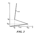
- Figure 2 illustrates an example I-V characteristic of the switching material in ovonic threshold switch 108. Since the switching material of the ovonic threshold switch 108 may remain in an amorphous state, the current-voltage (I-V) characteristic may remain the same throughout the operating life of the ovonic threshold switch 108.
- I-V current-voltage
- the ovonic threshold switch 108 When the voltage across the ovonic threshold switch 108 is less than the threshold voltage, V TH , the ovonic threshold switch 108 is in a substantially nonconductive state, i . e ., an off state curve 112. If a voltage potential greater than V TH or a current greater than I TH is applied, then the ovonic threshold switch 108 turns on, i . e ., an on state curve 114. If the voltage potential across the ovonic threshold switch 108 is greater than V TH , then the voltage potential across the ovonic threshold switch 108 may drop or snapback to a holding voltage potential, V H .
- the voltage potential across the ovonic threshold switch 108 may remain close to V H , see the on state curve 114.
- the ovonic threshold switch 108 may remain in the on state until the current decreases to below a holding current I H . Once the current falls below I H , the ovonic threshold switch 108 may turn off and return to the highly resistive state. In order to switch the ovonic threshold switch 108 back to the on state, a voltage greater than or equal to the threshold voltage must be applied across the ovonic threshold switch 108.
- the current across the ovonic threshold switch 108 increases only a small amount as the voltage potential is increased.
- the switching material instantaneously switches from the off state to the on state, which is illustrated by the dashed line.
- the voltage through the ovonic threshold switch 108 decreases significantly to the holding voltage, V H .
- the curve of the on state 114 has a steeper slope than the off state curve 112.
- the present disclosure is directed to an ovonic threshold switch film composition that can sustain high field strength and provide low off state leakage with stable threshold voltages, V TH .
- the ovonic threshold switch 108 is a chalcogenide alloy that includes tellurium, sulfur, arsenic, germanium, and selenium, which will be referred to as TSLAGS.
- the TSLAGS ovonic threshold switch 108 composition also includes silicon and may be formed with or without nitrogen.
- the TSLAGS composition for the ovonic threshold switch 108 may be formed by combining several alloys together.
- the TSLAGS composition may be started by first forming a number of binary alloys. More specifically, an alloy of arsenic and sulfur can be prepared that has proportions ranging from 30% to 45% and from 55% to 70%, respectively.
- another alloy may be formed that includes arsenic and selenium having proportions ranging from 30% to 45% and from 55% to 70%, respectively.
- An additional alloy may be formed that includes arsenic and tellurium combined having proportions ranging from 30% to 45% and from 55% to 70%, respectively.
- these binary chalcogenide alloys of arsenic/sulfur, arsenic/selenium, and arsenic/tellurium are As 2 S 3 , As 2 Se 3 , and As 2 Te 3 , respectively.
- a quaternary alloy comprising arsenic, sulfur, selenium, and tellurium may be formed.
- the binary alloys of arsenic/sulfur, arsenic/selenium, and arsenic/tellurium can be combined to form a single alloy of As, Se, S, Te, in which the element-pair sulfur/selenium have proportions ranging from 20% to 80% and from 20% to 80%, respectively.
- the element-pair of sulfur/tellurium have proportions ranging from 10% to 50%, and from 50% to 90%, respectively
- the element-pair of selenium/tellurium have proportions ranging from 10% to 50% and from 50% to 90%, respectively.
- quaternary alloys of arsenic/sulfur/selenium/tellurium may also be formed according to the previously described proportions. More particularly, sulfur, selenium, and tellurium are interchangeable so that the proportions of these three elements to each other may be varied with in the parameters discussed above with respect to tertiary combinations with the binary alloys arsenic/sulfur, arsenic/selenium, and arsenic/tellurium.
- the elements sulfur, selenium, and tellurium may be used interchangeably in the percentages described above since these elements form similar crystalline structures and arrange in the same lattice positions.
- germanium may be added in the range of 10% to 40% and silicon may be added in the range of 5% to 18%.
- Germanium and silicon may be incorporated in various ways, such as composite-target incorporation, cosputtering, and metal organic chemical vapor deposition (MOCVD). The incorporation of silicon provides compatibility with high-temperature integrated circuit back-end fabrication processing.
- nitrogen, N 2 may be added to the TSLAGS ovonic threshold switch alloys above in the range of 0% to 10% to enhance the ovonic threshold switch 108 characteristics. Nitrogen may be incorporated through reactive sputtering, composite-target incorporation, or other suitable processes.
- This TSLAGS ovonic threshold switch composition having silicon with or without the inclusion of nitrogen balances the key functional requirements and minimizes off-state leakage and sub-threshold I-V swing, variation of the threshold voltage over many cycles, drift of the threshold voltage with delay time between pulses, and optimizes cycle life and operating current densities.
- the TSLAGS composition provides high thermal robustness needed for integration into back-end fab-processing.
- Breakdown field strengths are the major intrinsic property that relates to the threshold voltage needed for switching of ovonic threshold switches.
- different ovonic threshold switch compositions have different breakdown field strengths.
- Traditional binary chalcogenide alloys, such as As 2 S 3 and As 2 Se 3 have relatively high field strengths, between 1x10 6 and 1x10 7 volts/centimeter. Strong field strength alloys, such as As 2 S 3 and As 2 Se 3 , require less film thickness to be deposited than weak field strength alloys, in order to achieve a given threshold voltage target.
- Other binary chalcogenide alloys, such as As 2 Te 3 have relatively low field strengths, between 1x10 5 and 1x10 6 volts/centimeter. Therefore As 2 Te 3 alloys require thicker films to achieve desired threshold voltages.
- the TSLAGS ovonic threshold switch composition with nitrogen and silicon can achieve a threshold voltage, V TH , of 4.5V at a film thickness of 600 Angstroms.
- V TH threshold voltage
- the breakdown field strength of this TSLAGS composition is not as high as the As 2 S 3 and As 2 Se 3 alloys and not as low as the As 2 Te 3 alloys. Therefore, the TSLAGS composition does not require a film thickness as large as the alloy, As 2 Te 3 .
- Chalcogenide alloys must be thermally robust in order to be feasibly integrated into a semiconductor process sequence, due to high-temperature steps that occur during back-end steps of device fabrication. It is advantageous to maximize the temperature an alloy can withstand before sublimating into the surrounding space, delaminating from adjacent film layers, or otherwise forfeiting its desired electrical properties.
- An alloy should be able to withstand temperatures of at least 300-350 degrees Celsius for integration into most existing process technologies.
- the alloy, As 2 S 3 has the lowest thermal robustness at around 150 degrees Celsius.
- the alloys As 2 Te 3 and As 2 Se 3 yield a thermal robustness rating less than 300 degrees Celsius.
- a higher proportion of germanium in the whole chalcogenide alloy results in improved thermal robustness. For example, incorporating 40% germanium results in significantly less delamination after an anneal at 350 degrees Celsius than 10% germanium.
- the TSLAGS composition with nitrogen and silicon also achieves a desirable thermal robustness of approximately 350 degrees Celsius.
- a higher proportion of silicon also improves the thermal robustness of the chalcogenide alloy. For example, incorporating 10% silicon into the whole alloy reduces occurrence of delaminations during an anneal at 350 degrees Celsius, as compared to only 5% silicon.
- the off-state leakage current Another parameter that is optimized by the TSLAGS ovonic threshold switch material having silicon and formed with or without nitrogen is the off-state leakage current.
- the off-state leakage current is strongly related to the alloy's field strength, i . e ., the higher the field strength the lower the off-state leakage current.
- Incorporation of nitrogen reduces the off-state leakage current of the alloy. For example, an inclusion of 2% nitrogen can decrease the off-state leakage current.
- introduction of nitrogen also improves the thermal robustness of the ovonic threshold switch.
- a higher proportion of nitrogen such as 4%, reduces the occurrence of delamination at an anneal of 350 degrees Celsius, as compared to 2% nitrogen.
- the TSLAGS composition optimizes ovonic threshold switch performance by having a desirable field strength and therefore a lower off-state leakage current.
- the TSLAGS composition with nitrogen and silicon satisfies the leakage requirements for this application and achieves the desired thermal robustness specifications.
- V TH threshold voltage
- a V TH -bounce of 0.3 Volts is considered the highest-acceptable amount of variation.
- high field strength alloys such as As 2 S 3 have a high V TH - bounce, while lower field strength alloys, such as As 2 Te 3 tend to have less V TH -bounce.
- the TSLAGS composition with nitrogen and silicon achieve the desired off-state leakage current while having an acceptable V TH -bounce of approximately 0.3 Volts.
- the measurement for V TH -bounce was performed by applying 30 consecutive square pluses of 500ns width and capturing the V TH -bounce with an oscilloscope.
- a phase change memory cell 302 includes a phase change layer 310 and a TSLAGS ovonic threshold switch 308 having silicon formed with or without nitrogen.
- the ovonic threshold switch 308 is positioned between a top and a bottom electrode, 312 and 314, respectively.
- a middle electrode 316 is located between the phase change layer 310 and the ovonic threshold switch 308.
- the top electrode 312 is aligned with a bitline 304 and separates the bitline 304 from the ovonic threshold switch 308.
- the phase change layer 310 is in direct contact with the bottom electrode 314, which is in direct contact with a wordline 306.
- the phase change layer 310 is typically formed with one or more chalcogenide elements (i . e ., Group VI elements from the periodic table), as described above.
- chalcogenide elements i . e ., Group VI elements from the periodic table
- One common chalcogenide combination is GST (germanium - Antimony- tellurium).
- GST germanium - Antimony- tellurium
- any known suitable phase change material may be used.
- the bitline and wordline layers 304, 306 can be of any conductive material, and are copper in one embodiment.
- the top and bottom electrode layers 312, 314 also can be of any conductive material. If the bitline and wordline layers 304, 306 are copper, then the top and bottom electrode layers 312, 314 preferably are copper barrier materials to prevent diffusion of the copper into the ovonic threshold switch layer 308.
- copper barrier materials that can be employed include cobalt, ruthenium, tantalum, tantalum nitride, indium oxide, tungsten nitride, titanium, titanium tungsten, titanium nitride, silicon carbide, polycrystalline silicon, or other suitable conductors or resistive conductors compatible with ovonic threshold switch 308.
- Programming of the phase change memory cell 302 occurs by pulses of current applied between the bitline 304 and the wordline 306.
- the programming current rises from zero to the "reset” current value and holds the “reset” current value for up to 100ns to melt the phase change layer 310.
- the current pulse decreases to 50%-80% of the "reset” current value for 10-100 ns before returning to zero. The reduction in the programming current to 50-80% of the reset current value ensures that the ovonic threshold switch layers 308 remains in the on state, i . e . conductive while the phase change layer 310 begins cooling.
- the step down in programming current more effectively quenches the phase change layer 310 to a vitreous (amorphous) state by removing the heat in the phase change layer 310 through the highly conductive ovonic threshold switch 308 to the thermal sinks of the bitline 304 and wordline 306.
- the cooling stage determines if the phase change layer 310 solidifies in a high or low resistive state. A faster cooling process arranges the phase change layer 310 in the high resistance state, the "reset” state. A slower cooling process arranges the phase change layer 310 in the low resistance state, the "set” state.
- an ovonic threshold switch 400 may be formed as illustrated in Figure 7 .
- a first oxide layer 420 may be deposited or grown on a substrate 418, which may be a silicon wafer.
- the first oxide layer 420 may be silicon dioxide or any other suitable insulating material.
- the first oxide layer 420 is 4000 Angstroms thick (400 nanometers).
- a bottom electrode layer 414 is deposited over the first oxide layer 420 and may have a thickness of 500 Angstroms (50 nanometers).
- the bottom electrode layer 414 is 397 Angstroms (39.7 nanometers) in thickness.
- the bottom electrode 414 may be formed of any suitable conductive material as described above.
- a second oxide layer 422 may be deposited over the bottom electrode layer 414.
- the second oxide layer 422 may also be a silicon dioxide or other suitable insulating layer.
- the layers on the substrate 418 may then be subjected to a densification process at 525 degrees Celsius for one minute.
- a photoresist layer (not shown) may be deposited over the bottom electrode layer 414 to define a pore or via region 424.
- a top surface 415 of the bottom electrode 414 is exposed by the via region 424.
- the via region 424 is defined by sidewalls 417.
- the photoresist layer may be removed after the via region 424 is formed.
- a dilute hydrogen fluoride pore clean may be used to prepare the second oxide layer 422 for deposition of an ovonic threshold switch layer 408.
- the ovonic threshold switch layer 408 is a deposition of a TSLAGS composition having silicon with or without nitrogen according to an embodiment the present disclosure.
- the ovonic threshold switch layer 408 may be formed by sputter deposition with reactive nitrogen to a thickness of 675 Angstroms (67.5 nanometers).
- the TSLAGS ovonic threshold switch film may be formed using other thin film deposition techniques such as, chemical vapor deposition or physical vapor deposition.
- the ovonic threshold switch layer 408 includes 8% silicon and has a thickness of 679 Angstroms.
- the ovonic threshold switch layer 408 conforms to the sidewalls 417 of the via 424 and the top surface 415 of the bottom electrode 414.
- the ovonic threshold switch layer 408 may directly contact the bottom electrode 414 on the top surface 415.
- a top electrode 412 is deposited over the ovonic threshold switch layer 408 and may be 406 Angstroms in thickness.
- a probe pad metal layer 426 may be deposited over the top electrode 412 and in the via 424. Photoresist layers and etch steps may be used to define active areas and to define contact pads.
- the ovonic threshold switch 400 may then be heated in a convection oven anneal process at 350°C for thirty minutes. It should be noted that this is an exemplary embodiment and other suitable methods may be used to form the ovonic threshold switch 400.
- System 500 may be used in wireless devices such as a personal digital assistant, a laptop or portable computer with wireless capability, a web tablet, a wireless telephone, a pager, an instant messaging device, a digital music player, a digital camera, or other devices that may be adapted to transmit and/or receive information wirelessly.
- the system 500 may be used in any of the following systems: a wireless local area network (WLAN) system, a wireless personal area network (WPAN) system, or a cellular network, although the scope of the present invention is not limited in this respect.
- WLAN wireless local area network
- WPAN wireless personal area network
- cellular network although the scope of the present invention is not limited in this respect.
- the system 500 may include a controller 510, an input/output (I/O) device 520 ( e . g ., a keypad, display), static random access memory (SRAM) 460, a memory 530, and a wireless interface 540 coupled to each other via a bus 550.
- I/O input/output
- SRAM static random access memory
- a battery 480 may be used in some embodiments. It should be noted that the scope of the present invention is not limited to embodiments having any or all of these components.
- the controller 510 may comprise, for example, one or more microprocessors, digital signal processors, microcontrollers, or the like.
- the memory 530 may be used to store messages transmitted to or by system 500.
- the memory 530 may also optionally be used to store instructions that are executed by controller 510 during the operation of system 500, and may be used to store user data.
- the memory 530 may be provided by one or more different types of memory.
- memory 530 may comprise any type of random access memory, a volatile memory, a non-volatile memory such as a flash memory and/or a memory discussed herein.
- I/O device 520 may be used by a user to generate a message.
- the system 500 may use wireless interface 540 to transmit and receive messages to and from a wireless communication network with a radio frequency (RF) signal.
- wireless interface 540 may include an antenna or a wireless transceiver, although the scope of the present invention is not limited in this respect.
- TSLAGS material having nitrogen and 8% silicon formed as a 500 Angstrom thick film with a 150nm diameter achieved an average threshold voltage of 3.29 Volts, an average holding voltage of 1.02 Volts, an average voltage snapback of 1.90, and a current snapback of 0.39 milliamperes.
- the TSLAGS composition with silicon and nitrogen may comprise an arsenic concentration in the range of 9-39%, a germanium concentration in the range of 10-40%, a silicon concentration in the range of 5-18%, a nitrogen concentration in the range of 0-10%, and a combination of selenium, sulfur, and tellurium in a concentration in the range of 17-60%.
- the ratio of sulfur to selenium is in the range of 0.25 and 4 and the ratio of sulfur to tellurium is in the range of 0.11 and 1.
- the percentages are atomic percentages which total 100% of the atoms of the constituent elements.
- the ovonic threshold switch 108 is a chalcogenide composition of AS 25-27 S 5-6 Se 12-13 Te 28-30 Ge 17-19 Si 7-10 N 0-5 .
- the ovonic threshold switch 108 may be As 25 S 5.5 Se 12.2 Te 28.1 Ge 17.8 Si 7.1 N 4.1 , As 26.17 S 5.78 Se 12.75 Te 29.38 Ge 18.56 Si 7.37 , As 25.4 S 5.6 Se 12.3 Te 28.6 Ge 18.1 Si 9.6 , and As 25.53 S 5.6 Se 12.37 Te 28.69 Ge 18.18 Si 9.64 .
- impurities may be incorporated into any of the alloys during formation. For example, in the alloy composition As 25 S 5.5 Se 12.2 Te 28.1 Ge 17.8 Si 7.1 N 4.1 , 0.4% of the total composition is an impurity.
Abstract
Description
- The present disclosure relates generally to compositions of ovonic threshold switches.
- A phase change memory device includes an array of memory cells, where each memory cell includes a memory element and a selection element. The memory element is a phase change material, i.e., a chalcogenide alloy that may be electrically switched between a generally amorphous and a generally crystalline state or between different detectable states of local order across the entire spectrum between completely amorphous and completely crystalline states. The state of the phase change material is also non-volatile in that, when set in a crystalline, semi-crystalline, amorphous, or semi-amorphous state representing a resistance value, that value is retained until changed by another programming event. The resistance value that is retained represents a phase or physical state of the material (e.g., crystalline or amorphous). This physical state of the phase change material is unaffected by removing electrical power.
- The selection element may also be made of a chalcogenide alloy, however, unlike the memory element, the selection element does not change phase. More particularly, the selection element, which may be referred to throughout as an ovonic threshold switch, an OTS, or a switching device, does not exhibit a phase change from amorphous to crystalline. An ovonic threshold switch toggles between an "on" and "off" state depending on the amount of voltage potential applied across the phase change memory cell. The state of the ovonic threshold switch changes when a current through the ovonic threshold switch exceeds a threshold current or voltage. Once the threshold current or voltage is reached, the on state is triggered and the ovonic threshold switch is in a substantially conductive state. If the current or voltage potential drops below a threshold value, the ovonic threshold switch will return to the off state.
- The behavior (including switching, memory, and accumulation) of chemical compositions of chalcogenide materials have been described, for example, in the following
U.S. Patent Nos. 6,671,710 ;6,714,954 ;6,087,674 ;5,166,758 ;5,296,716 ;5,536,947 ;5,596,522 ;5,825,046 ;5,687,112 ;5,912,839 ; and3,530,441 , the disclosures of which are hereby incorporated by reference. The references also describe the structural transformations from the crystalline state to the amorphous state (and vice versa), including a series of partially crystalline states in which the relative proportions of crystalline and amorphous regions may vary during the operation of electrical and optical chalcogenide materials. - The phase change material is typically formed with one or more chalcogenide elements (i.e., Group VI elements from the periodic table). Examples of chalcogenide materials are described in
U.S. Patent Nos. 5,166,758 ,5,296,716 ,5,414,271 ,5,359,205 ,5,341,328 ,5,536,947 ,5,534,712 ,5,687,112 , and5,825,046 the disclosures of which are all incorporated by reference herein. - The present disclosure is directed to alternative chalcogenide alloy compositions that optimize the performance characteristics of chalcogenic switching devices, such as ovonic threshold switches.
- According to the invention, there are provided a chalcogenide alloy, an ovonic threshold switch, a phase change memory cell and a memory, according to claims 1, 7, 13 and 14, respectively.
- In practice, the present chalcogenide alloy for an ovonic threshold switch can sustain high field strengths and provide low off state leakage with stable threshold voltages, VTH. Embodiments in accordance with the principles of the present disclosure may include binary, ternary, quaternary, and higher order chalcogenide alloys.
- In accordance with one embodiment, a chalcogenide alloy that optimizes operating parameters of an ovonic threshold switch includes arsenic at an atomic percentage in the range of 9 to 39, germanium at an atomic percentage in the range of 10 and 40, silicon at an atomic percentage in the range of 5 and 18, nitrogen at an atomic percentage in the range of 0 and 10, and an alloy of sulfur, selenium, and tellurium. A ratio of sulfur to selenium in the range of 0.25 and 4 and a ratio of sulfur to tellurium in the alloy of sulfur, selenium, and tellurium is in the range of 0.11 and 1.
- In accordance with yet another embodiment, a chalcogenide includes the composition AsmXqGerSitNz, where m is an atomic percentage of the alloy in the range of 9 to 39, q is an atomic percentage of the alloy in the range of 17 and 60, r is an atomic percentage of the alloy in the range of 10 and 40, t is an atomic percentage of the alloy in the range of 5 and 18, and z is an atomic percentage of the alloy in the range of 0 and 10. The chalcogenide alloy also includes X is SaSedTeg where a/d is in the range of 0.25 and 4 and a/g is in the range of 0.11 and 1.
- Another embodiment of the present disclosure provides an ovonic threshold switch that is a chalcogenide alloy having the formula described herein. In addition, a phase change memory cell is provided that includes a phase change memory layer and an ovonic threshold switch layer formed of a chalcogenide alloy having the composition described herein. A memory is also provided that includes a wordline, a bitline, a phase change memory layer, a first electrode that separates the phase change memory layer from the wordline, and an ovonic threshold switch layer formed of a chalcogenide alloy described herein.
- For the understanding of the present invention, a preferred embodiment is now described, purely as a non-limitative example, with reference to the enclosed drawings, wherein:
-
Figure 1 illustrates a memory array; -
Figure 2 illustrates a current-voltage characteristic of an ovonic threshold switch; -
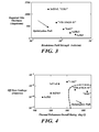
Figure 3 is a graph illustrating a relationship between breakdown field strength and film thickness of ovonic threshold switch compositions; -
Figure 4 is a graph illustrating a relationship between thermal robustness and off-state leakage currents for ovonic threshold switch compositions; -
Figure 5 is a graph illustrating a relationship between off-state leakage currents and voltage threshold bounce for ovonic threshold switch compositions; -
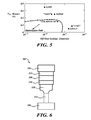
Figure 6 illustrates an enlarged cross-sectional view of a phase change memory cell according to one embodiment of the present disclosure; -
Figure 7 illustrates an enlarged cross-sectional view of an ovonic threshold switch according to another embodiment of the present disclosure; and -
Figure 8 is a block diagram of a system that includes a phase change memory having an ovonic threshold switch. - Reference throughout this specification to "one embodiment" or "an embodiment" means that a particular feature, structure, or characteristic described in connection with the embodiment is included in at least one embodiment. Thus, the appearances of the phrases "in one embodiment" or "in an embodiment" in various places throughout this specification are not necessarily all referring to the same embodiment. Furthermore, the particular features, structures, or characteristics may be combined in any suitable manner in one or more embodiments.
- In the Figures, identical reference numbers identify similar elements or acts. The size and relative positions of features in the drawings are not necessarily drawn to scale. For example, some of the various features are arbitrarily enlarged and positioned to improve drawing legibility.
- The alloy components described herein theoretically add up to an atomic percentage of 100, but the compositional ranges are determined by empirical formula.
- Referring to
Figure 1 , amemory array 100 includes a plurality ofmemory cells 102 positioned between a plurality ofbit lines 104 andword lines 106. Eachmemory cell 102 includes anovonic threshold switch 108 and amemory element 110. Both theovonic threshold switch 108 and thememory element 110 may be formed of a chalcogenide composition, an alloy of elements of group VI of the periodic table, such as Te, S, or Se. - The
memory element 110 may be a phase change material that switches from a high resistance state, generally amorphous, to a low resistance state, generally crystalline, upon the application of energy such as heat, light, voltage potential, or electrical current. The phase change material may be switched from completely amorphous to completely crystalline or between different detectable states of local order across the entire spectrum between completely amorphous and completely crystalline. - Programming the phase change material to alter its state or phase may be accomplished by applying voltage potentials across electrodes, thereby generating a voltage potential across the
ovonic threshold switch 108 and thememory element 110. When the voltage potential is greater than a threshold voltage (VTH) of theovonic threshold switch 108, an electrical current may flow through theovonic threshold switch 108 and the phase change material in thememory element 110 and may result in heating of the phase change material. This heating may alter the memory state or phase of the phase change material, thus altering the electrical characteristic of thememory element 110, e.g., the resistance. Thus, the memory material may also be referred to as a programmable resistance material. - The amorphous or semi-amorphous state may be associated with a "reset" state or a logic "0" value, while a crystalline or semi-crystalline state may be associated with a "set" state, or a logic "1" value. The resistance of memory material in the amorphous or semi-amorphous state is generally greater than the resistance of memory material in the crystalline or semi-crystalline state. It is to be appreciated that the association of reset and set with amorphous and crystalline states, respectively, is a convention and that at least an opposite convention may be adopted.
- Using an electrical current, the phase change memory material may be heated to a relatively higher temperature to amorphize memory material and "reset" memory material (e.g., program memory material to "0"). Heating the volume of memory material to a relatively lower crystallization temperature may crystallize memory material and "set" memory material (e.g., program memory material to "1 "). Various resistances of memory material may be achieved to store information by varying the amount of current flow and duration through the volume of memory material.
- The
memory elements 110 of thememory cells 102 may be connected to theword lines 106 and to thebit lines 104 through theovonic threshold switch 108. To select aparticular memory cell 102, voltage potentials may be applied across theassociated bit line 104 andword line 106. Theovonic threshold switch 108 may be used to access thememory element 110 during programming or reading operations. - In contrast to the phase change memory material in the
memory element 110, the chalcogenide material in theovonic threshold switch 108 does not change state or phase upon the application of energy. Instead, the switching material used in theovonic threshold switch 108 may be in a substantially amorphous state that may be repeatedly and reversibly switched between a higher resistance "off" state and a lower resistance "on" state. Theovonic threshold switch 108 is either on or off depending on the amount of voltage potential applied across thememory cell 102. The off state may be substantially non conductive and the on state may be substantially conductive. - The
ovonic threshold switch 108 is formed of a chalcogenide alloy that provides reproducible switching at fast switching speeds. Basic principles and operational features of ovonic threshold switches are presented, for example, inU.S. Patent Nos. 3,271,591 ;5,543,737 ;5,694,146 ; and5,757,446 ; the disclosures of which are hereby incorporated by reference, as well as in several journal articles including Ovshinsky, S.R., "Reversible Electrical Switching Phenomena in Disordered Structures," Physical Review Letters 21:1450-1453 (1969); Ovshinsky, S.R. and Fritzsche, H. , "Amorphous Semiconductors for Switching, Memory, and Imaging Applications," IEEE Transactions on Electron Devices ED-20:91-105 (1973); which are hereby incorporated by reference. Three-terminal ovonic threshold switch devices are disclosed, for example, inU.S. Patent Nos. 6,969,867 and6,967,344 ; which are hereby incorporated by reference. - The
ovonic threshold switch 108 switches between the off and the on state by applying an electrical current or voltage potential that exceeds a threshold current or threshold voltage, ITH and VTH, respectively. If a voltage potential is less than VTH of theovonic threshold switch 108, then theovonic threshold switch 108 remains in the off or highly resistive state. Little or no electrical current passes through thememory cell 102 when theovonic threshold switch 108 is in the off state. If a voltage potential greater than VTH is applied, then theovonic threshold switch 108 may switch to the on state and operate in a relatively low resistive state. In the on state, current passes through thememory cell 102 and can be used to read or program thememory element 110. -
Figure 2 illustrates an example I-V characteristic of the switching material inovonic threshold switch 108. Since the switching material of theovonic threshold switch 108 may remain in an amorphous state, the current-voltage (I-V) characteristic may remain the same throughout the operating life of theovonic threshold switch 108. - When the voltage across the
ovonic threshold switch 108 is less than the threshold voltage, VTH, theovonic threshold switch 108 is in a substantially nonconductive state, i.e., anoff state curve 112. If a voltage potential greater than VTH or a current greater than ITH is applied, then theovonic threshold switch 108 turns on, i.e., an onstate curve 114. If the voltage potential across theovonic threshold switch 108 is greater than VTH, then the voltage potential across theovonic threshold switch 108 may drop or snapback to a holding voltage potential, VH. - As current passing through the
ovonic threshold switch 108 increases, the voltage potential across theovonic threshold switch 108 may remain close to VH, see the onstate curve 114. Theovonic threshold switch 108 may remain in the on state until the current decreases to below a holding current IH. Once the current falls below IH, theovonic threshold switch 108 may turn off and return to the highly resistive state. In order to switch theovonic threshold switch 108 back to the on state, a voltage greater than or equal to the threshold voltage must be applied across theovonic threshold switch 108. - In the
off state 112, the current across theovonic threshold switch 108 increases only a small amount as the voltage potential is increased. When the voltage potential exceeds the VTH the switching material instantaneously switches from the off state to the on state, which is illustrated by the dashed line. Upon switching, the voltage through theovonic threshold switch 108 decreases significantly to the holding voltage, VH. At this point wherein voltage across theovonic threshold switch 108 is at or near the holding voltage VH, the current becomes more sensitive to changes in the voltage. Therefore, the curve of the onstate 114 has a steeper slope than theoff state curve 112. - The present disclosure is directed to an ovonic threshold switch film composition that can sustain high field strength and provide low off state leakage with stable threshold voltages, VTH. The
ovonic threshold switch 108 is a chalcogenide alloy that includes tellurium, sulfur, arsenic, germanium, and selenium, which will be referred to as TSLAGS. The TSLAGSovonic threshold switch 108 composition also includes silicon and may be formed with or without nitrogen. - The TSLAGS composition for the
ovonic threshold switch 108 may be formed by combining several alloys together. For example, the TSLAGS composition may be started by first forming a number of binary alloys. More specifically, an alloy of arsenic and sulfur can be prepared that has proportions ranging from 30% to 45% and from 55% to 70%, respectively. In addition, another alloy may be formed that includes arsenic and selenium having proportions ranging from 30% to 45% and from 55% to 70%, respectively. An additional alloy may be formed that includes arsenic and tellurium combined having proportions ranging from 30% to 45% and from 55% to 70%, respectively. In one embodiment, these binary chalcogenide alloys of arsenic/sulfur, arsenic/selenium, and arsenic/tellurium are As2S3, As2Se3, and As2Te3, respectively. - After forming the binary alloys of arsenic/sulfur, arsenic/selenium, and arsenic/tellurium, a quaternary alloy comprising arsenic, sulfur, selenium, and tellurium may be formed. For example, the binary alloys of arsenic/sulfur, arsenic/selenium, and arsenic/tellurium can be combined to form a single alloy of As, Se, S, Te, in which the element-pair sulfur/selenium have proportions ranging from 20% to 80% and from 20% to 80%, respectively. In addition, the element-pair of sulfur/tellurium have proportions ranging from 10% to 50%, and from 50% to 90%, respectively, and the element-pair of selenium/tellurium have proportions ranging from 10% to 50% and from 50% to 90%, respectively.
- Therefore, quaternary alloys of arsenic/sulfur/selenium/tellurium may also be formed according to the previously described proportions. More particularly, sulfur, selenium, and tellurium are interchangeable so that the proportions of these three elements to each other may be varied with in the parameters discussed above with respect to tertiary combinations with the binary alloys arsenic/sulfur, arsenic/selenium, and arsenic/tellurium. The elements sulfur, selenium, and tellurium may be used interchangeably in the percentages described above since these elements form similar crystalline structures and arrange in the same lattice positions.
- In order to improve thermal robustness of these tertiary and quaternary alloys, germanium may be added in the range of 10% to 40% and silicon may be added in the range of 5% to 18%. Germanium and silicon may be incorporated in various ways, such as composite-target incorporation, cosputtering, and metal organic chemical vapor deposition (MOCVD). The incorporation of silicon provides compatibility with high-temperature integrated circuit back-end fabrication processing.
- Additionally, the incorporation of nitrogen, N2, into the
ovonic threshold switch 108 alloy composition improves the alloy's leakage characteristics, the stability of the alloy's threshold voltage, the alloy's thermal robustness, and the alloy's cycle life. Nitrogen may be added to the TSLAGS ovonic threshold switch alloys above in the range of 0% to 10% to enhance theovonic threshold switch 108 characteristics. Nitrogen may be incorporated through reactive sputtering, composite-target incorporation, or other suitable processes. - This TSLAGS ovonic threshold switch composition having silicon with or without the inclusion of nitrogen balances the key functional requirements and minimizes off-state leakage and sub-threshold I-V swing, variation of the threshold voltage over many cycles, drift of the threshold voltage with delay time between pulses, and optimizes cycle life and operating current densities. In addition, the TSLAGS composition provides high thermal robustness needed for integration into back-end fab-processing.
- Breakdown field strengths are the major intrinsic property that relates to the threshold voltage needed for switching of ovonic threshold switches. As illustrated in
Figure 3 , different ovonic threshold switch compositions have different breakdown field strengths. Traditional binary chalcogenide alloys, such as As2S3 and As2Se3 have relatively high field strengths, between 1x10⁶ and 1x10⁷ volts/centimeter. Strong field strength alloys, such as As2S3 and As2Se3, require less film thickness to be deposited than weak field strength alloys, in order to achieve a given threshold voltage target. Other binary chalcogenide alloys, such as As2Te3 have relatively low field strengths, between 1x10⁵ and 1x10⁶ volts/centimeter. Therefore As2Te3 alloys require thicker films to achieve desired threshold voltages. - In one embodiment, the TSLAGS ovonic threshold switch composition with nitrogen and silicon can achieve a threshold voltage, VTH, of 4.5V at a film thickness of 600 Angstroms. The breakdown field strength of this TSLAGS composition is not as high as the As2S3 and As2Se3 alloys and not as low as the As2Te3 alloys. Therefore, the TSLAGS composition does not require a film thickness as large as the alloy, As2Te3.
- Other critical performance parameters for ovonic threshold switch applications include thermal robustness and off-state leakage. Chalcogenide alloys must be thermally robust in order to be feasibly integrated into a semiconductor process sequence, due to high-temperature steps that occur during back-end steps of device fabrication. It is advantageous to maximize the temperature an alloy can withstand before sublimating into the surrounding space, delaminating from adjacent film layers, or otherwise forfeiting its desired electrical properties. An alloy should be able to withstand temperatures of at least 300-350 degrees Celsius for integration into most existing process technologies.
- As illustrated in
Figure 4 , the alloy, As2S3, has the lowest thermal robustness at around 150 degrees Celsius. In addition, the alloys As2Te3 and As2Se3 yield a thermal robustness rating less than 300 degrees Celsius. Adding germanium to As2Te3 and As2Se3, "TAG" and "SAG", respectively, increases the robustness ratings to at or above 300 degrees Celsius. A higher proportion of germanium in the whole chalcogenide alloy results in improved thermal robustness. For example, incorporating 40% germanium results in significantly less delamination after an anneal at 350 degrees Celsius than 10% germanium. - Advantageously, the TSLAGS composition with nitrogen and silicon also achieves a desirable thermal robustness of approximately 350 degrees Celsius. A higher proportion of silicon also improves the thermal robustness of the chalcogenide alloy. For example, incorporating 10% silicon into the whole alloy reduces occurrence of delaminations during an anneal at 350 degrees Celsius, as compared to only 5% silicon.
- Another parameter that is optimized by the TSLAGS ovonic threshold switch material having silicon and formed with or without nitrogen is the off-state leakage current. By minimizing the off-state leakage current, the power consumption of
unselected memory elements 102 is minimized. The off-state leakage current is strongly related to the alloy's field strength, i.e., the higher the field strength the lower the off-state leakage current. Incorporation of nitrogen, in particular, reduces the off-state leakage current of the alloy. For example, an inclusion of 2% nitrogen can decrease the off-state leakage current. - Advantageously, introduction of nitrogen also improves the thermal robustness of the ovonic threshold switch. A higher proportion of nitrogen, such as 4%, reduces the occurrence of delamination at an anneal of 350 degrees Celsius, as compared to 2% nitrogen.
- In addition to the improved thermal robustness, the TSLAGS composition optimizes ovonic threshold switch performance by having a desirable field strength and therefore a lower off-state leakage current. As an example, an application involving a large memory arrays may require an ovonic threshold switch to have a diameter of 150nm (Area = 1.8*10-10 cm2) and a maximum off-state leakage of about 5x10⁻⁹ Amperes. The TSLAGS composition with nitrogen and silicon satisfies the leakage requirements for this application and achieves the desired thermal robustness specifications.
- Another parameter that should be minimized in order to optimize performance of the
ovonic threshold switch 108 is the bounce of the threshold voltage, VTH, i.e., the variation or range between switching cycles. A VTH-bounce of 0.3 Volts is considered the highest-acceptable amount of variation. As illustrated inFigure 5 , high field strength alloys, such as As2S3 have a high VTH- bounce, while lower field strength alloys, such as As2Te3 tend to have less VTH-bounce. The TSLAGS composition with nitrogen and silicon achieve the desired off-state leakage current while having an acceptable VTH-bounce of approximately 0.3 Volts. In one embodiment, the measurement for VTH-bounce was performed by applying 30 consecutive square pluses of 500ns width and capturing the VTH-bounce with an oscilloscope. - Referring to
Figure 6 , a phasechange memory cell 302 includes aphase change layer 310 and a TSLAGSovonic threshold switch 308 having silicon formed with or without nitrogen. Theovonic threshold switch 308 is positioned between a top and a bottom electrode, 312 and 314, respectively. Amiddle electrode 316 is located between thephase change layer 310 and theovonic threshold switch 308. Thetop electrode 312 is aligned with abitline 304 and separates thebitline 304 from theovonic threshold switch 308. Thephase change layer 310 is in direct contact with thebottom electrode 314, which is in direct contact with awordline 306. - The
phase change layer 310 is typically formed with one or more chalcogenide elements (i.e., Group VI elements from the periodic table), as described above. One common chalcogenide combination is GST (germanium - Antimony- tellurium). However, any known suitable phase change material may be used. - The bitline and wordline
layers layers threshold switch layer 308. Some examples of copper barrier materials that can be employed include cobalt, ruthenium, tantalum, tantalum nitride, indium oxide, tungsten nitride, titanium, titanium tungsten, titanium nitride, silicon carbide, polycrystalline silicon, or other suitable conductors or resistive conductors compatible withovonic threshold switch 308. - Programming of the phase
change memory cell 302 occurs by pulses of current applied between thebitline 304 and thewordline 306. In one embodiment, the programming current rises from zero to the "reset" current value and holds the "reset" current value for up to 100ns to melt thephase change layer 310. In some embodiments, in order to obtain effective cooling of the moltenphase change layer 310, the current pulse decreases to 50%-80% of the "reset" current value for 10-100 ns before returning to zero. The reduction in the programming current to 50-80% of the reset current value ensures that the ovonic threshold switch layers 308 remains in the on state, i.e. conductive while thephase change layer 310 begins cooling. The step down in programming current more effectively quenches thephase change layer 310 to a vitreous (amorphous) state by removing the heat in thephase change layer 310 through the highly conductiveovonic threshold switch 308 to the thermal sinks of thebitline 304 andwordline 306. - The cooling stage determines if the
phase change layer 310 solidifies in a high or low resistive state. A faster cooling process arranges thephase change layer 310 in the high resistance state, the "reset" state. A slower cooling process arranges thephase change layer 310 in the low resistance state, the "set" state. - In one embodiment, an
ovonic threshold switch 400 may be formed as illustrated inFigure 7 . Afirst oxide layer 420 may be deposited or grown on asubstrate 418, which may be a silicon wafer. Thefirst oxide layer 420 may be silicon dioxide or any other suitable insulating material. In one embodiment, thefirst oxide layer 420 is 4000 Angstroms thick (400 nanometers). Subsequently, abottom electrode layer 414 is deposited over thefirst oxide layer 420 and may have a thickness of 500 Angstroms (50 nanometers). In one embodiment, thebottom electrode layer 414 is 397 Angstroms (39.7 nanometers) in thickness. Thebottom electrode 414 may be formed of any suitable conductive material as described above. - Subsequently, a
second oxide layer 422 may be deposited over thebottom electrode layer 414. Thesecond oxide layer 422 may also be a silicon dioxide or other suitable insulating layer. - The layers on the
substrate 418 may then be subjected to a densification process at 525 degrees Celsius for one minute. After the densification process is complete, a photoresist layer (not shown) may be deposited over thebottom electrode layer 414 to define a pore or viaregion 424. After a pattern and etch step to remove portions of thesecond oxide layer 422, a top surface 415 of thebottom electrode 414 is exposed by the viaregion 424. The viaregion 424 is defined by sidewalls 417. The photoresist layer may be removed after the viaregion 424 is formed. - In one embodiment, a dilute hydrogen fluoride pore clean may be used to prepare the
second oxide layer 422 for deposition of an ovonicthreshold switch layer 408. The ovonicthreshold switch layer 408 is a deposition of a TSLAGS composition having silicon with or without nitrogen according to an embodiment the present disclosure. The ovonicthreshold switch layer 408 may be formed by sputter deposition with reactive nitrogen to a thickness of 675 Angstroms (67.5 nanometers). The TSLAGS ovonic threshold switch film may be formed using other thin film deposition techniques such as, chemical vapor deposition or physical vapor deposition. In one embodiment the ovonicthreshold switch layer 408 includes 8% silicon and has a thickness of 679 Angstroms. Preferably, the ovonicthreshold switch layer 408 conforms to the sidewalls 417 of the via 424 and the top surface 415 of thebottom electrode 414. The ovonicthreshold switch layer 408 may directly contact thebottom electrode 414 on the top surface 415. - Subsequently, a
top electrode 412 is deposited over the ovonicthreshold switch layer 408 and may be 406 Angstroms in thickness. In addition, a probe pad metal layer 426 may be deposited over thetop electrode 412 and in thevia 424. Photoresist layers and etch steps may be used to define active areas and to define contact pads. - The
ovonic threshold switch 400 may then be heated in a convection oven anneal process at 350°C for thirty minutes. It should be noted that this is an exemplary embodiment and other suitable methods may be used to form theovonic threshold switch 400. - Turning to
Figure 8 , a portion of asystem 500 in accordance with an embodiment of the present disclosure is described.System 500 may be used in wireless devices such as a personal digital assistant, a laptop or portable computer with wireless capability, a web tablet, a wireless telephone, a pager, an instant messaging device, a digital music player, a digital camera, or other devices that may be adapted to transmit and/or receive information wirelessly. Thesystem 500 may be used in any of the following systems: a wireless local area network (WLAN) system, a wireless personal area network (WPAN) system, or a cellular network, although the scope of the present invention is not limited in this respect. - The
system 500 may include acontroller 510, an input/output (I/O) device 520 (e.g., a keypad, display), static random access memory (SRAM) 460, amemory 530, and awireless interface 540 coupled to each other via abus 550. A battery 480 may be used in some embodiments. It should be noted that the scope of the present invention is not limited to embodiments having any or all of these components. - The
controller 510 may comprise, for example, one or more microprocessors, digital signal processors, microcontrollers, or the like. Thememory 530 may be used to store messages transmitted to or bysystem 500. Thememory 530 may also optionally be used to store instructions that are executed bycontroller 510 during the operation ofsystem 500, and may be used to store user data. Thememory 530 may be provided by one or more different types of memory. For example,memory 530 may comprise any type of random access memory, a volatile memory, a non-volatile memory such as a flash memory and/or a memory discussed herein. - I/
O device 520 may be used by a user to generate a message. Thesystem 500 may usewireless interface 540 to transmit and receive messages to and from a wireless communication network with a radio frequency (RF) signal. Examples ofwireless interface 540 may include an antenna or a wireless transceiver, although the scope of the present invention is not limited in this respect. - One example of the TSLAGS material having nitrogen and 8% silicon formed as a 500 Angstrom thick film with a 150nm diameter achieved an average threshold voltage of 3.29 Volts, an average holding voltage of 1.02 Volts, an average voltage snapback of 1.90, and a current snapback of 0.39 milliamperes.
- In one embodiment, the TSLAGS composition with silicon and nitrogen may comprise an arsenic concentration in the range of 9-39%, a germanium concentration in the range of 10-40%, a silicon concentration in the range of 5-18%, a nitrogen concentration in the range of 0-10%, and a combination of selenium, sulfur, and tellurium in a concentration in the range of 17-60%. The ratio of sulfur to selenium is in the range of 0.25 and 4 and the ratio of sulfur to tellurium is in the range of 0.11 and 1. In these examples, the percentages are atomic percentages which total 100% of the atoms of the constituent elements.
- In one embodiment, the
ovonic threshold switch 108 is a chalcogenide composition of AS25-27S5-6Se12-13 Te28-30Ge17-19Si7-10N0-5. In alternative embodiments, theovonic threshold switch 108 may be As25S5.5Se12.2Te28.1 Ge17.8Si7.1N4.1, As26.17S5.78Se12.75Te29.38Ge18.56Si7.37, As25.4S5.6Se12.3Te28.6Ge18.1Si9.6, and As25.53S5.6Se12.37Te28.69Ge18.18Si9.64. It should be noted that impurities may be incorporated into any of the alloys during formation. For example, in the alloy composition As25S5.5Se12.2Te28.1Ge17.8Si7.1N4.1, 0.4% of the total composition is an impurity. - The various embodiments described above can be combined to provide further embodiments. All of the U.S. patents, U.S. patent application publications, U.S. patent application, foreign patents, foreign patent application and non-patent publications referred to in this specification and/or listed in the Application Data Sheet are incorporated herein by reference, in their entirety. Aspects of the embodiments can be modified, if necessary to employ concepts of the various patents, application and publications to provide yet further embodiments.
- These and other changes can be made to the embodiments in light of the above-detailed description. In general, in the following claims, the terms used should not be construed to limit the claims to the specific embodiments disclosed in the specification and the claims, but should be construed to include all possible embodiments along with the full scope of equivalents to which such claims are entitled. Accordingly, the claims are not limited by the disclosure.
- The various embodiments described above can be combined to provide further embodiments. These and other changes can be made to the embodiments in light of the above-detailed description. In general, in the following claims, the terms used should not be construed to limit the claims to the specific embodiments disclosed in the specification and the claims, but should be construed to include all possible embodiments along with the full scope of equivalents to which such claims are entitled. Accordingly, the claims are not limited by the disclosure.
Claims (14)
- A chalcogenide alloy, comprising:AsmXqGerSitNz
wherein:m is an atomic percentage of the alloy in the range of 9 to 39;q is an atomic percentage of the alloy in the range of 17 and 60;r is an atomic percentage of the alloy in the range of 10 and 40;t is an atomic percentage of the alloy in the range of 5 and 18;z is an atomic percentage of the alloy in the range of 0 and 10;X is SaSedTeg wherein,
a/d is in the range of 0.25 and 4; and
a/g is in the range of 0.11 and 1. - The chalcogenide alloy of claim 1, comprising:AS25-27S5-6Se12-13Te28-30Ge17-19Si7-10N0-5.
- The chalcogenide alloy of claim 1, comprising:As25S5.5Se12.2Te28.1Ge17.8Si7.1N4.1.
- The chalcogenide alloy of claim 1, comprising:AS26.17S5.78Se12.75Te29.38Ge18.56Si7.37.
- The chalcogenide alloy of claim 1, comprising:AS25.53S5.6Se12.37Te28.69Ge18.18Si9.64.
- The chalcogenide alloy of claim 1, comprising:AS25.4S5.6Se12.3Te28.6Ge18.1S19.6.
- An ovonic threshold switch, comprising:
a chalcogenide alloy having the following formula:AsmXqGerSitNz
wherein:m is an atomic percentage of the alloy in the range of 9 to 39;q is an atomic percentage of the alloy in the range of 17 and 60;r is an atomic percentage of the alloy in the range of 10 and 40;t is an atomic percentage of the alloy in the range of 5 and 18;z is an atomic percentage of the alloy in the range of 0 and 10;X is SaSedTeg wherein,
a/d is in the range of 0.25 and 4; and
a/g is in the range of 0.11 and 1. - The ovonic threshold switch of claim 7, comprising:AS25-27S5-6Se12-13Te28-30Ge17-19Si7-10N0-5.
- The ovonic threshold switch of claim 7, comprising:AS25S5.5Se12.2Te28.1Ge17.8Si7.1N4.1.
- The ovonic threshold switch of claim 7, comprising:AS26.17S5.78Sei2.75Te29.38Gei8.56Si7.37.
- The ovonic threshold switch of claim 7, comprising:AS25.53S5.6Se12.37Te28.69Ge18.18Si9.64.
- The ovonic threshold switch of claim 7, comprising:AS25.4S5.6Se12.3Te28.6Ge18.1Si9.6.
- A phase change memory cell, comprising:a phase change memory layer; andan ovonic threshold switch layer formed of a chalcogenide alloy according to any of claims 1 to 6
- A memory, comprising:a wordline;a bitline;a phase change memory layer;a first electrode that separates the phase change memory layer from the wordline;an ovonic threshold switch layer formed of a chalcogenide alloy according to any of claims 1 to 6,a second electrode that separates the ovonic threshold switch from the phase change memory layer; anda third electrode that separates the ovonic threshold switch from the bitline.
Applications Claiming Priority (2)
| Application Number | Priority Date | Filing Date | Title |
|---|---|---|---|
| US14159608P | 2008-12-30 | 2008-12-30 | |
| US12/637,644 US8148707B2 (en) | 2008-12-30 | 2009-12-14 | Ovonic threshold switch film composition for TSLAGS material |
Publications (3)
| Publication Number | Publication Date |
|---|---|
| EP2204851A2 true EP2204851A2 (en) | 2010-07-07 |
| EP2204851A3 EP2204851A3 (en) | 2013-01-09 |
| EP2204851B1 EP2204851B1 (en) | 2014-06-25 |
Family
ID=42084542
Family Applications (1)
| Application Number | Title | Priority Date | Filing Date |
|---|---|---|---|
| EP09180927.7A Active EP2204851B1 (en) | 2008-12-30 | 2009-12-30 | Ovonic threshold switch film composition for TSLAGS material |
Country Status (2)
| Country | Link |
|---|---|
| US (1) | US8148707B2 (en) |
| EP (1) | EP2204851B1 (en) |
Cited By (2)
| Publication number | Priority date | Publication date | Assignee | Title |
|---|---|---|---|---|
| CN107068858A (en) * | 2017-01-25 | 2017-08-18 | 中国科学院上海微系统与信息技术研究所 | Phase-change material, gate driver part for gate driver part and preparation method thereof |
| FR3119270A1 (en) | 2021-01-27 | 2022-07-29 | Stmicroelectronics S.R.L. | switching cell |
Families Citing this family (28)
| Publication number | Priority date | Publication date | Assignee | Title |
|---|---|---|---|---|
| US8030734B2 (en) * | 2008-12-30 | 2011-10-04 | Stmicroelectronics S.R.L. | Forming phase change memories with a breakdown layer sandwiched by phase change memory material |
| US8728940B2 (en) | 2012-01-26 | 2014-05-20 | Micron Technology, Inc. | Memory arrays and methods of forming same |
| US9136307B2 (en) | 2012-02-09 | 2015-09-15 | Micron Technology, Inc. | Memory cells and memory cell formation methods using sealing material |
| CN103489478B (en) * | 2012-06-12 | 2018-09-25 | 中国科学院上海微系统与信息技术研究所 | A kind of phase transition storage |
| US8885382B2 (en) | 2012-06-29 | 2014-11-11 | Intel Corporation | Compact socket connection to cross-point array |
| US8841649B2 (en) * | 2012-08-31 | 2014-09-23 | Micron Technology, Inc. | Three dimensional memory array architecture |
| US8729523B2 (en) | 2012-08-31 | 2014-05-20 | Micron Technology, Inc. | Three dimensional memory array architecture |
| CN102832338B (en) * | 2012-09-06 | 2015-10-07 | 中国科学院上海微系统与信息技术研究所 | A kind of limiting structure phase transition storage and preparation method thereof |
| US20140262028A1 (en) | 2013-03-13 | 2014-09-18 | Intermolecular, Inc. | Non-Contact Wet-Process Cell Confining Liquid to a Region of a Solid Surface by Differential Pressure |
| KR101431656B1 (en) | 2013-04-05 | 2014-08-21 | 한국과학기술연구원 | Chacogenide switching device using germanium and selenium and manufacture method thereof |
| US20150028280A1 (en) * | 2013-07-26 | 2015-01-29 | Micron Technology, Inc. | Memory cell with independently-sized elements |
| US9443763B2 (en) | 2013-09-12 | 2016-09-13 | Micron Technology, Inc. | Methods for forming interconnections between top electrodes in memory cells by a two-step chemical-mechanical polishing (CMP) process |
| KR102532201B1 (en) | 2016-07-22 | 2023-05-12 | 삼성전자 주식회사 | Memory device |
| US10889887B2 (en) | 2016-08-22 | 2021-01-12 | Honeywell International Inc. | Chalcogenide sputtering target and method of making the same |
| JP7079201B2 (en) * | 2016-10-04 | 2022-06-01 | ソニーセミコンダクタソリューションズ株式会社 | Switch elements and storage devices and memory systems |
| US10892413B2 (en) * | 2017-01-17 | 2021-01-12 | International Business Machines Corporation | Integration of confined phase change memory with threshold switching material |
| US10461125B2 (en) | 2017-08-29 | 2019-10-29 | Micron Technology, Inc. | Three dimensional memory arrays |
| US10374009B1 (en) * | 2018-07-17 | 2019-08-06 | Macronix International Co., Ltd. | Te-free AsSeGe chalcogenides for selector devices and memory devices using same |
| US10978639B2 (en) * | 2018-08-14 | 2021-04-13 | Newport Fab, Llc | Circuits for reducing RF signal interference and for reducing DC power loss in phase-change material (PCM) RF switches |
| KR102636534B1 (en) | 2018-08-20 | 2024-02-15 | 에스케이하이닉스 주식회사 | Chalcogenide material and electronic device including the same |
| KR102635268B1 (en) * | 2018-08-20 | 2024-02-13 | 에스케이하이닉스 주식회사 | Chacogenide material and electronic device including the same |
| CN109473411B (en) * | 2018-09-17 | 2021-08-20 | 上海音特电子有限公司 | Thin film material for integrated circuit input/output pin overvoltage protection and use method |
| CN111326651A (en) * | 2018-12-17 | 2020-06-23 | 中国科学院上海微系统与信息技术研究所 | OTS material, gating unit and preparation method thereof |
| US11289540B2 (en) | 2019-10-15 | 2022-03-29 | Macronix International Co., Ltd. | Semiconductor device and memory cell |
| US11158787B2 (en) | 2019-12-17 | 2021-10-26 | Macronix International Co., Ltd. | C—As—Se—Ge ovonic materials for selector devices and memory devices using same |
| US20210249600A1 (en) * | 2020-02-11 | 2021-08-12 | Macronix International Co., Ltd. | Phase change memory with a carbon buffer layer |
| US11362276B2 (en) | 2020-03-27 | 2022-06-14 | Macronix International Co., Ltd. | High thermal stability SiOx doped GeSbTe materials suitable for embedded PCM application |
| US11271036B2 (en) | 2020-06-24 | 2022-03-08 | Sandisk Technologies Llc | Memory device containing dual etch stop layers for selector elements and method of making the same |
Citations (20)
| Publication number | Priority date | Publication date | Assignee | Title |
|---|---|---|---|---|
| US3271591A (en) | 1963-09-20 | 1966-09-06 | Energy Conversion Devices Inc | Symmetrical current controlling device |
| US3530441A (en) | 1969-01-15 | 1970-09-22 | Energy Conversion Devices Inc | Method and apparatus for storing and retrieving information |
| US5166758A (en) | 1991-01-18 | 1992-11-24 | Energy Conversion Devices, Inc. | Electrically erasable phase change memory |
| US5296716A (en) | 1991-01-18 | 1994-03-22 | Energy Conversion Devices, Inc. | Electrically erasable, directly overwritable, multibit single cell memory elements and arrays fabricated therefrom |
| US5341328A (en) | 1991-01-18 | 1994-08-23 | Energy Conversion Devices, Inc. | Electrically erasable memory elements having reduced switching current requirements and increased write/erase cycle life |
| US5359205A (en) | 1991-11-07 | 1994-10-25 | Energy Conversion Devices, Inc. | Electrically erasable memory elements characterized by reduced current and improved thermal stability |
| US5414271A (en) | 1991-01-18 | 1995-05-09 | Energy Conversion Devices, Inc. | Electrically erasable memory elements having improved set resistance stability |
| US5534712A (en) | 1991-01-18 | 1996-07-09 | Energy Conversion Devices, Inc. | Electrically erasable memory elements characterized by reduced current and improved thermal stability |
| US5536947A (en) | 1991-01-18 | 1996-07-16 | Energy Conversion Devices, Inc. | Electrically erasable, directly overwritable, multibit single cell memory element and arrays fabricated therefrom |
| US5543737A (en) | 1995-02-10 | 1996-08-06 | Energy Conversion Devices, Inc. | Logical operation circuit employing two-terminal chalcogenide switches |
| US5596522A (en) | 1991-01-18 | 1997-01-21 | Energy Conversion Devices, Inc. | Homogeneous compositions of microcrystalline semiconductor material, semiconductor devices and directly overwritable memory elements fabricated therefrom, and arrays fabricated from the memory elements |
| US5687112A (en) | 1996-04-19 | 1997-11-11 | Energy Conversion Devices, Inc. | Multibit single cell memory element having tapered contact |
| US5694146A (en) | 1994-10-14 | 1997-12-02 | Energy Conversion Devices, Inc. | Active matrix LCD array employing thin film chalcogenide threshold switches to isolate individual pixels |
| US5757446A (en) | 1994-10-14 | 1998-05-26 | Energy Conversion Devices, Inc. | Liquid crystal display matrix array employing ovonic threshold switching devices to isolate individual pixels |
| US5825046A (en) | 1996-10-28 | 1998-10-20 | Energy Conversion Devices, Inc. | Composite memory material comprising a mixture of phase-change memory material and dielectric material |
| US5912839A (en) | 1998-06-23 | 1999-06-15 | Energy Conversion Devices, Inc. | Universal memory element and method of programming same |
| US6087674A (en) | 1996-10-28 | 2000-07-11 | Energy Conversion Devices, Inc. | Memory element with memory material comprising phase-change material and dielectric material |
| US6671710B2 (en) | 2002-05-10 | 2003-12-30 | Energy Conversion Devices, Inc. | Methods of computing with digital multistate phase change materials |
| US6967344B2 (en) | 2003-03-10 | 2005-11-22 | Energy Conversion Devices, Inc. | Multi-terminal chalcogenide switching devices |
| US6969867B2 (en) | 2003-03-10 | 2005-11-29 | Energy Conversion Devices, Inc. | Field effect chalcogenide devices |
Family Cites Families (14)
| Publication number | Priority date | Publication date | Assignee | Title |
|---|---|---|---|---|
| US3748501A (en) | 1971-04-30 | 1973-07-24 | Energy Conversion Devices Inc | Multi-terminal amorphous electronic control device |
| GB1490986A (en) * | 1975-02-28 | 1977-11-09 | Gen Electric Co Ltd | Electric current controlling devices |
| US4845533A (en) | 1986-08-22 | 1989-07-04 | Energy Conversion Devices, Inc. | Thin film electrical devices with amorphous carbon electrodes and method of making same |
| US5177567A (en) * | 1991-07-19 | 1993-01-05 | Energy Conversion Devices, Inc. | Thin-film structure for chalcogenide electrical switching devices and process therefor |
| US6709958B2 (en) * | 2001-08-30 | 2004-03-23 | Micron Technology, Inc. | Integrated circuit device and fabrication using metal-doped chalcogenide materials |
| US6795338B2 (en) | 2002-12-13 | 2004-09-21 | Intel Corporation | Memory having access devices using phase change material such as chalcogenide |
| US7426135B2 (en) | 2005-06-22 | 2008-09-16 | Ovonyx, Inc. | Static random access memory cell using chalcogenide |
| US7499315B2 (en) | 2003-06-11 | 2009-03-03 | Ovonyx, Inc. | Programmable matrix array with chalcogenide material |
| US6992369B2 (en) | 2003-10-08 | 2006-01-31 | Ovonyx, Inc. | Programmable resistance memory element with threshold switching material |
| US7495944B2 (en) | 2005-03-30 | 2009-02-24 | Ovonyx, Inc. | Reading phase change memories |
| US8188454B2 (en) | 2005-10-28 | 2012-05-29 | Ovonyx, Inc. | Forming a phase change memory with an ovonic threshold switch |
| US7973384B2 (en) * | 2005-11-02 | 2011-07-05 | Qimonda Ag | Phase change memory cell including multiple phase change material portions |
| US8637342B2 (en) | 2005-11-10 | 2014-01-28 | Ovonyx, Inc. | Phase change memory with threshold switch select device |
| US7414883B2 (en) * | 2006-04-20 | 2008-08-19 | Intel Corporation | Programming a normally single phase chalcogenide material for use as a memory or FPLA |
-
2009
- 2009-12-14 US US12/637,644 patent/US8148707B2/en active Active
- 2009-12-30 EP EP09180927.7A patent/EP2204851B1/en active Active
Patent Citations (21)
| Publication number | Priority date | Publication date | Assignee | Title |
|---|---|---|---|---|
| US3271591A (en) | 1963-09-20 | 1966-09-06 | Energy Conversion Devices Inc | Symmetrical current controlling device |
| US3530441A (en) | 1969-01-15 | 1970-09-22 | Energy Conversion Devices Inc | Method and apparatus for storing and retrieving information |
| US5596522A (en) | 1991-01-18 | 1997-01-21 | Energy Conversion Devices, Inc. | Homogeneous compositions of microcrystalline semiconductor material, semiconductor devices and directly overwritable memory elements fabricated therefrom, and arrays fabricated from the memory elements |
| US5166758A (en) | 1991-01-18 | 1992-11-24 | Energy Conversion Devices, Inc. | Electrically erasable phase change memory |
| US5296716A (en) | 1991-01-18 | 1994-03-22 | Energy Conversion Devices, Inc. | Electrically erasable, directly overwritable, multibit single cell memory elements and arrays fabricated therefrom |
| US5341328A (en) | 1991-01-18 | 1994-08-23 | Energy Conversion Devices, Inc. | Electrically erasable memory elements having reduced switching current requirements and increased write/erase cycle life |
| US5414271A (en) | 1991-01-18 | 1995-05-09 | Energy Conversion Devices, Inc. | Electrically erasable memory elements having improved set resistance stability |
| US5534712A (en) | 1991-01-18 | 1996-07-09 | Energy Conversion Devices, Inc. | Electrically erasable memory elements characterized by reduced current and improved thermal stability |
| US5536947A (en) | 1991-01-18 | 1996-07-16 | Energy Conversion Devices, Inc. | Electrically erasable, directly overwritable, multibit single cell memory element and arrays fabricated therefrom |
| US5359205A (en) | 1991-11-07 | 1994-10-25 | Energy Conversion Devices, Inc. | Electrically erasable memory elements characterized by reduced current and improved thermal stability |
| US5694146A (en) | 1994-10-14 | 1997-12-02 | Energy Conversion Devices, Inc. | Active matrix LCD array employing thin film chalcogenide threshold switches to isolate individual pixels |
| US5757446A (en) | 1994-10-14 | 1998-05-26 | Energy Conversion Devices, Inc. | Liquid crystal display matrix array employing ovonic threshold switching devices to isolate individual pixels |
| US5543737A (en) | 1995-02-10 | 1996-08-06 | Energy Conversion Devices, Inc. | Logical operation circuit employing two-terminal chalcogenide switches |
| US5687112A (en) | 1996-04-19 | 1997-11-11 | Energy Conversion Devices, Inc. | Multibit single cell memory element having tapered contact |
| US5825046A (en) | 1996-10-28 | 1998-10-20 | Energy Conversion Devices, Inc. | Composite memory material comprising a mixture of phase-change memory material and dielectric material |
| US6087674A (en) | 1996-10-28 | 2000-07-11 | Energy Conversion Devices, Inc. | Memory element with memory material comprising phase-change material and dielectric material |
| US5912839A (en) | 1998-06-23 | 1999-06-15 | Energy Conversion Devices, Inc. | Universal memory element and method of programming same |
| US6671710B2 (en) | 2002-05-10 | 2003-12-30 | Energy Conversion Devices, Inc. | Methods of computing with digital multistate phase change materials |
| US6714954B2 (en) | 2002-05-10 | 2004-03-30 | Energy Conversion Devices, Inc. | Methods of factoring and modular arithmetic |
| US6967344B2 (en) | 2003-03-10 | 2005-11-22 | Energy Conversion Devices, Inc. | Multi-terminal chalcogenide switching devices |
| US6969867B2 (en) | 2003-03-10 | 2005-11-29 | Energy Conversion Devices, Inc. | Field effect chalcogenide devices |
Non-Patent Citations (2)
| Title |
|---|
| OVSHINSKY, S.R.: "Reversible Electrical Switching Phenomena in Disordered Structures", PHYSICAL REVIEW LETTERS, vol. 21, 1969, pages 1450 - 1453 |
| OVSHINSKY, S.R.; FRITZSCHE, H.: "Amorphous Semiconductors for Switching, Memory, and Imaging Applications", IEEE TRANSACTIONS ON ELECTRON DEVICES ED, vol. 20, 1973, pages 91 - 105 |
Cited By (3)
| Publication number | Priority date | Publication date | Assignee | Title |
|---|---|---|---|---|
| CN107068858A (en) * | 2017-01-25 | 2017-08-18 | 中国科学院上海微系统与信息技术研究所 | Phase-change material, gate driver part for gate driver part and preparation method thereof |
| FR3119270A1 (en) | 2021-01-27 | 2022-07-29 | Stmicroelectronics S.R.L. | switching cell |
| EP4036997A1 (en) | 2021-01-27 | 2022-08-03 | STMicroelectronics S.r.l. | Switching cell |
Also Published As
| Publication number | Publication date |
|---|---|
| US8148707B2 (en) | 2012-04-03 |
| US20100163822A1 (en) | 2010-07-01 |
| EP2204851A3 (en) | 2013-01-09 |
| EP2204851B1 (en) | 2014-06-25 |
Similar Documents
| Publication | Publication Date | Title |
|---|---|---|
| EP2204851B1 (en) | Ovonic threshold switch film composition for TSLAGS material | |
| US7282730B2 (en) | Forming a carbon layer between phase change layers of a phase change memory | |
| US7863596B2 (en) | Ring heater for a phase change memory device | |
| US7709822B2 (en) | Phase change memory and manufacturing method thereof | |
| EP1771861B1 (en) | Accessing phase change memories | |
| US7033856B2 (en) | Spacer chalcogenide memory method | |
| CN101714609B (en) | Chalcogenide material memory device and manufacturing method thereof | |
| US8426967B2 (en) | Scaled-down phase change memory cell in recessed heater | |
| CN101504967B (en) | Heating center PCRAM structure and methods for making | |
| US20080043520A1 (en) | I-shaped phase change memory cell with thermal isolation | |
| US20060278900A1 (en) | Phase change memory device having an adhesion layer and manufacturing process thereof | |
| US8476612B2 (en) | Method for forming a lateral phase change memory element | |
| US7884342B2 (en) | Phase change memory bridge cell | |
| US20080203375A1 (en) | Memory Cell with Memory Element Contacting Ring-Shaped Upper End of Bottom Electrode | |
| US8610098B2 (en) | Phase change memory bridge cell with diode isolation device | |
| US20060255328A1 (en) | Using conductive oxidation for phase change memory electrodes | |
| US11211556B1 (en) | Resistive element for PCM RPU by trench depth patterning | |
| US11355552B2 (en) | Memory material, and memory device applying the same | |
| WO2023149917A1 (en) | Method of making ovonic threshold switch selectors using microwave annealing | |
| CN114203901A (en) | Switching device and memory |
Legal Events
| Date | Code | Title | Description |
|---|---|---|---|
| PUAI | Public reference made under article 153(3) epc to a published international application that has entered the european phase |
Free format text: ORIGINAL CODE: 0009012 |
|
| AK | Designated contracting states |
Kind code of ref document: A2 Designated state(s): AT BE BG CH CY CZ DE DK EE ES FI FR GB GR HR HU IE IS IT LI LT LU LV MC MK MT NL NO PL PT RO SE SI SK SM TR |
|
| RAP1 | Party data changed (applicant data changed or rights of an application transferred) |
Owner name: STMICROELECTRONICS SRL |
|
| PUAL | Search report despatched |
Free format text: ORIGINAL CODE: 0009013 |
|
| AK | Designated contracting states |
Kind code of ref document: A3 Designated state(s): AT BE BG CH CY CZ DE DK EE ES FI FR GB GR HR HU IE IS IT LI LT LU LV MC MK MT NL NO PL PT RO SE SI SK SM TR |
|
| AX | Request for extension of the european patent |
Extension state: AL BA RS |
|
| RIC1 | Information provided on ipc code assigned before grant |
Ipc: H01L 45/00 20060101AFI20121204BHEP Ipc: C01B 19/00 20060101ALI20121204BHEP |
|
| 17P | Request for examination filed |
Effective date: 20130709 |
|
| RBV | Designated contracting states (corrected) |
Designated state(s): AT BE BG CH CY CZ DE DK EE ES FI FR GB GR HR HU IE IS IT LI LT LU LV MC MK MT NL NO PL PT RO SE SI SK SM TR |
|
| REG | Reference to a national code |
Ref country code: DE Ref legal event code: R079 Ref document number: 602009024875 Country of ref document: DE Free format text: PREVIOUS MAIN CLASS: H01L0027240000 Ipc: H01L0045000000 |
|
| RIC1 | Information provided on ipc code assigned before grant |
Ipc: H01L 45/00 20060101AFI20131120BHEP Ipc: C01B 19/00 20060101ALI20131120BHEP |
|
| GRAP | Despatch of communication of intention to grant a patent |
Free format text: ORIGINAL CODE: EPIDOSNIGR1 |
|
| INTG | Intention to grant announced |
Effective date: 20140109 |
|
| GRAS | Grant fee paid |
Free format text: ORIGINAL CODE: EPIDOSNIGR3 |
|
| GRAA | (expected) grant |
Free format text: ORIGINAL CODE: 0009210 |
|
| AK | Designated contracting states |
Kind code of ref document: B1 Designated state(s): AT BE BG CH CY CZ DE DK EE ES FI FR GB GR HR HU IE IS IT LI LT LU LV MC MK MT NL NO PL PT RO SE SI SK SM TR |
|
| REG | Reference to a national code |
Ref country code: GB Ref legal event code: FG4D |
|
| REG | Reference to a national code |
Ref country code: CH Ref legal event code: EP |
|
| REG | Reference to a national code |
Ref country code: AT Ref legal event code: REF Ref document number: 675167 Country of ref document: AT Kind code of ref document: T Effective date: 20140715 |
|
| REG | Reference to a national code |
Ref country code: IE Ref legal event code: FG4D |
|
| REG | Reference to a national code |
Ref country code: DE Ref legal event code: R096 Ref document number: 602009024875 Country of ref document: DE Effective date: 20140807 |
|
| PG25 | Lapsed in a contracting state [announced via postgrant information from national office to epo] |
Ref country code: NO Free format text: LAPSE BECAUSE OF FAILURE TO SUBMIT A TRANSLATION OF THE DESCRIPTION OR TO PAY THE FEE WITHIN THE PRESCRIBED TIME-LIMIT Effective date: 20140925 Ref country code: CY Free format text: LAPSE BECAUSE OF FAILURE TO SUBMIT A TRANSLATION OF THE DESCRIPTION OR TO PAY THE FEE WITHIN THE PRESCRIBED TIME-LIMIT Effective date: 20140625 Ref country code: GR Free format text: LAPSE BECAUSE OF FAILURE TO SUBMIT A TRANSLATION OF THE DESCRIPTION OR TO PAY THE FEE WITHIN THE PRESCRIBED TIME-LIMIT Effective date: 20140926 Ref country code: FI Free format text: LAPSE BECAUSE OF FAILURE TO SUBMIT A TRANSLATION OF THE DESCRIPTION OR TO PAY THE FEE WITHIN THE PRESCRIBED TIME-LIMIT Effective date: 20140625 Ref country code: LT Free format text: LAPSE BECAUSE OF FAILURE TO SUBMIT A TRANSLATION OF THE DESCRIPTION OR TO PAY THE FEE WITHIN THE PRESCRIBED TIME-LIMIT Effective date: 20140625 |
|
| REG | Reference to a national code |
Ref country code: AT Ref legal event code: MK05 Ref document number: 675167 Country of ref document: AT Kind code of ref document: T Effective date: 20140625 |
|
| REG | Reference to a national code |
Ref country code: NL Ref legal event code: VDEP Effective date: 20140625 |
|
| REG | Reference to a national code |
Ref country code: LT Ref legal event code: MG4D |
|
| PG25 | Lapsed in a contracting state [announced via postgrant information from national office to epo] |
Ref country code: LV Free format text: LAPSE BECAUSE OF FAILURE TO SUBMIT A TRANSLATION OF THE DESCRIPTION OR TO PAY THE FEE WITHIN THE PRESCRIBED TIME-LIMIT Effective date: 20140625 Ref country code: HR Free format text: LAPSE BECAUSE OF FAILURE TO SUBMIT A TRANSLATION OF THE DESCRIPTION OR TO PAY THE FEE WITHIN THE PRESCRIBED TIME-LIMIT Effective date: 20140625 Ref country code: SE Free format text: LAPSE BECAUSE OF FAILURE TO SUBMIT A TRANSLATION OF THE DESCRIPTION OR TO PAY THE FEE WITHIN THE PRESCRIBED TIME-LIMIT Effective date: 20140625 |
|
| PG25 | Lapsed in a contracting state [announced via postgrant information from national office to epo] |
Ref country code: SK Free format text: LAPSE BECAUSE OF FAILURE TO SUBMIT A TRANSLATION OF THE DESCRIPTION OR TO PAY THE FEE WITHIN THE PRESCRIBED TIME-LIMIT Effective date: 20140625 Ref country code: EE Free format text: LAPSE BECAUSE OF FAILURE TO SUBMIT A TRANSLATION OF THE DESCRIPTION OR TO PAY THE FEE WITHIN THE PRESCRIBED TIME-LIMIT Effective date: 20140625 Ref country code: RO Free format text: LAPSE BECAUSE OF FAILURE TO SUBMIT A TRANSLATION OF THE DESCRIPTION OR TO PAY THE FEE WITHIN THE PRESCRIBED TIME-LIMIT Effective date: 20140625 Ref country code: PT Free format text: LAPSE BECAUSE OF FAILURE TO SUBMIT A TRANSLATION OF THE DESCRIPTION OR TO PAY THE FEE WITHIN THE PRESCRIBED TIME-LIMIT Effective date: 20141027 Ref country code: CZ Free format text: LAPSE BECAUSE OF FAILURE TO SUBMIT A TRANSLATION OF THE DESCRIPTION OR TO PAY THE FEE WITHIN THE PRESCRIBED TIME-LIMIT Effective date: 20140625 Ref country code: ES Free format text: LAPSE BECAUSE OF FAILURE TO SUBMIT A TRANSLATION OF THE DESCRIPTION OR TO PAY THE FEE WITHIN THE PRESCRIBED TIME-LIMIT Effective date: 20140625 |
|
| PG25 | Lapsed in a contracting state [announced via postgrant information from national office to epo] |
Ref country code: PL Free format text: LAPSE BECAUSE OF FAILURE TO SUBMIT A TRANSLATION OF THE DESCRIPTION OR TO PAY THE FEE WITHIN THE PRESCRIBED TIME-LIMIT Effective date: 20140625 Ref country code: NL Free format text: LAPSE BECAUSE OF FAILURE TO SUBMIT A TRANSLATION OF THE DESCRIPTION OR TO PAY THE FEE WITHIN THE PRESCRIBED TIME-LIMIT Effective date: 20140625 Ref country code: IS Free format text: LAPSE BECAUSE OF FAILURE TO SUBMIT A TRANSLATION OF THE DESCRIPTION OR TO PAY THE FEE WITHIN THE PRESCRIBED TIME-LIMIT Effective date: 20141025 Ref country code: AT Free format text: LAPSE BECAUSE OF FAILURE TO SUBMIT A TRANSLATION OF THE DESCRIPTION OR TO PAY THE FEE WITHIN THE PRESCRIBED TIME-LIMIT Effective date: 20140625 |
|
| REG | Reference to a national code |
Ref country code: DE Ref legal event code: R097 Ref document number: 602009024875 Country of ref document: DE |
|
| PG25 | Lapsed in a contracting state [announced via postgrant information from national office to epo] |
Ref country code: DK Free format text: LAPSE BECAUSE OF FAILURE TO SUBMIT A TRANSLATION OF THE DESCRIPTION OR TO PAY THE FEE WITHIN THE PRESCRIBED TIME-LIMIT Effective date: 20140625 Ref country code: IT Free format text: LAPSE BECAUSE OF FAILURE TO SUBMIT A TRANSLATION OF THE DESCRIPTION OR TO PAY THE FEE WITHIN THE PRESCRIBED TIME-LIMIT Effective date: 20140625 |
|
| PLBE | No opposition filed within time limit |
Free format text: ORIGINAL CODE: 0009261 |
|
| STAA | Information on the status of an ep patent application or granted ep patent |
Free format text: STATUS: NO OPPOSITION FILED WITHIN TIME LIMIT |
|
| 26N | No opposition filed |
Effective date: 20150326 |
|
| PG25 | Lapsed in a contracting state [announced via postgrant information from national office to epo] |
Ref country code: BE Free format text: LAPSE BECAUSE OF FAILURE TO SUBMIT A TRANSLATION OF THE DESCRIPTION OR TO PAY THE FEE WITHIN THE PRESCRIBED TIME-LIMIT Effective date: 20140625 |
|
| PG25 | Lapsed in a contracting state [announced via postgrant information from national office to epo] |
Ref country code: LU Free format text: LAPSE BECAUSE OF FAILURE TO SUBMIT A TRANSLATION OF THE DESCRIPTION OR TO PAY THE FEE WITHIN THE PRESCRIBED TIME-LIMIT Effective date: 20141230 |
|
| REG | Reference to a national code |
Ref country code: CH Ref legal event code: PL |
|
| GBPC | Gb: european patent ceased through non-payment of renewal fee |
Effective date: 20141230 |
|
| REG | Reference to a national code |
Ref country code: IE Ref legal event code: MM4A |
|
| REG | Reference to a national code |
Ref country code: FR Ref legal event code: ST Effective date: 20150831 |
|
| PG25 | Lapsed in a contracting state [announced via postgrant information from national office to epo] |
Ref country code: LI Free format text: LAPSE BECAUSE OF NON-PAYMENT OF DUE FEES Effective date: 20141231 Ref country code: IE Free format text: LAPSE BECAUSE OF NON-PAYMENT OF DUE FEES Effective date: 20141230 Ref country code: GB Free format text: LAPSE BECAUSE OF NON-PAYMENT OF DUE FEES Effective date: 20141230 Ref country code: CH Free format text: LAPSE BECAUSE OF NON-PAYMENT OF DUE FEES Effective date: 20141231 |
|
| PG25 | Lapsed in a contracting state [announced via postgrant information from national office to epo] |
Ref country code: FR Free format text: LAPSE BECAUSE OF NON-PAYMENT OF DUE FEES Effective date: 20141231 Ref country code: SI Free format text: LAPSE BECAUSE OF FAILURE TO SUBMIT A TRANSLATION OF THE DESCRIPTION OR TO PAY THE FEE WITHIN THE PRESCRIBED TIME-LIMIT Effective date: 20140625 |
|
| PG25 | Lapsed in a contracting state [announced via postgrant information from national office to epo] |
Ref country code: SM Free format text: LAPSE BECAUSE OF FAILURE TO SUBMIT A TRANSLATION OF THE DESCRIPTION OR TO PAY THE FEE WITHIN THE PRESCRIBED TIME-LIMIT Effective date: 20140625 |
|
| PG25 | Lapsed in a contracting state [announced via postgrant information from national office to epo] |
Ref country code: MC Free format text: LAPSE BECAUSE OF FAILURE TO SUBMIT A TRANSLATION OF THE DESCRIPTION OR TO PAY THE FEE WITHIN THE PRESCRIBED TIME-LIMIT Effective date: 20140625 |
|
| PG25 | Lapsed in a contracting state [announced via postgrant information from national office to epo] |
Ref country code: BG Free format text: LAPSE BECAUSE OF FAILURE TO SUBMIT A TRANSLATION OF THE DESCRIPTION OR TO PAY THE FEE WITHIN THE PRESCRIBED TIME-LIMIT Effective date: 20140625 |
|
| PG25 | Lapsed in a contracting state [announced via postgrant information from national office to epo] |
Ref country code: MT Free format text: LAPSE BECAUSE OF FAILURE TO SUBMIT A TRANSLATION OF THE DESCRIPTION OR TO PAY THE FEE WITHIN THE PRESCRIBED TIME-LIMIT Effective date: 20140625 Ref country code: HU Free format text: LAPSE BECAUSE OF FAILURE TO SUBMIT A TRANSLATION OF THE DESCRIPTION OR TO PAY THE FEE WITHIN THE PRESCRIBED TIME-LIMIT; INVALID AB INITIO Effective date: 20091230 Ref country code: TR Free format text: LAPSE BECAUSE OF FAILURE TO SUBMIT A TRANSLATION OF THE DESCRIPTION OR TO PAY THE FEE WITHIN THE PRESCRIBED TIME-LIMIT Effective date: 20140625 |
|
| REG | Reference to a national code |
Ref country code: DE Ref legal event code: R082 Ref document number: 602009024875 Country of ref document: DE Representative=s name: SCHMITT-NILSON SCHRAUD WAIBEL WOHLFROM PATENTA, DE |
|
| PG25 | Lapsed in a contracting state [announced via postgrant information from national office to epo] |
Ref country code: MK Free format text: LAPSE BECAUSE OF FAILURE TO SUBMIT A TRANSLATION OF THE DESCRIPTION OR TO PAY THE FEE WITHIN THE PRESCRIBED TIME-LIMIT Effective date: 20140625 |
|
| REG | Reference to a national code |
Ref country code: DE Ref legal event code: R079 Ref document number: 602009024875 Country of ref document: DE Free format text: PREVIOUS MAIN CLASS: H01L0045000000 Ipc: H10N0070000000 |
|
| PGFP | Annual fee paid to national office [announced via postgrant information from national office to epo] |
Ref country code: DE Payment date: 20231121 Year of fee payment: 15 |