EP2204831A2 - Mikroelektromechanisches System - Google Patents
Mikroelektromechanisches System Download PDFInfo
- Publication number
- EP2204831A2 EP2204831A2 EP20100150053 EP10150053A EP2204831A2 EP 2204831 A2 EP2204831 A2 EP 2204831A2 EP 20100150053 EP20100150053 EP 20100150053 EP 10150053 A EP10150053 A EP 10150053A EP 2204831 A2 EP2204831 A2 EP 2204831A2
- Authority
- EP
- European Patent Office
- Prior art keywords
- substrate
- switch
- mems switch
- mems
- movable
- Prior art date
- Legal status (The legal status is an assumption and is not a legal conclusion. Google has not performed a legal analysis and makes no representation as to the accuracy of the status listed.)
- Withdrawn
Links
- 230000005291 magnetic effect Effects 0.000 claims abstract description 49
- 239000000758 substrate Substances 0.000 claims description 48
- 239000000696 magnetic material Substances 0.000 claims description 13
- 239000010409 thin film Substances 0.000 claims description 13
- PCHJSUWPFVWCPO-UHFFFAOYSA-N gold Chemical compound [Au] PCHJSUWPFVWCPO-UHFFFAOYSA-N 0.000 claims description 8
- 229910052737 gold Inorganic materials 0.000 claims description 8
- 239000010931 gold Substances 0.000 claims description 8
- 229910052710 silicon Inorganic materials 0.000 claims description 7
- 239000010703 silicon Substances 0.000 claims description 7
- 229910001030 Iron–nickel alloy Inorganic materials 0.000 claims description 6
- 229910045601 alloy Inorganic materials 0.000 claims description 6
- 239000000956 alloy Substances 0.000 claims description 6
- 239000004020 conductor Substances 0.000 claims description 6
- 239000011521 glass Substances 0.000 claims description 5
- 229910003321 CoFe Inorganic materials 0.000 claims description 2
- 239000010408 film Substances 0.000 claims description 2
- KDLHZDBZIXYQEI-UHFFFAOYSA-N Palladium Chemical compound [Pd] KDLHZDBZIXYQEI-UHFFFAOYSA-N 0.000 claims 2
- KJTLSVCANCCWHF-UHFFFAOYSA-N Ruthenium Chemical compound [Ru] KJTLSVCANCCWHF-UHFFFAOYSA-N 0.000 claims 1
- 229910052763 palladium Inorganic materials 0.000 claims 1
- 229910052703 rhodium Inorganic materials 0.000 claims 1
- 239000010948 rhodium Substances 0.000 claims 1
- MHOVAHRLVXNVSD-UHFFFAOYSA-N rhodium atom Chemical compound [Rh] MHOVAHRLVXNVSD-UHFFFAOYSA-N 0.000 claims 1
- 229910052707 ruthenium Inorganic materials 0.000 claims 1
- 238000005516 engineering process Methods 0.000 abstract description 3
- 239000007787 solid Substances 0.000 abstract description 3
- 239000010410 layer Substances 0.000 description 16
- 230000008901 benefit Effects 0.000 description 9
- VYPSYNLAJGMNEJ-UHFFFAOYSA-N Silicium dioxide Chemical compound O=[Si]=O VYPSYNLAJGMNEJ-UHFFFAOYSA-N 0.000 description 8
- 230000005347 demagnetization Effects 0.000 description 7
- 235000014676 Phragmites communis Nutrition 0.000 description 5
- XUIMIQQOPSSXEZ-UHFFFAOYSA-N Silicon Chemical compound [Si] XUIMIQQOPSSXEZ-UHFFFAOYSA-N 0.000 description 5
- -1 e.g. Substances 0.000 description 5
- 229910052681 coesite Inorganic materials 0.000 description 4
- 229910052906 cristobalite Inorganic materials 0.000 description 4
- 239000000377 silicon dioxide Substances 0.000 description 4
- 229910052682 stishovite Inorganic materials 0.000 description 4
- 229910052905 tridymite Inorganic materials 0.000 description 4
- 239000012790 adhesive layer Substances 0.000 description 3
- 230000000694 effects Effects 0.000 description 3
- 239000011810 insulating material Substances 0.000 description 3
- 239000000463 material Substances 0.000 description 3
- 238000000034 method Methods 0.000 description 3
- 229910001020 Au alloy Inorganic materials 0.000 description 2
- 229910002441 CoNi Inorganic materials 0.000 description 2
- KPLQYGBQNPPQGA-UHFFFAOYSA-N cobalt samarium Chemical compound [Co].[Sm] KPLQYGBQNPPQGA-UHFFFAOYSA-N 0.000 description 2
- 239000003353 gold alloy Substances 0.000 description 2
- 239000012212 insulator Substances 0.000 description 2
- 230000003993 interaction Effects 0.000 description 2
- 230000005415 magnetization Effects 0.000 description 2
- 229910052751 metal Inorganic materials 0.000 description 2
- 239000002184 metal Substances 0.000 description 2
- 238000012986 modification Methods 0.000 description 2
- 230000004048 modification Effects 0.000 description 2
- 229910001172 neodymium magnet Inorganic materials 0.000 description 2
- 229910000938 samarium–cobalt magnet Inorganic materials 0.000 description 2
- 230000035945 sensitivity Effects 0.000 description 2
- VYZAMTAEIAYCRO-UHFFFAOYSA-N Chromium Chemical compound [Cr] VYZAMTAEIAYCRO-UHFFFAOYSA-N 0.000 description 1
- RYGMFSIKBFXOCR-UHFFFAOYSA-N Copper Chemical compound [Cu] RYGMFSIKBFXOCR-UHFFFAOYSA-N 0.000 description 1
- 230000005355 Hall effect Effects 0.000 description 1
- RTAQQCXQSZGOHL-UHFFFAOYSA-N Titanium Chemical compound [Ti] RTAQQCXQSZGOHL-UHFFFAOYSA-N 0.000 description 1
- QJVKUMXDEUEQLH-UHFFFAOYSA-N [B].[Fe].[Nd] Chemical compound [B].[Fe].[Nd] QJVKUMXDEUEQLH-UHFFFAOYSA-N 0.000 description 1
- 238000005452 bending Methods 0.000 description 1
- 238000005234 chemical deposition Methods 0.000 description 1
- 229910052804 chromium Inorganic materials 0.000 description 1
- 239000011651 chromium Substances 0.000 description 1
- 229910052802 copper Inorganic materials 0.000 description 1
- 239000010949 copper Substances 0.000 description 1
- 238000000151 deposition Methods 0.000 description 1
- 238000000059 patterning Methods 0.000 description 1
- 229910000889 permalloy Inorganic materials 0.000 description 1
- 238000005289 physical deposition Methods 0.000 description 1
- 238000007747 plating Methods 0.000 description 1
- 238000000926 separation method Methods 0.000 description 1
- 239000010936 titanium Substances 0.000 description 1
- 229910052719 titanium Inorganic materials 0.000 description 1
Images

Classifications
-
- H—ELECTRICITY
- H01—ELECTRIC ELEMENTS
- H01H—ELECTRIC SWITCHES; RELAYS; SELECTORS; EMERGENCY PROTECTIVE DEVICES
- H01H50/00—Details of electromagnetic relays
- H01H50/005—Details of electromagnetic relays using micromechanics
-
- H—ELECTRICITY
- H01—ELECTRIC ELEMENTS
- H01H—ELECTRIC SWITCHES; RELAYS; SELECTORS; EMERGENCY PROTECTIVE DEVICES
- H01H36/00—Switches actuated by change of magnetic field or of electric field, e.g. by change of relative position of magnet and switch, by shielding
- H01H2036/0093—Micromechanical switches actuated by a change of the magnetic field
Definitions
- the invention relates to microelectromechanical systems (MEMS), and more particularly, to MEMS switches using magnetic actuation.
- MEMS microelectromechanical systems
- a reed relay is an electrical switch and is a very common electronic component widely used in many applications.
- a reed relay includes a glass package having two metal contacts. The metal contacts may be actuated with a magnetic field.
- the related art reed relay is large, delicate and not reliable for many applications.
- Some other related art electronic switches are based on magnetic effect like the Hall effect or giant magneto resistance effect (GMR). Such electronic switches are better alternatives to the reed relay switches, but they have a power consumption drawback. That is, as more and more electronic circuit applications are battery operated, the benefits of an integrated switch having power consumption is problematic.
- the invention is directed to a microelectromechanical system that substantially obviates one or more of the problems due to limitations and disadvantages of the related art.
- An advantage of the invention is to provide a MEMS switch that is formed in an integrated solid state MEMS technology.
- Another advantage of the invention is to provide a MEMS switch formed on the micron or nanoscale that is very reliable and accurate in its operation.
- Yet another advantage of the invention is to provide a MEMS switch with a cantilever architecture.
- Still another advantage of the invention is to provide a MEMS switch with a torsion architecture.
- an embodiment of the invention is directed towards a MEMS switch including a substrate. Input and output contacts are formed on the substrate. A movable structure is supported over at least a portion of the substrate. The movable structure includes a proximal end portion, an intermediate portion and a distal end portion. The movable structure is supported over at least a portion of the output contact and in an electrical contact with the input contact.
- the MEMS switch is capable of actuation upon an application of an external magnetic field.
- a MEMS switch is formed on a substrate.
- the switch includes an input electrode and output electrode on the substrate.
- a structure is formed on the input electrode to support a movable structure over at least a portion of the substrate.
- the movable structure includes a proximal end portion, an intermediate portion and a distal end portion.
- the movable structure is coupled to the intermediate portion of the movable structure and is capable of actuation upon an application of an external magnetic field.
- a MEMS switch is formed on a substrate.
- the MEMS switch includes an insulating layer on the substrate and an input electrode on the insulating layer. Further, the switch includes an output electrode on the substrate and a movable support structure electrically coupled to an input electrode.
- the movable support structure includes a support structure and a plurality of thin, magnetic permalloy strips and is configured to move from a first position to a second position with an external magnetic field to activate the MEMS switch.
- the MEMS switch may comprise a material on the movable support structure.
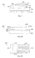
- FIG. 1 illustrates a side view of a MEMS switch according to an embodiment of the invention
- FIG. 2A illustrates a side view of a MEMS switch according to another embodiment of the invention
- FIG. 2B illustrates a top down view of the MEMS switch of FIG. 2A ;
- FIG. 2C illustrates a side view of the MEMS switch of FIGS. 2A-2B and operation of the same;
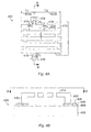
- FIG. 3A illustrates a top down view of a MEMS switch according to another embodiment of the invention
- FIG. 3B illustrates a cross-section view of the MEMS switch of FIG. 3A along line A to A';
- FIG. 4A illustrates a top down view of a MEMS switch according to another embodiment of the invention.
- FIG. 4B illustrates a cross-section view of the MEMS switch of FIG. 4A along line B to B'.
- the invention relates to microelectromechanical systems, and more particularly, to MEMS switches using magnetic actuation.
- the MEMS switch may be actuated with no internal power consumption. That is, the switch may be actuated with an external magnetic field.
- the switch is formed in an integrated solid state MEMS technology.
- the MEMS switch is formed on the micron or nanoscale and very reliable and accurate.
- the MEMS switch can be designed into various architectures, e.g., a cantilever architecture and torsion architecture.
- the torsion architecture is more efficient than a cantilever architecture.
- a MEMS switch is formed on a substrate.
- the substrate may be a silicon on insulator (SOI) substrate, glass substrate, silicon (Si) substrate, plastic substrate, and the like. Other substrates may also be used.
- the substrate may include insulating material.
- the insulating material may be formed into a thin insulator layer.
- the insulating material may be a dielectric layer, e.g., SiO 2 , SiN and the like.
- An input contact and output contact are formed on the substrate.
- the input contact provides input to the MEMS switch and the output contact provides output to the MEMS switch.
- a movable structure is supported over at least a portion of the substrate.
- the support location of the movable structure depends on whether the MEMS switch is a cantilever architecture or torsion architecture.
- the movable structure includes a proximal end portion, an intermediate portion and a distal end portion.
- the movable structure is supported with at least one of the proximal end portion or intermediate portion.
- the proximal end portion support is utilized in the cantilever architecture while the intermediate portion is utilized in the torsion architercture.
- an electrical contact can be formed on the distal end portion of the mov
- the movable structure is capable of actuation upon application of an external magnetic field. That is, the movable structure moves in order to provide electrical connection between the input contact and output contact through at least a portion of the movable structure.
- the input contact and output contact can be switched throughout such that the input is the output and vice versa. This is clearly within the scope of one of ordinary skill in the art.
- the movable structure may be configured into a plurality of different geometric configurations.
- the movable structure may be configured into a beam and formed with a support structure.
- the movable structure is formed on a support structure.
- the support structure is formed of conductive and/or magnetic material.
- the conductive material may be an alloy or pure material, e.g., gold, copper, and the like.
- the movable structure may be formed on the support structure and include a plurality of thin film magnetic material.
- the thin film magnetic material comprises magnetic material such as an alloy.
- the alloy includes NiFe, CoNi, and the like.
- the thin film may be formed with deposition techniques as known in the art such as chemical deposition process, physical deposition process, and the like. In a preferred embodiment, the thin film is deposited with electrical plating process.
- the thin film magnetic material may be deposited into interconnected strips on top of another structure or may independently form its own structure.
- the arrangement of thin film into long narrow strips minimizes demagnetization effect.
- the strips can be formed to have a width ranging from about 1 ⁇ m to about 1000 ⁇ m length ranging from about 10 ⁇ m to about 1000 ⁇ m and a height ranging from about 0.1 ⁇ m to about 100 ⁇ m.
- the aspect ratio of length/width, length/height, and width/height is greater than 1. In a preferred embodiment, the aspect ratio is not less than 5.
- the actuation of the switch is achieved by placing the MEMS switch into a magnetic field.
- the actuation may be achieved without the application of electrical power to the MEMS switch.
- the MEMS switch may be used to transmit information to other electrically connected circuits or devices coupled to the MEMS switch.
- the magnetic field may be passive, active or a combination of passive and active.
- An active magnetic field is generated with coils, e.g., in-plane spiral coil, multilevel meander magnetic core, and the like.
- a passive magnetic field is generated with a permanent magnet, e.g., Neodymium Iron Boron (NdFeB) magnet, samarium cobalt (SmCo) magnet, and the like.
- FIG. 1 illustrates a side view of a MEMS switch according to an embodiment of the invention.
- the MEMS switch is generally depicted as reference number 100.
- the MEMS switch 100 is formed on a substrate 102 such as silicon, glass, and the like.
- An input contact 104 of the switch is formed on the substrate 102.
- An output contact 106 is formed on the substrate 102.
- the input and output contacts are formed with electrically conductive material or an alloy of the same, e.g., gold or gold-alloy.
- the input contact and output contacts are electrically connected to other circuits (not shown) and devices (not shown) formed on said substrate.
- a movable structure 110 is coupled to a flexure 108.
- the flexure 108 is electrically coupled to the input contact 104 and designed to permit movement of the movable structure from a first position (A) to a second position (B) upon application of an external force.
- the first position (A) is an open position for the switch and the second position (B) is a closed position for the switch.
- the flexure 108 permits the structure to return to the first position (A) after application of the external force.
- the movable structure 110 includes a magnetic material such as NiFe, CoNi, and the like.
- the movable structure 110 includes additional material 112 formed on the movable structure 110 to balance stress.
- an electrical contact 114 may be formed on the structure 110.
- an external magnetic field 116 is applied to the MEMS switch 100.
- the movable structure 110 moves from a first position (A) (open) to a second position (B) (closed) permitting contact of at least a portion of the structure 110 with the output 106, thereby permitting an electrical current to travel from the input contact 104 to the output contact 106.
- the external magnetic field may be passive, active or a combination of the same.
- FIG. 2A illustrates a side view of a MEMS switch according to another embodiment of the invention.
- FIG. 2B illustrates a top down view of the MEMS switch of FIG. 2A .
- the MEMS switch is generally depicted as reference number 200.
- the MEMS switch 200 is formed on a substrate 202.
- the substrate includes silicon.
- An insulating layer 204 e.g. SiO 2 SiN and the like, is formed on the substrate 202.
- An input contact 206 and output contact 208 are formed on the insulating layer 204.
- the input and output contacts are formed of a conductive material, e.g. gold or gold alloy.
- a support member 210 having a predetermined geometry, e.g., post, is formed on the input contact 206.
- the movable structure 212 is formed on the support member 210.
- the movable structure 212 includes a support structure 214 and magnetic material 216 formed on the support structure.
- the movable structure 212 includes cantilever architecture having two or more beams 218 on the support structure 214.
- the support structure 214 is formed of gold having a thickness ranging from about 0.1 ⁇ m to about 5 ⁇ m.
- a magnetic material 216 is formed of NiFe thin film strips. The strips are formed to have a height of about 0.1 ⁇ m to about 100 ⁇ m. Patterning of the magnetic material into long narrow strips reduces the demagnetization filed along the direction of the long axis. That is, the application of an external magnetic field results in magnetic charges on the surface of the magnetic strips. The magnetic charges create a magnetic field in opposition to the applied external field in the strips.
- the demagnetization field is strongest in the smallest dimension of the strip and weakest in the largest dimension of the strip. The reason is due to the separation of the magnetic poles: the further apart between these magnetic surface charges, the less the interaction and the weaker the demagnetizing field. Therefore, when the aspect ratio of a strip is large (i.e. L>w>>h ), the magnetization primarily aligns in the direction of L . Much smaller components of the magnetization also exit along the directions of w and h , but can be neglected due to the large demagnetization field in these directions.
- additional layers may be formed on the plate (not shown), e.g., a gold layer, to reduce thermal-induced bending.
- the contact of the switch is open as shown in FIG. 2A .
- an external magnetic field 220 is applied via a magnetic source 222
- the movable structure 212 moves by magnetic torque created by the interaction of the magnetic material 216 permitting contact of at least a portion of the support structure 214 with the output contact 208, thereby permitting an electrical current to travel from the input contact 206 to the output contact 208.
- the structure returns to the open position.
- FIG. 3A illustrates a top down view of a MEMS switch according to another embodiment of the invention.
- FIG. 3B illustrates a cross-section view of the MEMS switch of FIG. 3A along line A to A'.
- the MEMS switch is generally depicted as reference number 300.
- the MEMS switch 300 is formed on a substrate 302 such as silicon (Si).
- An insulating layer 304 is formed on the substrate 302.
- the insulating layer 302 may be a dielectric layer, e. g., SiO 2 , SiN and the like.
- An input contact 310 and output contact 311 are formed on the adhesive layer 306, 308.
- a movable structure 314 is formed on the support structure 312.
- the movable structure 314 may be formed into a number of different geometric configurations to permit flexure of the beam and/or minimize demagnetization effects.
- the movable structure 314 is formed into a beam configuration of NiFe thin film strips.
- the support structure 314 has two beams 314a, 314b spaced apart and attached to the support structure 312. These beams 314a, 314b, have a length (Lb) of ranging from about 10 ⁇ m to about 300 ⁇ m and a width (Wb) ranging from about 1 ⁇ m to about 100 ⁇ m. These beams 314a, 314b, provide stiffness to the movable structure 314.
- the movable structure 314 has a main portion 314c having a length (Lm) ranging from about 100 ⁇ m to about 5000 ⁇ m or more. Preferably, the length (Lm) is about 300 ⁇ m to 1000 ⁇ m.
- the main portion 314c of the movable structure 314 is formed into a plurality of strips each having a width (Ws) ranging from about 10 ⁇ m to 500 ⁇ m and an empty space (Ss) ranging from about 1 ⁇ m to about 50 ⁇ m.
- the strips are connected with various connectors 316 as shown in FIG. 3B .
- a contact 318 is formed on an end portion of the movable structure 314.
- the contact is formed from a conductive material, e.g., gold.
- FIG. 4A illustrates a top down view of a MEMS switch according to another embodiment of the invention.
- FIG. 4B illustrates a cross-section view of the MEMS switch of FIG. 4A along line B to B'.
- the MEMS switch is generally depicted as reference number 400.
- the MEMS switch 400 is formed on a Si substrate 402.
- An insulating layer 404 is formed on the substrate 402.
- the insulating layer 404 may be a dielectric layer, e.g., SiO 2 , SiN and the like.
- An adhesive layer 406, including titanium, chromium and the like, is formed on at least a portion of the insulating layer 404.
- Input contacts 408 are formed on the substrate 402. In this embodiment, there are two input contacts 408; these contacts are made with gold.
- the input contacts have a thickness of about 5000 ⁇ .
- the MEMS switch 400 is configured to have torsion architecture.
- a first structure 410 and second structure 412 is formed in contact with the input contacts.
- a movable structure 414 is coupled to the first structure 410 and second structure 412 in an intermediate portion of the movable structure 414.
- the movable structure 414 is coupled to a first torsion bar 416 and second torsion bar 418.
- the torsion bars 416, 418 have a width (Wt) of in the range from about 1 ⁇ m to about 100 ⁇ m and a length (Lt) in the range from about 10 ⁇ m to about 500 ⁇ m.
- the movable structure 414 has a predetermined geometry with a plurality of openings 420 formed with a plurality of interconnected thin magnetic film strips.
- the magnetic strips 422 are now described in two different sections: a first section 422a leading to the torsion bars 416, 418 and a second section going from the torsion bars 416, 418 towards an opposite end of the magnetic strip 422.
- the first section 422a has a length (L1) ranging from about 50 ⁇ m to about 1000 ⁇ m and a width (W b1 ) ranging from about of about 10 ⁇ m to about 500 ⁇ m.
- the second section 422b has a length (L2) ranging from about 50 to about 1000 ⁇ m and a width (Wb2) ranging from about 10 to about 500 ⁇ m.
- the first and second sections have a uniform thickness ranging from about 1 ⁇ m to about 100 ⁇ m.
- the spacing between the magnetic strips 422 may range from of about 1 ⁇ m to 50 ⁇ m.
- the magnetic strips are formed from NiFe, CoFe and the like.
- an additional layer e.g., conductive or magnetic may, be deposited on top of the strips 422 in order to balance the stresses.
- the movable structure 414 utilizes the torsion bars 416, 418 to rotate the movable structure upon an application of an external magnetic field (not shown).
- This embodiment has a high sensitivity to an external magnetic field as compared to the cantilever architecture. Compared to a cantilever architecture with magnetic strips of the same length, torsion architecture can achieve higher sensitivity due to its larger rotation angle.
Landscapes
- Physics & Mathematics (AREA)
- Electromagnetism (AREA)
- Micromachines (AREA)
Applications Claiming Priority (2)
| Application Number | Priority Date | Filing Date | Title |
|---|---|---|---|
| US14257209P | 2009-01-05 | 2009-01-05 | |
| US12/475,392 US8174342B2 (en) | 2009-01-05 | 2009-05-29 | Microelectromechanical system |
Publications (2)
| Publication Number | Publication Date |
|---|---|
| EP2204831A2 true EP2204831A2 (de) | 2010-07-07 |
| EP2204831A3 EP2204831A3 (de) | 2013-12-25 |
Family
ID=41796121
Family Applications (1)
| Application Number | Title | Priority Date | Filing Date |
|---|---|---|---|
| EP20100150053 Withdrawn EP2204831A3 (de) | 2009-01-05 | 2010-01-04 | Mikroelektromechanisches System |
Country Status (3)
| Country | Link |
|---|---|
| US (1) | US8174342B2 (de) |
| EP (1) | EP2204831A3 (de) |
| CN (2) | CN101794678A (de) |
Cited By (1)
| Publication number | Priority date | Publication date | Assignee | Title |
|---|---|---|---|---|
| CN105632843A (zh) * | 2014-11-26 | 2016-06-01 | 中国科学院宁波材料技术与工程研究所 | 一种三维微/纳机电开关及其制备方法 |
Families Citing this family (14)
| Publication number | Priority date | Publication date | Assignee | Title |
|---|---|---|---|---|
| US8608085B2 (en) * | 2010-10-15 | 2013-12-17 | Nanolab, Inc. | Multi-pole switch structure, method of making same, and method of operating same |
| US8797127B2 (en) | 2010-11-22 | 2014-08-05 | Taiwan Semiconductor Manufacturing Company, Ltd. | MEMS switch with reduced dielectric charging effect |
| CN102543591B (zh) * | 2010-12-27 | 2014-03-19 | 上海丽恒光微电子科技有限公司 | Mems开关及其制作方法 |
| FR2970596B1 (fr) * | 2011-01-19 | 2013-02-08 | Commissariat Energie Atomique | Contacteur et interrupteur |
| US9225311B2 (en) * | 2012-02-21 | 2015-12-29 | International Business Machines Corporation | Method of manufacturing switchable filters |
| SG2012068896A (en) * | 2012-09-17 | 2014-04-28 | Schneider Electric South East Asia Hq Pte Ltd | Tool and method for switching an electromagnetic relay |
| CN106573770B (zh) * | 2014-06-27 | 2019-08-06 | 英特尔公司 | 用于静摩擦补偿的磁性纳米机械器件 |
| RU167556U1 (ru) * | 2016-05-31 | 2017-01-10 | Федеральное государственное бюджетное образовательное учреждение высшего образования "Рязанский государственный радиотехнический университет" | Планарный магнитоуправляемый коммутатор |
| CN106206161A (zh) * | 2016-06-29 | 2016-12-07 | 北京大学 | 一种基于洛伦兹力的新型离面mems开关 |
| US10529518B2 (en) * | 2016-09-19 | 2020-01-07 | Analog Devices Global | Protection schemes for MEMS switch devices |
| US10825628B2 (en) | 2017-07-17 | 2020-11-03 | Analog Devices Global Unlimited Company | Electromagnetically actuated microelectromechanical switch |
| US11652425B2 (en) * | 2017-12-22 | 2023-05-16 | MEMS Drive (Nanjing) Co., Ltd. | MEMS actuation system |
| JP6950613B2 (ja) | 2018-04-11 | 2021-10-13 | Tdk株式会社 | 磁気作動型memsスイッチ |
| CN112909451B (zh) * | 2021-01-11 | 2021-10-19 | 陕西索飞电子科技有限公司 | 一种手自一体式波导微波开关结构 |
Citations (2)
| Publication number | Priority date | Publication date | Assignee | Title |
|---|---|---|---|---|
| US4570139A (en) * | 1984-12-14 | 1986-02-11 | Eaton Corporation | Thin-film magnetically operated micromechanical electric switching device |
| EP1953116A2 (de) * | 2007-02-05 | 2008-08-06 | Commissariat A L'energie Atomique | Bedienungsmikrosystem und dessen Herstellungsverfahren |
Family Cites Families (4)
| Publication number | Priority date | Publication date | Assignee | Title |
|---|---|---|---|---|
| CA2211830C (en) * | 1997-08-22 | 2002-08-13 | Cindy Xing Qiu | Miniature electromagnetic microwave switches and switch arrays |
| US6496612B1 (en) * | 1999-09-23 | 2002-12-17 | Arizona State University | Electronically latching micro-magnetic switches and method of operating same |
| US6794965B2 (en) * | 2001-01-18 | 2004-09-21 | Arizona State University | Micro-magnetic latching switch with relaxed permanent magnet alignment requirements |
| US6633158B1 (en) * | 2001-09-17 | 2003-10-14 | Jun Shen | Micro magnetic proximity sensor apparatus and sensing method |
-
2009
- 2009-05-29 US US12/475,392 patent/US8174342B2/en active Active
-
2010
- 2010-01-04 EP EP20100150053 patent/EP2204831A3/de not_active Withdrawn
- 2010-01-05 CN CN201010002305.8A patent/CN101794678A/zh active Pending
- 2010-01-05 CN CN201610262766.6A patent/CN105679607A/zh active Pending
Patent Citations (2)
| Publication number | Priority date | Publication date | Assignee | Title |
|---|---|---|---|---|
| US4570139A (en) * | 1984-12-14 | 1986-02-11 | Eaton Corporation | Thin-film magnetically operated micromechanical electric switching device |
| EP1953116A2 (de) * | 2007-02-05 | 2008-08-06 | Commissariat A L'energie Atomique | Bedienungsmikrosystem und dessen Herstellungsverfahren |
Cited By (2)
| Publication number | Priority date | Publication date | Assignee | Title |
|---|---|---|---|---|
| CN105632843A (zh) * | 2014-11-26 | 2016-06-01 | 中国科学院宁波材料技术与工程研究所 | 一种三维微/纳机电开关及其制备方法 |
| CN105632843B (zh) * | 2014-11-26 | 2018-06-26 | 中国科学院宁波材料技术与工程研究所 | 一种三维微/纳机电开关及其制备方法 |
Also Published As
| Publication number | Publication date |
|---|---|
| CN105679607A (zh) | 2016-06-15 |
| US8174342B2 (en) | 2012-05-08 |
| US20100171575A1 (en) | 2010-07-08 |
| EP2204831A3 (de) | 2013-12-25 |
| CN101794678A (zh) | 2010-08-04 |
Similar Documents
| Publication | Publication Date | Title |
|---|---|---|
| US8174342B2 (en) | Microelectromechanical system | |
| Niarchos | Magnetic MEMS: key issues and some applications | |
| US6469603B1 (en) | Electronically switching latching micro-magnetic relay and method of operating same | |
| US7215229B2 (en) | Laminated relays with multiple flexible contacts | |
| US6366186B1 (en) | Mems magnetically actuated switches and associated switching arrays | |
| US7642885B2 (en) | Electromechanical latching relay and method of operating same | |
| KR100632458B1 (ko) | 가속도 센서 | |
| JPH09198983A (ja) | 小型デバイス | |
| JPH0856025A (ja) | 自己バイアス多層磁気抵抗センサ | |
| US20060049900A1 (en) | Micro-magnetic latching switches with a three-dimensional solenoid coil | |
| US8143978B2 (en) | Electromechanical relay and method of operating same | |
| US8174343B2 (en) | Electromechanical relay and method of making same | |
| US7420447B2 (en) | Latching micro-magnetic switch with improved thermal reliability | |
| US20090243772A1 (en) | Bistable magnetic nanoswitch | |
| US8068002B2 (en) | Coupled electromechanical relay and method of operating same | |
| JP5727908B2 (ja) | 磁気メモリ素子 | |
| US20100231333A1 (en) | Electromechanical relay and method of making same | |
| US7253710B2 (en) | Latching micro-magnetic switch array | |
| JP2011060766A (ja) | 相互嵌合電極を備えた電気機械アクチュエータ | |
| US20020196112A1 (en) | Electronically switching latching micro-magnetic relay and method of operating same | |
| JP5066603B2 (ja) | 磁気センサ、及び磁気エンコーダ、ならびに磁気センサの製造方法 | |
| US6713908B1 (en) | Using a micromachined magnetostatic relay in commutating a DC motor | |
| Arnold et al. | Fabrication of microscale rotating magnetic machines |
Legal Events
| Date | Code | Title | Description |
|---|---|---|---|
| PUAI | Public reference made under article 153(3) epc to a published international application that has entered the european phase |
Free format text: ORIGINAL CODE: 0009012 |
|
| AK | Designated contracting states |
Kind code of ref document: A2 Designated state(s): AT BE BG CH CY CZ DE DK EE ES FI FR GB GR HR HU IE IS IT LI LT LU LV MC MK MT NL NO PL PT RO SE SI SK SM TR |
|
| AX | Request for extension of the european patent |
Extension state: AL BA RS |
|
| RIN1 | Information on inventor provided before grant (corrected) |
Inventor name: MIN, TANG Inventor name: ITALIA, FRANCESCO Inventor name: NOVIELLO, GIUSEPPE Inventor name: LIAO, EBIN |
|
| PUAL | Search report despatched |
Free format text: ORIGINAL CODE: 0009013 |
|
| AK | Designated contracting states |
Kind code of ref document: A3 Designated state(s): AT BE BG CH CY CZ DE DK EE ES FI FR GB GR HR HU IE IS IT LI LT LU LV MC MK MT NL NO PL PT RO SE SI SK SM TR |
|
| AX | Request for extension of the european patent |
Extension state: AL BA RS |
|
| RIC1 | Information provided on ipc code assigned before grant |
Ipc: H01H 50/00 20060101AFI20131121BHEP |
|
| 17P | Request for examination filed |
Effective date: 20140625 |
|
| RBV | Designated contracting states (corrected) |
Designated state(s): AT BE BG CH CY CZ DE DK EE ES FI FR GB GR HR HU IE IS IT LI LT LU LV MC MK MT NL NO PL PT RO SE SI SK SM TR |
|
| 17Q | First examination report despatched |
Effective date: 20150316 |
|
| STAA | Information on the status of an ep patent application or granted ep patent |
Free format text: STATUS: EXAMINATION IS IN PROGRESS |
|
| STAA | Information on the status of an ep patent application or granted ep patent |
Free format text: STATUS: THE APPLICATION IS DEEMED TO BE WITHDRAWN |
|
| 18D | Application deemed to be withdrawn |
Effective date: 20171121 |