EP2199854B1 - Hybrid polymer mold for nano-imprinting and method for making the same - Google Patents
Hybrid polymer mold for nano-imprinting and method for making the same Download PDFInfo
- Publication number
- EP2199854B1 EP2199854B1 EP08172338.9A EP08172338A EP2199854B1 EP 2199854 B1 EP2199854 B1 EP 2199854B1 EP 08172338 A EP08172338 A EP 08172338A EP 2199854 B1 EP2199854 B1 EP 2199854B1
- Authority
- EP
- European Patent Office
- Prior art keywords
- resist
- polymer mold
- polymer
- chemical composition
- mold
- Prior art date
- Legal status (The legal status is an assumption and is not a legal conclusion. Google has not performed a legal analysis and makes no representation as to the accuracy of the status listed.)
- Active
Links
- 229920000642 polymer Polymers 0.000 title claims description 45
- 238000000034 method Methods 0.000 title claims description 40
- 239000000203 mixture Substances 0.000 claims description 59
- 230000008569 process Effects 0.000 claims description 33
- NIXOWILDQLNWCW-UHFFFAOYSA-M Acrylate Chemical compound [O-]C(=O)C=C NIXOWILDQLNWCW-UHFFFAOYSA-M 0.000 claims description 26
- 239000000126 substance Substances 0.000 claims description 19
- 230000005855 radiation Effects 0.000 claims description 13
- 150000002118 epoxides Chemical class 0.000 claims description 10
- 238000006116 polymerization reaction Methods 0.000 claims description 10
- QYKIQEUNHZKYBP-UHFFFAOYSA-N Vinyl ether Chemical class C=COC=C QYKIQEUNHZKYBP-UHFFFAOYSA-N 0.000 claims description 9
- 239000000178 monomer Substances 0.000 claims description 9
- JOYRKODLDBILNP-UHFFFAOYSA-N Ethyl urethane Chemical compound CCOC(N)=O JOYRKODLDBILNP-UHFFFAOYSA-N 0.000 claims description 8
- 150000001875 compounds Chemical class 0.000 claims description 6
- 230000001747 exhibiting effect Effects 0.000 claims description 5
- 125000001931 aliphatic group Chemical group 0.000 claims description 4
- 239000012952 cationic photoinitiator Substances 0.000 claims description 4
- 239000012949 free radical photoinitiator Substances 0.000 claims description 4
- 229920001577 copolymer Polymers 0.000 claims description 3
- 239000003999 initiator Substances 0.000 claims description 3
- CERQOIWHTDAKMF-UHFFFAOYSA-M Methacrylate Chemical compound CC(=C)C([O-])=O CERQOIWHTDAKMF-UHFFFAOYSA-M 0.000 claims description 2
- 239000003054 catalyst Substances 0.000 claims description 2
- 239000000758 substrate Substances 0.000 description 59
- 239000000463 material Substances 0.000 description 30
- 239000004094 surface-active agent Substances 0.000 description 28
- PXHVJJICTQNCMI-UHFFFAOYSA-N nickel Substances [Ni] PXHVJJICTQNCMI-UHFFFAOYSA-N 0.000 description 22
- 239000010410 layer Substances 0.000 description 20
- 238000009472 formulation Methods 0.000 description 18
- 239000010408 film Substances 0.000 description 14
- LYCAIKOWRPUZTN-UHFFFAOYSA-N Ethylene glycol Chemical compound OCCO LYCAIKOWRPUZTN-UHFFFAOYSA-N 0.000 description 12
- 150000001252 acrylic acid derivatives Chemical class 0.000 description 11
- 238000001723 curing Methods 0.000 description 10
- 239000006185 dispersion Substances 0.000 description 7
- 239000007788 liquid Substances 0.000 description 7
- XLYOFNOQVPJJNP-UHFFFAOYSA-N water Substances O XLYOFNOQVPJJNP-UHFFFAOYSA-N 0.000 description 7
- 229910052710 silicon Inorganic materials 0.000 description 6
- XUIMIQQOPSSXEZ-UHFFFAOYSA-N Silicon Chemical compound [Si] XUIMIQQOPSSXEZ-UHFFFAOYSA-N 0.000 description 5
- 239000002318 adhesion promoter Substances 0.000 description 5
- 229920001400 block copolymer Polymers 0.000 description 5
- 238000005259 measurement Methods 0.000 description 5
- -1 polyethylene terephthalate Polymers 0.000 description 5
- 229920006254 polymer film Polymers 0.000 description 5
- 239000002861 polymer material Substances 0.000 description 5
- 239000010703 silicon Substances 0.000 description 5
- 229940043375 1,5-pentanediol Drugs 0.000 description 4
- ALQSHHUCVQOPAS-UHFFFAOYSA-N Pentane-1,5-diol Chemical compound OCCCCCO ALQSHHUCVQOPAS-UHFFFAOYSA-N 0.000 description 4
- NZZFYRREKKOMAT-UHFFFAOYSA-N diiodomethane Chemical compound ICI NZZFYRREKKOMAT-UHFFFAOYSA-N 0.000 description 4
- 229920005570 flexible polymer Polymers 0.000 description 4
- 239000002184 metal Substances 0.000 description 4
- 229910052751 metal Inorganic materials 0.000 description 4
- 238000001127 nanoimprint lithography Methods 0.000 description 4
- 230000035515 penetration Effects 0.000 description 4
- 239000010702 perfluoropolyether Substances 0.000 description 4
- QVGXLLKOCUKJST-UHFFFAOYSA-N atomic oxygen Chemical compound [O] QVGXLLKOCUKJST-UHFFFAOYSA-N 0.000 description 3
- 230000015572 biosynthetic process Effects 0.000 description 3
- 238000006243 chemical reaction Methods 0.000 description 3
- 230000007246 mechanism Effects 0.000 description 3
- 239000001301 oxygen Substances 0.000 description 3
- 229910052760 oxygen Inorganic materials 0.000 description 3
- 239000012071 phase Substances 0.000 description 3
- 239000010453 quartz Substances 0.000 description 3
- 230000010076 replication Effects 0.000 description 3
- VYPSYNLAJGMNEJ-UHFFFAOYSA-N silicon dioxide Inorganic materials O=[Si]=O VYPSYNLAJGMNEJ-UHFFFAOYSA-N 0.000 description 3
- 239000007787 solid Substances 0.000 description 3
- 238000003786 synthesis reaction Methods 0.000 description 3
- 235000012431 wafers Nutrition 0.000 description 3
- 238000009736 wetting Methods 0.000 description 3
- 239000004593 Epoxy Substances 0.000 description 2
- AHGFXGSMYLFWEC-UHFFFAOYSA-N [SiH4].CC(=C)C(O)=O Chemical class [SiH4].CC(=C)C(O)=O AHGFXGSMYLFWEC-UHFFFAOYSA-N 0.000 description 2
- 229910045601 alloy Inorganic materials 0.000 description 2
- 239000000956 alloy Substances 0.000 description 2
- 125000002091 cationic group Chemical group 0.000 description 2
- 238000009792 diffusion process Methods 0.000 description 2
- 238000005516 engineering process Methods 0.000 description 2
- 238000010438 heat treatment Methods 0.000 description 2
- 230000000977 initiatory effect Effects 0.000 description 2
- 229910052759 nickel Inorganic materials 0.000 description 2
- 229920003023 plastic Polymers 0.000 description 2
- 239000004033 plastic Substances 0.000 description 2
- 229920003229 poly(methyl methacrylate) Polymers 0.000 description 2
- 229920006289 polycarbonate film Polymers 0.000 description 2
- 229920000139 polyethylene terephthalate Polymers 0.000 description 2
- 239000005020 polyethylene terephthalate Substances 0.000 description 2
- 239000004926 polymethyl methacrylate Substances 0.000 description 2
- 239000011148 porous material Substances 0.000 description 2
- 239000011342 resin composition Substances 0.000 description 2
- 238000005204 segregation Methods 0.000 description 2
- 239000000243 solution Substances 0.000 description 2
- 238000004528 spin coating Methods 0.000 description 2
- 239000010936 titanium Substances 0.000 description 2
- 229910052719 titanium Inorganic materials 0.000 description 2
- 238000012546 transfer Methods 0.000 description 2
- 206010073306 Exposure to radiation Diseases 0.000 description 1
- YCKRFDGAMUMZLT-UHFFFAOYSA-N Fluorine atom Chemical compound [F] YCKRFDGAMUMZLT-UHFFFAOYSA-N 0.000 description 1
- RTAQQCXQSZGOHL-UHFFFAOYSA-N Titanium Chemical compound [Ti] RTAQQCXQSZGOHL-UHFFFAOYSA-N 0.000 description 1
- MWGMEGAYPPQWFG-UHFFFAOYSA-N [SiH4].OC(=O)C=C Chemical compound [SiH4].OC(=O)C=C MWGMEGAYPPQWFG-UHFFFAOYSA-N 0.000 description 1
- 238000002835 absorbance Methods 0.000 description 1
- 239000000853 adhesive Substances 0.000 description 1
- 230000001070 adhesive effect Effects 0.000 description 1
- 229910052782 aluminium Inorganic materials 0.000 description 1
- XAGFODPZIPBFFR-UHFFFAOYSA-N aluminium Chemical compound [Al] XAGFODPZIPBFFR-UHFFFAOYSA-N 0.000 description 1
- 230000000712 assembly Effects 0.000 description 1
- 238000000429 assembly Methods 0.000 description 1
- 238000000089 atomic force micrograph Methods 0.000 description 1
- 239000003575 carbonaceous material Substances 0.000 description 1
- 230000008859 change Effects 0.000 description 1
- 238000012512 characterization method Methods 0.000 description 1
- 238000004140 cleaning Methods 0.000 description 1
- 239000011248 coating agent Substances 0.000 description 1
- 238000000576 coating method Methods 0.000 description 1
- 239000000084 colloidal system Substances 0.000 description 1
- 230000008602 contraction Effects 0.000 description 1
- 238000001816 cooling Methods 0.000 description 1
- 238000004132 cross linking Methods 0.000 description 1
- 230000000694 effects Effects 0.000 description 1
- 230000009881 electrostatic interaction Effects 0.000 description 1
- 239000003822 epoxy resin Substances 0.000 description 1
- 238000005530 etching Methods 0.000 description 1
- 238000002474 experimental method Methods 0.000 description 1
- 238000001125 extrusion Methods 0.000 description 1
- 229910052731 fluorine Inorganic materials 0.000 description 1
- 239000011737 fluorine Substances 0.000 description 1
- NBVXSUQYWXRMNV-UHFFFAOYSA-N fluoromethane Chemical compound FC NBVXSUQYWXRMNV-UHFFFAOYSA-N 0.000 description 1
- 239000007789 gas Substances 0.000 description 1
- 239000011521 glass Substances 0.000 description 1
- 230000009477 glass transition Effects 0.000 description 1
- 230000005661 hydrophobic surface Effects 0.000 description 1
- 230000006872 improvement Effects 0.000 description 1
- 239000012535 impurity Substances 0.000 description 1
- 239000004615 ingredient Substances 0.000 description 1
- 238000001746 injection moulding Methods 0.000 description 1
- 239000007791 liquid phase Substances 0.000 description 1
- 229910044991 metal oxide Inorganic materials 0.000 description 1
- 150000004706 metal oxides Chemical class 0.000 description 1
- 150000002739 metals Chemical class 0.000 description 1
- 238000002156 mixing Methods 0.000 description 1
- 239000002086 nanomaterial Substances 0.000 description 1
- 239000012044 organic layer Substances 0.000 description 1
- 239000011368 organic material Substances 0.000 description 1
- 239000002245 particle Substances 0.000 description 1
- JZDGWLGMEGSUGH-UHFFFAOYSA-N phenyl-(2,4,6-trimethylbenzoyl)phosphinic acid Chemical compound CC1=CC(C)=CC(C)=C1C(=O)P(O)(=O)C1=CC=CC=C1 JZDGWLGMEGSUGH-UHFFFAOYSA-N 0.000 description 1
- 238000000016 photochemical curing Methods 0.000 description 1
- 239000000049 pigment Substances 0.000 description 1
- 238000009832 plasma treatment Methods 0.000 description 1
- 229920000058 polyacrylate Polymers 0.000 description 1
- 239000004417 polycarbonate Substances 0.000 description 1
- 229920000515 polycarbonate Polymers 0.000 description 1
- 229920000647 polyepoxide Polymers 0.000 description 1
- 239000011112 polyethylene naphthalate Substances 0.000 description 1
- 238000010094 polymer processing Methods 0.000 description 1
- 239000004814 polyurethane Substances 0.000 description 1
- 229920002635 polyurethane Polymers 0.000 description 1
- 238000003847 radiation curing Methods 0.000 description 1
- 150000003254 radicals Chemical class 0.000 description 1
- 230000009257 reactivity Effects 0.000 description 1
- 230000009467 reduction Effects 0.000 description 1
- 239000011347 resin Substances 0.000 description 1
- 229920005989 resin Polymers 0.000 description 1
- 239000002094 self assembled monolayer Substances 0.000 description 1
- 239000004065 semiconductor Substances 0.000 description 1
- 230000035945 sensitivity Effects 0.000 description 1
- 238000004088 simulation Methods 0.000 description 1
- 239000011343 solid material Substances 0.000 description 1
- 238000001179 sorption measurement Methods 0.000 description 1
- 239000002344 surface layer Substances 0.000 description 1
- 238000012360 testing method Methods 0.000 description 1
- 229920001187 thermosetting polymer Polymers 0.000 description 1
- 239000004634 thermosetting polymer Substances 0.000 description 1
- 239000010409 thin film Substances 0.000 description 1
- 125000005409 triarylsulfonium group Chemical group 0.000 description 1
- 239000000080 wetting agent Substances 0.000 description 1
Images

Classifications
-
- B—PERFORMING OPERATIONS; TRANSPORTING
- B29—WORKING OF PLASTICS; WORKING OF SUBSTANCES IN A PLASTIC STATE IN GENERAL
- B29C—SHAPING OR JOINING OF PLASTICS; SHAPING OF MATERIAL IN A PLASTIC STATE, NOT OTHERWISE PROVIDED FOR; AFTER-TREATMENT OF THE SHAPED PRODUCTS, e.g. REPAIRING
- B29C33/00—Moulds or cores; Details thereof or accessories therefor
- B29C33/38—Moulds or cores; Details thereof or accessories therefor characterised by the material or the manufacturing process
- B29C33/3842—Manufacturing moulds, e.g. shaping the mould surface by machining
- B29C33/3857—Manufacturing moulds, e.g. shaping the mould surface by machining by making impressions of one or more parts of models, e.g. shaped articles and including possible subsequent assembly of the parts
-
- B—PERFORMING OPERATIONS; TRANSPORTING
- B29—WORKING OF PLASTICS; WORKING OF SUBSTANCES IN A PLASTIC STATE IN GENERAL
- B29C—SHAPING OR JOINING OF PLASTICS; SHAPING OF MATERIAL IN A PLASTIC STATE, NOT OTHERWISE PROVIDED FOR; AFTER-TREATMENT OF THE SHAPED PRODUCTS, e.g. REPAIRING
- B29C59/00—Surface shaping of articles, e.g. embossing; Apparatus therefor
- B29C59/02—Surface shaping of articles, e.g. embossing; Apparatus therefor by mechanical means, e.g. pressing
- B29C59/022—Surface shaping of articles, e.g. embossing; Apparatus therefor by mechanical means, e.g. pressing characterised by the disposition or the configuration, e.g. dimensions, of the embossments or the shaping tools therefor
-
- B—PERFORMING OPERATIONS; TRANSPORTING
- B82—NANOTECHNOLOGY
- B82Y—SPECIFIC USES OR APPLICATIONS OF NANOSTRUCTURES; MEASUREMENT OR ANALYSIS OF NANOSTRUCTURES; MANUFACTURE OR TREATMENT OF NANOSTRUCTURES
- B82Y10/00—Nanotechnology for information processing, storage or transmission, e.g. quantum computing or single electron logic
-
- B—PERFORMING OPERATIONS; TRANSPORTING
- B82—NANOTECHNOLOGY
- B82Y—SPECIFIC USES OR APPLICATIONS OF NANOSTRUCTURES; MEASUREMENT OR ANALYSIS OF NANOSTRUCTURES; MANUFACTURE OR TREATMENT OF NANOSTRUCTURES
- B82Y40/00—Manufacture or treatment of nanostructures
-
- G—PHYSICS
- G03—PHOTOGRAPHY; CINEMATOGRAPHY; ANALOGOUS TECHNIQUES USING WAVES OTHER THAN OPTICAL WAVES; ELECTROGRAPHY; HOLOGRAPHY
- G03F—PHOTOMECHANICAL PRODUCTION OF TEXTURED OR PATTERNED SURFACES, e.g. FOR PRINTING, FOR PROCESSING OF SEMICONDUCTOR DEVICES; MATERIALS THEREFOR; ORIGINALS THEREFOR; APPARATUS SPECIALLY ADAPTED THEREFOR
- G03F7/00—Photomechanical, e.g. photolithographic, production of textured or patterned surfaces, e.g. printing surfaces; Materials therefor, e.g. comprising photoresists; Apparatus specially adapted therefor
- G03F7/0002—Lithographic processes using patterning methods other than those involving the exposure to radiation, e.g. by stamping
-
- Y—GENERAL TAGGING OF NEW TECHNOLOGICAL DEVELOPMENTS; GENERAL TAGGING OF CROSS-SECTIONAL TECHNOLOGIES SPANNING OVER SEVERAL SECTIONS OF THE IPC; TECHNICAL SUBJECTS COVERED BY FORMER USPC CROSS-REFERENCE ART COLLECTIONS [XRACs] AND DIGESTS
- Y10—TECHNICAL SUBJECTS COVERED BY FORMER USPC
- Y10T—TECHNICAL SUBJECTS COVERED BY FORMER US CLASSIFICATION
- Y10T428/00—Stock material or miscellaneous articles
- Y10T428/31504—Composite [nonstructural laminate]
- Y10T428/3154—Of fluorinated addition polymer from unsaturated monomers
Definitions
- the present invention relates to Nano-Imprinting in general and especially to the polymer mold with anti-sticking or anti-adhesion properties.
- nanoimprint lithography an inverted copy of the surface pattern of a template - often called a stamp - is transferred into an object, comprising a substrate and, applied thereto, a film of a moldable layer often called resist, e.g. a polymer material. After heating the object to a temperature above the glass transition temperature of the polymer film, the stamp is pressed towards the film, cooled and released from the stamp - often called demolding - to give a polymer film with the desired pattern. This process is defined as a "thermal imprint process”.
- a photo-resist material i.e. a resin composition, which cures upon exposure to photon radiation, covers the substrate.
- This so-called "Photon-imprint process” requires that either the substrate or the stamp is transparent.
- the object - comprising the substrate and the patterned polymer film - can be post-processed, e.g. by etching of the substrate within the imprinted regions to transfer the pattern to a target surface of the substrate.
- a method for transferring a pattern from a template to an object in an imprint process has been suggested, which involves a two-step process, which is described in JPA no. 2008-515059 , US patent application no. 11/450377 , US patent application no. 11/268574 and US patent application no. 11/305157 .
- the template or master used in an imprint process is generally a high cost product, and wear or damages to the template should therefore be minimized.
- the template may be made of any material, but is often made of Si, Ni, Ti, other metals, or quartz, optionally provided with an anti-stick layer.
- the object to be imprinted is often made of a relatively hard material, such as glass, quartz, a metal, a metal-oxide, silicon, or another semiconductor material, sometimes coated with different layers comprising metal, alloys, organic or carbonaceous materials. On their surfaces a comparatively soft moldable imprint layer is exposed.
- the imprinting of the object is a crucial moment, where parallel arrangement is important, and a very small residual layer of the moldable layer, often in the order of less than 10 nm, under the imprinted protruding structures is desired. Any non-parallel arrangement or excessive pressure may therefore cause damage to the template.
- the template will only be used against a polymer material, which is softer than the template material, thereby minimizing the risk of damage.
- the template and the substrate are not made of the same material, which they generally are not, they will typically have different thermal expansion coefficients. This means that during heating and cooling of the template and the substrate, the extent of expansion and contraction will be different. Even though the dimensional change is small, it may be devastating in an imprint process, since the features of the pattern to be transferred are in the order of micrometers or even nanometers. The result may therefore be reduced replication fidelity.
- stamp materials with low surface energies are for example known from US 2008/0000373 .
- Dae-Gem Choi et al., Langmuir, 2005, 21, 9390-9392 describes intermediate molds comprising a hybrid polymer material.
- a method for transferring a pattern from a template to an object in an imprint process involves a photon-based two-step process.
- a template having a structured surface is contacted with a polymer material to produce a flexible polymer replica having an inverse structured surface pattern of the template surface, herein referred to as an intermediate polymer stamp (IPS).
- IPS intermediate polymer stamp
- the IPS replica is used as a template in order to produce a second replica. It is coated with a moldable surface to give a replica displaying a pattern identical with the original template.
- the IPS is produced when a polymer carrier object coated with photo-polymerizable compounds, is pressed towards a template, deformed and cured with the STU TM process. After demolding, the patterned IPS will be applied as a new template to replicate its pattern in a photon based imprint process.
- 2-step imprint process are the anti-sticking or anti-adhesion properties of both the interfaces of the original template and the IPS resist as well as the cured and patterned IPS resist and the substrate resist.
- the material is coated on a polymer carrier object and used in an improved imprint process, having high replication fidelity, and which is easy and suitable to employ industrially.
- Table 1 displays results from contact angles measurements for water, 1,5-pentanediol, diiodomethane and ethylene glycol provided on different surfaces.
- Table 2 displays surface energies, together with their dispersion and polar contributions calculated from the contact angle results of table 1 applying the model of Owens, Wendt, Rabel and Kaelble. Additionally, the table contains the calculated work of adhesions and interface energies for different interfaces, calculated from the assorted surface energies contributions displayed in table 2 with the help of equations 2 and 4.
- the original stamp or template is usually equipped with an anti-sticking layer (i.e. a self assembling monolayer film) in order to decrease its surface energy, which is described in Japanese patent no. 3892460 in 2006 and US patent application no. 11/597570 .
- an anti-sticking layer i.e. a self assembling monolayer film
- High contact angles are usually observed for various liquids commonly employed in contact angle measurements, as illustrated in table 1. Especially for water the observed contact angles are higher than 100°, due to the high hydrophobicity of the anti-sticking treated surfaces.
- Fluorinated molecules or fluoro-surfactants have the characteristic of lowering the surface energy of a liquid phase efficiently even at low concentrations.
- the introduction of fluoro-surfactants into a composition comprising photo-reactive compounds can lower the surface energy by forming a concentrated fluorocarbon layer at the surface of the liquid.
- the stamp equipped with an anti-sticking layer will be pressed against a non-cured resist composition comprising fluoro-surfactants.
- the non-cured resist can be regarded as a liquid with high viscosity.
- the resist is deposited onto a polymer carrier object.
- polymer carrier object refers to a flexible, ductile, and transparent polymer specimen, comprising a thermoplast or a thermosetting polymer material. Typical materials are polycarbonate, polymethyl methacrylate (PMMA), polyethylene terephthalate (PET), and polyethylene naphthalate (PEN). Preferably, the polymer carrier object is homogenously made of one or more of these materials, but in an alternative embodiment the material may comprise other compounds as well.
- the polymer carrier object might be a thin polymer film fabricated in an extrusion process (typical thickness 50-200 micrometer) [Osswald] or a disk, fabricated with the help of an injection molding process (typical thickness 300 micrometer up to 1 millimeter).
- the work of adhesion can be regarded as the required work necessary to remove a liquid (e.g. resist) from a solid surface (e.g. stamp) (see e.g. [Adamson, Gast]).
- a liquid e.g. resist
- a solid surface e.g. stamp
- the work of adhesion W A of an interface (Eq. 2) comprising a stamp equipped with an anti-sticking layer and a resin composition comprising fluoro-surfactants is lower than that comprising an anti-sticking treated stamp and a resist without fluoro-surfactants, because in the first case both the stamp and the non-cured resist exhibit low surface energies, ⁇ stamp and ⁇ resist , and W A will be low even if the interface energy ⁇ stamp, resist is very small.
- the fluoro-surfactant containing resist will obtain a more pronounced wettability with the stamp (i.e. smaller contact angles will be observed) - compared to the non-fluorine-containing species because the fluoro-surfactants are reducing the surface energy of the resist- and additionally also the interface energy of the stamp resist interface - acting as a wetting agent.
- the better wetting leads to a more pronounced and faster penetration of the pattern of the stamp under the assumption that the viscosity of resist remains almost unchanged by the introduction of low concentrations of the fluoro-surfactants.
- the introduction of fluoro-surfactants has three advantages; first the increased pattern penetration enables both the reduction of the applied pressure between the stamp and the IPS in the imprint process, second is the decrease of the process time and third, the reduced surface energy that improves the wettability and - after curing - adhesion with impurity particles, resulting in a better cleaning effect of the stamp.
- Table 1 shows typical contact angles with water, 1,5-pentanediol, diiodomethane and ethylene glycol. Water contact angles higher than 100° could be observed for the different formulations after curing. Additionally, when the surface energy is divided into polar forces and dispersion forces, according to the model of Owens and Wendt, the surface energy ⁇ of the IPS is strongly dominated by the dispersion contribution ⁇ d whereas the polar contribution ⁇ p is very low due to the non-polarity of the fluoro-surfactants.
- Table 2 presents some parameters which are important for the characterization of different surfaces or interfaces of the stamp/ IPS, e.g. ⁇ , ⁇ d , ⁇ p , W A , ⁇ 1,2 .
- the different parameters have been calculated from contact angles measurements (table 1).
- the interfaces are characterized by low work of adhesions, W A , of approx. 30 mJ/m 2 and low interface energies, ⁇ 1,2 of almost 0 mJ/m 2 up to below 1 mJ/ m 2 .
- a low work of adhesion is very adventurous when a joint should exhibit low adhesion strength so that demolding can be performed easily.
- Low interface energies are found when the two surfaces establishing an interface are chemically very similar e.g. in their polarity. For example a joint consisting of two completely similar materials exhibits an interface energy of 0 mJ/m 2 .
- W B f W A ⁇ ⁇
- the IPS resist/ substrate resist interfaces are characterized by slightly higher values of W A (approx. 40 - 54 mJ/m 2 ) and also by higher values of ⁇ 1,2 (approx. 2 - 4 mJ/m 2 ).
- the higher values of ⁇ 1,2 can be interpreted that the two surfaces establishing the IPS resist/ substrate resist interfaces are chemically less "similar" than the two surfaces establishing the Ni stamp/ IPS resist interfaces.
- the pronounced mechanical interlocking leading to plastic deformation upon demolding
- W A is small, W B will be quite large.
- Another crucial parameter is diffusion between the non-cured substrate resists and the cured IPS resist if the cured resist is soluble in the components of the non-cured one. For pronounced anti-adhesion properties the cured resist should be insoluble in the non-cured resist. At least, electrostatic interactions between the IPS and the substrate resist could be minimized when the two surfaces do not exhibit opposite electronegativity characters, which would reduce ⁇ P of Equation [4] concerning the acid-base model of Fowkes [Pocius].
- Formulations containing mixtures of different mono- or multi-functionalized monomers and/ or oligomers, which after curing exhibits high degrees of crosslinking and low solubility, are applied as imprint materials.
- the acrylate based resists are characterized by high reactivity and polymerize rapidly in the presence of photogenerated free radicals and in the absence of oxygen at ambient temperature.
- the acrylate-based resists are for many reasons attractive material, but generally suffer from drawbacks such as high oxygen sensitivity and large shrinkage upon polymerization.
- Cationic induced polymerization of epoxides and vinyl ethers is comparatively slow, but offers several advantages such as good mechanical properties of the resist, low shrinkage, and an oxygen insensitive process.
- the present innovation describes how material properties from different polymers may be combined by blending proper ratios of interpenetrating polymer networks (IPNs) forming a hybrid polymer system comprising for example both acrylates and epoxides [Vabrik et al].
- IPPNs interpenetrating polymer networks
- the synthesis of IPNs is achieved by photoinitiated polymerization of monomers, which polymerize through different mechanisms, typically photoinitiated free radial mechanism and photoinitiated cationic mechanism.
- the developed IPS resist is a hybrid resist comprising both: acrylates and epoxides, or acrylates and vinyl ethers.
- Acrylate comprising hybrid resists are generally characterized by a fast curing of the acrylate monomers leading to a close to full conversion of the acrylates and lower conversions of the epoxides/vinyl ether.
- the high conversion of the acrylates circumvents polymerization of the remaining acrylates present close to the surface of the IPS resist and an acrylate-based substrate resist, which facilitates efficient demolding.
- the sequential polymerization is here presented as a promising technique for the improvement of material properties such as reduced polymer shrinkage, due to the low shrinkage of the epoxides, and higher imprint fidelity etc.
- the anti-sticking treatment of the IPS resist results in a low surface energy, necessary for enhanced release properties between in particular the IPS resist and the substrate resist.
- a low IPS surface energy leads to a low work of adhesion W A and - if the substrate resist is selected carefully - a high interfacial energy ⁇ 1,2 .
- One class of molecules that have showed strong potential as efficient fluoro-surfactants, with the ability to diffuse to the surface of the mold resist forming an anti-sticking layer, are perfluoropolyether (PFPE) based derivatives end terminated with one or several chemical functionalities, such as (meth)acrylates.
- PFPE perfluoropolyether
- the PFPE backbone has been linked to the (meth)acrylates via linear or branched aliphatic urethane block copolymers chain and is manufactured, which has the following structure: Y p -X-CF 2 CF 2 O(CF 2 F 2 O) m (CF 2 O) n CF 2 CF 2 -X-Y p , where X is an aliphatic urethane building block, Y is a (meth)acrylate and p equals one or two.
- the molecular weight of the PFPE part of the co-polymer is 1500-2000 g/mol and the ratio m/n is 1.5 to 2.5.
- the substrate resist may be a purely acrylate based resist, or a hybrid resist, with material properties combined from the two types of polymers, comprising acrylates and vinyl ethers, or acrylates and epoxides.
- Composition 1 is a purely acrylate-based IPS formulation containing approximately 0.25% by weight of the fluoro-surfactant Y-X-CF 2 CF 2 O(CF 2 F 2 O) m (CF 2 O) n CF 2 CF 2 -X-Y, where X is a short linear urethane block copolymers chain and Y is a methacrylate group.
- Composition 2 (referred to as "IPS70/95”) is an acrylate/epoxide-hybrid IPS formulation containing approximately 1% by weight of a fluoro-surfactant with the structure: where R is a chemical functionality with the ability to bind covalently to the IPS material upon curing, e.g. acrylate, x is an integer in a range of 0 to 7, inclusive; and y is an integer in a range of 0 to 15, inclusive.
- R is a chemical functionality with the ability to bind covalently to the IPS material upon curing, e.g. acrylate, x is an integer in a range of 0 to 7, inclusive; and y is an integer in a range of 0 to 15, inclusive.
- Composition 3 is an acrylate/epoxide-hybrid IPS formulation containing approximately 1% by weight of the fluoro-surfactant Y 2 -X-CF 2 CF 2 O(CF 2 F 2 O) m (CF 2 O) n CF 2 CF 2 -X-Y 2 , where X is a long branched urethane block copolymers chain and Y is an acrylate group.
- Composition 4 is an acrylate/epoxide-hybrid IPS formulation containing approximately 0.8% by weight of the fluoro-surfactant Y 2 -X-CF 2 CF 2 O(CF 2 F 2 O) m (CF 2 O) n CF 2 CF 2 -X-Y 2 , where X is a long branched urethane block copolymers chain and Y is an acrylate group, and 0.6% by weight of a fluoro-surfactant with the structure specified in IPS composition 2.
- Composition 5 is a purely acrylate-based IPS formulation containing approximately 1% by weight of the fluoro-surfactant Y 2 -X-CF 2 CF 2 O(CF 2 F 2 O) m (CF 2 O) n CF 2 CF 2 -X-Y 2 , where X is a long branched urethane block copolymers chain and Y is an acrylate group.
- Substrate resist 1 (referred to as "SR20/47”) is a purely acrylate-based substrate resist formulation without functionalized siloxanes.
- Substrate resist 2 compositions are a purely acrylate-based substrate resists formulations containing functionalized siloxanes.
- Substrate resist 3 compositions are a purely acrylate-based substrate resists formulations without functionalized siloxanes.
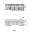
- the two material assemblies 1 and 14 as displayed in figures 1 a and 1b, respectively, can be regarded as the essential prerequisite to succeed the two-step process illustrated in figure 2 .
- the first step is illustrated in figs. 2a-2c and the second step in figs. 2d-2f .
- the stamp or template 10 composed of e.g. silicon, quartz, nickel or other metal such as aluminum or titanium, an alloy or even a polymer material has a patterned surface 9, comprising ribs, grooves, protrusions or recesses, having heights and widths in the order of micrometers or nanometers.
- the template surface 9 is equipped with an anti-adhesion layer 8.
- the template 10 is placed with the surface of the anti-adhesion layer 8 in a way facing and contacting a surface 6 of the specimen 1.
- a pressure between 1-40 bars is applied on the backsides of either the template 10 or the polymer carrier object 2 in order to press the template 10 and the specimen 1 together.
- the resist 5 will fill the cavities of the template surface 9, equipped with an anti-sticking layer 8. Additionally, the fluoro-surfactants will predominately settle at the surface 6 - now facing the template anti-sticking layer 8 - or within the surface-near region of the resist 5 in order to minimize the interface energy of the interface between the template anti-sticking layer 8 and the resist surface 6.
- the sandwich arrangement - consisting of a template 10 equipped with an anti-sticking layer 8, a polymer carrier object 2, and photo-polymerizable resist 5 and maybe an adhesion promoter 4 - is irradiated with ultraviolet light either through the backside of the template 10 or through the polymer carrier object 2 as displayed in fig 2b ).
- the template has to be transparent, whereas in the second case the polymer carrier object has to fulfill this requirement.
- the template 10 is separated or demolded from the flexible polymer replica 11 leaving a relief image on the surface 13 of the solidified photopolymer film 12, coated on the polymer carrier object 2 as displayed in Fig 2c .
- the flexible polymer replica 11 herein is referred to as an intermediate polymer stamp (IPS).
- the IPS 11 is used to transfer the pattern of its surface 13 to a target substrate as illustrated in Figs 2d) - 2f ).
- the surface 13 of the flexible polymer stamp 11 will be placed in contact with a surface 19 of an object 14 comprising a substrate 15 having a surface 16 covered by a thin moldable surface layer 18 of a non-cured photo curable resist.
- a thin organic layer 17 acting as an adhesion promoter might be placed in-between the substrate surface 16 and the resist 18.
- the IPS 11 and object 14 will be forced together and after applied exposure of the photo-curable resist 18 to radiation, the resist will be cured. After release an inversion of the pattern located on the surface 13 of the IPS 11 has been formed in the surface 22 of the layer 21, as shown in fig. 2f .
- the IPS 11 has to be transparent to the applied radiation or shows minor absorbance in order to transmit a sufficient amount of radiation necessary for curing the resist 18 upon exposure to radiation.
- IPS and substrate resist formulations which fulfill the requirement of this invention to provide materials for an improved imprint process, having high replication fidelity, and which is easy and suitable to employ industrially.
- the different formulations could easily be applied within the 2-step process - schematically described in figure 2 - without any further anti-sticking treatment of the IPS (surface 13 in figure 2c or 2d ), and thus avoids the need of an external process, as for example a plasma treatment, and/ or a coating of an additional thin film.
- Table 1 displays results for water, 1,5-pentanediol, diiodomethane and ethylene glycol applied to different surfaces.
- the contact angle measurements have been carried out with a Tracker contact-angle measurement instrument from Teclis.
- the investigated surfaces can be divided into three different categories:
- Row 8 to row 10 display data for the substrate resist (surface 19 of figure 1b and 2d ).
- the investigated substrate resist solutions are SR35, SR02, and SR20/47, and the different formulations have been prepared by spin-coating onto silicon wafers, pretreated with adhesion promoters, such as methacrylate silanes.
- the resulting film thicknesses are approximately 70 nm for SR02; and 600 nm for SR35 and SR20/47.
- the contact angles observed for the surfaces of the cured non-fluorinated substrate resists (rows 8-10) are significantly lower than those observed for the surfaces of the fluorinated IPS resists (rows 3-7).
- Group 1 displays parameters characterizing the surfaces of the original Ni template, several cured-IPS resist compositions, and their interfaces (surfaces 8 of figure 2a and the surfaces 6 of figures 1a and 2a after curing).
- the patterned Ni stamp surface is characterized by low surface energy dominated by the dispersion contribution ⁇ d .
- the parameters displayed in groups 2 to 5 stand for the interfaces of several IPS resist compositions and several substrate resist compositions. Each group represents the interfaces of one IPS resist to one or two substrate resists. The values represents the surfaces and interfaces between the surface 13 of figures 2c and 2d and the surface 19 of figures 1b and 2d after curing. The calculated surface energies of the substrate resists are significantly larger than those of the surfactant containing IPS resists.
- a 1,5 ⁇ m thick film of the IPS resists IPS70/95 was spin-coated onto a polycarbonate film having a thickness of 125 ⁇ m.
- a 2-step imprint process was carried out according to figure 2 .
- the anti-sticking treated Ni stamp 1 was pressed against the polymer film for 60 sec with a pressure of 30 bars, the resist was cured with photon radiation for 90 sec as illustrated in figure 2b . During the exposure time the applied pressure was kept at 30 bars. Afterwards, the Ni stamp was separated from the cured IPS.
- the IPS comprising a polycarbonate film equipped with a completely cured IPS resist was applied in the second imprint process ( figure 2d ).
- a SR02 substrate resist was spin-coated to a thickness of 50 nm onto a silicon wafer, pretreated with an acrylate silane employed as an adhesion promoter for improved adhesion.
- the second imprint was performed as described above with a photon radiation time of 30 sec ( figure 2e ).
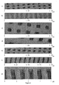
- the cured substrate resist was examined by AFM.
- Figure 3a displays an image of the substrate resist surface (surface 22 in figure 2f ) with dimensions of the applied Ni stamp pattern given in the caption of figure 3a .
- Table 1 water [°] 1,5-pentane diol [°] Diiodomethane [°] Ethylene Glycol [°] 1 Ni stamp patterned 107,6 87,5 92,5 - 2 Ni stamp non-patterned 106,3 81,4 87,7 - 3 IPS102 104,2 86,1 79,0 - 4 IPS105 105,1 86,5 86,2 - 5 IPS110 105,4 83,5 89,7 - 6 IPS50 100,7 - 78,8 88,1 7 IPS70/95 100,2 - - - 8 SR35 82,0 67,4 72,1 - 9 SR02 85,3 57,0 57,6 - 10 SR20/47 79,1 54,3 47,1 - Table 2: Column ⁇ Column 1: Template Column 2: Surface energy of the template Column 3: Replica Column 4: Surface energy of the replica Column 5: Interface parameters Group
Description
- The present invention relates to Nano-Imprinting in general and especially to the polymer mold with anti-sticking or anti-adhesion properties.
- One of the most powerful techniques for reproducing nanostructures - i.e. structures in the order of 100 nm or smaller- is nanoimprint lithography (NIL). In nanoimprint lithography an inverted copy of the surface pattern of a template - often called a stamp - is transferred into an object, comprising a substrate and, applied thereto, a film of a moldable layer often called resist, e.g. a polymer material. After heating the object to a temperature above the glass transition temperature of the polymer film, the stamp is pressed towards the film, cooled and released from the stamp - often called demolding - to give a polymer film with the desired pattern. This process is defined as a "thermal imprint process". Alternatively, a photo-resist material, i.e. a resin composition, which cures upon exposure to photon radiation, covers the substrate. This so-called "Photon-imprint process" requires that either the substrate or the stamp is transparent. In a process subsequent to the imprint, the object - comprising the substrate and the patterned polymer film - can be post-processed, e.g. by etching of the substrate within the imprinted regions to transfer the pattern to a target surface of the substrate.
- A method for transferring a pattern from a template to an object in an imprint process has been suggested, which involves a two-step process, which is described in JPA no.
2008-515059 US patent application no. 11/450377 US patent application no. 11/268574 US patent application no. 11/305157 - The template or master used in an imprint process is generally a high cost product, and wear or damages to the template should therefore be minimized. The template may be made of any material, but is often made of Si, Ni, Ti, other metals, or quartz, optionally provided with an anti-stick layer. On the other hand, the object to be imprinted is often made of a relatively hard material, such as glass, quartz, a metal, a metal-oxide, silicon, or another semiconductor material, sometimes coated with different layers comprising metal, alloys, organic or carbonaceous materials. On their surfaces a comparatively soft moldable imprint layer is exposed. The imprinting of the object is a crucial moment, where parallel arrangement is important, and a very small residual layer of the moldable layer, often in the order of less than 10 nm, under the imprinted protruding structures is desired. Any non-parallel arrangement or excessive pressure may therefore cause damage to the template. By the suggested two-step imprint method, the template will only be used against a polymer material, which is softer than the template material, thereby minimizing the risk of damage.
- If the template and the substrate are not made of the same material, which they generally are not, they will typically have different thermal expansion coefficients. This means that during heating and cooling of the template and the substrate, the extent of expansion and contraction will be different. Even though the dimensional change is small, it may be devastating in an imprint process, since the features of the pattern to be transferred are in the order of micrometers or even nanometers. The result may therefore be reduced replication fidelity.
- One of the most crucial properties in the photon-based 2-step imprint process is the anti-sticking or anti-adhesion properties between both interfaces of 1) the original template and the IPS resist and 2) the cured and patterned I PS resist and the substrate resist. Stamp materials with low surface energies are for example known from
US 2008/0000373 . Dae-Gem Choi et al., Langmuir, 2005, 21, 9390-9392, describes intermediate molds comprising a hybrid polymer material. - A method for transferring a pattern from a template to an object in an imprint process has been suggested, which involves a photon-based two-step process. In the first step, a template having a structured surface is contacted with a polymer material to produce a flexible polymer replica having an inverse structured surface pattern of the template surface, herein referred to as an intermediate polymer stamp (IPS). In the second step, the IPS replica is used as a template in order to produce a second replica. It is coated with a moldable surface to give a replica displaying a pattern identical with the original template.
- The IPS is produced when a polymer carrier object coated with photo-polymerizable compounds, is pressed towards a template, deformed and cured with the STU™ process. After demolding, the patterned IPS will be applied as a new template to replicate its pattern in a photon based imprint process. Among the most crucial properties 2-step imprint process are the anti-sticking or anti-adhesion properties of both the interfaces of the original template and the IPS resist as well as the cured and patterned IPS resist and the substrate resist.
- It is an object of the invention to provide a material that comprising photo-reactive compounds with one or several types of chemical functionalities i.e. acrylates, epoxides or vinyl ethers. Additionally, the material comprises photo-initiators or catalysts and semi-fluorinated molecules. When contacting this material with a surface of a template, exhibiting low surface energy, the semi-fluorinated molecules will diffuse to the surface near region of that surface of the chemical composition facing the template surface. The material is coated on a polymer carrier object and used in an improved imprint process, having high replication fidelity, and which is easy and suitable to employ industrially.
- Table 1 displays results from contact angles measurements for water, 1,5-pentanediol, diiodomethane and ethylene glycol provided on different surfaces.
- Table 2 displays surface energies, together with their dispersion and polar contributions calculated from the contact angle results of table 1 applying the model of Owens, Wendt, Rabel and Kaelble. Additionally, the table contains the calculated work of adhesions and interface energies for different interfaces, calculated from the assorted surface energies contributions displayed in table 2 with the help of
equations 2 and 4. -
-
Figure 1 illustrates- a) the different layers covering the polymer carrier object, and
- b) the different layers covering the substrate.
-
Figure 2 :-
Figure 2 schematically shows the 2-step imprint process.
-
-
Figure 3 :-
Figure 3 displays AFM images of the substrate resist surfaces after performed imprints applying the 2-step imprint process. The different IPS and substrate resist formulations are provided by this invention. Stamps with various pattern sizes and the different IPS and substrate resist formulations have been applied.
-
- The original stamp or template is usually equipped with an anti-sticking layer (i.e. a self assembling monolayer film) in order to decrease its surface energy, which is described in Japanese patent no.
3892460 2006 US patent application no. 11/597570 - Semi-fluorinated molecules or fluoro-surfactants have the characteristic of lowering the surface energy of a liquid phase efficiently even at low concentrations. Thus, the introduction of fluoro-surfactants into a composition comprising photo-reactive compounds can lower the surface energy by forming a concentrated fluorocarbon layer at the surface of the liquid. A phase segregation occurs into a fluoro-surfactants-rich and a fluoro-surfactants-poor phase which can thermodynamically be described by Gibbs adsorption equation

- with Γ the surface (interface) excess concentration, c the molecular concentration of the fluoro-surfactant, γ the surface (interface) energy and R/ T the molecular gas constant/ temperature (see e.g. [Hiemenz, Rajagopalan]). If fluoro-surfactants are introduced into a composition comprising photo-reactive compounds, dγ /dC will become negative and therefore Γ positive. This leads to an enrichment of the fluoro-surfactants at the surface (interface) in order to decrease the surface (interface) energy.
- Regarding the 2-step imprint process, in the first step the stamp equipped with an anti-sticking layer will be pressed against a non-cured resist composition comprising fluoro-surfactants. The non-cured resist can be regarded as a liquid with high viscosity. The resist is deposited onto a polymer carrier object.
- Herein, the term "polymer carrier object" refers to a flexible, ductile, and transparent polymer specimen, comprising a thermoplast or a thermosetting polymer material. Typical materials are polycarbonate, polymethyl methacrylate (PMMA), polyethylene terephthalate (PET), and polyethylene naphthalate (PEN). Preferably, the polymer carrier object is homogenously made of one or more of these materials, but in an alternative embodiment the material may comprise other compounds as well. The polymer carrier object might be a thin polymer film fabricated in an extrusion process (typical thickness 50-200 micrometer) [Osswald] or a disk, fabricated with the help of an injection molding process (typical thickness 300 micrometer up to 1 millimeter).
- The low surface energy of the anti-sticking treated stamp (<20 mJ/m2 - see table 2) leads to an enrichment of the fluoro-sufactants at the resist/ stamp interface in order to minimize its interface energy (see Equation 1). The occurred phase segregation will affect the work of adhesion at the resist/ stamp interface, defined as:

- The work of adhesion can be regarded as the required work necessary to remove a liquid (e.g. resist) from a solid surface (e.g. stamp) (see e.g. [Adamson, Gast]). Usually, the work of adhesion WA of an interface (Eq. 2) comprising a stamp equipped with an anti-sticking layer and a resin composition comprising fluoro-surfactants is lower than that comprising an anti-sticking treated stamp and a resist without fluoro-surfactants, because in the first case both the stamp and the non-cured resist exhibit low surface energies, γstamp and γresist, and WA will be low even if the interface energy γstamp, resist is very small. On the other hand the fluoro-surfactant containing resist will obtain a more pronounced wettability with the stamp (i.e. smaller contact angles will be observed) - compared to the non-fluorine-containing species because the fluoro-surfactants are reducing the surface energy of the resist- and additionally also the interface energy of the stamp resist interface - acting as a wetting agent. The better wetting leads to a more pronounced and faster penetration of the pattern of the stamp under the assumption that the viscosity of resist remains almost unchanged by the introduction of low concentrations of the fluoro-surfactants. This behavior can be expressed by the following relation:

where z(t) is the vertical penetration distance of the resist into a pattern comprising cylindrical pores with a diameter r at a time t. The liquid has the viscosity η and the surface energy γresist, θ∞ is the contact angle after infinite times and a and c adjustable parameters (see e.g. [Pocius]). Equation is valid if no external pressure will be applied. - Thus the introduction of fluoro-surfactants has three advantages; first the increased pattern penetration enables both the reduction of the applied pressure between the stamp and the IPS in the imprint process, second is the decrease of the process time and third, the reduced surface energy that improves the wettability and - after curing - adhesion with impurity particles, resulting in a better cleaning effect of the stamp.
- Table 1 shows typical contact angles with water, 1,5-pentanediol, diiodomethane and ethylene glycol. Water contact angles higher than 100° could be observed for the different formulations after curing. Additionally, when the surface energy is divided into polar forces and dispersion forces, according to the model of Owens and Wendt, the surface energy γ of the IPS is strongly dominated by the dispersion contribution γd whereas the polar contribution γp is very low due to the non-polarity of the fluoro-surfactants.
- Table 2 presents some parameters which are important for the characterization of different surfaces or interfaces of the stamp/ IPS, e.g. γ, γd, γp, WA, γ 1,2. The different parameters have been calculated from contact angles measurements (table 1). As expected, the interfaces are characterized by low work of adhesions, WA, of approx. 30 mJ/m2 and low interface energies, γ1,2 of almost 0 mJ/m2 up to below 1 mJ/ m2. A low work of adhesion is very adventurous when a joint should exhibit low adhesion strength so that demolding can be performed easily. Low interface energies are found when the two surfaces establishing an interface are chemically very similar e.g. in their polarity. For example a joint consisting of two completely similar materials exhibits an interface energy of 0 mJ/m2.
- The large interfacial energies will occur if the applied materials located at the interface of a joint are unlike, e.g. one exhibits high polarity and one is almost nonpolar. In the model of Owens and Wendt the work of adhesion can be expressed as:

- On the other hand a higher polar contribution γ2 p will not increase WA drastically, because of the low value of γ1 p. However, a more polar substrate resist will downgrade the wetting properties. Wettability is a crucial property of adhesion. A non-cured resist that is composed of polar ingredients exhibits a high surface energy and therefore a high work of cohesion (Wc = 2γliquid). This high work of cohesion leads to reduced wetting behavior of the liquid with an IPS surface exhibiting low surface energy. According Equation [3] penetration with the nano-structured IPS surface is downgraded and - even more important - the diffusion into small sub-10 nm-sized pores or cavities located on the IPS surface is reduced.
- After curing of the substrate resist the work of adhesion WA of equations [2] and [4] has to be modified in a way to achieve the work, which is required to break an interfacial bond between two solid materials WB:

- Another crucial parameter is diffusion between the non-cured substrate resists and the cured IPS resist if the cured resist is soluble in the components of the non-cured one. For pronounced anti-adhesion properties the cured resist should be insoluble in the non-cured resist. At least, electrostatic interactions between the IPS and the substrate resist could be minimized when the two surfaces do not exhibit opposite electronegativity characters, which would reduce γP of Equation [4] concerning the acid-base model of Fowkes [Pocius].
- Formulations containing mixtures of different mono- or multi-functionalized monomers and/ or oligomers, which after curing exhibits high degrees of crosslinking and low solubility, are applied as imprint materials. The acrylate based resists are characterized by high reactivity and polymerize rapidly in the presence of photogenerated free radicals and in the absence of oxygen at ambient temperature. The acrylate-based resists are for many reasons attractive material, but generally suffer from drawbacks such as high oxygen sensitivity and large shrinkage upon polymerization. Cationic induced polymerization of epoxides and vinyl ethers is comparatively slow, but offers several advantages such as good mechanical properties of the resist, low shrinkage, and an oxygen insensitive process. The present innovation describes how material properties from different polymers may be combined by blending proper ratios of interpenetrating polymer networks (IPNs) forming a hybrid polymer system comprising for example both acrylates and epoxides [Vabrik et al]. The synthesis of IPNs is achieved by photoinitiated polymerization of monomers, which polymerize through different mechanisms, typically photoinitiated free radial mechanism and photoinitiated cationic mechanism. The developed IPS resist is a hybrid resist comprising both: acrylates and epoxides, or acrylates and vinyl ethers. Acrylate comprising hybrid resists are generally characterized by a fast curing of the acrylate monomers leading to a close to full conversion of the acrylates and lower conversions of the epoxides/vinyl ether. The high conversion of the acrylates circumvents polymerization of the remaining acrylates present close to the surface of the IPS resist and an acrylate-based substrate resist, which facilitates efficient demolding.
- Proper selection of both the photoinitiators and radiation wavelengths enables a sequential build-up of a hybrid IPNs [Decker], [Decker, Decker]. This refinement of the hybrid polymerization allows the synthesis of a highly cross-linked acrylate network, prior to the initiation of the epoxy network synthesis. This is achieved by exposing the non-cured IPS formulation to filtered radiation (wavelength >350 nm), absorbed solely by the free radical photoinitiator e.g. 2,4,6-trimethylbenzoylphenylphosphinate, but not by the cationic photoinitiator. In the second step the sample is exposed to unfiltered PHOTON BASED radiation, which is absorbed by the cationic photoinitiator e.g. triarylsulfonium hexafluorophosphate, thus initiating polymerization of the epoxy monomers within the existing acrylate polymer network forming the IPNs. The sequential polymerization is here presented as a promising technique for the improvement of material properties such as reduced polymer shrinkage, due to the low shrinkage of the epoxides, and higher imprint fidelity etc.
- The anti-sticking treatment of the IPS resist results in a low surface energy, necessary for enhanced release properties between in particular the IPS resist and the substrate resist. A low IPS surface energy leads to a low work of adhesion WA and - if the substrate resist is selected carefully - a high interfacial energy γ1,2. One class of molecules that have showed strong potential as efficient fluoro-surfactants, with the ability to diffuse to the surface of the mold resist forming an anti-sticking layer, are perfluoropolyether (PFPE) based derivatives end terminated with one or several chemical functionalities, such as (meth)acrylates. For example, the PFPE backbone has been linked to the (meth)acrylates via linear or branched aliphatic urethane block copolymers chain and is manufactured, which has the following structure:
Yp-X-CF2CF2O(CF2F2O)m(CF2O)nCF2CF2-X-Yp,
where X is an aliphatic urethane building block, Y is a (meth)acrylate and p equals one or two. The molecular weight of the PFPE part of the co-polymer is 1500-2000 g/mol and the ratio m/n is 1.5 to 2.5. - The substrate resist may be a purely acrylate based resist, or a hybrid resist, with material properties combined from the two types of polymers, comprising acrylates and vinyl ethers, or acrylates and epoxides.
- Composition 1 (referred to as "IPS50") is a purely acrylate-based IPS formulation containing approximately 0.25% by weight of the fluoro-surfactant Y-X-CF2CF2O(CF2F2O)m(CF2O)nCF2CF2-X-Y, where X is a short linear urethane block copolymers chain and Y is a methacrylate group.
- Composition 2 (referred to as "IPS70/95") is an acrylate/epoxide-hybrid IPS formulation containing approximately 1% by weight of a fluoro-surfactant with the structure:

- Composition 3 (referred to as "IPS105") is an acrylate/epoxide-hybrid IPS formulation containing approximately 1% by weight of the fluoro-surfactant Y2-X-CF2CF2O(CF2F2O)m(CF2O)nCF2CF2-X-Y2, where X is a long branched urethane block copolymers chain and Y is an acrylate group.
- Composition 4 (referred to as "IPS110") is an acrylate/epoxide-hybrid IPS formulation containing approximately 0.8% by weight of the fluoro-surfactant Y2-X-CF2CF2O(CF2F2O)m(CF2O)nCF2CF2-X-Y2, where X is a long branched urethane block copolymers chain and Y is an acrylate group, and 0.6% by weight of a fluoro-surfactant with the structure specified in
IPS composition 2. - Composition 5 (referred to as "IPS102") is a purely acrylate-based IPS formulation containing approximately 1% by weight of the fluoro-surfactant Y2-X-CF2CF2O(CF2F2O)m(CF2O)nCF2CF2-X-Y2, where X is a long branched urethane block copolymers chain and Y is an acrylate group.
- Substrate resist 1 (referred to as "SR20/47") is a purely acrylate-based substrate resist formulation without functionalized siloxanes.
- Substrate resist 2 compositions (referred to as "SR02") are a purely acrylate-based substrate resists formulations containing functionalized siloxanes.
- Substrate resist 3 compositions (referred to as "SR35") are a purely acrylate-based substrate resists formulations without functionalized siloxanes.
- The two
material assemblies figures 1 a and 1b, respectively, can be regarded as the essential prerequisite to succeed the two-step process illustrated infigure 2 . Here, the first step is illustrated infigs. 2a-2c and the second step infigs. 2d-2f . Infig. 2a the stamp ortemplate 10, composed of e.g. silicon, quartz, nickel or other metal such as aluminum or titanium, an alloy or even a polymer material has a patterned surface 9, comprising ribs, grooves, protrusions or recesses, having heights and widths in the order of micrometers or nanometers. The template surface 9 is equipped with an anti-adhesion layer 8. Thetemplate 10 is placed with the surface of the anti-adhesion layer 8 in a way facing and contacting asurface 6 of thespecimen 1. After placing, a pressure between 1-40 bars is applied on the backsides of either thetemplate 10 or thepolymer carrier object 2 in order to press thetemplate 10 and thespecimen 1 together. The resist 5 will fill the cavities of the template surface 9, equipped with an anti-sticking layer 8. Additionally, the fluoro-surfactants will predominately settle at the surface 6 - now facing the template anti-sticking layer 8 - or within the surface-near region of the resist 5 in order to minimize the interface energy of the interface between the template anti-sticking layer 8 and the resistsurface 6. - The sandwich arrangement - consisting of a
template 10 equipped with an anti-sticking layer 8, apolymer carrier object 2, and photo-polymerizable resist 5 and maybe an adhesion promoter 4 - is irradiated with ultraviolet light either through the backside of thetemplate 10 or through thepolymer carrier object 2 as displayed infig 2b ). In the first case the template has to be transparent, whereas in the second case the polymer carrier object has to fulfill this requirement. - A photon radiation cures the resist and creates a solidified, low-surface-energy replica, having a pattern that is inversed to that of the original template. Once the photo curing is completed, the
template 10 is separated or demolded from theflexible polymer replica 11 leaving a relief image on thesurface 13 of the solidifiedphotopolymer film 12, coated on thepolymer carrier object 2 as displayed inFig 2c . - After demolding neither plastic deformations of patterns of the
surface 13 can be observed nor resist rip-off, - e.g. residuals of the cured resist 12 or the non-cured resist 5 that has been ruptured from thepolymer carrier object 2 upon the performed imprint will cover the surface of thetemplate 10. This is due to pronounced anti-sticking or anti-adhesion properties of the interface between the resistsurface 13 and the template anti-sticking film 8 due to a well-defined material composition of the applied materials and their surfaces as described in the chapters "Anti-Adhesion Properties of the IPS comprising a fluoro-surfactant-containing resist composition". Theflexible polymer replica 11 herein is referred to as an intermediate polymer stamp (IPS). - In the second step of the two-step process the
IPS 11 is used to transfer the pattern of itssurface 13 to a target substrate as illustrated inFigs 2d) - 2f ). Here, thesurface 13 of theflexible polymer stamp 11 will be placed in contact with asurface 19 of anobject 14 comprising asubstrate 15 having asurface 16 covered by a thinmoldable surface layer 18 of a non-cured photo curable resist. A thinorganic layer 17 acting as an adhesion promoter might be placed in-between thesubstrate surface 16 and the resist 18. - As illustrated in
fig. 2e with the help of an applied pressure lying between 1 to 40 bars theIPS 11 andobject 14 will be forced together and after applied exposure of the photo-curable resist 18 to radiation, the resist will be cured. After release an inversion of the pattern located on thesurface 13 of theIPS 11 has been formed in the surface 22 of thelayer 21, as shown infig. 2f . Usually, theIPS 11 has to be transparent to the applied radiation or shows minor absorbance in order to transmit a sufficient amount of radiation necessary for curing the resist 18 upon exposure to radiation. - Several IPS and substrate resist formulations has been evaluated which fulfill the requirement of this invention to provide materials for an improved imprint process, having high replication fidelity, and which is easy and suitable to employ industrially. The different formulations could easily be applied within the 2-step process - schematically described in
figure 2 - without any further anti-sticking treatment of the IPS (surface 13 infigure 2c or 2d ), and thus avoids the need of an external process, as for example a plasma treatment, and/ or a coating of an additional thin film. Five Selected examples of Ni stamps or templates having patterns as small as sub 100 nm range they were covered by a thin anti-sticking film - as described in Japanese patent no.3892460 2006 - Table 1 displays results for water, 1,5-pentanediol, diiodomethane and ethylene glycol applied to different surfaces. The contact angle measurements have been carried out with a Tracker contact-angle measurement instrument from Teclis. The investigated surfaces can be divided into three different categories:
- 1)
Row 1 androw 2 display data for the original Ni template or stamp (surface 8 offigure 2a ). Due to the anti-sticking treatment of the Ni templates the hydrophobic surfaces are characterized by high contact angles observed for water (107,6° and 106,3°, respectively). - 2)
Row 3 to row 7 display contact angles of the different IPS resists containing semi-fluorinated molecules acting as fluoro-surfactants (surface 6 offigure 1a and2a ). The investigated IPS resist solutions are IPS102, IPS105, IPS110, IPS50 and IPS70/95 and the different formulations have been prepared by spin-coating onto silicon wafers, pretreated with adhesion promoters, such as methacrylate silanes. The resulting film thicknesses were measured to be 600-1200 nm. After curing the fluoro-surfactants are cross-linked which generates a fluorinated surface, with pronounced hydrophobicity. - Row 8 to row 10 display data for the substrate resist (surface 19 of
figure 1b and2d ). The investigated substrate resist solutions are SR35, SR02, and SR20/47, and the different formulations have been prepared by spin-coating onto silicon wafers, pretreated with adhesion promoters, such as methacrylate silanes. The resulting film thicknesses are approximately 70 nm for SR02; and 600 nm for SR35 and SR20/47. The contact angles observed for the surfaces of the cured non-fluorinated substrate resists (rows 8-10) are significantly lower than those observed for the surfaces of the fluorinated IPS resists (rows 3-7). - With the help of the contact angles displayed in Table 1 the surface energies, together with their dispersion and polar contributions have been calculated utilizing the model of Owens, Wendt, Rabel and Kaelble. The different values are displayed in table 2
columns 2 and 4. Additionally, the calculated work of adhesions and interface energies for different interfaces, calculated from the assorted surface energies contributions with the help ofequations 2 and 4, are displayed in table 2, column 5. The calculated parameters should represent the following interfaces, divided in five groups: -
Group 1 displays parameters characterizing the surfaces of the original Ni template, several cured-IPS resist compositions, and their interfaces (surfaces 8 offigure 2a and thesurfaces 6 offigures 1a and2a after curing). The patterned Ni stamp surface is characterized by low surface energy dominated by the dispersion contribution γd. - The parameters displayed in
groups 2 to 5 stand for the interfaces of several IPS resist compositions and several substrate resist compositions. Each group represents the interfaces of one IPS resist to one or two substrate resists. The values represents the surfaces and interfaces between thesurface 13 offigures 2c and 2d and thesurface 19 offigures 1b and2d after curing. The calculated surface energies of the substrate resists are significantly larger than those of the surfactant containing IPS resists. - A 1,5 µm thick film of the IPS resists IPS70/95 was spin-coated onto a polycarbonate film having a thickness of 125 µm. A 2-step imprint process was carried out according to
figure 2 . The anti-sticking treatedNi stamp 1 was pressed against the polymer film for 60 sec with a pressure of 30 bars, the resist was cured with photon radiation for 90 sec as illustrated infigure 2b . During the exposure time the applied pressure was kept at 30 bars. Afterwards, the Ni stamp was separated from the cured IPS. The IPS comprising a polycarbonate film equipped with a completely cured IPS resist was applied in the second imprint process (figure 2d ). A SR02 substrate resist was spin-coated to a thickness of 50 nm onto a silicon wafer, pretreated with an acrylate silane employed as an adhesion promoter for improved adhesion. The second imprint was performed as described above with a photon radiation time of 30 sec (figure 2e ). After demolding, the cured substrate resist was examined by AFM.Figure 3a displays an image of the substrate resist surface (surface 22 infigure 2f ) with dimensions of the applied Ni stamp pattern given in the caption offigure 3a . - An imprint with
Ni Stamp 2 was performed according to the description of Example 1 using a 1 µm thick SR20/47 film as substrate resist in the second imprint step and - in the second imprint step - with a photon radiation time of 60 sec.Figure 3b displays an image of the substrate resist surface with dimensions of the applied Ni stamp pattern given in the caption offigure 3b . - An imprint with
Ni Stamp 3 was performed according to the description of Example 1. However, the applied substrate resist (SR02) was 70 nm thick.Figure 3c displays an image of the substrate resist surface with dimensions of the applied Ni stamp pattern given in the caption offigure 3c . - An imprint with
Ni Stamp 3 was performed according to the description of Example 3 using a 1 µm thick IPS110 film as an IPS resist in the first imprint step.Figure 3d displays an image of the substrate resist surface with dimensions of the applied Ni stamp pattern given in the caption offigure 3d . - An imprint with
Ni Stamp 1 was performed according to the description of Example 1 using a 1.5 µm thick IPS105 film as an IPS resist in the first imprint step.Figure 3e displays an image of the substrate resist surface with dimensions of the applied Ni stamp pattern given in the caption offigure 3e . - An imprint with Ni Stamp 4 exhibiting a smaller structure sizes, was performed according to the description of Example 5.
Figure 3f displays an image of the substrate resist surface with dimensions of the applied Ni stamp pattern given in the caption offigure 3f . - An imprint with Ni Stamp 5, exhibiting a larger pattern, was performed according to the description of Example 1 using a 1.5 µm thick IPS50 film as IPS in the first imprint step and a 1 µm thick SR20/47 film as substrate resist in the second imprint step and an with a photon radiation time of 60 sec in both imprint steps.
Figure 3g displays an image of the substrate resist surface with dimensions of the applied Ni stamp pattern given in the caption offigure 3g .Table 1: water [°] 1,5-pentane diol [°] Diiodomethane [°] Ethylene Glycol [°] 1 Ni stamp patterned 107,6 87,5 92,5 - 2 Ni stamp non-patterned 106,3 81,4 87,7 - 3 IPS102 104,2 86,1 79,0 - 4 IPS105 105,1 86,5 86,2 - 5 IPS110 105,4 83,5 89,7 - 6 IPS50 100,7 - 78,8 88,1 7 IPS70/95 100,2 - - - 8 SR35 82,0 67,4 72,1 - 9 SR02 85,3 57,0 57,6 - 10 SR20/47 79,1 54,3 47,1 - Table 2: Column → Column 1: Template Column 2: Surface energy of the template Column 3: Replica Column 4: Surface energy of the replica Column 5: Interface parameters Group ↓ γ [mJ/m2] γd [mJ/m2] γp [mJ/m2] γ [mJ/m2] γd [mJ/m2] γp [mJ/m2] WA [mJ/m2] γ1,2 [mJ/m2] Group 1 Ni stamp patterned 13,14 11,37 1,77 IPS102 19,18 18,03 1,15 31,50 0,83 IPS105 16,09 14,44 1,65 29,04 0,19 IPS110 14,77 12,82 1,95 27,86 0,05 Group 2 IPS102 19,18 18,03 1,15 SR35 29,30 21,69 7,61 45,47 3,01 SR02 33,69 29,95 3,74 50,63 2,25 Group 3 IPS105 16,09 14,44 1,65 SR35 29,30 21,69 7,61 42,48 2,91 SR02 33,69 29,95 3,74 46,56 3,22 Group 4 IPS110 14,77 12,82 1,95 SR35 29,30 21,69 7,61 41,10 3,01 SR02 33,69 29,95 3,74 44,95 3,87 Group 5 IPS15 20,15 18,13 2,02 SR20/47 36,25 31,64 4,61 54,00 2,40 -
- [Hiemenz, Rajagopalan] P.C. Hiemenz and R. Rajagopalan, "Principles of Colloid and Surface Chemistry", Marcel Dekker, Inc., New York, Third Edition, 1997 . [Adamson, Gast] A. W. Adamson and A.P. Gast "Physical Chemistry of Surfaces", John Wiley & Sons, Inc., New York, Sixth Edition, 1997 .
- [Pocius] A. V. Pocius "Adhesion and Adhesive Technology", Hanser Publishers, Munich, Second Edition, 2002 .
- [Oswald] T. Osswald, J. P. Hernandez-Ortiz, "Polymer Processing - Modelling and Simulation" Hanser Publishers, Munich 2006 .
- [Vabrik el al] R. Vabrik, I. Czajlik, G. Tury, I. Rusznak, A. Ille, A. Vig, "A study of epoxy resin - acrylated polyurethane semi-interpenetrating polymer networks", Journal of applied polymer science, Vol 68, 1998, pp 111-119 .
- [Decker] C. Decker, "PHOTON BASED-radiation curing chemistry", Pigment & Resin Technology, Vol 30(5), 2001, pp 278-286 .
- [Decker, Decker] C. Decker, D. Decker, "Photoinitiated polymerization of vinyl ether and acrylate monomer mixtures", J.M.S.-Pure Appl. Chem., Vol A34(4), 1997, pp 605-625 .
Claims (11)
- A pre-curing polymer mold made in an intermediate imprint stamp process, wherein the polymer mold comprises a polymer carrier object covered by a chemical composition comprising photo-polymerizable monomers and/or oligomers, photo-initiators with the ability to initiate polymerization, and semi-fluorinated molecules, which are soluble in said chemical composition and are completely or partly terminated by chemical functionalities with the ability to bind covalently to said chemical composition, wherein the semi-fluorinated molecules are predominantly located on a patterned surface of the polymer mold, wherein said chemical composition is a hybrid comprising polymerizable mono- or multifunctional acrylate monomers, polymerizable mono- or multifunctional epoxides or vinyl ethers and at least one free radical photoinitiator as well as at least one cationic photoinitiator.
- The polymer mold of claim 1, wherein said semi-fluorinated molecules have the ability to diffuse to the surface near region of that surface of the chemical composition facing the template surface.
- The polymer mold of claim 1, wherein said semi-fluorinated molecules are PFPE co-polymers with the structure Yp-X-CF2CF2O(CF2F2O)m(CF2O)nCF2CF2-X-Yp, where X is an aliphatic urethane block, Y is an acrylate or a methacrylate, m and n are integers, and p equals 1 - 3, with a molecular weight of the PFPE part of the copolymer of 800-2000 g/mol.
- The polymer mold of any of claims 1 - 3, wherein said chemical composition contains polymerizable mono- or multifunctional acrylate-based monomers and at least one free radical photoinitiator.
- The polymer mold of claim 3, wherein said X in the chemical formula of claim 3 is an aliphatic urethane block and the chemical composition is a hybrid comprising interpenetrating networks.
- The polymer mold of any of claims 1 -2, wherein said semi-fluorinated molecules have chemical functionalities making them suitable to bind covalently to acrylate, epoxide or vinyl ether network upon curing.
- The polymer mold of any of claims 1 - 6, wherein said surface of the polymer mold exhibits a surface energy of 35 mJ/m2 or smaller (preferably smaller than 20 mJ/m2).
- The polymer mold of any of claims 1 - 7, wherein said polymer mold after curing is applicable as a template in an imprint process.
- The polymer mold of claims 1 - 7, wherein said polymer mold comprises semi-fluorinated moieties, which are predominantly located on the surface and on the surface near region of the patterned surface is contacted with a surface of a chemical composition, comprising photo-polymerizable compounds, photo-initiators or catalysts, with the ability to initiate polymerization, and after curing of said chemical composition to be performed in order to produce a replica, the interface between the polymer mold and the replica exhibits low work of adhesion and a not negligible interface energy.
- The polymer mold of claim 9, wherein said work of adhesion of the polymer mold/ replica interface is smaller than 65 mJ/m2 (preferably smaller than 30 mJ/m2) and the interface energy of the polymer mold/ replica interface is larger than 1 mJ/m2 (preferably larger than 4 mJ/m2).
- A method of forming a mold in an intermediate imprint stamp process, wherein the mold comprises a polymer carrier object covered by a chemical composition, wherein said chemical composition is a hybrid comprising polymerizable mono- or multifunctional acrylate monomers, polymerizable mono- or multifunctional epoxides or vinyl ethers and at least one free radical photoinitiator as well as at least one cationic photoinitiator, wherein the mold is contacted and pressed to a surface of a patterned template exhibiting low surface energy, in order to deform the surface of the chemical composition followed by curing with the help of photon radiation and demolding.
Priority Applications (7)
| Application Number | Priority Date | Filing Date | Title |
|---|---|---|---|
| EP08172338.9A EP2199854B1 (en) | 2008-12-19 | 2008-12-19 | Hybrid polymer mold for nano-imprinting and method for making the same |
| SG200908080-5A SG162673A1 (en) | 2008-12-19 | 2009-12-04 | Process and method for modifying polymer film surface interaction |
| US12/635,296 US8426025B2 (en) | 2008-12-19 | 2009-12-10 | Process and method for modifying polymer film surface interaction |
| JP2009283149A JP5663162B2 (en) | 2008-12-19 | 2009-12-14 | Process and method for altering polymer film surface interactions |
| TW98143046A TWI443138B (en) | 2008-12-19 | 2009-12-16 | Process and method for modifying polymer film surface interaction |
| CN200910261312.7A CN101799626B (en) | 2008-12-19 | 2009-12-17 | For the technological process control of modifying polymer film surface interaction |
| KR1020090126771A KR101621381B1 (en) | 2008-12-19 | 2009-12-18 | Process and method for modifying polymer film surface interaction |
Applications Claiming Priority (1)
| Application Number | Priority Date | Filing Date | Title |
|---|---|---|---|
| EP08172338.9A EP2199854B1 (en) | 2008-12-19 | 2008-12-19 | Hybrid polymer mold for nano-imprinting and method for making the same |
Publications (2)
| Publication Number | Publication Date |
|---|---|
| EP2199854A1 EP2199854A1 (en) | 2010-06-23 |
| EP2199854B1 true EP2199854B1 (en) | 2015-12-16 |
Family
ID=40481697
Family Applications (1)
| Application Number | Title | Priority Date | Filing Date |
|---|---|---|---|
| EP08172338.9A Active EP2199854B1 (en) | 2008-12-19 | 2008-12-19 | Hybrid polymer mold for nano-imprinting and method for making the same |
Country Status (7)
| Country | Link |
|---|---|
| US (1) | US8426025B2 (en) |
| EP (1) | EP2199854B1 (en) |
| JP (1) | JP5663162B2 (en) |
| KR (1) | KR101621381B1 (en) |
| CN (1) | CN101799626B (en) |
| SG (1) | SG162673A1 (en) |
| TW (1) | TWI443138B (en) |
Cited By (1)
| Publication number | Priority date | Publication date | Assignee | Title |
|---|---|---|---|---|
| KR20190009502A (en) * | 2017-07-19 | 2019-01-29 | 서강대학교산학협력단 | Injection mold for manufacturing probe of atomic force microscopy and manufacturing method thereof |
Families Citing this family (48)
| Publication number | Priority date | Publication date | Assignee | Title |
|---|---|---|---|---|
| WO2009113519A1 (en) * | 2008-03-12 | 2009-09-17 | 富士フイルム株式会社 | Method of fabricating a template for a concave array mold, a concave array mold and a needle array sheet |
| US8877298B2 (en) * | 2008-05-27 | 2014-11-04 | The Hong Kong University Of Science And Technology | Printing using a structure coated with ultraviolet radiation responsive material |
| EP2199855B1 (en) * | 2008-12-19 | 2016-07-20 | Obducat | Methods and processes for modifying polymer material surface interactions |
| EP2617548B1 (en) * | 2010-09-16 | 2016-08-31 | NGK Insulators, Ltd. | Use of a forming mold for yielding a molded product made from a slurry |
| JP5658001B2 (en) * | 2010-11-11 | 2015-01-21 | 旭化成イーマテリアルズ株式会社 | Resin mold |
| JP5306404B2 (en) * | 2011-03-25 | 2013-10-02 | 株式会社東芝 | Pattern formation method |
| US10497601B2 (en) * | 2011-09-20 | 2019-12-03 | Ev Group E. Thallner Gmbh | Device and method for coating of a carrier wafer |
| US9278857B2 (en) * | 2012-01-31 | 2016-03-08 | Seagate Technology Inc. | Method of surface tension control to reduce trapped gas bubbles |
| EP2821096B1 (en) * | 2012-02-29 | 2019-05-22 | Toppan Printing Co., Ltd. | Method for manufacturing needle-like material |
| CN104302569B (en) * | 2012-05-16 | 2017-10-13 | 奥的斯电梯公司 | Pulley for elevator device |
| CA2877744C (en) * | 2012-06-28 | 2021-04-13 | Henkel Ag & Co Kgaa | A method of manufacturing a composite insert |
| CN106459326B (en) | 2013-12-06 | 2019-08-13 | 株式会社Lg化学 | Block copolymer |
| CN105899559B (en) | 2013-12-06 | 2018-05-25 | 株式会社Lg化学 | Block copolymer |
| CN105873968B (en) | 2013-12-06 | 2018-09-28 | 株式会社Lg化学 | Block copolymer |
| US10227438B2 (en) | 2013-12-06 | 2019-03-12 | Lg Chem, Ltd. | Block copolymer |
| WO2015084132A1 (en) | 2013-12-06 | 2015-06-11 | 주식회사 엘지화학 | Block copolymer |
| EP3078685B1 (en) | 2013-12-06 | 2020-09-09 | LG Chem, Ltd. | Block copolymer |
| JP6432847B2 (en) | 2013-12-06 | 2018-12-05 | エルジー・ケム・リミテッド | Block copolymer |
| EP3078689B1 (en) | 2013-12-06 | 2020-12-02 | LG Chem, Ltd. | Block copolymer |
| JP6432846B2 (en) | 2013-12-06 | 2018-12-05 | エルジー・ケム・リミテッド | Block copolymer |
| WO2015084127A1 (en) | 2013-12-06 | 2015-06-11 | 주식회사 엘지화학 | Block copolymer |
| EP3078687B1 (en) | 2013-12-06 | 2020-06-03 | LG Chem, Ltd. | Block copolymer |
| JP6410327B2 (en) | 2013-12-06 | 2018-10-24 | エルジー・ケム・リミテッド | Block copolymer |
| CN105980342B (en) | 2013-12-06 | 2019-02-15 | 株式会社Lg化学 | Monomer and block copolymer |
| EP3078693B1 (en) | 2013-12-06 | 2021-01-27 | LG Chem, Ltd. | Block copolymer |
| EP3225641B1 (en) | 2014-09-30 | 2021-11-24 | LG Chem, Ltd. | Block copolymer |
| JP6538159B2 (en) | 2014-09-30 | 2019-07-03 | エルジー・ケム・リミテッド | Block copolymer |
| US10281820B2 (en) | 2014-09-30 | 2019-05-07 | Lg Chem, Ltd. | Block copolymer |
| US10295908B2 (en) | 2014-09-30 | 2019-05-21 | Lg Chem, Ltd. | Block copolymer |
| EP3203497B1 (en) | 2014-09-30 | 2023-11-29 | LG Chem, Ltd. | Method for producing patterned substrate |
| JP6451966B2 (en) | 2014-09-30 | 2019-01-16 | エルジー・ケム・リミテッド | Block copolymer |
| CN107075028B (en) | 2014-09-30 | 2020-04-03 | 株式会社Lg化学 | Block copolymer |
| US10310378B2 (en) | 2014-09-30 | 2019-06-04 | Lg Chem, Ltd. | Block copolymer |
| US10633533B2 (en) | 2014-09-30 | 2020-04-28 | Lg Chem, Ltd. | Block copolymer |
| US10287430B2 (en) | 2014-09-30 | 2019-05-14 | Lg Chem, Ltd. | Method of manufacturing patterned substrate |
| JP6531898B2 (en) * | 2015-03-12 | 2019-06-19 | ニッタ株式会社 | Mold for imprint, method of manufacturing the same, and method of manufacturing microstructure |
| JP6141500B2 (en) * | 2015-09-08 | 2017-06-07 | キヤノン株式会社 | Substrate pretreatment to reduce filling time in nanoimprint lithography |
| US20170066208A1 (en) | 2015-09-08 | 2017-03-09 | Canon Kabushiki Kaisha | Substrate pretreatment for reducing fill time in nanoimprint lithography |
| US10488753B2 (en) | 2015-09-08 | 2019-11-26 | Canon Kabushiki Kaisha | Substrate pretreatment and etch uniformity in nanoimprint lithography |
| US10134588B2 (en) * | 2016-03-31 | 2018-11-20 | Canon Kabushiki Kaisha | Imprint resist and substrate pretreatment for reducing fill time in nanoimprint lithography |
| US10620539B2 (en) | 2016-03-31 | 2020-04-14 | Canon Kabushiki Kaisha | Curing substrate pretreatment compositions in nanoimprint lithography |
| US10095106B2 (en) | 2016-03-31 | 2018-10-09 | Canon Kabushiki Kaisha | Removing substrate pretreatment compositions in nanoimprint lithography |
| US10509313B2 (en) | 2016-06-28 | 2019-12-17 | Canon Kabushiki Kaisha | Imprint resist with fluorinated photoinitiator and substrate pretreatment for reducing fill time in nanoimprint lithography |
| US10317793B2 (en) | 2017-03-03 | 2019-06-11 | Canon Kabushiki Kaisha | Substrate pretreatment compositions for nanoimprint lithography |
| EP3511292A1 (en) * | 2018-01-10 | 2019-07-17 | SABIC Global Technologies B.V. | A hydrophobic impact textured surface and a method of making the same |
| KR102427286B1 (en) * | 2018-11-29 | 2022-07-29 | 도레이첨단소재 주식회사 | Double-sided adhesive film for bonding heterogeneous substrates, and laminated film and display device including the same |
| JP7358113B2 (en) * | 2019-08-19 | 2023-10-10 | キヤノン株式会社 | Mold, imprint device, and article manufacturing method |
| US20230257496A1 (en) * | 2022-02-11 | 2023-08-17 | Canon Kabushiki Kaisha | Photocurable composition including a non-reactive polymer |
Family Cites Families (62)
| Publication number | Priority date | Publication date | Assignee | Title |
|---|---|---|---|---|
| GB559072A (en) | 1940-08-03 | 1944-02-02 | Budd Edward G Mfg Co | A method of making stamping dies |
| US2305433A (en) * | 1940-09-11 | 1942-12-15 | Jesse B Hawley | Method and apparatus for molding articles of thermoplastic, thermosetting, or resinous materials |
| NL68070C (en) | 1947-01-17 | |||
| US2883372A (en) * | 1957-03-14 | 1959-04-21 | Du Pont | Copolymers of ethylene and dihydrodicyclopentadiene |
| US4211617A (en) * | 1975-02-24 | 1980-07-08 | Mca Disco-Vision, Inc. | Process for producing a stamper for videodisc purposes |
| DD251847A1 (en) | 1986-07-31 | 1987-11-25 | Zeiss Jena Veb Carl | METHOD AND ARRANGEMENT FOR IMAGE COMPARISON |
| JPH0830106B2 (en) | 1989-06-24 | 1996-03-27 | 日本ゼオン株式会社 | Molding material |
| US5334424A (en) * | 1991-06-17 | 1994-08-02 | Nippon Zeon Co., Ltd. | Thermoplastic norbornene resin formed articles and sustrates for liquid crystal display |
| US5312794A (en) * | 1992-12-29 | 1994-05-17 | Shell Oil Company | Catalyst system for olefin polymerization |
| AU6752496A (en) | 1995-07-28 | 1997-03-05 | Ely Michael Rabani | Pattern formation, replication, fabrication and devices thereby |
| US5772905A (en) * | 1995-11-15 | 1998-06-30 | Regents Of The University Of Minnesota | Nanoimprint lithography |
| US20040137734A1 (en) * | 1995-11-15 | 2004-07-15 | Princeton University | Compositions and processes for nanoimprinting |
| JPH09330864A (en) | 1996-06-10 | 1997-12-22 | Ge Yokogawa Medical Syst Ltd | Method and mask for manufacturing composite piezoelectric material |
| JPH10330577A (en) | 1997-03-31 | 1998-12-15 | Mitsui Chem Inc | Cycloolefin resin molding and method for stamping character thereon |
| US6334960B1 (en) * | 1999-03-11 | 2002-01-01 | Board Of Regents, The University Of Texas System | Step and flash imprint lithography |
| DE19920941A1 (en) * | 1999-05-07 | 2000-11-16 | Krauss Maffei Kunststofftech | Method for producing plastic parts with an embossed structure and device for carrying out the method |
| SE515607C2 (en) | 1999-12-10 | 2001-09-10 | Obducat Ab | Device and method for fabrication of structures |
| DE10009246A1 (en) * | 2000-02-28 | 2001-08-30 | Mitsubishi Polyester Film Gmbh | White, biaxially-oriented, UV-stabilized polyester film, used e.g. for packaging light- or air-sensitive food, has at least one layer containing a cyclo-olefin copolymer and a UV stabilizer |
| DE10011652A1 (en) | 2000-03-10 | 2001-09-13 | Mitsubishi Polyester Film Gmbh | Biaxially oriented polyester film with high whiteness, process for its production and its use |
| WO2001070489A1 (en) | 2000-03-16 | 2001-09-27 | Mitsubishi Polyester Film, Llc | White polyester film with cycloolefin copolymer |
| KR100694036B1 (en) | 2000-06-01 | 2007-03-12 | 삼성전자주식회사 | Disc with grooves and pits of different depths and method for manufacturing thereof |
| WO2002009894A2 (en) | 2000-08-01 | 2002-02-07 | The Deflex Llc | Gas-vapor cleaning method and system therefor |
| JP4192414B2 (en) | 2000-09-14 | 2008-12-10 | 凸版印刷株式会社 | Lens sheet manufacturing method |
| KR101031528B1 (en) * | 2000-10-12 | 2011-04-27 | 더 보드 오브 리전츠 오브 더 유니버시티 오브 텍사스 시스템 | Template for room temperature, low pressure micro- and nano- imprint lithography |
| US6705853B1 (en) * | 2000-10-20 | 2004-03-16 | Durakon Industries, Inc. | Six station rotary thermoforming machine |
| US6953332B1 (en) * | 2000-11-28 | 2005-10-11 | St. Jude Medical, Inc. | Mandrel for use in forming valved prostheses having polymer leaflets by dip coating |
| US6422528B1 (en) * | 2001-01-17 | 2002-07-23 | Sandia National Laboratories | Sacrificial plastic mold with electroplatable base |
| US6815739B2 (en) * | 2001-05-18 | 2004-11-09 | Corporation For National Research Initiatives | Radio frequency microelectromechanical systems (MEMS) devices on low-temperature co-fired ceramic (LTCC) substrates |
| US20030071016A1 (en) | 2001-10-11 | 2003-04-17 | Wu-Sheng Shih | Patterned structure reproduction using nonsticking mold |
| TWI258142B (en) | 2002-01-08 | 2006-07-11 | Tdk Corp | Manufacturing method of stamper for manufacturing data medium, the stamper, and the stamper spacer with template |
| JP3749520B2 (en) | 2002-01-08 | 2006-03-01 | Tdk株式会社 | Manufacturing method of stamper for manufacturing information medium, stamper, and stamper intermediate with master |
| KR100487025B1 (en) * | 2002-02-28 | 2005-05-11 | 주식회사 루밴틱스 | Photo-curable resin composition for optical waveguide and optical waveguide prepared therefrom |
| EP1353229A1 (en) * | 2002-04-09 | 2003-10-15 | ASML Netherlands B.V. | Lithographic apparatus, device manufacturing method and device manufactured thereby |
| DE10217151A1 (en) * | 2002-04-17 | 2003-10-30 | Clariant Gmbh | Nanoimprint resist |
| US20030230817A1 (en) * | 2002-06-13 | 2003-12-18 | Agere Systems, Inc. | Mold for UV curable adhesive and method of use therefor |
| EP1513688B1 (en) | 2002-06-20 | 2006-11-29 | Obducat AB | Mold tool method of manufacturing a mold tool and storage medium formed by use of the mold tool |
| US20050146083A1 (en) * | 2002-06-20 | 2005-07-07 | Lennart Olsson | Method and device for transferring a pattern |
| US20040032063A1 (en) * | 2002-08-16 | 2004-02-19 | Peter Walther | Process for shaping plate-shaped materials and an arrangement for carrying out the process |
| WO2004021083A1 (en) | 2002-08-27 | 2004-03-11 | Obducat Ab | Device for transferring a pattern to an object |
| US7750059B2 (en) * | 2002-12-04 | 2010-07-06 | Hewlett-Packard Development Company, L.P. | Polymer solution for nanoimprint lithography to reduce imprint temperature and pressure |
| DE10311855B4 (en) * | 2003-03-17 | 2005-04-28 | Infineon Technologies Ag | Arrangement for transferring information / structures to wafers using a stamp |
| JP4061220B2 (en) * | 2003-03-20 | 2008-03-12 | 株式会社日立製作所 | Nanoprint apparatus and fine structure transfer method |
| EP1620205A2 (en) | 2003-04-04 | 2006-02-01 | Tecan Trading AG | Elastomeric tools for fabricating of polymeric devices and uses thereof |
| US20050191419A1 (en) * | 2003-04-11 | 2005-09-01 | Helt James M. | Fabrication of nanostructures |
| KR100568581B1 (en) * | 2003-04-14 | 2006-04-07 | 주식회사 미뉴타텍 | Composition for mold used in forming micropattern, and mold prepared therefrom |
| TW568349U (en) * | 2003-05-02 | 2003-12-21 | Ind Tech Res Inst | Parallelism adjusting device for nano-transferring |
| US7307118B2 (en) * | 2004-11-24 | 2007-12-11 | Molecular Imprints, Inc. | Composition to reduce adhesion between a conformable region and a mold |
| US20050084804A1 (en) * | 2003-10-16 | 2005-04-21 | Molecular Imprints, Inc. | Low surface energy templates |
| US7150844B2 (en) * | 2003-10-16 | 2006-12-19 | Seagate Technology Llc | Dry passivation process for stamper/imprinter family making for patterned recording media |
| US6939664B2 (en) * | 2003-10-24 | 2005-09-06 | International Business Machines Corporation | Low-activation energy silicon-containing resist system |
| GB0325748D0 (en) | 2003-11-05 | 2003-12-10 | Koninkl Philips Electronics Nv | A method of forming a patterned layer on a substrate |
| DE60336322D1 (en) | 2003-11-21 | 2011-04-21 | Obducat Ab | Nanoimprint lithography in multilayer systems |
| EP1538482B1 (en) | 2003-12-05 | 2016-02-17 | Obducat AB | Device and method for large area lithography |
| KR102005840B1 (en) * | 2003-12-19 | 2019-07-31 | 더 유니버시티 오브 노쓰 캐롤라이나 엣 채플 힐 | Methods for fabricating isolated micro- and nano- structures using soft or imprint lithography |
| DE102004005247A1 (en) * | 2004-01-28 | 2005-09-01 | Infineon Technologies Ag | Imprint-lithographic process for manufacturing e.g. MOSFET, involves structuring polymerized gate dielectric layer by imprint stamp that is used to form hole on layer, and etching base of hole till preset thickness of layer is reached |
| EP1594001B1 (en) | 2004-05-07 | 2015-12-30 | Obducat AB | Device and method for imprint lithography |
| KR101257881B1 (en) | 2004-05-28 | 2013-04-24 | 오브듀캇 아베 | Metal mold for use in imprinting processes |
| KR101192119B1 (en) | 2004-09-24 | 2012-10-17 | 쓰리엠 이노베이티브 프로퍼티즈 컴파니 | Frequency control in closed loop control systems |
| US7163888B2 (en) * | 2004-11-22 | 2007-01-16 | Motorola, Inc. | Direct imprinting of etch barriers using step and flash imprint lithography |
| WO2006131153A1 (en) | 2005-06-10 | 2006-12-14 | Obducat Ab | Pattern replication with intermediate stamp |
| US7878791B2 (en) * | 2005-11-04 | 2011-02-01 | Asml Netherlands B.V. | Imprint lithography |
| US20080000373A1 (en) * | 2006-06-30 | 2008-01-03 | Maria Petrucci-Samija | Printing form precursor and process for preparing a stamp from the precursor |
-
2008
- 2008-12-19 EP EP08172338.9A patent/EP2199854B1/en active Active
-
2009
- 2009-12-04 SG SG200908080-5A patent/SG162673A1/en unknown
- 2009-12-10 US US12/635,296 patent/US8426025B2/en active Active
- 2009-12-14 JP JP2009283149A patent/JP5663162B2/en active Active
- 2009-12-16 TW TW98143046A patent/TWI443138B/en active
- 2009-12-17 CN CN200910261312.7A patent/CN101799626B/en active Active
- 2009-12-18 KR KR1020090126771A patent/KR101621381B1/en active IP Right Grant
Cited By (2)
| Publication number | Priority date | Publication date | Assignee | Title |
|---|---|---|---|---|
| KR20190009502A (en) * | 2017-07-19 | 2019-01-29 | 서강대학교산학협력단 | Injection mold for manufacturing probe of atomic force microscopy and manufacturing method thereof |
| KR102086802B1 (en) | 2017-07-19 | 2020-03-09 | 서강대학교산학협력단 | Injection mold for manufacturing probe of atomic force microscopy and manufacturing method thereof |
Also Published As
| Publication number | Publication date |
|---|---|
| KR101621381B1 (en) | 2016-05-31 |
| CN101799626A (en) | 2010-08-11 |
| CN101799626B (en) | 2015-08-12 |
| TW201030076A (en) | 2010-08-16 |
| SG162673A1 (en) | 2010-07-29 |
| TWI443138B (en) | 2014-07-01 |
| US20100155988A1 (en) | 2010-06-24 |
| JP5663162B2 (en) | 2015-02-04 |
| US8426025B2 (en) | 2013-04-23 |
| EP2199854A1 (en) | 2010-06-23 |
| KR20100071926A (en) | 2010-06-29 |
| JP2010143220A (en) | 2010-07-01 |
Similar Documents
| Publication | Publication Date | Title |
|---|---|---|
| EP2199854B1 (en) | Hybrid polymer mold for nano-imprinting and method for making the same | |
| EP2199855B1 (en) | Methods and processes for modifying polymer material surface interactions | |
| Lan et al. | UV-nanoimprint lithography: structure, materials and fabrication of flexible molds | |
| EP1915888B1 (en) | Method and composition for adhering materials together | |
| US7157036B2 (en) | Method to reduce adhesion between a conformable region and a pattern of a mold | |
| Choi et al. | Fluorinated organic− inorganic hybrid mold as a new stamp for nanoimprint and soft lithography | |
| US20100173113A1 (en) | Method for producing patterned materials | |
| EP2856258B1 (en) | Process of production of a nanopatterned article using nanoimprint lithography, nanopatterned article and uses thereof | |
| WO2011094317A2 (en) | Micro-conformal templates for nanoimprint lithography | |
| TW201038594A (en) | Curable composition for nanoimprint and cured product | |
| Nakagawa et al. | Selection of di (meth) acrylate monomers for low pollution of fluorinated mold surfaces in ultraviolet nanoimprint lithography | |
| TW202138160A (en) | Photocurable resin composition for imprint molding, resin mold, method for forming pattern using said resin mold, composite material having said resin mold, method for producing said composite material, and method for producing optical member | |
| Lin et al. | Photoreversible resists for UV nanoimprint lithography (UV-NIL) | |
| Sun | Recent progress in low temperature nanoimprint lithography | |
| Sakai | Photo-curable resin for UV-nanoimprint technology | |
| Mele et al. | Polymer to polymer to polymer pattern transfer: Multiple molding for 100 nm scale lithography | |
| Johnson | Step and flash imprint lithography: materials and process development | |
| CN102053489B (en) | Mercaptan-alkene based high-precision ultraviolet imprinting method of continuous embossment micro optical elements | |
| Watts et al. | Materials for imprint lithography | |
| Watts et al. | Method to reduce adhesion between a conformable region and a pattern of a mold |
Legal Events
| Date | Code | Title | Description |
|---|---|---|---|
| PUAI | Public reference made under article 153(3) epc to a published international application that has entered the european phase |
Free format text: ORIGINAL CODE: 0009012 |
|
| AK | Designated contracting states |
Kind code of ref document: A1 Designated state(s): AT BE BG CH CY CZ DE DK EE ES FI FR GB GR HR HU IE IS IT LI LT LU LV MC MT NL NO PL PT RO SE SI SK TR |
|
| AX | Request for extension of the european patent |
Extension state: AL BA MK RS |
|
| 17P | Request for examination filed |
Effective date: 20101208 |
|
| AKX | Designation fees paid |
Designated state(s): AT BE BG CH CY LI |
|
| 17Q | First examination report despatched |
Effective date: 20110215 |
|
| RBV | Designated contracting states (corrected) |
Designated state(s): AT BE BG CH CY CZ LI |
|
| REG | Reference to a national code |
Ref country code: DE Ref legal event code: R108 Effective date: 20110201 Ref country code: DE Ref legal event code: 8566 |
|
| RBV | Designated contracting states (corrected) |
Designated state(s): AT BE BG CH CY CZ DE DK EE ES FI FR GB GR HR HU IE IS IT LI LT LU LV MC MT NL NO PL PT RO SE SI SK TR |
|
| GRAP | Despatch of communication of intention to grant a patent |
Free format text: ORIGINAL CODE: EPIDOSNIGR1 |
|
| INTG | Intention to grant announced |
Effective date: 20150717 |
|
| RIC1 | Information provided on ipc code assigned before grant |
Ipc: B82Y 10/00 20110101ALI20150707BHEP Ipc: B82Y 40/00 20110101ALI20150707BHEP Ipc: G03F 7/00 20060101AFI20150707BHEP Ipc: B29C 33/38 20060101ALI20150707BHEP |
|
| GRAS | Grant fee paid |
Free format text: ORIGINAL CODE: EPIDOSNIGR3 |
|
| GRAA | (expected) grant |
Free format text: ORIGINAL CODE: 0009210 |
|
| AK | Designated contracting states |
Kind code of ref document: B1 Designated state(s): AT BE BG CH CY CZ DE DK EE ES FI FR GB GR HR HU IE IS IT LI LT LU LV MC MT NL NO PL PT RO SE SI SK TR |
|
| REG | Reference to a national code |
Ref country code: GB Ref legal event code: FG4D |
|
| REG | Reference to a national code |
Ref country code: CH Ref legal event code: EP |
|
| REG | Reference to a national code |
Ref country code: IE Ref legal event code: FG4D |
|
| REG | Reference to a national code |
Ref country code: AT Ref legal event code: REF Ref document number: 765839 Country of ref document: AT Kind code of ref document: T Effective date: 20160115 |
|
| REG | Reference to a national code |
Ref country code: FR Ref legal event code: PLFP Year of fee payment: 8 |
|
| REG | Reference to a national code |
Ref country code: DE Ref legal event code: R096 Ref document number: 602008041613 Country of ref document: DE |
|
| REG | Reference to a national code |
Ref country code: NL Ref legal event code: MP Effective date: 20151216 |
|
| REG | Reference to a national code |
Ref country code: LT Ref legal event code: MG4D |
|
| PG25 | Lapsed in a contracting state [announced via postgrant information from national office to epo] |
Ref country code: HR Free format text: LAPSE BECAUSE OF FAILURE TO SUBMIT A TRANSLATION OF THE DESCRIPTION OR TO PAY THE FEE WITHIN THE PRESCRIBED TIME-LIMIT Effective date: 20151216 Ref country code: NO Free format text: LAPSE BECAUSE OF FAILURE TO SUBMIT A TRANSLATION OF THE DESCRIPTION OR TO PAY THE FEE WITHIN THE PRESCRIBED TIME-LIMIT Effective date: 20160316 Ref country code: LT Free format text: LAPSE BECAUSE OF FAILURE TO SUBMIT A TRANSLATION OF THE DESCRIPTION OR TO PAY THE FEE WITHIN THE PRESCRIBED TIME-LIMIT Effective date: 20151216 |
|
| REG | Reference to a national code |
Ref country code: AT Ref legal event code: MK05 Ref document number: 765839 Country of ref document: AT Kind code of ref document: T Effective date: 20151216 |
|
| PG25 | Lapsed in a contracting state [announced via postgrant information from national office to epo] |
Ref country code: BE Free format text: LAPSE BECAUSE OF NON-PAYMENT OF DUE FEES Effective date: 20151231 Ref country code: LV Free format text: LAPSE BECAUSE OF FAILURE TO SUBMIT A TRANSLATION OF THE DESCRIPTION OR TO PAY THE FEE WITHIN THE PRESCRIBED TIME-LIMIT Effective date: 20151216 Ref country code: FI Free format text: LAPSE BECAUSE OF FAILURE TO SUBMIT A TRANSLATION OF THE DESCRIPTION OR TO PAY THE FEE WITHIN THE PRESCRIBED TIME-LIMIT Effective date: 20151216 Ref country code: NL Free format text: LAPSE BECAUSE OF FAILURE TO SUBMIT A TRANSLATION OF THE DESCRIPTION OR TO PAY THE FEE WITHIN THE PRESCRIBED TIME-LIMIT Effective date: 20151216 Ref country code: GR Free format text: LAPSE BECAUSE OF FAILURE TO SUBMIT A TRANSLATION OF THE DESCRIPTION OR TO PAY THE FEE WITHIN THE PRESCRIBED TIME-LIMIT Effective date: 20160317 Ref country code: SE Free format text: LAPSE BECAUSE OF FAILURE TO SUBMIT A TRANSLATION OF THE DESCRIPTION OR TO PAY THE FEE WITHIN THE PRESCRIBED TIME-LIMIT Effective date: 20151216 |
|
| PG25 | Lapsed in a contracting state [announced via postgrant information from national office to epo] |
Ref country code: ES Free format text: LAPSE BECAUSE OF FAILURE TO SUBMIT A TRANSLATION OF THE DESCRIPTION OR TO PAY THE FEE WITHIN THE PRESCRIBED TIME-LIMIT Effective date: 20151216 Ref country code: CZ Free format text: LAPSE BECAUSE OF FAILURE TO SUBMIT A TRANSLATION OF THE DESCRIPTION OR TO PAY THE FEE WITHIN THE PRESCRIBED TIME-LIMIT Effective date: 20151216 |
|
| REG | Reference to a national code |
Ref country code: CH Ref legal event code: PL |
|
| PG25 | Lapsed in a contracting state [announced via postgrant information from national office to epo] |
Ref country code: PT Free format text: LAPSE BECAUSE OF FAILURE TO SUBMIT A TRANSLATION OF THE DESCRIPTION OR TO PAY THE FEE WITHIN THE PRESCRIBED TIME-LIMIT Effective date: 20160418 Ref country code: RO Free format text: LAPSE BECAUSE OF FAILURE TO SUBMIT A TRANSLATION OF THE DESCRIPTION OR TO PAY THE FEE WITHIN THE PRESCRIBED TIME-LIMIT Effective date: 20151216 Ref country code: AT Free format text: LAPSE BECAUSE OF FAILURE TO SUBMIT A TRANSLATION OF THE DESCRIPTION OR TO PAY THE FEE WITHIN THE PRESCRIBED TIME-LIMIT Effective date: 20151216 Ref country code: IS Free format text: LAPSE BECAUSE OF FAILURE TO SUBMIT A TRANSLATION OF THE DESCRIPTION OR TO PAY THE FEE WITHIN THE PRESCRIBED TIME-LIMIT Effective date: 20160416 Ref country code: SK Free format text: LAPSE BECAUSE OF FAILURE TO SUBMIT A TRANSLATION OF THE DESCRIPTION OR TO PAY THE FEE WITHIN THE PRESCRIBED TIME-LIMIT Effective date: 20151216 Ref country code: EE Free format text: LAPSE BECAUSE OF FAILURE TO SUBMIT A TRANSLATION OF THE DESCRIPTION OR TO PAY THE FEE WITHIN THE PRESCRIBED TIME-LIMIT Effective date: 20151216 |
|
| REG | Reference to a national code |
Ref country code: DE Ref legal event code: R097 Ref document number: 602008041613 Country of ref document: DE |
|
| REG | Reference to a national code |
Ref country code: IE Ref legal event code: MM4A |
|
| PG25 | Lapsed in a contracting state [announced via postgrant information from national office to epo] |
Ref country code: MC Free format text: LAPSE BECAUSE OF FAILURE TO SUBMIT A TRANSLATION OF THE DESCRIPTION OR TO PAY THE FEE WITHIN THE PRESCRIBED TIME-LIMIT Effective date: 20151216 |
|
| PLBE | No opposition filed within time limit |
Free format text: ORIGINAL CODE: 0009261 |
|
| STAA | Information on the status of an ep patent application or granted ep patent |
Free format text: STATUS: NO OPPOSITION FILED WITHIN TIME LIMIT |
|
| PG25 | Lapsed in a contracting state [announced via postgrant information from national office to epo] |
Ref country code: PL Free format text: LAPSE BECAUSE OF FAILURE TO SUBMIT A TRANSLATION OF THE DESCRIPTION OR TO PAY THE FEE WITHIN THE PRESCRIBED TIME-LIMIT Effective date: 20151216 Ref country code: LI Free format text: LAPSE BECAUSE OF NON-PAYMENT OF DUE FEES Effective date: 20151231 Ref country code: IE Free format text: LAPSE BECAUSE OF NON-PAYMENT OF DUE FEES Effective date: 20151219 Ref country code: CH Free format text: LAPSE BECAUSE OF NON-PAYMENT OF DUE FEES Effective date: 20151231 Ref country code: DK Free format text: LAPSE BECAUSE OF FAILURE TO SUBMIT A TRANSLATION OF THE DESCRIPTION OR TO PAY THE FEE WITHIN THE PRESCRIBED TIME-LIMIT Effective date: 20151216 |
|
| 26N | No opposition filed |
Effective date: 20160919 |
|
| REG | Reference to a national code |
Ref country code: FR Ref legal event code: PLFP Year of fee payment: 9 |
|
| PG25 | Lapsed in a contracting state [announced via postgrant information from national office to epo] |
Ref country code: BE Free format text: LAPSE BECAUSE OF FAILURE TO SUBMIT A TRANSLATION OF THE DESCRIPTION OR TO PAY THE FEE WITHIN THE PRESCRIBED TIME-LIMIT Effective date: 20151216 |
|
| PG25 | Lapsed in a contracting state [announced via postgrant information from national office to epo] |
Ref country code: SI Free format text: LAPSE BECAUSE OF FAILURE TO SUBMIT A TRANSLATION OF THE DESCRIPTION OR TO PAY THE FEE WITHIN THE PRESCRIBED TIME-LIMIT Effective date: 20151216 |
|
| PG25 | Lapsed in a contracting state [announced via postgrant information from national office to epo] |
Ref country code: HU Free format text: LAPSE BECAUSE OF FAILURE TO SUBMIT A TRANSLATION OF THE DESCRIPTION OR TO PAY THE FEE WITHIN THE PRESCRIBED TIME-LIMIT; INVALID AB INITIO Effective date: 20081219 Ref country code: BG Free format text: LAPSE BECAUSE OF FAILURE TO SUBMIT A TRANSLATION OF THE DESCRIPTION OR TO PAY THE FEE WITHIN THE PRESCRIBED TIME-LIMIT Effective date: 20151216 |
|
| PG25 | Lapsed in a contracting state [announced via postgrant information from national office to epo] |
Ref country code: CY Free format text: LAPSE BECAUSE OF FAILURE TO SUBMIT A TRANSLATION OF THE DESCRIPTION OR TO PAY THE FEE WITHIN THE PRESCRIBED TIME-LIMIT Effective date: 20151216 |
|
| PG25 | Lapsed in a contracting state [announced via postgrant information from national office to epo] |
Ref country code: MT Free format text: LAPSE BECAUSE OF FAILURE TO SUBMIT A TRANSLATION OF THE DESCRIPTION OR TO PAY THE FEE WITHIN THE PRESCRIBED TIME-LIMIT Effective date: 20151216 Ref country code: TR Free format text: LAPSE BECAUSE OF FAILURE TO SUBMIT A TRANSLATION OF THE DESCRIPTION OR TO PAY THE FEE WITHIN THE PRESCRIBED TIME-LIMIT Effective date: 20151216 |
|
| REG | Reference to a national code |
Ref country code: FR Ref legal event code: PLFP Year of fee payment: 10 |
|
| PG25 | Lapsed in a contracting state [announced via postgrant information from national office to epo] |
Ref country code: LU Free format text: LAPSE BECAUSE OF NON-PAYMENT OF DUE FEES Effective date: 20151219 |
|
| PGFP | Annual fee paid to national office [announced via postgrant information from national office to epo] |
Ref country code: GB Payment date: 20231102 Year of fee payment: 16 |
|
| PGFP | Annual fee paid to national office [announced via postgrant information from national office to epo] |
Ref country code: IT Payment date: 20231110 Year of fee payment: 16 Ref country code: FR Payment date: 20231122 Year of fee payment: 16 Ref country code: DE Payment date: 20231031 Year of fee payment: 16 |