EP2195823B1 - Discharge element with discharge-control electrode and the control circuit thereof - Google Patents
Discharge element with discharge-control electrode and the control circuit thereof Download PDFInfo
- Publication number
- EP2195823B1 EP2195823B1 EP08793552.4A EP08793552A EP2195823B1 EP 2195823 B1 EP2195823 B1 EP 2195823B1 EP 08793552 A EP08793552 A EP 08793552A EP 2195823 B1 EP2195823 B1 EP 2195823B1
- Authority
- EP
- European Patent Office
- Prior art keywords
- discharge
- control electrode
- terminal
- electrode
- high voltage
- Prior art date
- Legal status (The legal status is an assumption and is not a legal conclusion. Google has not performed a legal analysis and makes no representation as to the accuracy of the status listed.)
- Active
Links
Images




Classifications
-
- H—ELECTRICITY
- H01—ELECTRIC ELEMENTS
- H01J—ELECTRIC DISCHARGE TUBES OR DISCHARGE LAMPS
- H01J61/00—Gas-discharge or vapour-discharge lamps
- H01J61/02—Details
- H01J61/54—Igniting arrangements, e.g. promoting ionisation for starting
-
- H—ELECTRICITY
- H01—ELECTRIC ELEMENTS
- H01J—ELECTRIC DISCHARGE TUBES OR DISCHARGE LAMPS
- H01J61/00—Gas-discharge or vapour-discharge lamps
- H01J61/02—Details
- H01J61/56—One or more circuit elements structurally associated with the lamp
-
- H—ELECTRICITY
- H01—ELECTRIC ELEMENTS
- H01T—SPARK GAPS; OVERVOLTAGE ARRESTERS USING SPARK GAPS; SPARKING PLUGS; CORONA DEVICES; GENERATING IONS TO BE INTRODUCED INTO NON-ENCLOSED GASES
- H01T2/00—Spark gaps comprising auxiliary triggering means
- H01T2/02—Spark gaps comprising auxiliary triggering means comprising a trigger electrode or an auxiliary spark gap
-
- H—ELECTRICITY
- H05—ELECTRIC TECHNIQUES NOT OTHERWISE PROVIDED FOR
- H05B—ELECTRIC HEATING; ELECTRIC LIGHT SOURCES NOT OTHERWISE PROVIDED FOR; CIRCUIT ARRANGEMENTS FOR ELECTRIC LIGHT SOURCES, IN GENERAL
- H05B41/00—Circuit arrangements or apparatus for igniting or operating discharge lamps
- H05B41/02—Details
Definitions
- the present invention relates to a new discharge element having a discharge-control electrode for inducing a discharge even at low voltage by improving a characteristic in which a discharge element may not be discharged against a fast transient voltage when it is at low voltage, and a driving circuit for driving a discharge element according to the present invention.
- Fig. 1 illustrates a 2-pole discharge element in the prior art, and the element includes discharge electrode 1 and discharge electrode 2 at both ends of a cylindrical tube made of a ceramic insulator, and a discharge gap is formed inside the tube, and it has a structure filled with a discharge-assisting material (gas) inside the discharge gap.
- a discharge-assisting material gas
- a discharge-assisting material filled in the discharge gap starts a glow discharge while being ionized, and immediately it is followed by an ark discharge when a discharge current becomes large by the glow discharge, and thus a voltage applied between the discharge electrodes is instantaneously discharged and vanished.
- Fig. 2 illustrates a 3-pole discharge element in the prior art, and the element includes earth electrode contacted with discharge-assisting material (gas), discharge electrode 1 and discharge electrode 2 at both ends of a cylindrical tube made of a ceramic insulator, and a discharge gap is formed by discharge electrode 1 and discharge electrode 2, and it has a structure filled with a discharge-assisting material (gas) inside the discharge gap.
- discharge-assisting material gas
- a discharge-assisting material filled therein starts a glow discharge while being ionized, and immediately it is followed by an ark discharge when a discharge current becomes large by the glow discharge, and thus a high voltage applied between the electrodes is instantaneously discharged and vanished.
- the discharge element is a gas-filled relay tube in which the discharge-assisting material is gas or vacuum, and it has a discharge characteristic that the tube is discharged at a level of about 90 V against direct current or transient voltage having a slow rising speed, such as a level of 100 V/sec. However, when a fast transient voltage, such as a level of 1,000 V/ps, is applied, it has a discharge characteristic that the tube is not discharged at a level of 700 V or lower.
- the recommendation of ITU-T is a different regulation from that of ANSI/IEEE.
- the ITU-T recommends that the element should be discharged at a level of 600V or lower against a slow rising speed, such as 100 V/sec while regulations such as ANSI/IEEE 61000-4-5 and UL497 define a fast transient characteristic of 1.2 ⁇ s/50 ⁇ s, and therefore those regulations have a problem that cannot be compromised even among such international regulations.
- a UL-certified discharge element of EPCOS, 3P230-05 is discharged at 225 V for direct current, but is discharged at 850 V as a result of testing a fast transient waveform with IEC C62.41 standard.
- the discharge-type element is universally used as a protection element for general communication in RS-232, 422, 485, or the like as well as in the PSTN field, efforts for reducing residual voltage after discharge have been made by adding a multi-level protection circuit, such as double or triple protection, due to the limit of a discharge characteristic thereof.
- an object of the present invention is to provide a low voltage discharge element having a residual voltage characteristic that can be discharged even at a low transient voltage against a surge having a fast transient voltage characteristic, and a circuit for driving a discharge element of the present invention.
- a discharge element that is discharged at 100 V or lower when a fast transient voltage, i.e., IEC C62.41 standard surge waveform (1.2 ⁇ s/50 ⁇ s) is applied between two discharge electrodes facing to each other, and a circuit for effectively driving a discharge element of the present invention.
- a fast transient voltage i.e., IEC C62.41 standard surge waveform (1.2 ⁇ s/50 ⁇ s)
- Another object of the invention is to provide a surge protection device having a discharge element of the present invention.
- a discharge element having a discharge-control electrode comprises an airtight cylinder 120 formed with a ceramic insulation material, a pair of discharge electrodes 111,112 arranged for facing an end opening of the airtight cylinder 120, a discharge gap 140 formed between the pair of discharge electrodes 111,112, a discharge-assisting material 130 filled inside the airtight cylinder 120, and a discharge-control electrode 150 in contact with the airtight cylinder 120 and physically separated from the discharge-assisting material 130, wherein a discharge between the pair of discharge electrodes 111,112 is induced by a control voltage applied through the discharge-control electrode 150.
- the discharge-control electrode 150 may be formed with a metal line, metal foil or metal piece, and a metal material of the metal line, metal foil or metal piece and a ceramic insulation material that forms an outside of the airtight cylinder 120 are closely contacted (adhered) in a line or surface, and the discharge-control electrode 150 may be inserted into a ceramic insulation material that forms the airtight cylinder 120 to be drawn out to an outside terminal.
- the discharge-control electrode 150 may be a ring-type, U-type or Y-type metal line, a metal foil, or a metal piece, and furthermore, the discharge-control electrode 150 may be electrically connected with one or more metal lines, metal foils, or metal pieces to be drawn out to a single terminal.
- the discharge element may further comprise an earth electrode 113 that a through hole is formed between the discharge gap 140 and the airtight cylinder 120 to be physically contacted with the discharge-assisting material.
- a control circuit of a discharge element 100 having a discharge-control electrode comprises a high voltage transformer 300, and a limiting element 200 for limiting current, wherein a terminal A of a pair of discharge electrodes in a discharge element having a discharge-control electrode is connected to a terminal 311 of the primary side of the high voltage transformer 300, and another terminal 312 of the primary side of the high voltage transformer 300 and a terminal 322 of the secondary side of the high voltage transformer 300 are connected to another terminal B of the pair of discharge electrodes, and another terminal 321 of the secondary side of the high voltage transformer 300 is connected to a terminal C of the discharge-control electrode in the discharge element, and the limiting element 200 is provided between a terminal A of the discharge electrode and a terminal 311 of the primary side of the high voltage transformer 300, or the limiting element 200 is provided between a terminal A of the discharge electrode and another terminal B of the discharge electrode.
- the limiting element 200 is preferably at least one of elements selected from zener diode, varistor, diode, capacitor, TVS (Transient Voltage Suppressor) and piezoelectric element.
- the limiting element 200 is preferably a LC resonant circuit, and this is derived from a self capacitance obtained by an element applicable to the limiting element 200, and a reactance obtained by a high voltage transformer, and it can work very usefully in a high frequency circuit.
- the high voltage transformer 300 is preferably a piezoelectric transformer, and the high voltage transformer 300 is preferably boosted 10 through 100 times higher than a voltage applied to the primary side to increase the voltage.
- a control circuit of a discharge element 100 having a discharge-control electrode according to the present invention may be used as an element constituting a surge protection device, and provides an excellent discharge performance even against a low voltage applied at high speed, and provides a low residual voltage characteristic, thereby providing a surge protection device having a more excellent surge protection performance.
- a discharge element having a discharge-control electrode and a control circuit of the discharge element according to the present invention is a new discharge element and a control circuit totally different from the prior art, which has an excellent discharge performance even at a low voltage applied at high speed, and has a low residual voltage characteristic.
- a lightning/surge protector having a discharge element having a discharge-control electrode and a discharge-control element may provide a low residual voltage characteristic that the equipment can sufficiently survive even at an induced surge, thereby perfectly protecting the equipment from lightning, as well as provide an opportunity for preparing for a ground of enabling the unification of various international regulations through providing a discharge element discharged at low voltage.
- a discharge element having a discharge-control electrode according to the present invention includes an airtight cylinder 120 formed with a ceramic insulation material, a pair of discharge electrodes 111,112 arranged for facing an end opening of the airtight cylinder 120, a discharge gap 140 formed between the pair of discharge electrodes 111,112, a discharge-assisting material 130 filled inside the airtight cylinder 120, and a discharge-control electrode 150 in contact with the airtight cylinder 120 and physically separated from the discharge-assisting material 130, wherein a discharge between the pair of discharge electrodes 111,112 is induced by a control voltage applied through the discharge-control electrode 150.
- a ring-type discharge-control electrode 150 made of a metal foil is formed on an outer surface of the airtight cylinder 120, and the outside of the airtight cylinder 120 formed with the discharge-control electrode 150 is engraved not to form a step profile by the discharge-control electrode 150 on the outer surface, however, the discharge-control electrode 150 according to the present invention may be made by approaching and pressing a U-type or Y-type metal body to the outer surface of the airtight cylinder 120, and may be a winding-type metal body.
- the discharge-control electrode 150 may be formed such that it is made of a metal line, metal foil or metal piece, and a metal material of the metal line, metal foil, or metal piece and a ceramic insulation material that forms an outside of the airtight cylinder 120 are contacted in a line or surface.
- the discharge-control electrode 150 as illustrated in Fig. 4 , may be formed such that it is inserted into a ceramic insulation material that forms the airtight cylinder 120 to be drawn out to an outside terminal 150a.
- one or more discharge-control electrodes 151,152 are formed, and each of the discharge-control electrodes 151,152 may be electrically connected with to be drawn out to a single terminal.
- a thoughtful feature of the invention is to provide a discharge-control electrode that is completely separated and insulated, physically and electrically, when a surge (transient voltage) is not applied to an outside of a discharge gap in which two discharge electrodes are faced to each other, and thus a voltage higher than the voltage applied to a discharge electrode of the discharge-control electrode is created, when a very fast transient voltage is induced, to ionize a discharge-assisting material filled inside the discharge gap, thereby inducing a discharge between the discharge electrodes.
- a surge transient voltage
- the discharge-assisting material filled inside the discharge gap is preferably air, or a specific vacuum state, and typically a gas filled in the gas-filled relay tube may be used, and according to the characteristic it may be properly selected from gases, which do not belong to the 18th group (Ne, Ar, Kr, Xe, Rn) in the periodic table of elements, to be used.
- a gist of the invention may be applicable to a discharge element having a 3-pole structure as illustrated in Fig. 6 .
- discharge-control electrodes 151,152 of Fig. 6 are not electrically connected in the discharge element itself, it is not connected to discharge electrodes 111, 112 and an earth electrode 113 and connected with one or more discharge-control electrodes 151,152 using a metal line.
- a discharge element having a discharge-control electrode of the invention by a thoughtful feature of the present invention may be represented by Fig. 7C or Fig. 7D.
- Fig. 7A illustrates a 2-pole discharge element
- Fig. 7B illustrates a 3-pole discharge element
- Fig. 7C illustrates a 2-pole discharge element having a discharge-control electrode according to the present invention
- Fig. 7D illustrates a 3-pole discharge element having a discharge-control electrode according to the present invention.
- Fig. 7A illustrates a 2-pole discharge element
- Fig. 7B illustrates a 3-pole discharge element
- Fig. 7C illustrates a 2-pole discharge element having a discharge-control electrode according to the present invention
- Fig. 7D illustrates a 3-pole discharge element having a discharge-control electrode according to the present invention.
- Fig. 7A illustrates a 2-pole discharge element
- Fig. 7B illustrates a 3-pole discharge element
- Fig. 7C illustrates a 2-pole discharge element having
- this invention is greatly different from a structure of the discharge element in the prior art, in case where a transient voltage is induced, a discharge is induced between the discharge electrodes or between a discharge electrode and an earth electrode through the discharge-control electrode, which is in a state that is electrically insulated from the discharge-assisting material when the transient voltage is not induced.
- a discharge-assisting material is filled in an airtight cylinder, and a discharge-control electrode exists on an outside wall body in the airtight cylinder, and an insulation material exists between the discharge-control electrode and the discharge-assisting material filled inside the airtight cylinder.
- the gases such as Ne, Ar, Kr, Xe, Rn, which belong to the 18th group in the periodic table of elements, are called as inert or inactive gases, because an atom has its outermost shell fully filled with electrons and has a very low energy level.
- inert gases such as Ne, Ar, Kr, Xe, Rn, which belong to the 18th group in the periodic table of elements, are called as inert or inactive gases, because an atom has its outermost shell fully filled with electrons and has a very low energy level.
- NH 3 which is an active gas
- its energy by the covalent bond is unstable, when compared with the energy of an inert gas, and therefore it is easily broken, relatively, thereby easily causing an electrochemical reaction.
- active gases excluding the 18th group in the periodic table of elements may cause an electrochemical reaction due to the energy when they are located in an electric field, and it is commonly understood in physical chemistry that an inert gas located in an electric field easily causes an electrochemical reaction due to its energy produced by the electric field.
- the discharge element having a discharge-control electrode includes a high voltage transformer 300, and a limiting element 200 for limiting current, wherein a terminal A of a pair of discharge electrodes in a discharge element having a discharge-control electrode is connected to a terminal 311 of the primary side of the high voltage transformer 300, and another terminal 312 of the primary side of the high voltage transformer 300 and a terminal 322 of the secondary side of the high voltage transformer 300 are connected to another terminal B of the pair of discharge electrodes, and another terminal 321 of the secondary side of the high voltage transformer 300 is connected to a terminal C of the discharge-control electrode in the discharge element, and the limiting element 200 is provided between a terminal A of the discharge electrode and a terminal 311 of the primary side of the high voltage transformer 300 ( Fig. 8A ), or the limiting element 200 is provided between a terminal A of the discharge electrode and another terminal B of the discharge electrode ( Fig. 8B ).
- the limiting element 200 is provided between a terminal A of the discharge electrode and a terminal 311 of the primary side of the high voltage transformer 300, and is preferably at least one of elements selected from zener diode, varistor, diode, capacitor, TVS (Transient Voltage Suppressor) and piezoelectric element.
- the limiting element 200 is provided between a terminal A of the discharge electrode and another terminal B of the discharge electrode, and is preferably a LC resonant circuit.
- a core thought of the present invention on the basis of a voltage induced (applied) to discharge electrodes A, B in a discharge-control electrode C of a discharge element 100 having the discharge-control electrode C, a voltage applied to the discharge electrodes A, B is boosted and applied to the discharge-control electrode C to ionize a discharge-assisting material, thereby inducing a discharge of the discharge electrode even when a low transient voltage is applied at high speed (several ⁇ s) between the discharge electrodes A-B.
- limiting elements 200 selected from zener diode, varistor, diode, capacitor, and TVS
- a frequency characteristic of all driving circuits including the discharge electrode 100 may be greatly improved.
- a lightning impulse of IEEE C61.41 is 1.2 ⁇ s/50 ⁇ s, and observed that a center frequency of lightning surge is about 800 KHz when its frequency spectrum is analyzed, and considered that a ring wave frequency of the same regulation is 100 KHz, and with reference to the frequency spectrum of standard waveforms such as 5 ⁇ s/30 ⁇ s, and 10 ⁇ s/700 ⁇ s, it may be applied based on the frequency characteristic in which a control circuit of the invention will be used, but in this description, there is constructed a LC resonant circuit (LC filter) having a characteristic that current can be mostly passed in the vicinity of rising speed (1.2 ⁇ s).
- LC filter LC resonant circuit
- the limiting element 200 is preferably constructed with a piezoelectric element such as ceramic resonator.
- a resonant frequency of the ceramic resonator should be within the range of frequencies of the lightning impulse.
- the secondary coil in the high voltage transformer 300 preferably has the boosting ratio at least greater than 10 times, more preferably, greater than 10 times and less than 100 times.
- the boosting ratio is a determined value in a control circuit of the invention based on the rated voltage and power supply condition in Korea.
- high voltage transformer 300 should provide a boosted voltage to a discharge-control electrode of the invention in such a manner that does not induce a discharge under a typical power fluctuation, but induce a discharge under a fluctuation, which is caused by an abnormal transient voltage induced, such as an induced surge, and therefore it would be apparent that it should be determined by considering a level of typical fluctuation of power, based on the rated voltage, power supply condition, and service environment for each country.
- Fig. 9 is a result of measuring a discharge characteristic of a discharge element based on its induced voltage by using the discharge element having a discharge-control electrode and a control circuit thereof according to the present invention.
- the input pulse of Fig. 9A means a voltage applied to the primary side of high voltage transformer, and as a pulse waveform applied to an input, which is a standard surge waveform according to IEEE C62.41, there are mixed waveforms such as 1.2 ⁇ s/50 ⁇ s and 8 ⁇ s/20 ⁇ s, at that instant a voltage applied to the primary side exceeds 73 V, as seen in Fig. 9B , the secondary voltage exceeds 2,000 V, and an electric field produced by the high voltage (secondary voltage) applied through a discharge-control electrode functions to fully ionize the discharge-assisting material filled in the discharge gap inside the insulation material.
- the control circuit according to the present invention is applicable to a 3-pole discharge element by the prior art, thereby driving an earth electrode terminal as a discharge-control electrode.
- the discharge-control electrode (earth electrode) is exposed to the discharge-assisting material therein to accelerate a discharge in a direction of contact point 322 for the discharge-control electrode (earth electrode) and the secondary coil in the high voltage transformer, and thus the discharge characteristic may be remarkably decreased by a phenomenon that an ionization of side A and symbol 321 is slowed down.
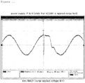
- Fig. 10 is an actual manufactured product of a surge protection device including a discharge element having a discharge-control electrode and a discharge-control circuit thereof according to the present invention, and a surge and voltage overlap test has been performed using a surge protection device of Fig. 10 , and as a result, it is seen that the surge protection device is not tripped even when a surge of 4 kV is applied in a state where AC 220 V has been applied, and the maximum voltage has a very low value as 464 V.
- Fig. 11 is an example of measuring a surge test result of the surge protection device of Fig. 10 .
Landscapes
- Emergency Protection Circuit Devices (AREA)
- Gas-Filled Discharge Tubes (AREA)
- Lasers (AREA)
Description
- The present invention relates to a new discharge element having a discharge-control electrode for inducing a discharge even at low voltage by improving a characteristic in which a discharge element may not be discharged against a fast transient voltage when it is at low voltage, and a driving circuit for driving a discharge element according to the present invention.
-
Fig. 1 illustrates a 2-pole discharge element in the prior art, and the element includesdischarge electrode 1 anddischarge electrode 2 at both ends of a cylindrical tube made of a ceramic insulator, and a discharge gap is formed inside the tube, and it has a structure filled with a discharge-assisting material (gas) inside the discharge gap. - In a discharge element as described above, when high voltage is applied between
discharge electrode 1 anddischarge electrode 2, a discharge-assisting material filled in the discharge gap starts a glow discharge while being ionized, and immediately it is followed by an ark discharge when a discharge current becomes large by the glow discharge, and thus a voltage applied between the discharge electrodes is instantaneously discharged and vanished. -
Fig. 2 illustrates a 3-pole discharge element in the prior art, and the element includes earth electrode contacted with discharge-assisting material (gas),discharge electrode 1 anddischarge electrode 2 at both ends of a cylindrical tube made of a ceramic insulator, and a discharge gap is formed bydischarge electrode 1 anddischarge electrode 2, and it has a structure filled with a discharge-assisting material (gas) inside the discharge gap. - In a 3-pole discharge element of
Fig. 2 , when high voltage is applied between discharge electrode 1 -discharge electrode 2, discharge electrode 1 - earth electrode, or discharge electrode 2 - earth electrode, a discharge-assisting material filled therein starts a glow discharge while being ionized, and immediately it is followed by an ark discharge when a discharge current becomes large by the glow discharge, and thus a high voltage applied between the electrodes is instantaneously discharged and vanished. - As seen in
Figs. 1 and2 , in a conventional discharge element, all of electrodes constituting the discharge element are physically and electrically connected to discharge-assisting material filled therein. - The discharge element is a gas-filled relay tube in which the discharge-assisting material is gas or vacuum, and it has a discharge characteristic that the tube is discharged at a level of about 90 V against direct current or transient voltage having a slow rising speed, such as a level of 100 V/sec. However, when a fast transient voltage, such as a level of 1,000 V/ps, is applied, it has a discharge characteristic that the tube is not discharged at a level of 700 V or lower.
- On the basis of the discharge characteristic of a convention discharge element, the recommendation of ITU-T is a different regulation from that of ANSI/IEEE. For a discharge element used as a protection element of PSTN lines, the ITU-T recommends that the element should be discharged at a level of 600V or lower against a slow rising speed, such as 100 V/sec while regulations such as ANSI/IEEE 61000-4-5 and UL497 define a fast transient characteristic of 1.2 µs/50 µs, and therefore those regulations have a problem that cannot be compromised even among such international regulations.
- In a state of disorder that even international regulations for such fast applied transient voltages are not unified, it is reality that the discharge element firmly occupies its place as a surge protection element in the communication field.
- As an example, a UL-certified discharge element of EPCOS, 3P230-05, is discharged at 225 V for direct current, but is discharged at 850 V as a result of testing a fast transient waveform with IEC C62.41 standard.
- Accordingly, for a testing according to international regulations that protection elements based on PSTN should be discharged within 600 V in the ITU-T, discharge elements typically used against a characteristic of transient voltage which is quickly applied, such as an induced surge, are all inadequate, and it is reality that lightning damage cannot be prevented even when a terminal box or MDF protection plug is actually installed in a building.
- Although the discharge-type element is universally used as a protection element for general communication in RS-232, 422, 485, or the like as well as in the PSTN field, efforts for reducing residual voltage after discharge have been made by adding a multi-level protection circuit, such as double or triple protection, due to the limit of a discharge characteristic thereof.
- In order to solve the problem, an object of the present invention is to provide a low voltage discharge element having a residual voltage characteristic that can be discharged even at a low transient voltage against a surge having a fast transient voltage characteristic, and a circuit for driving a discharge element of the present invention.
- More specifically, there is provided a discharge element that is discharged at 100 V or lower when a fast transient voltage, i.e., IEC C62.41 standard surge waveform (1.2 µs/50 µs) is applied between two discharge electrodes facing to each other, and a circuit for effectively driving a discharge element of the present invention.
- Furthermore, another object of the invention is to provide a surge protection device having a discharge element of the present invention.
- A discharge element having a discharge-control electrode according to the present invention comprises an
airtight cylinder 120 formed with a ceramic insulation material, a pair of discharge electrodes 111,112 arranged for facing an end opening of theairtight cylinder 120, adischarge gap 140 formed between the pair of discharge electrodes 111,112, a discharge-assistingmaterial 130 filled inside theairtight cylinder 120, and a discharge-control electrode 150 in contact with theairtight cylinder 120 and physically separated from the discharge-assistingmaterial 130, wherein a discharge between the pair of discharge electrodes 111,112 is induced by a control voltage applied through the discharge-control electrode 150. - The discharge-
control electrode 150 may be formed with a metal line, metal foil or metal piece, and a metal material of the metal line, metal foil or metal piece and a ceramic insulation material that forms an outside of theairtight cylinder 120 are closely contacted (adhered) in a line or surface, and the discharge-control electrode 150 may be inserted into a ceramic insulation material that forms theairtight cylinder 120 to be drawn out to an outside terminal. - At this time, the discharge-
control electrode 150 may be a ring-type, U-type or Y-type metal line, a metal foil, or a metal piece, and furthermore, the discharge-control electrode 150 may be electrically connected with one or more metal lines, metal foils, or metal pieces to be drawn out to a single terminal. - The discharge element may further comprise an
earth electrode 113 that a through hole is formed between thedischarge gap 140 and theairtight cylinder 120 to be physically contacted with the discharge-assisting material. - A control circuit of a
discharge element 100 having a discharge-control electrode comprises ahigh voltage transformer 300, and alimiting element 200 for limiting current, wherein a terminal A of a pair of discharge electrodes in a discharge element having a discharge-control electrode is connected to aterminal 311 of the primary side of thehigh voltage transformer 300, and anotherterminal 312 of the primary side of thehigh voltage transformer 300 and aterminal 322 of the secondary side of thehigh voltage transformer 300 are connected to another terminal B of the pair of discharge electrodes, and another terminal 321 of the secondary side of thehigh voltage transformer 300 is connected to a terminal C of the discharge-control electrode in the discharge element, and thelimiting element 200 is provided between a terminal A of the discharge electrode and aterminal 311 of the primary side of thehigh voltage transformer 300, or thelimiting element 200 is provided between a terminal A of the discharge electrode and another terminal B of the discharge electrode. - The
limiting element 200 is preferably at least one of elements selected from zener diode, varistor, diode, capacitor, TVS (Transient Voltage Suppressor) and piezoelectric element. - The limiting
element 200 is preferably a LC resonant circuit, and this is derived from a self capacitance obtained by an element applicable to the limitingelement 200, and a reactance obtained by a high voltage transformer, and it can work very usefully in a high frequency circuit. - The
high voltage transformer 300 is preferably a piezoelectric transformer, and thehigh voltage transformer 300 is preferably boosted 10 through 100 times higher than a voltage applied to the primary side to increase the voltage. - A control circuit of a
discharge element 100 having a discharge-control electrode according to the present invention may be used as an element constituting a surge protection device, and provides an excellent discharge performance even against a low voltage applied at high speed, and provides a low residual voltage characteristic, thereby providing a surge protection device having a more excellent surge protection performance. - A discharge element having a discharge-control electrode and a control circuit of the discharge element according to the present invention is a new discharge element and a control circuit totally different from the prior art, which has an excellent discharge performance even at a low voltage applied at high speed, and has a low residual voltage characteristic.
- Furthermore, a lightning/surge protector having a discharge element having a discharge-control electrode and a discharge-control element according to the present invention may provide a low residual voltage characteristic that the equipment can sufficiently survive even at an induced surge, thereby perfectly protecting the equipment from lightning, as well as provide an opportunity for preparing for a ground of enabling the unification of various international regulations through providing a discharge element discharged at low voltage.
- The above and other objects, features and advantages of the present invention will become apparent from the following description of preferred embodiments given in conjunction with the accompanying drawings, in which:
-
Fig. 1 is a view illustrating a 2-pole discharge element in the prior art; -
Fig. 2 is a view illustrating a 3-pole discharge element in the prior art; -
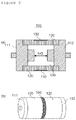
Fig. 3 is an embodiment of a discharge element having a discharge-control electrode according to the present invention; -
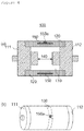
Fig. 4 is another embodiment of a discharge element having a discharge-control electrode according to the present invention; -
Fig. 5 is still another embodiment of a discharge element having a discharge-control electrode according to the present invention; -
Fig. 6 is still another embodiment of a discharge element having a discharge-control electrode according to the present invention; -
Fig. 7 is a view illustrating a characteristic of a discharge element in the prior art and a discharge element having a discharge-control electrode according to the present invention, andFig. 7A illustrates a 2-pole discharge element,Fig. 7B illustrates a 3-pole discharge element,Fig. 7C illustrates a 2-pole discharge element having a discharge-control electrode according to the present invention, andFig. 7D illustrates a 3-pole discharge element having a discharge-control electrode according to the present invention; -
Fig. 8 is an embodiment illustrating a driving circuit of a discharge element having a discharge-control electrode according to the present invention; -
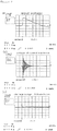
Fig. 9 is a result of measuring a characteristic of a discharge element and a control circuit thereof according to the present invention, andFig. 9A is a pulse waveform applied to an input as a standard surge waveform according to IEEE C62.41, which is a mixed waveform of 1.2µs/50µs and 8µs/20µs,Fig. 9B is a high voltage pulse applied to a discharge-control electrode of a discharge element according to the present invention, andFig. 9C is a result of discharge characteristic in which a pulse applied to an input is discharged and vanished by operation of a discharge element; -
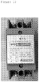
Fig. 10 is an actual manufactured product of a surge protection device having a discharge element and a control circuit thereof according to the present invention; and -
Fig. 11 is a surge test result measured by using a surge protection device ofFig. 10 . - 100: discharge element having discharge-control electrode
111,112: discharge-control electrode 120: ceramic insulator
130: discharge-assisting material (gas) 140: discharge gap
150,151,152: discharge-control electrode 113: earth electrode
200: limiting element 300: high voltage transformer - Hereinafter, a discharge element having a discharge-control electrode and a driving circuit for driving the discharge element according to the present invention will be described in detail with reference to accompanying drawings. The drawings illustrated below are provided as an example to fully convey the thought of the invention to those skilled in the art. Accordingly, the present invention is not limited to the drawings illustrated below, and may be realized by other alternative arrangements. Furthermore, the same reference numerals represent the same structural elements throughout the specification.
- Here, unless specifically defined otherwise, all technical or scientific terms used herein have the same meaning as commonly understood by those having ordinary skill in the art to which this invention belongs. In the following description and the attached drawings, the description of well-known functions and constructions which may unnecessarily obscure the gist of the invention will be omitted.
- A discharge element having a discharge-control electrode according to the present invention, as illustrated in
Fig. 3 , includes anairtight cylinder 120 formed with a ceramic insulation material, a pair of discharge electrodes 111,112 arranged for facing an end opening of theairtight cylinder 120, adischarge gap 140 formed between the pair of discharge electrodes 111,112, a discharge-assistingmaterial 130 filled inside theairtight cylinder 120, and a discharge-control electrode 150 in contact with theairtight cylinder 120 and physically separated from the discharge-assistingmaterial 130, wherein a discharge between the pair of discharge electrodes 111,112 is induced by a control voltage applied through the discharge-control electrode 150. - In the embodiment of
Fig. 3 , there is illustrated an example that a ring-type discharge-control electrode 150 made of a metal foil is formed on an outer surface of theairtight cylinder 120, and the outside of theairtight cylinder 120 formed with the discharge-control electrode 150 is engraved not to form a step profile by the discharge-control electrode 150 on the outer surface, however, the discharge-control electrode 150 according to the present invention may be made by approaching and pressing a U-type or Y-type metal body to the outer surface of theairtight cylinder 120, and may be a winding-type metal body. - The discharge-
control electrode 150 may be formed such that it is made of a metal line, metal foil or metal piece, and a metal material of the metal line, metal foil, or metal piece and a ceramic insulation material that forms an outside of theairtight cylinder 120 are contacted in a line or surface. The discharge-control electrode 150, as illustrated inFig. 4 , may be formed such that it is inserted into a ceramic insulation material that forms theairtight cylinder 120 to be drawn out to anoutside terminal 150a. - Furthermore, as illustrated in
Fig. 5 , one or more discharge-control electrodes 151,152 are formed, and each of the discharge-control electrodes 151,152 may be electrically connected with to be drawn out to a single terminal. - A thoughtful feature of the invention is to provide a discharge-control electrode that is completely separated and insulated, physically and electrically, when a surge (transient voltage) is not applied to an outside of a discharge gap in which two discharge electrodes are faced to each other, and thus a voltage higher than the voltage applied to a discharge electrode of the discharge-control electrode is created, when a very fast transient voltage is induced, to ionize a discharge-assisting material filled inside the discharge gap, thereby inducing a discharge between the discharge electrodes.
- The discharge-assisting material filled inside the discharge gap is preferably air, or a specific vacuum state, and typically a gas filled in the gas-filled relay tube may be used, and according to the characteristic it may be properly selected from gases, which do not belong to the 18th group (Ne, Ar, Kr, Xe, Rn) in the periodic table of elements, to be used.
- In addition, though an embodiment of a discharge tube having a discharge-control electrode according to the present invention has been described on the basis of a discharge element having a 2-pole structure as illustrated in
Figs. 3 through 5 , a gist of the invention may be applicable to a discharge element having a 3-pole structure as illustrated inFig. 6 . - Furthermore, though the discharge-control electrodes 151,152 of
Fig. 6 , as seen in a three-dimensional view ofFig. 6B , are not electrically connected in the discharge element itself, it is not connected to dischargeelectrodes earth electrode 113 and connected with one or more discharge-control electrodes 151,152 using a metal line. - A discharge element having a discharge-control electrode of the invention by a thoughtful feature of the present invention may be represented by
Fig. 7C or Fig. 7D. Fig. 7A illustrates a 2-pole discharge element,Fig. 7B illustrates a 3-pole discharge element,Fig. 7C illustrates a 2-pole discharge element having a discharge-control electrode according to the present invention, andFig. 7D illustrates a 3-pole discharge element having a discharge-control electrode according to the present invention. As illustrated inFig. 7 , this invention is greatly different from a structure of the discharge element in the prior art, in case where a transient voltage is induced, a discharge is induced between the discharge electrodes or between a discharge electrode and an earth electrode through the discharge-control electrode, which is in a state that is electrically insulated from the discharge-assisting material when the transient voltage is not induced. - More specifically, according to the present invention, a discharge-assisting material is filled in an airtight cylinder, and a discharge-control electrode exists on an outside wall body in the airtight cylinder, and an insulation material exists between the discharge-control electrode and the discharge-assisting material filled inside the airtight cylinder.
- The gases such as Ne, Ar, Kr, Xe, Rn, which belong to the 18th group in the periodic table of elements, are called as inert or inactive gases, because an atom has its outermost shell fully filled with electrons and has a very low energy level. For example, in case of NH3, which is an active gas, its outermost shell is filled with electrons through a covalent bond, but its energy by the covalent bond is unstable, when compared with the energy of an inert gas, and therefore it is easily broken, relatively, thereby easily causing an electrochemical reaction. Most of active gases excluding the 18th group in the periodic table of elements may cause an electrochemical reaction due to the energy when they are located in an electric field, and it is commonly understood in physical chemistry that an inert gas located in an electric field easily causes an electrochemical reaction due to its energy produced by the electric field. Moreover, it is difficult for an electric field to pass through a metal, but it has a characteristic that passes through a material, such as ceramic contained in the airtight cylinder, without any resistance, and an inert gas in the airtight cylinder is easily activated by a high voltage applied to a discharge-control electrode in an outside of the airtight cylinder, and such a voltage applied to both electrodes starts to produce a weak glow discharge, thereby more activating the gas, and as a result, causing an ark discharge.
- Hereinafter, a control circuit for controlling a discharge element having a control electrode according to the present invention will be described in detail.
- The discharge element having a discharge-control electrode according to the present invention includes a
high voltage transformer 300, and a limitingelement 200 for limiting current, wherein a terminal A of a pair of discharge electrodes in a discharge element having a discharge-control electrode is connected to aterminal 311 of the primary side of thehigh voltage transformer 300, and anotherterminal 312 of the primary side of thehigh voltage transformer 300 and aterminal 322 of the secondary side of thehigh voltage transformer 300 are connected to another terminal B of the pair of discharge electrodes, and another terminal 321 of the secondary side of thehigh voltage transformer 300 is connected to a terminal C of the discharge-control electrode in the discharge element, and the limitingelement 200 is provided between a terminal A of the discharge electrode and aterminal 311 of the primary side of the high voltage transformer 300 (Fig. 8A ), or the limitingelement 200 is provided between a terminal A of the discharge electrode and another terminal B of the discharge electrode (Fig. 8B ). - As illustrated in
Fig. 8A , the limitingelement 200 is provided between a terminal A of the discharge electrode and aterminal 311 of the primary side of thehigh voltage transformer 300, and is preferably at least one of elements selected from zener diode, varistor, diode, capacitor, TVS (Transient Voltage Suppressor) and piezoelectric element. - As illustrated in
Fig. 8B , the limitingelement 200 is provided between a terminal A of the discharge electrode and another terminal B of the discharge electrode, and is preferably a LC resonant circuit. - A core thought of the present invention, on the basis of a voltage induced (applied) to discharge electrodes A, B in a discharge-control electrode C of a
discharge element 100 having the discharge-control electrode C, a voltage applied to the discharge electrodes A, B is boosted and applied to the discharge-control electrode C to ionize a discharge-assisting material, thereby inducing a discharge of the discharge electrode even when a low transient voltage is applied at high speed (several µs) between the discharge electrodes A-B. - As illustrated in
Fig. 8A , when it is provided by serially connecting with at least one of limitingelements 200 selected from zener diode, varistor, diode, capacitor, and TVS, it has a simple voltage/current limiting function, but when it is provided with a parallel type resonant circuit, a frequency characteristic of all driving circuits including thedischarge electrode 100 may be greatly improved. Here, it is conceived that a lightning impulse of IEEE C61.41 is 1.2 µs/50 µs, and observed that a center frequency of lightning surge is about 800 KHz when its frequency spectrum is analyzed, and considered that a ring wave frequency of the same regulation is 100 KHz, and with reference to the frequency spectrum of standard waveforms such as 5 µs/30 µs, and 10 µs/700 µs, it may be applied based on the frequency characteristic in which a control circuit of the invention will be used, but in this description, there is constructed a LC resonant circuit (LC filter) having a characteristic that current can be mostly passed in the vicinity of rising speed (1.2 µs). - The limiting
element 200 is preferably constructed with a piezoelectric element such as ceramic resonator. In this case, however, a resonant frequency of the ceramic resonator should be within the range of frequencies of the lightning impulse. - In case of a typical discharge element, when a surge voltage of 100 V having a rising speed of 5 µs is induced between an electrode A and the other electrode B, it cannot be discharged since a very low pulse is instantaneously induced between the discharge electrodes A-B.
- In a control circuit of the invention, as illustrated in
Fig. 8 , current flows through the limitingelement 200, and through aterminal 311 of the primary coil in thehigh voltage transformer 300, and through another terminal 312, and finally to a terminal B of the discharge element. - The secondary coil in the
high voltage transformer 300 preferably has the boosting ratio at least greater than 10 times, more preferably, greater than 10 times and less than 100 times. However, the boosting ratio is a determined value in a control circuit of the invention based on the rated voltage and power supply condition in Korea. Most preferably,high voltage transformer 300 should provide a boosted voltage to a discharge-control electrode of the invention in such a manner that does not induce a discharge under a typical power fluctuation, but induce a discharge under a fluctuation, which is caused by an abnormal transient voltage induced, such as an induced surge, and therefore it would be apparent that it should be determined by considering a level of typical fluctuation of power, based on the rated voltage, power supply condition, and service environment for each country. -
Fig. 9 is a result of measuring a discharge characteristic of a discharge element based on its induced voltage by using the discharge element having a discharge-control electrode and a control circuit thereof according to the present invention. The input pulse ofFig. 9A means a voltage applied to the primary side of high voltage transformer, and as a pulse waveform applied to an input, which is a standard surge waveform according to IEEE C62.41, there are mixed waveforms such as 1.2 µs/50 µs and 8 µs/20 µs, at that instant a voltage applied to the primary side exceeds 73 V, as seen inFig. 9B , the secondary voltage exceeds 2,000 V, and an electric field produced by the high voltage (secondary voltage) applied through a discharge-control electrode functions to fully ionize the discharge-assisting material filled in the discharge gap inside the insulation material. - As a result, when the discharge-assisting material inside the discharge gap is ionized, it is instantaneously discharged through the sequence of a corona discharge-ark discharge between electrodes A-B, and therefore the surge pulse applied to both electrodes will be disappeared in an instant, as illustrated in
Fig. 9C . The discharge characteristic, as illustrated inFig. 9C , is a waveform, which is immeasurable by the prior art, and it is seen that the excellence of the present invention has been experimentally proven. - The control circuit according to the present invention is applicable to a 3-pole discharge element by the prior art, thereby driving an earth electrode terminal as a discharge-control electrode.
- However, at this time, the discharge-control electrode (earth electrode) is exposed to the discharge-assisting material therein to accelerate a discharge in a direction of
contact point 322 for the discharge-control electrode (earth electrode) and the secondary coil in the high voltage transformer, and thus the discharge characteristic may be remarkably decreased by a phenomenon that an ionization of side A and symbol 321 is slowed down. -
Fig. 10 is an actual manufactured product of a surge protection device including a discharge element having a discharge-control electrode and a discharge-control circuit thereof according to the present invention, and a surge and voltage overlap test has been performed using a surge protection device ofFig. 10 , and as a result, it is seen that the surge protection device is not tripped even when a surge of 4 kV is applied in a state where AC 220 V has been applied, and the maximum voltage has a very low value as 464 V.Fig. 11 is an example of measuring a surge test result of the surge protection device ofFig. 10 . - As described above, though a preferred embodiment of the present invention has been described as an example in detail with reference to the accompanying drawing, the present invention will not be limited to the above embodiment, and various modifications and alterations may be made by those having an ordinary skill in the art without departing from scope of the invention.
Claims (10)
- A discharge element for surge protection, comprising: an airtight cylinder (120) formed with a ceramic insulation material, a pair of discharge electrodes (111, 112) arranged for facing an end opening of the airtight cylinder, a discharge gap formed between the pair of discharge electrodes (111, 112), a discharge-assisting material (130) filled inside the airtight cylinder, and a discharge-control electrode (150; 151, 152) in contact with the airtight cylinder and physically separated from the discharge-assisting material, and a control circuit comprising a high voltage transformer (300), wherein a terminal A of the pair of discharge electrodes (111, 112) having a discharge control electrode (150; 151, 152) is connected to a terminal of a primary side of the high voltage transformer (300), and another terminal of the primary side of the high voltage transformer (300) and a terminal of a secondary side of the high voltage transformer (300) is connected to another terminal B of the pair of discharge electrodes (111, 112), and another terminal of the secondary side of the high voltage transformer (300) is connected to a terminal C of the discharge control electrode (150; 151, 152) in the discharge element, wherein the discharge-control electrode (150; 151, 152) is formed with a metal line, metal foil or metal piece, and a metal material of the metal line, metal foil or metal piece and a ceramic insulation material that forms an outside of the airtight cylinder (120) are closely contacted in a line or surface, and a discharge between the pair of discharge electrodes (111, 112) is induced by a control voltage applied through the discharge-control electrode (150; 151, 152), wherein the discharge-control electrode (150; 151, 152) is adapted to receive a boosted voltage from the high voltage transformer (300) as a result of an abnormal transient voltage applied to the discharge electrode (111, 112).
- The discharge element according to claim 1, wherein the discharge-control electrode (150; 151, 152) is inserted into a ceramic insulation material that forms the airtight cylinder (120) to be drawn out to an outside terminal.
- The discharge element according to claim 1, wherein the discharge-control electrode (150; 151, 152) is a ring-type, U-type or Y-type metal line, a metal foil, or a metal piece.
- The discharge element according to claim 1, wherein the discharge-control electrode (150; 151, 152) is electrically connected with one or more metal lines, metal foils, or metal pieces to be drawn out to a single terminal.
- The discharge element according to claim 1, further comprising an earth electrode that a through hole is formed between the discharge gap and the airtight cylinder (120) to be physically contacted with the discharge-assisting material (130) .
- The discharge element according to claim 1, further comprising a limiting element (200) for limiting current,
wherein the limiting element (200) is provided between the terminal A of the discharge electrode (111, 112) and a terminal of the primary side of the high voltage transformer (300), or
the limiting element (200) is provided between the terminal A of the discharge electrode (111, 112) and the another terminal B of the discharge electrode (111, 112). - The discharge element according to claim 6, wherein the limiting element (200) is at least one of elements selected from zener diode, varistor, diode, capacitor, TVS (Transient Voltage Suppressor) and piezoelectric element.
- The discharge element according to claim 6, wherein the limiting element (200) is a LC resonant circuit.
- The discharge element according to claim 6, wherein the high voltage transformer (300) is a piezoelectric transformer.
- The discharge element according to claim 6, wherein the high voltage transformer (300) has a characteristic that a voltage thereof is boosted 10 through 100 times higher than a voltage applied to the primary side to increase the voltage.
Applications Claiming Priority (2)
| Application Number | Priority Date | Filing Date | Title |
|---|---|---|---|
| KR1020070086390A KR100817485B1 (en) | 2007-08-28 | 2007-08-28 | Discharge element with discharge control electrode and control circuit thereof |
| PCT/KR2008/005049 WO2009028881A2 (en) | 2007-08-28 | 2008-08-28 | Discharge element with discharge-control electrode and the control circuit thereof |
Publications (3)
| Publication Number | Publication Date |
|---|---|
| EP2195823A2 EP2195823A2 (en) | 2010-06-16 |
| EP2195823A4 EP2195823A4 (en) | 2012-04-18 |
| EP2195823B1 true EP2195823B1 (en) | 2017-12-20 |
Family
ID=39411941
Family Applications (1)
| Application Number | Title | Priority Date | Filing Date |
|---|---|---|---|
| EP08793552.4A Active EP2195823B1 (en) | 2007-08-28 | 2008-08-28 | Discharge element with discharge-control electrode and the control circuit thereof |
Country Status (9)
| Country | Link |
|---|---|
| US (1) | US8227989B2 (en) |
| EP (1) | EP2195823B1 (en) |
| JP (1) | JP4961024B2 (en) |
| KR (1) | KR100817485B1 (en) |
| CN (1) | CN101960555B (en) |
| AU (1) | AU2008293219B2 (en) |
| CA (1) | CA2697674C (en) |
| MX (1) | MX2010002320A (en) |
| WO (1) | WO2009028881A2 (en) |
Families Citing this family (14)
| Publication number | Priority date | Publication date | Assignee | Title |
|---|---|---|---|---|
| KR101000484B1 (en) | 2009-07-03 | 2010-12-14 | 한국폴리텍Iv대학 산학협력단 | Discharge element and control device having discharge control electrode |
| US8279573B2 (en) * | 2009-07-30 | 2012-10-02 | General Electric Company | Circuit protection device and system |
| KR101209275B1 (en) * | 2011-04-25 | 2012-12-10 | 한국전자통신연구원 | Surge protection apparatus and method using same |
| KR102156230B1 (en) * | 2013-10-24 | 2020-09-15 | 삼성전자주식회사 | Data storage device for forcibly discharging remaining voltage, method thereof, and data processing system having the same |
| KR101476977B1 (en) * | 2013-11-21 | 2014-12-29 | 주식회사 한국서지연구소 | Gate Control Arrestor device and driving circuit of GCA device |
| DE102014102459A1 (en) | 2014-02-25 | 2015-08-27 | Epcos Ag | Snubber |
| DE102014107409A1 (en) * | 2014-05-26 | 2015-11-26 | Phoenix Contact Gmbh & Co. Kg | Surge arresters |
| JP6657746B2 (en) * | 2015-10-09 | 2020-03-04 | 三菱マテリアル株式会社 | Discharge tube |
| JP6156473B2 (en) * | 2015-12-08 | 2017-07-05 | 三菱マテリアル株式会社 | Surge protective element |
| KR101936103B1 (en) | 2018-09-18 | 2019-04-03 | 주식회사 한국서지연구소 | Dual Class SURGE and EMP Protector |
| CN118888410A (en) | 2019-06-19 | 2024-11-01 | 伯恩斯公司 | Gas discharge tube with enhanced leakage path length to gap size ratio |
| WO2021174140A1 (en) | 2020-02-27 | 2021-09-02 | Bourns, Inc. | Devices and methods related to mov having modified edge |
| DE102020115169B4 (en) * | 2020-06-08 | 2026-02-05 | Tdk Electronics Ag | Surge arrester and circuit arrangement with surge arrester |
| EP4730577A1 (en) * | 2023-06-16 | 2026-04-22 | Mitsubishi Electric Corporation | High-speed input device and power control circuit |
Family Cites Families (24)
| Publication number | Priority date | Publication date | Assignee | Title |
|---|---|---|---|---|
| CH470752A (en) * | 1967-03-15 | 1969-03-31 | Patelhold Patentverwertung | Controllable high vacuum electron tube |
| GB2060244B (en) * | 1979-10-09 | 1983-09-14 | Matsushita Electronics Corp | High pressure sodium vapour lamp |
| JPS5790590U (en) * | 1980-11-26 | 1982-06-03 | ||
| JPS5935354A (en) * | 1982-08-23 | 1984-02-27 | Iwasaki Electric Co Ltd | high pressure metal vapor discharge lamp |
| JPS59108290A (en) * | 1982-12-10 | 1984-06-22 | 日本電信電話株式会社 | Arrester tube |
| JPH01268427A (en) * | 1988-04-18 | 1989-10-26 | Fuji Electric Co Ltd | Abnormal voltage suppressor |
| DE3833167A1 (en) * | 1988-09-27 | 1990-03-29 | Siemens Ag | GAS DISCHARGE SURGE ARRESTER |
| DE9004811U1 (en) * | 1990-04-27 | 1990-07-05 | Patent-Treuhand-Gesellschaft für elektrische Glühlampen mbH, 8000 München | High pressure discharge lamp |
| JPH06150829A (en) * | 1992-02-13 | 1994-05-31 | Tama Electric Co Ltd | Surge absorbing element |
| JPH0785946A (en) * | 1993-09-16 | 1995-03-31 | Noritake Co Ltd | Lightning arrester element |
| SG68587A1 (en) * | 1996-07-27 | 1999-11-16 | Singapore Productivity And Sta | An electronic ballast circuit |
| ATE294451T1 (en) * | 1999-04-29 | 2005-05-15 | Koninkl Philips Electronics Nv | METAL HALIDE LAMP |
| EP1104582B1 (en) * | 1999-06-16 | 2006-11-02 | Koninklijke Philips Electronics N.V. | High-pressure discharge lamp |
| JP2001210445A (en) | 2000-01-31 | 2001-08-03 | Tokin Corp | Chip type surge absorbing element and method of manufacturing the same |
| US6563265B1 (en) * | 2000-11-06 | 2003-05-13 | General Electric Company | Applying prealloyed powders as conducting members to arc tubes |
| US6774566B2 (en) * | 2001-09-19 | 2004-08-10 | Toshiba Lighting & Technology Corporation | High pressure discharge lamp and luminaire |
| US20050035700A1 (en) * | 2001-11-20 | 2005-02-17 | Hidetoshi Yano | Discharge lamp and illuminating device |
| DE60325677D1 (en) * | 2002-09-13 | 2009-02-26 | Panasonic Corp | Metal halide lamp with device for suppressing unwanted discharges |
| JP4204855B2 (en) * | 2002-12-03 | 2009-01-07 | 音羽電機工業株式会社 | Surge absorption device and surge absorption circuit |
| WO2004091060A1 (en) * | 2003-04-10 | 2004-10-21 | Okaya Electric Industries Co., Ltd. | Discharge tube and surge absorbing device |
| JP4247555B2 (en) | 2003-08-08 | 2009-04-02 | 岡谷電機産業株式会社 | Discharge type surge absorber |
| JP2005063700A (en) * | 2003-08-19 | 2005-03-10 | Canon Inc | Storage medium attaching / detaching device |
| JP4880904B2 (en) * | 2005-02-15 | 2012-02-22 | 新光電気工業株式会社 | Discharge tube |
| JP2006244794A (en) * | 2005-03-02 | 2006-09-14 | Okaya Electric Ind Co Ltd | Discharge tube |
-
2007
- 2007-08-28 KR KR1020070086390A patent/KR100817485B1/en active Active
-
2008
- 2008-08-28 CA CA2697674A patent/CA2697674C/en active Active
- 2008-08-28 WO PCT/KR2008/005049 patent/WO2009028881A2/en not_active Ceased
- 2008-08-28 JP JP2009554463A patent/JP4961024B2/en active Active
- 2008-08-28 CN CN2008801047328A patent/CN101960555B/en active Active
- 2008-08-28 US US12/532,693 patent/US8227989B2/en active Active
- 2008-08-28 EP EP08793552.4A patent/EP2195823B1/en active Active
- 2008-08-28 AU AU2008293219A patent/AU2008293219B2/en not_active Ceased
- 2008-08-28 MX MX2010002320A patent/MX2010002320A/en active IP Right Grant
Non-Patent Citations (1)
| Title |
|---|
| None * |
Also Published As
| Publication number | Publication date |
|---|---|
| EP2195823A4 (en) | 2012-04-18 |
| WO2009028881A3 (en) | 2009-04-23 |
| CN101960555B (en) | 2012-08-08 |
| EP2195823A2 (en) | 2010-06-16 |
| KR100817485B1 (en) | 2008-03-31 |
| US8227989B2 (en) | 2012-07-24 |
| US20100141166A1 (en) | 2010-06-10 |
| WO2009028881A2 (en) | 2009-03-05 |
| AU2008293219A1 (en) | 2009-03-05 |
| MX2010002320A (en) | 2010-07-02 |
| CN101960555A (en) | 2011-01-26 |
| AU2008293219B2 (en) | 2011-05-12 |
| WO2009028881A4 (en) | 2009-06-11 |
| CA2697674C (en) | 2013-02-26 |
| JP4961024B2 (en) | 2012-06-27 |
| JP2010521794A (en) | 2010-06-24 |
| CA2697674A1 (en) | 2009-03-05 |
Similar Documents
| Publication | Publication Date | Title |
|---|---|---|
| US8227989B2 (en) | Discharge element with discharge-control electrode and the control circuit thereof | |
| EA006836B1 (en) | Protecting medium voltage inductive coupler device from electric transients | |
| CN101378178A (en) | Multi-gap metal ceramic gas discharge tube with external trigger terminal | |
| CN104333350B (en) | Cable energy-storage multiplex high-voltage pulse generation apparatus | |
| KR101000484B1 (en) | Discharge element and control device having discharge control electrode | |
| CN107271875A (en) | The pressure resistant testing device of voltage generation circuit and gas-insulating and fully-enclosed combined electrical apparatus | |
| CN201118096Y (en) | Multi-gap metal ceramic gas discharge tube with external trigger terminal | |
| Liljestrand et al. | Vacuum circuit breaker and transformer interaction in a cable system | |
| JP2004185982A (en) | Surge absorption device and surge absorption circuit | |
| CN216851297U (en) | Tripolar air gap type trigger device and surge protector | |
| Pham et al. | Empirical model of the impulse voltage-time characteristic of gas discharge tube | |
| JP4385104B2 (en) | Steep wave suppression device | |
| JP2024508921A (en) | Series static spark gap for EMP protection | |
| CN100468903C (en) | Three-electrode gap protection device for overvoltage protection system | |
| CN114243662B (en) | VFTO anti-interference circuit and switching device | |
| KR101476977B1 (en) | Gate Control Arrestor device and driving circuit of GCA device | |
| JP2745393B2 (en) | Discharge type surge absorbing element | |
| Kolyada et al. | The use of a magnetic switch for commutation of high-current pulse circuits | |
| Zamanillo et al. | Experimental study of the transfer of overvoltage surges through distribution transformers | |
| JP4385105B2 (en) | Discharge ignition device | |
| RU2208886C2 (en) | Overvoltage spark gap | |
| Lee | Improving breakdown voltage characteristics of GDAs using trigger voltage | |
| Burger et al. | Sources of transient electromagnetic disturbance in medium voltage switchgear | |
| Anji et al. | Voltage behavior of vacuum circuit breaker in case of series connected | |
| SU1647753A1 (en) | Snap-action device for protection of cable lines |
Legal Events
| Date | Code | Title | Description |
|---|---|---|---|
| PUAI | Public reference made under article 153(3) epc to a published international application that has entered the european phase |
Free format text: ORIGINAL CODE: 0009012 |
|
| 17P | Request for examination filed |
Effective date: 20100325 |
|
| AK | Designated contracting states |
Kind code of ref document: A2 Designated state(s): AT BE BG CH CY CZ DE DK EE ES FI FR GB GR HR HU IE IS IT LI LT LU LV MC MT NL NO PL PT RO SE SI SK TR |
|
| AX | Request for extension of the european patent |
Extension state: AL BA MK RS |
|
| REG | Reference to a national code |
Ref country code: DE Ref legal event code: R079 Ref document number: 602008053438 Country of ref document: DE Free format text: PREVIOUS MAIN CLASS: H01J0061020000 Ipc: H01J0061540000 |
|
| A4 | Supplementary search report drawn up and despatched |
Effective date: 20120321 |
|
| RIC1 | Information provided on ipc code assigned before grant |
Ipc: H01T 2/02 20060101ALI20120315BHEP Ipc: H01J 61/54 20060101AFI20120315BHEP |
|
| DAX | Request for extension of the european patent (deleted) | ||
| 17Q | First examination report despatched |
Effective date: 20161012 |
|
| GRAP | Despatch of communication of intention to grant a patent |
Free format text: ORIGINAL CODE: EPIDOSNIGR1 |
|
| INTG | Intention to grant announced |
Effective date: 20170706 |
|
| GRAS | Grant fee paid |
Free format text: ORIGINAL CODE: EPIDOSNIGR3 |
|
| GRAA | (expected) grant |
Free format text: ORIGINAL CODE: 0009210 |
|
| AK | Designated contracting states |
Kind code of ref document: B1 Designated state(s): AT BE BG CH CY CZ DE DK EE ES FI FR GB GR HR HU IE IS IT LI LT LU LV MC MT NL NO PL PT RO SE SI SK TR |
|
| REG | Reference to a national code |
Ref country code: GB Ref legal event code: FG4D |
|
| REG | Reference to a national code |
Ref country code: CH Ref legal event code: EP |
|
| REG | Reference to a national code |
Ref country code: IE Ref legal event code: FG4D |
|
| REG | Reference to a national code |
Ref country code: CH Ref legal event code: NV Representative=s name: RENTSCH PARTNER AG, CH Ref country code: AT Ref legal event code: REF Ref document number: 957090 Country of ref document: AT Kind code of ref document: T Effective date: 20180115 |
|
| REG | Reference to a national code |
Ref country code: DE Ref legal event code: R096 Ref document number: 602008053438 Country of ref document: DE |
|
| REG | Reference to a national code |
Ref country code: NL Ref legal event code: MP Effective date: 20171220 |
|
| PG25 | Lapsed in a contracting state [announced via postgrant information from national office to epo] |
Ref country code: NO Free format text: LAPSE BECAUSE OF FAILURE TO SUBMIT A TRANSLATION OF THE DESCRIPTION OR TO PAY THE FEE WITHIN THE PRESCRIBED TIME-LIMIT Effective date: 20180320 Ref country code: FI Free format text: LAPSE BECAUSE OF FAILURE TO SUBMIT A TRANSLATION OF THE DESCRIPTION OR TO PAY THE FEE WITHIN THE PRESCRIBED TIME-LIMIT Effective date: 20171220 Ref country code: SE Free format text: LAPSE BECAUSE OF FAILURE TO SUBMIT A TRANSLATION OF THE DESCRIPTION OR TO PAY THE FEE WITHIN THE PRESCRIBED TIME-LIMIT Effective date: 20171220 Ref country code: LT Free format text: LAPSE BECAUSE OF FAILURE TO SUBMIT A TRANSLATION OF THE DESCRIPTION OR TO PAY THE FEE WITHIN THE PRESCRIBED TIME-LIMIT Effective date: 20171220 |
|
| REG | Reference to a national code |
Ref country code: LT Ref legal event code: MG4D |
|
| REG | Reference to a national code |
Ref country code: AT Ref legal event code: MK05 Ref document number: 957090 Country of ref document: AT Kind code of ref document: T Effective date: 20171220 |
|
| PG25 | Lapsed in a contracting state [announced via postgrant information from national office to epo] |
Ref country code: HR Free format text: LAPSE BECAUSE OF FAILURE TO SUBMIT A TRANSLATION OF THE DESCRIPTION OR TO PAY THE FEE WITHIN THE PRESCRIBED TIME-LIMIT Effective date: 20171220 Ref country code: BG Free format text: LAPSE BECAUSE OF FAILURE TO SUBMIT A TRANSLATION OF THE DESCRIPTION OR TO PAY THE FEE WITHIN THE PRESCRIBED TIME-LIMIT Effective date: 20180320 Ref country code: LV Free format text: LAPSE BECAUSE OF FAILURE TO SUBMIT A TRANSLATION OF THE DESCRIPTION OR TO PAY THE FEE WITHIN THE PRESCRIBED TIME-LIMIT Effective date: 20171220 Ref country code: GR Free format text: LAPSE BECAUSE OF FAILURE TO SUBMIT A TRANSLATION OF THE DESCRIPTION OR TO PAY THE FEE WITHIN THE PRESCRIBED TIME-LIMIT Effective date: 20180321 |
|
| PG25 | Lapsed in a contracting state [announced via postgrant information from national office to epo] |
Ref country code: NL Free format text: LAPSE BECAUSE OF FAILURE TO SUBMIT A TRANSLATION OF THE DESCRIPTION OR TO PAY THE FEE WITHIN THE PRESCRIBED TIME-LIMIT Effective date: 20171220 |
|
| REG | Reference to a national code |
Ref country code: FR Ref legal event code: PLFP Year of fee payment: 11 |
|
| PG25 | Lapsed in a contracting state [announced via postgrant information from national office to epo] |
Ref country code: CZ Free format text: LAPSE BECAUSE OF FAILURE TO SUBMIT A TRANSLATION OF THE DESCRIPTION OR TO PAY THE FEE WITHIN THE PRESCRIBED TIME-LIMIT Effective date: 20171220 Ref country code: SK Free format text: LAPSE BECAUSE OF FAILURE TO SUBMIT A TRANSLATION OF THE DESCRIPTION OR TO PAY THE FEE WITHIN THE PRESCRIBED TIME-LIMIT Effective date: 20171220 Ref country code: ES Free format text: LAPSE BECAUSE OF FAILURE TO SUBMIT A TRANSLATION OF THE DESCRIPTION OR TO PAY THE FEE WITHIN THE PRESCRIBED TIME-LIMIT Effective date: 20171220 Ref country code: CY Free format text: LAPSE BECAUSE OF FAILURE TO SUBMIT A TRANSLATION OF THE DESCRIPTION OR TO PAY THE FEE WITHIN THE PRESCRIBED TIME-LIMIT Effective date: 20171220 Ref country code: EE Free format text: LAPSE BECAUSE OF FAILURE TO SUBMIT A TRANSLATION OF THE DESCRIPTION OR TO PAY THE FEE WITHIN THE PRESCRIBED TIME-LIMIT Effective date: 20171220 |
|
| PG25 | Lapsed in a contracting state [announced via postgrant information from national office to epo] |
Ref country code: RO Free format text: LAPSE BECAUSE OF FAILURE TO SUBMIT A TRANSLATION OF THE DESCRIPTION OR TO PAY THE FEE WITHIN THE PRESCRIBED TIME-LIMIT Effective date: 20171220 Ref country code: IS Free format text: LAPSE BECAUSE OF FAILURE TO SUBMIT A TRANSLATION OF THE DESCRIPTION OR TO PAY THE FEE WITHIN THE PRESCRIBED TIME-LIMIT Effective date: 20180420 Ref country code: PL Free format text: LAPSE BECAUSE OF FAILURE TO SUBMIT A TRANSLATION OF THE DESCRIPTION OR TO PAY THE FEE WITHIN THE PRESCRIBED TIME-LIMIT Effective date: 20171220 Ref country code: AT Free format text: LAPSE BECAUSE OF FAILURE TO SUBMIT A TRANSLATION OF THE DESCRIPTION OR TO PAY THE FEE WITHIN THE PRESCRIBED TIME-LIMIT Effective date: 20171220 |
|
| REG | Reference to a national code |
Ref country code: DE Ref legal event code: R097 Ref document number: 602008053438 Country of ref document: DE |
|
| PLBE | No opposition filed within time limit |
Free format text: ORIGINAL CODE: 0009261 |
|
| STAA | Information on the status of an ep patent application or granted ep patent |
Free format text: STATUS: NO OPPOSITION FILED WITHIN TIME LIMIT |
|
| 26N | No opposition filed |
Effective date: 20180921 |
|
| PG25 | Lapsed in a contracting state [announced via postgrant information from national office to epo] |
Ref country code: DK Free format text: LAPSE BECAUSE OF FAILURE TO SUBMIT A TRANSLATION OF THE DESCRIPTION OR TO PAY THE FEE WITHIN THE PRESCRIBED TIME-LIMIT Effective date: 20171220 |
|
| PG25 | Lapsed in a contracting state [announced via postgrant information from national office to epo] |
Ref country code: SI Free format text: LAPSE BECAUSE OF FAILURE TO SUBMIT A TRANSLATION OF THE DESCRIPTION OR TO PAY THE FEE WITHIN THE PRESCRIBED TIME-LIMIT Effective date: 20171220 |
|
| PG25 | Lapsed in a contracting state [announced via postgrant information from national office to epo] |
Ref country code: MC Free format text: LAPSE BECAUSE OF FAILURE TO SUBMIT A TRANSLATION OF THE DESCRIPTION OR TO PAY THE FEE WITHIN THE PRESCRIBED TIME-LIMIT Effective date: 20171220 |
|
| PG25 | Lapsed in a contracting state [announced via postgrant information from national office to epo] |
Ref country code: LU Free format text: LAPSE BECAUSE OF NON-PAYMENT OF DUE FEES Effective date: 20180828 |
|
| REG | Reference to a national code |
Ref country code: BE Ref legal event code: MM Effective date: 20180831 |
|
| PG25 | Lapsed in a contracting state [announced via postgrant information from national office to epo] |
Ref country code: BE Free format text: LAPSE BECAUSE OF NON-PAYMENT OF DUE FEES Effective date: 20180831 |
|
| PG25 | Lapsed in a contracting state [announced via postgrant information from national office to epo] |
Ref country code: MT Free format text: LAPSE BECAUSE OF NON-PAYMENT OF DUE FEES Effective date: 20180828 |
|
| PG25 | Lapsed in a contracting state [announced via postgrant information from national office to epo] |
Ref country code: TR Free format text: LAPSE BECAUSE OF FAILURE TO SUBMIT A TRANSLATION OF THE DESCRIPTION OR TO PAY THE FEE WITHIN THE PRESCRIBED TIME-LIMIT Effective date: 20171220 |
|
| PG25 | Lapsed in a contracting state [announced via postgrant information from national office to epo] |
Ref country code: HU Free format text: LAPSE BECAUSE OF FAILURE TO SUBMIT A TRANSLATION OF THE DESCRIPTION OR TO PAY THE FEE WITHIN THE PRESCRIBED TIME-LIMIT; INVALID AB INITIO Effective date: 20080828 Ref country code: PT Free format text: LAPSE BECAUSE OF FAILURE TO SUBMIT A TRANSLATION OF THE DESCRIPTION OR TO PAY THE FEE WITHIN THE PRESCRIBED TIME-LIMIT Effective date: 20171220 |
|
| PG25 | Lapsed in a contracting state [announced via postgrant information from national office to epo] |
Ref country code: IE Free format text: LAPSE BECAUSE OF NON-PAYMENT OF DUE FEES Effective date: 20180828 |
|
| PGFP | Annual fee paid to national office [announced via postgrant information from national office to epo] |
Ref country code: DE Payment date: 20240722 Year of fee payment: 17 |
|
| PGFP | Annual fee paid to national office [announced via postgrant information from national office to epo] |
Ref country code: GB Payment date: 20240723 Year of fee payment: 17 |
|
| PGFP | Annual fee paid to national office [announced via postgrant information from national office to epo] |
Ref country code: FR Payment date: 20240723 Year of fee payment: 17 |
|
| PGFP | Annual fee paid to national office [announced via postgrant information from national office to epo] |
Ref country code: CH Payment date: 20240901 Year of fee payment: 17 |
|
| PGFP | Annual fee paid to national office [announced via postgrant information from national office to epo] |
Ref country code: IT Payment date: 20240729 Year of fee payment: 17 |
|
| REG | Reference to a national code |
Ref country code: DE Ref legal event code: R119 Ref document number: 602008053438 Country of ref document: DE |
|
| REG | Reference to a national code |
Ref country code: CH Ref legal event code: H13 Free format text: ST27 STATUS EVENT CODE: U-0-0-H10-H13 (AS PROVIDED BY THE NATIONAL OFFICE) Effective date: 20260324 |
|
| PG25 | Lapsed in a contracting state [announced via postgrant information from national office to epo] |
Ref country code: CH Free format text: LAPSE BECAUSE OF NON-PAYMENT OF DUE FEES Effective date: 20250831 |
|
| GBPC | Gb: european patent ceased through non-payment of renewal fee |
Effective date: 20250828 |