EP2195085B1 - Electromagnetic interference shielding in an implantable medical device - Google Patents
Electromagnetic interference shielding in an implantable medical device Download PDFInfo
- Publication number
- EP2195085B1 EP2195085B1 EP08827070A EP08827070A EP2195085B1 EP 2195085 B1 EP2195085 B1 EP 2195085B1 EP 08827070 A EP08827070 A EP 08827070A EP 08827070 A EP08827070 A EP 08827070A EP 2195085 B1 EP2195085 B1 EP 2195085B1
- Authority
- EP
- European Patent Office
- Prior art keywords
- emi shield
- metal layer
- operational circuitry
- imd
- canister
- Prior art date
- Legal status (The legal status is an assumption and is not a legal conclusion. Google has not performed a legal analysis and makes no representation as to the accuracy of the status listed.)
- Active
Links
Images


Classifications
-
- A—HUMAN NECESSITIES
- A61—MEDICAL OR VETERINARY SCIENCE; HYGIENE
- A61N—ELECTROTHERAPY; MAGNETOTHERAPY; RADIATION THERAPY; ULTRASOUND THERAPY
- A61N1/00—Electrotherapy; Circuits therefor
- A61N1/18—Applying electric currents by contact electrodes
- A61N1/32—Applying electric currents by contact electrodes alternating or intermittent currents
- A61N1/38—Applying electric currents by contact electrodes alternating or intermittent currents for producing shock effects
- A61N1/39—Heart defibrillators
- A61N1/3968—Constructional arrangements, e.g. casings
-
- A—HUMAN NECESSITIES
- A61—MEDICAL OR VETERINARY SCIENCE; HYGIENE
- A61N—ELECTROTHERAPY; MAGNETOTHERAPY; RADIATION THERAPY; ULTRASOUND THERAPY
- A61N1/00—Electrotherapy; Circuits therefor
- A61N1/18—Applying electric currents by contact electrodes
- A61N1/32—Applying electric currents by contact electrodes alternating or intermittent currents
- A61N1/36—Applying electric currents by contact electrodes alternating or intermittent currents for stimulation
- A61N1/372—Arrangements in connection with the implantation of stimulators
- A61N1/375—Constructional arrangements, e.g. casings
- A61N1/37512—Pacemakers
-
- A—HUMAN NECESSITIES
- A61—MEDICAL OR VETERINARY SCIENCE; HYGIENE
- A61N—ELECTROTHERAPY; MAGNETOTHERAPY; RADIATION THERAPY; ULTRASOUND THERAPY
- A61N1/00—Electrotherapy; Circuits therefor
- A61N1/18—Applying electric currents by contact electrodes
- A61N1/32—Applying electric currents by contact electrodes alternating or intermittent currents
- A61N1/36—Applying electric currents by contact electrodes alternating or intermittent currents for stimulation
- A61N1/362—Heart stimulators
- A61N1/37—Monitoring; Protecting
- A61N1/3718—Monitoring of or protection against external electromagnetic fields or currents
Definitions
- the present invention relates to the field of implantable medical devices. More particularly, the present invention relates to implantable medical devices that include internal shielding to prevent electromagnetic interference with circuitry contained in such devices.
- Implantable cardiac stimulus devices typically include control circuitry that is adapted to perform various functions such as sensing, communication and/or stimulus delivery. Such devices operate within a patient's body, and are subject to various sources of electromagnetic interference (EMI) including, for example, noise from other electrical devices inside or outside of the patient's body, power line noise, noise generated by the patient's body itself, and, for some devices, noise that the device itself generates.
- EMI electromagnetic interference
- implantable cardiac stimulus devices typically deliver electric pulses to regulate or correct cardiac activity, and their sensing algorithms are often configured to avoid capturing self-generated signals.
- ICDs implantable cardioverter defibrillators
- EP 1 704 894 discloses an active implantable medical device (AIMD) having a magnetic shield on its housing for shielding the interior of the device from magnetic fields originating outside the housing.
- the magnetic shield is created using a magnetic absorbing coating on the inner surface of the housing.
- the AIMD includes an area of the housing left without the magnetic shield, a magnetic window, adjacent to a magnetically actuated device located inside of the housing. The magnetic window permits activation of the magnetically actuated device.
- the present invention in an illustrative embodiment, includes an implantable medical device that includes operational circuitry contained in a housing.
- An EMI shield is disposed between the operational circuitry and the housing.
- the EMI shield in an illustrative embodiment, includes an inner conductive layer which is coupled to a reference voltage.
- the EMI shield also includes an outer conductive layer that is exposed on its outer surface to the interior of the housing.
- the inner and outer conductive layers which may be formed of conductive metals, for example, silver or copper, are separated by a dielectric layer.
- FIGS.1A-1B show respective subcutaneous and transvenous cardiac stimulus systems
- FIGS. 2A-2B show perspective and cross-sectional views of an EMI shield
- FIG. 3 is an exploded view of an implantable medical device illustrating the assembly of a canister, EMI shields, and operational circuitry including batteries and capacitors;
- FIGS. 4A-4C illustrate, in plan and partial sectional views, an illustrative embodiment of an EMI shield
- FIG. 4D is a partial sectional view showing an alternative construction to that shown in FIG. 4C ;
- FIG. 5 shows an oscilloscope output illustrating corona discharges when the design of FIGS. 2A-2B is used as an EMI shield during a simulated high voltage signal application;
- FIG. 6A illustrates, in perspective view, a PEEK insulating liner
- FIG. 6B shows an oscilloscope output illustrating corona discharges when the design of FIGS. 2A-2B is used with the insulating liner of FIG. 6A as an EMI shield during a simulated high voltage signal application;
- FIG. 7A illustrates, in perspective view, an EMI shield having varnish applied along the edges thereof
- FIG. 7B shows an oscilloscope output illustrating corona discharges when the varnished EMI shield of FIG. 7A is used as an EMI shield during a simulated high voltage signal application;
- FIG. 8A illustrates, in perspective view, a varnished canister
- FIG. 8B shows an oscilloscope output illustrating corona discharges when the design of FIGS. 2A-2B is used as an EMI shield inside the varnished canister of FIG. 8A during a simulated high voltage signal application;
- FIG. 9 shows an oscilloscope output illustrating corona discharges when the design of FIGS. 2A-2B is used as an EMI shield while adhered to a canister during a simulated high voltage signal application;
- FIG. 10 is a perspective view showing an illustrative embodiment including an EMI shield having metallized tape applied to the outside thereof;
- FIG. 11 illustrates, for comparison, a sectional view of the shield of FIGS. 2A-2B in contact with a canister in contrast to a section view of the shield of FIG. 10 in contact with a canister;
- FIG. 12 shows an oscilloscope output illustrating linear response when the EMI shield of FIG. 10 is used as a shield during a simulated high voltage pulse
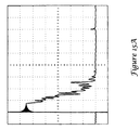
- FIGS. 13A-13B and 14A-14B show oscilloscope outputs comparing performance of an EMI shield as in FIGS. 2A-2B to that of an EMI shield as shown in FIG. 10 during delivery of simulated high voltage pulses;
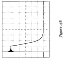
- FIGS. 15A-15B show oscilloscope outputs comparing performance of an EMI shield as shown in FIGS. 2A-2B to that of an EMI shield as shown in FIGS. 4A-4C ;
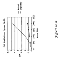
- FIGS. 16A-16B are graphs showing expected versus average detected currents for tested EMI shields.
- FIGS. 1A-1B respectively, show subcutaneous and transvenous implanted cardiac stimulus systems relative to the heart.
- the patient's heart 10 is shown in relation to an implanted, subcutaneous cardiac stimulus system including a canister 12.
- a lead 14 is secured to the canister and includes sensing electrode A 16, coil electrode 18, and sensing electrode B 20.
- a can electrode 22 is shown on the canister 12.
- Illustrative subcutaneous systems are shown in US Patent Numbers 6,647,292 and 6,721,597 , and the disclosures of these patents are incorporated herein by reference.
- Some embodiments include a unitary system having two or more electrodes on a housing as set forth in the '292 patent, rather than that which is shown in FIG. 1A .
- a unitary system including an additional lead may also be.used.
- the transvenous cardiac stimulus system includes a canister 32 connected to a lead 34.
- the lead 34 enters the patient's heart and includes electrodes A 36 and B 38. Additional electrodes for sensing or stimulus delivery may also be included, and also may be used for sensing in some embodiments of the present invention.
- electrode A 36 is located generally in the patient's ventricle
- electrode B 38 is located generally in the patient's atrium.
- the lead 34 may be anchored into the patient's myocardium.
- the lead 34 may also include one or more coil electrodes, either interior to or exterior to the heart, as shown at 42, which may be used to deliver stimulus and/or to sense cardiac or other activity, such as respiration.
- a can electrode 40 is shown on the canister 32. With this system, plural sensing vectors may be defined as well, in first and second polarities. In both FIGS. 1A and 1B , one or more sensing electrodes may also be used for stimulus delivery. Some embodiments of the present invention may be used in combination systems that may include sensing vectors defined between two subcutaneous electrodes, a subcutaneous electrode and a transvenous electrode, or two transvenous electrodes.
- the systems shown in FIGS. 1A-1B may include operational circuitry and a power source housed within the respective canisters.
- the power source may be, for example, a battery or bank of batteries.
- the operational circuitry may be configured to include such controllers, microcontrollers, logic devices, memory, and the like, as selected, needed, or desired for performing the illustrative methods set forth herein.
- the operational circuitry may (although not necessarily) further include a charging sub-circuit and a power storage sub-circuit (for example, a block of capacitors) for building up a stored voltage for cardiac stimulus taking the form of cardioversion and/or defibrillation pulses or stimuli.
- the operational circuitry may also be adapted to provide a pacing output.
- Both cardioversion/defibrillation and pacing sub-circuitry and capacities may be incorporated into a single device.
- Methods of signal analysis may be embodied in hardware within the operational circuitry and/or as instruction sets for operating the operational circuitry and/or in the form of machine-readable media (optical, electrical, magnetic, etc.) embodying such instructions and instruction sets.
- a cardioversion/defibrillation pulse may be supplied by a transvenous ICD in a variety of amplitudes, energy levels, and formats. Biphasic and monophasic waveforms can be used. Constant voltage or constant current formats may be used, though it is typical to provide an output that is "tilted,” that is, output voltage decays from an initial value over time as the energy storage circuit of the ICD discharges. Tilt is measured in terms of final voltage relative to initial voltage.
- an existing line of Medtronic® transvenous devices can be programmed to deliver initial output voltages of 83-736 volts with 0.4 to 30 Joules of delivered energy in a biphasic waveform with 50% tilt (assuming delivery into 75 ohms of resistance).
- voltages as low as 50 volts may be useful in some ICDs.
- Subcutaneous ICDs are being developed and are expected to utilize voltage outputs that will include at least the upper portions of the delivery energy and voltage ranges for transvenous devices, while also using higher delivery energies and voltages when necessary.
- delivery voltages in the range of 1350 volts, with energy in the range of 30-40 Joules, and up to 80 Joules, or more, are expected to be within the range of such devices, although higher and lower values may be realized. Electrode positioning can play a role in modifying such ranges. These values are merely illustrative and should not be taken as limiting.
- Each of the devices 12, 32 may further include such components as would be appropriate for communication (such as RF communication or inductive telemetry) with an external device such as a programmer.
- programmers 24 Figure 1A
- 42 Figure 1B
- the programmer 24, 42 may be used to activate and/or direct and/or observe diagnostic or operational tests.
- the programmer 24, 42 may be used to non-invasively determine the status and history of the implanted device.
- the programmer 24, 42 and the implanted device 12, 32 are adapted for wireless communication allowing interrogation of the implanted device.
- the programmers 24, 42 in combination with the implanted devices 12, 32 may also allow annunciation of statistics, errors, history and potential problem(s) to the user/physician.
- the particulars of operational circuitry, signal analysis, lead placement, implantation, communication and programmers may vary widely in embodiments associated with the present invention.
- FIGS. 2A-2B show a perspective and a cross-sectional view of an EMI shield.
- the shield 60 includes a solder pad 62 that allows soldering of a layer of the EMI shield to the ground plane of the associated circuitry.
- a relatively small patch-type pad may be placed over the solder pad 62 to electrically isolate it from an associated canister.
- a cross section of the EMI shield shows an outer dielectric layer 64, which covers a metal layer 66, which is placed on an inner dielectric layer 68.
- the dielectric layers 64, 68 include 25.4 ⁇ m (1 mil) of polyimide.
- the metallic layer 66 may be pulled back to reduce edge effects. Any conductive metal or alloy maybe used as metallic layer 66; in illustrative examples, copper and/or silver are used. In an illustrative example, the metallic layer 66 was pulled back 0.254mm (10 mils) from the edge of the EMI shield 60.
- the solder pad 62 was used to tie the metallic layer 66 to a reference voltage (i.e., ground) for the overall device. Certain shortcomings of this design are explained in further detail below.
- the EMI shield 60 is used by placing it between housed operational circuitry and a canister provided to house the operational circuitry, as shown by FIG. 3 .
- FIG. 3 is an exploded view of an implantable medical device illustrating the assembly of a canister, EMI shields, and operational circuitry including batteries and capacitors.
- the canister includes a first component 80 and a second component 82.
- the first and second components 80, 82 may be made of any suitable biocompatible material. Titanium is an illustrative material, although other materials may be used in place of or in combination with titanium. Portions of the outside of the first and second components 80, 82 may be coated, shaped, or treated in any suitable fashion. In some embodiments, the first and second components may be configured to matingly fit together, for example, in a snap fit or an overlapping fit.
- the completed device will have a weld seam joining the first component 80 to the second component 82, although additional intermediate members may also be included on the inside or outside of the device, and welding need not be used for some embodiments using, for example, adhesive or snap-fit.
- a first EMI shield portion 84 and a second EMI shield portion 86 Internal parts shown in the exploded view include a first EMI shield portion 84 and a second EMI shield portion 86.
- a solder pad is shown on the first EMI shield portion 84.
- Sandwiched between the EMI shield portions 84, 86 is the operational circuitry of the device.
- the operational circuitry is shown in a highly simplified fashion, and includes a capacitor block 88, control components 90, and a battery 92.
- the operational circuitry shown is likely for such devices as ICDs or other devices that provide electrical stimuli to a patient.
- the precise details of the control components and/or the operational circuitry generally may vary widely depending upon the desired functionality of the device.
- the operational circuitry will define a ground potential for operation of its circuitry.
- a reference output which may be the operational circuitry ground or some other voltage defined relative to the operational circuitry ground, may be electrically connected to the metal layer of an associated EMI shield at the solder pad.
- a frame (not shown) may be included to hold the operational circuitry parts 88, 90, 92, in place.
- FIG. 3 A number of the Figures that follow show oscilloscope outputs that were generated during actual testing of devices during simulated high voltage pulse delivery.
- the testing methods can be understood by viewing the exploded view of FIG. 3 .
- the illustrative tests referred to in the Figures which follow were performed by providing one of the EMI shield portions 84, 86 against a corresponding canister component 80, 82. Substitutes for the relatively expensive operational circuitry components that would be used in an actual device were provided, including a non- functional battery, capacitors and an associated frame that would be used in an actual device to hold the operational circuitry together in place within the canister.
- FIGS. 6B , 7B , 8B , 9 , 12 , 13A-13B and 14A-14B testing was performed using a 60-Hz output.
- the oscilloscope views in these Figures were captured with an applied signal of 1000 Vrms. Nonlinearities caused by corona discharge show up as spikes on the oscilloscope outputs. Actual measurement of the amount of current caused by the corona discharge was calculated by monitoring the voltage across a series 10 kilo0nm resistor. This form of simulation of high voltage pulse delivery is believed to provide a reasonable and useful understanding of whether and how well the proposed EMI shields performed with respect to corona discharge.
- FIGS. 4A-4C show, in plan and partial sectional views, an illustrative embodiment of an EMI shield.
- the EMI shield is shown generally at 100, and is designed to have first and second components connected by a narrow bridge member, allowing it to fold around operational circuitry.
- the EMI shield 100 may be fabricated in any manner allowing for the multi-layered constructions described herein.
- the EMI shield 100 may be manufactured as a flexible printed circuit board.
- the canister for the implantable medical device includes first and second major faces, with the EMI shield 100 shaped as shown to correspond to the major face(s) of the device. In other embodiments, the EMI shield 100 may be shaped as desired.
- conformal ICDs are shown in US Patent Number 6,647,292 , having longer, curved housings; an EMI shield 100 may be shaped or formed differently for such applications.
- the EMI shield 100 may also be sized to cover only a desired region of the implantable medical device.
- FIG. 4B highlights details around a solder pad 120 in the EMI shield 100 in FIG. 4A .
- the details of the illustrative EMI shield 100 that are shown in FIG. 4B away from the solder pad 120 may be consistent with the rest of the EMI shield 100 except for its edges.
- a first dielectric layer 102 has an outer metal layer 104 thereon.
- the first dielectric is polyimide, though other dielectric materials may be used.
- An inner metal layer 106 is secured to the first dielectric layer 102. The exact construction may vary, for example, depending upon the manner of fabrication used.
- the EMI shield 100 may be constructed of separate layers that are assembled together using adhesives; in other embodiments, the EMI shield 100 may be formed by deposition processes.
- the metal layers 104, 106 are formed/placed on the first dielectric layer 102 in a process forming a flexible printed circuit board. If desired, the entire device may be made in such a manner, including the additional second dielectric layer 110.
- a second dielectric layer 110 is also provided inside of the inner metal layer 106 to isolate housed operational circuitry from undesired or inadvertent contact with the inner metal layer, which may be coupled to a reference output or ground of the housed operational circuitry. While the second dielectric layer 110 may be omitted in some embodiments, it will often serve to reduce or limit cross talk and/or inadvertent shorting of sub-circuits in the device by covering some, a majority, or nearly all of the inner metal layer 106.
- the second dielectric layer 110 is ESPANEXTM SPC-35A-25A, a laminate-ready commercially available polyimide coverlay with an adhesive 108 already provided thereon, allowing it to bond to the inner metal layer 106.
- Other dielectric materials may be used.
- the metal layers 104, 106 may be formed of any suitable conductive metal, such as silver, copper, etc., and may be selected in view of various factors such as durability, cost, resistance to corrosion, ease of manufacture, bonding or handling, and biocompatibility, for example.
- FIG. 4B also shows that at the solder pad 120, the outer metal layer 104 may be pulled back such that it is separated from the portion 112 of the inner metal layer 106 that is provided to allow secure soldering.
- a suitable connection such as a conductive wire, can be soldered from the operational circuitry to the solder pad 120, allowing the inner metal layer 106 to be grounded.
- the exposed portion 112 of the inner metal layer that extends across the first dielectric layer 102 can be covered, after soldering, with an additional dielectric patch before placing a canister thereover.
- FIG. 4C illustrates a perimeter portion of the EMI shield 100.
- the outer metal layer 104 extends virtually to the edge of the perimeter portion, while the inner metal layer 106 ends a distance away from the edge, defining a pull-back region along the perimeter.
- the pull-back region may have a width of from about 25.4 ⁇ m (1 mil) to about 25.4 mm (100 mils) for example.
- the dielectric layers 102, 110 may have thicknesses in the range of about 25.4-254 ⁇ m (1-10 mils) 8, although this may vary. In an illustrative embodiment further discussed below, the dielectric layers 102, 110 are about 50.8 ⁇ m (2 mils) thick, and the inner metal layer 106 is pulled back about 1.52 mm (60 mils) from the edge of the EMI shield 100.
- FIG. 4D is a partial sectional view showing an alternative construction to that shown in FIG. 4C .
- an EMI shield 130 includes an outer metal layer 132 having a portion that extends around the edge of the shield, as shown at 134. Again, the inner metal layer 138 is shown ending a distance away from the edge of the perimeter of the EMI shield 130.
- An adhesive 144 may be used to secure the inner metal layer 138 to a second dielectric layer 142, as well as to join the first dielectric layer 136 and second dielectric layer 142 in the pull-back region 140 between the perimeter of the EMI shield 130 and the outer perimeter of the inner metal layer 138 and the edge of the perimeter of the EMI shield 130.
- the dielectric layers 136, 142 may have differing thicknesses, as shown.
- the edge of the EMI shield may be exposed to the interior of the canister.
- extending the outer metal layer 132 to wrap around the edge of the perimeter of the EMI shield 130, as shown at 134 provides an additional "touch-point" for touching the outer metal layer 132 to the canister (see FIG. 3 ).
- the "air gap" which is further explained below, can be eliminated along this portion of the device.
- the provision of one or more touch points between the conductive outer metal layer 132 and the canister may aid in reducing corona discharge.
- FIG. 5 shows an oscilloscope output illustrating corona discharge when the EMI shield of FIGS. 2A-2B is used as a shield during a simulated high voltage pulse.
- the testing methods used applied a 60-Hz sinusoidal signal.
- a problem with the waveform in FIG. 5 is the nonlinearities that are visible at 190, 192. These spikes 190, 192 are caused by corona discharges that occur across the air gaps between the outer dielectric layer 64 ( FIG. 2B ) of the EMI shield and the interior of the canister. These corona discharges can become large enough to be visualized as sparks along the outside edge of the EMI shield under the right circumstances.
- the corona discharge may be the cause of at least some system resets, as well as other electronics problems that occur during testing of ICDs using the shield shown in FIGS. 2A-2B .
- the above described testing setup and procedure was used prior to applying a signal.
- the capacitance of the testing structure was determined using a commercially available device for testing capacitance.
- an expected current was determined. Actual current was then monitored during testing. Comparing the actual current to the expected current provides an estimate of the effectiveness of the EMI shield in preventing corona discharges.
- the results for the EMI shield of FIGS. 2A-2B showed individual corona discharges of up to 1.5 mA, and a difference between average and expected RMS current of about 0.6 mA rms at 1000 Vrms, meaning that the average current about tripled the expected current.
- the oscilloscope output shown in FIG. 5 clearly shows large spikes resulting from corona discharges occurring at and near the signal peaks. In testing, nonlinearities could be detected at voltages as low as 300 Vrms.
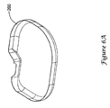
- FIG. 6A illustrates, in a perspective view, a PEEK insulating liner 200.
- the PEEK liner 200 is about 101.6 ⁇ m (4 mils) thick, and is shaped to be placed between an EMI shield as shown in FIGS. 2A-2B and a canister for an implantable medical device.
- FIG. 6B shows the oscilloscope output for the instantaneous current using the PEEK liner 200 in addition to an EMI shield as in FIGS. 2A-2B .
- the scale is the same in FIG. 6B as in FIG. 5 .
- the average current was greatly reduced by the addition of more insulation. However, current spikes from corona discharge are also clearly visible.
- the difference between average and expected current is in the range of 0.023 mA rms, and corona discharges of up to 0.5 mA were identified.
- the increase in average current was in the range of 20% relative to expected current.
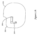
- FIG. 7A illustrates, in perspective view, an EMI shield 210 having varnish 212 applied to the outer edges thereof, and varnish 216 applied around solder pad 214.
- the applied varnish 212, 216 was an insulating varnish with an insulating strength in the range of 39 kv/mm (1000V/mil).
- a strong out-of-phase current resulted at 1000 Vrms, with relatively large and frequent corona discharge for the EMI shield of FIG. 7A .
- a difference of 0.82 mA rms between expected and average current resulted, nearly tripling the current, with spikes as large as 0.7 mA.
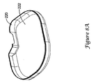
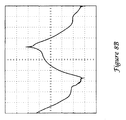
- FIG. 8A illustrates, in perspective view, a varnished canister.
- the varnish 222 was applied to the entire interior of the can 220. Again, the applied varnish was an insulating varnish with an insulating strength in the range of about 39 kv/mm (1000V/mil).
- the varnished canister again provided a strong out-of-phase component, with corona discharge still occurring, although with less amplitude and frequency.
- the difference between average and expected current was about 0.39 mA rms, nearly tripling the expected current, with spikes as large as 0.3 mA. Full insulation on the can reduced corona, but did not eliminate it.
- FIG. 9 shows an oscilloscope output illustrating corona discharge when the EMI shield of FIGS. 2A-2B is used as a shield while adhered to a canister during a simulated high voltage pulse.
- adhesive was applied to the interior of a canister, and the EMI shield was placed therein, with the aim of reducing and/or eliminating air gaps across which corona discharge formed in the above tests.
- the difference between expected and average current was about 0.186 mA rms, representing a change of around 20%, with individual discharge spikes as large as 0.4 mA.
- Corona discharges were still present with adhesive, but they were greatly reduced simply by bonding the shield to the can. Since this adhesive only covered approximately 75% of the shield surface area, it was not fully effective.
- FIG. 10 is a perspective view showing an illustrative embodiment of the present invention including an EMI shield 240 having metal tape 242 applied to the outside thereof.
- the aim was to eliminate air gaps having large voltages across them.
- the metallized tape 242 would conduct electricity from the can to itself, eliminating voltage across air gaps between the EMI shield 240 and the outer can. Because it was adhered first to the EMI shield 240, the metallized tape 242 would not introduce additional air gaps between its metal and the metal layer of the EMI shield 240, placing the voltage across only the dielectric.
- the dielectric would now include the polyimide layer and any adhesives between the EMI shield 240 metal layer and the metal layer on the metal tape 242.
- FIG. 11 provides an exaggerated illustration comparing a sectional view of a shield 250 as in FIGS. 2A-2B in contact with a canister 252 to a sectional view of a shield 260 as in FIG. 10 in contact with a canister 266.
- an air gap is seen between the shield 250 (which includes exaggerated curvature) and the canister 252. Supposing an applied 1400-volt pulse, the potential across the air gap would be about 1400 volts, possibly enough to induce breakdown such as corona discharge, depending upon humidity, temperature, and the size of the gap.
- the surface of the EMI shield 250 formed by the dielectric will have a voltage gradient due to its high resistivity. The contact between the EMI shield 250 and the canister 252 does not eliminate the voltage across air gaps.
- the other EMI shield 260 includes an inner metal layer 262, a dielectric 263, and an outer metal layer 264. As shown at 268, air gaps may also occur with the EMI shield 260. However, the conductivity of the outer metal layer 264 eliminates the voltage potential across the air gap. The voltage gradient across the surface of the metal layer will be minimal compared to that of the dielectric surface on the other EMI shield 250. The "touch points" that surround the air gap at 268 short the voltage across the air gap, preventing corona discharge.
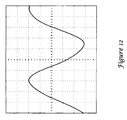
- FIG. 12 shows an oscilloscope output illustrating linear response when the EMI shield of FIG. 10 is used with high voltage applied.
- the results in FIG. 12 show substantial elimination of the corona discharge.
- the difference between average and expected current at 1000 Vrms was about 0.07 mA rms.
- Current spikes of individual discharges were not detectable on the same scale as the other designs; changing the scale of the oscilloscope showed infrequent current spikes of less than 0.06 mA.
- This prototype EMI shield used metallized tape, and was rather rough in its execution (i.e., there may have been gaps between tape pieces, flaws in the insulation due to handling, and the tape may not have bonded perfectly, leaving internal air gaps, etc.). It was expected that further refinement, for example, construction of the EMI shield as shown in FIGS. 4A-4C , would improve performance.
- Another prototype having the metallized tape was prepared, this time using an EMI shield having double the insulation (50.8 ⁇ m (2 mils) of polyimide instead of 25.4 ⁇ m (1 mil)) and including a metal layer pulled back 1.52 mm (60 mils), rather than 0.254 mm (10 mils) from the edges.
- the frequency and amplitude of corona discharges was greatly reduced.
- the average current was reduced from 0.6 mA rms to 0.016 mA rms (1/38 th ) and maximum corona amplitudes reduced from 1.5 mA to .03 mA (1/50 th ).
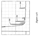
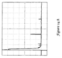
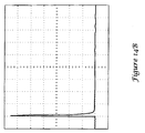
- FIGS. 13A-13B and 14A-14B show oscilloscope outputs comparing the performance of a shield as in FIGS. 2A-2B to that of a shield having doubled insulation (50.8 ⁇ m (2 mils) of polyimide), with an inner metal layer pulled back 1.52 mm (60 mils) (as compared to 0.254 mm (10 mils)) and including metallized tape on the outside. This time, high voltage pulses were tested.
- FIG. 13A shows the oscilloscope for a 1350-volt shock waveform using the EMI shield of FIGS. 2A-2B . Large spikes are clearly shown at 300, 302, and even at 304, with a peak amplitude of the corona discharges being in the range of 80 mA.
- FIG. 13B which uses the same scale as FIG. 13A , no corona discharge spikes are seen with the EMI shield having doubled insulation, a larger pull-back region, and metal tape.
- FIGS. 14A-14B A broader scale is shown in FIGS. 14A-14B , further highlighting the differences in performance.
- EMI shields (three of each of the two types) were tested. The testing involved using an external power supply for the system, but the internal control circuitry for an implantable cardioverter defibrillator was powered and active during shock delivery, in order to observe whether the control system reset during the shock delivery. Telemetry was also performed to assess the effect of the EMI shields on the rate of framing errors that occurred during telemetry communications.
- FIG. 15A shows the oscilloscope output for one of the shocks delivered with the shield of FIGS. 2A-2B , and includes significant apparent corona discharge effects.
- control circuitry in devices having the shields as shown in FIGS. 4A-4C using amplitudes in the same range of 1380 volts, did not reset a single time during 231 tests (0/80, 0/80 and 0/71 for the three prepared EMI shields). Testing used the same three sets of circuitry for both series of tests, in order to show that the shields themselves, rather than the circuitry, caused the difference in performance.
- FIG. 15B shows the oscilloscope output for one of the shocks delivered with the shield of FIGS. 4A-4C in place, and does not include the corona discharge effects seen with the other shield.
- the metal tape prototype testing was further confirmed.
- corona discharge was apparent in response to applied 60-Hz sinusoid at 1000 Vrms and 2000 Vrms, with spikes as large as 2 mA, and with corona discharge appearing at applied voltages exceeding 240 Vrms.
- Spiking was not detected for the EMI shields as shown in FIGS. 4A-4C in response to an applied 60-Hz sinusoid at 1000 Vrms, with testing including observation at scales that would show spikes as small as 0.01 mA.
- the EMI shields as shown in FIGS. 4A-4C allowed current spikes in the range of 0.03 mA in amplitude, with these relatively small current spikes being first observed at around 1050 Vrms.
- FIG. 16A shows results for expected versus average current with the EMI shields as shown in FIGS. 2A-2B for three tested EMI shields. Significant deviation from the expected current occurred for these EMI shields.
- FIG. 16B shows results for EMI shields as shown in FIGS. 4A-4C on the same scale used in FIG. 16A . In contrast to the other EMI shields, minimal deviation occurs, indicating very limited corona discharge.
Landscapes
- Health & Medical Sciences (AREA)
- Life Sciences & Earth Sciences (AREA)
- Animal Behavior & Ethology (AREA)
- Nuclear Medicine, Radiotherapy & Molecular Imaging (AREA)
- Radiology & Medical Imaging (AREA)
- Biomedical Technology (AREA)
- Engineering & Computer Science (AREA)
- General Health & Medical Sciences (AREA)
- Public Health (AREA)
- Veterinary Medicine (AREA)
- Heart & Thoracic Surgery (AREA)
- Cardiology (AREA)
- Biophysics (AREA)
- Electrotherapy Devices (AREA)
- Shielding Devices Or Components To Electric Or Magnetic Fields (AREA)
Applications Claiming Priority (2)
| Application Number | Priority Date | Filing Date | Title |
|---|---|---|---|
| US11/833,987 US7769457B2 (en) | 2007-08-04 | 2007-08-04 | Electromagnetic interference shielding in an implantable medical device |
| PCT/US2008/071972 WO2009020871A1 (en) | 2007-08-04 | 2008-08-01 | Electromagnetic interference shielding in an implantable medical device |
Publications (2)
| Publication Number | Publication Date |
|---|---|
| EP2195085A1 EP2195085A1 (en) | 2010-06-16 |
| EP2195085B1 true EP2195085B1 (en) | 2011-11-09 |
Family
ID=39816890
Family Applications (1)
| Application Number | Title | Priority Date | Filing Date |
|---|---|---|---|
| EP08827070A Active EP2195085B1 (en) | 2007-08-04 | 2008-08-01 | Electromagnetic interference shielding in an implantable medical device |
Country Status (9)
| Country | Link |
|---|---|
| US (4) | US7769457B2 (enExample) |
| EP (1) | EP2195085B1 (enExample) |
| JP (1) | JP5280446B2 (enExample) |
| CN (1) | CN101896222B (enExample) |
| AT (1) | ATE532557T1 (enExample) |
| AU (1) | AU2008284051B2 (enExample) |
| CA (1) | CA2695508C (enExample) |
| ES (1) | ES2376027T3 (enExample) |
| WO (1) | WO2009020871A1 (enExample) |
Families Citing this family (34)
| Publication number | Priority date | Publication date | Assignee | Title |
|---|---|---|---|---|
| US7769457B2 (en) * | 2007-08-04 | 2010-08-03 | Cameron Health, Inc. | Electromagnetic interference shielding in an implantable medical device |
| US10080889B2 (en) | 2009-03-19 | 2018-09-25 | Greatbatch Ltd. | Low inductance and low resistance hermetically sealed filtered feedthrough for an AIMD |
| US8126170B2 (en) * | 2008-09-05 | 2012-02-28 | Apple Inc. | Electromagnetic interference shields with piezos |
| US8265329B2 (en) * | 2008-09-05 | 2012-09-11 | Apple Inc. | Compact housing for portable electronic device with internal speaker |
| US20120256704A1 (en) * | 2011-03-01 | 2012-10-11 | Greatbatch Ltd. | Rf filter for an active medical device (amd) for handling high rf power induced in an associated implanted lead from an external rf field |
| US20100246143A1 (en) * | 2009-03-26 | 2010-09-30 | Richard Hung Minh Dinh | Electromagnetic Interference Shielding for Compact Electronic Devices |
| ES2584959T3 (es) | 2009-12-31 | 2016-09-30 | Cardiac Pacemakers, Inc. | Dispositivo implantable incluyendo una batería reductora de corrientes parásitas |
| WO2011082223A1 (en) * | 2009-12-31 | 2011-07-07 | Cardiac Pacemakers, Inc. | Implantable device including eddy current reducing capacitor |
| US8548573B2 (en) * | 2010-01-18 | 2013-10-01 | Cameron Health, Inc. | Dynamically filtered beat detection in an implantable cardiac device |
| US9030159B2 (en) | 2010-03-26 | 2015-05-12 | Boston Scientific Neuromodulation Corporation | Inductive charger with magnetic shielding |
| US9974944B2 (en) | 2010-07-29 | 2018-05-22 | Cameron Health, Inc. | Subcutaneous leads and methods of implant and explant |
| US11198014B2 (en) | 2011-03-01 | 2021-12-14 | Greatbatch Ltd. | Hermetically sealed filtered feedthrough assembly having a capacitor with an oxide resistant electrical connection to an active implantable medical device housing |
| US10596369B2 (en) | 2011-03-01 | 2020-03-24 | Greatbatch Ltd. | Low equivalent series resistance RF filter for an active implantable medical device |
| US9931514B2 (en) | 2013-06-30 | 2018-04-03 | Greatbatch Ltd. | Low impedance oxide resistant grounded capacitor for an AIMD |
| US10350421B2 (en) | 2013-06-30 | 2019-07-16 | Greatbatch Ltd. | Metallurgically bonded gold pocket pad for grounding an EMI filter to a hermetic terminal for an active implantable medical device |
| US9427596B2 (en) | 2013-01-16 | 2016-08-30 | Greatbatch Ltd. | Low impedance oxide resistant grounded capacitor for an AIMD |
| US10272252B2 (en) | 2016-11-08 | 2019-04-30 | Greatbatch Ltd. | Hermetic terminal for an AIMD having a composite brazed conductive lead |
| US9757558B2 (en) | 2011-03-01 | 2017-09-12 | Greatbatch Ltd. | RF filter for an active medical device (AMD) for handling high RF power induced in an associated implanted lead from an external RF field |
| US8694102B2 (en) * | 2011-03-09 | 2014-04-08 | Greatbatch Ltd. | Ionizing radiation-protected active implantable medical device |
| US8588895B2 (en) | 2011-04-22 | 2013-11-19 | Cameron Health, Inc. | Robust rate calculation in an implantable cardiac stimulus or monitoring device |
| US9849291B2 (en) | 2011-06-09 | 2017-12-26 | Cameron Health, Inc. | Antitachycardia pacing pulse from a subcutaneous defibrillator |
| USRE46699E1 (en) | 2013-01-16 | 2018-02-06 | Greatbatch Ltd. | Low impedance oxide resistant grounded capacitor for an AIMD |
| US9469437B2 (en) * | 2013-01-18 | 2016-10-18 | Cyberonics, Inc. | Radiofrequency shielded container |
| US9238141B2 (en) | 2013-08-15 | 2016-01-19 | Medtronic, Inc. | Devices and methods to provide stimulation therapy in the presence of external conditions that induce undesirable perturbations |
| KR102302876B1 (ko) | 2014-06-23 | 2021-09-17 | 삼성전자주식회사 | 생체 전극 및 이를 이용한 생체 신호 처리 장치 및 방법 |
| US9713725B2 (en) | 2015-04-06 | 2017-07-25 | Cardiac Pacemaker, Inc. | Implantable medical devices having flexible electromagnetic interference and dump resistor shields |
| US10238879B2 (en) | 2015-04-06 | 2019-03-26 | Cardiac Pacemakers, Inc. | Implantable medical devices with flexible interconnect having strain relief |
| US10617402B2 (en) | 2015-07-22 | 2020-04-14 | Cameron Health, Inc. | Minimally invasive method to implant a subcutaneous electrode |
| CN105268103B (zh) * | 2015-11-19 | 2017-11-17 | 北京品驰医疗设备有限公司 | 体外充电式植入医疗仪器 |
| US10249415B2 (en) | 2017-01-06 | 2019-04-02 | Greatbatch Ltd. | Process for manufacturing a leadless feedthrough for an active implantable medical device |
| US10912945B2 (en) | 2018-03-22 | 2021-02-09 | Greatbatch Ltd. | Hermetic terminal for an active implantable medical device having a feedthrough capacitor partially overhanging a ferrule for high effective capacitance area |
| US10905888B2 (en) | 2018-03-22 | 2021-02-02 | Greatbatch Ltd. | Electrical connection for an AIMD EMI filter utilizing an anisotropic conductive layer |
| US12186572B2 (en) * | 2020-02-28 | 2025-01-07 | Medtronic, Inc. | Implantable medical lead with shield |
| CN116113471A (zh) * | 2020-08-13 | 2023-05-12 | 心脏起搏器股份公司 | 具有相对运动控制的可植入医疗装置 |
Family Cites Families (16)
| Publication number | Priority date | Publication date | Assignee | Title |
|---|---|---|---|---|
| US4441498A (en) | 1982-05-10 | 1984-04-10 | Cardio-Pace Medical, Inc. | Planar receiver antenna coil for programmable electromedical pulse generator |
| JPH01148274A (ja) * | 1987-12-04 | 1989-06-09 | Toshiba Corp | 心臓ペースメーカ |
| JPH02198200A (ja) * | 1989-01-27 | 1990-08-06 | Taisei Corp | 電磁シールド材 |
| EP0534782A1 (en) | 1991-09-26 | 1993-03-31 | Medtronic, Inc. | Implantable medical device enclosure |
| US5506059A (en) | 1993-05-14 | 1996-04-09 | Minnesota Mining And Manufacturing Company | Metallic films and articles using same |
| WO1995034342A1 (en) * | 1994-06-16 | 1995-12-21 | Medtronic, Inc. | Implantable ceramic device enclosure |
| US5814090A (en) | 1995-06-07 | 1998-09-29 | Angeion Corporation | Implantable medical device having heat-shrink conforming shield |
| US5749910A (en) | 1995-06-07 | 1998-05-12 | Angeion Corporation | Shield for implantable cardioverter defibrillator |
| US6631555B1 (en) | 2000-02-08 | 2003-10-14 | Cardiac Pacemakers, Inc. | Method of thin film deposition as an active conductor |
| US6721597B1 (en) | 2000-09-18 | 2004-04-13 | Cameron Health, Inc. | Subcutaneous only implantable cardioverter defibrillator and optional pacer |
| US6647292B1 (en) | 2000-09-18 | 2003-11-11 | Cameron Health | Unitary subcutaneous only implantable cardioverter-defibrillator and optional pacer |
| US6721602B2 (en) | 2001-08-21 | 2004-04-13 | Medtronic, Inc. | Implantable medical device assembly and manufacturing method |
| CN1907514A (zh) * | 2005-03-22 | 2007-02-07 | 巨佰-雪莱公司 | 具有用于磁起动开关的窗口的磁屏蔽aimd外壳 |
| US7493167B2 (en) | 2005-03-22 | 2009-02-17 | Greatbatch-Sierra, Inc. | Magnetically shielded AIMD housing with window for magnetically actuated switch |
| US8255054B2 (en) | 2005-11-04 | 2012-08-28 | Kenergy, Inc. | MRI compatible implanted electronic medical device |
| US7769457B2 (en) * | 2007-08-04 | 2010-08-03 | Cameron Health, Inc. | Electromagnetic interference shielding in an implantable medical device |
-
2007
- 2007-08-04 US US11/833,987 patent/US7769457B2/en active Active
-
2008
- 2008-08-01 AT AT08827070T patent/ATE532557T1/de active
- 2008-08-01 ES ES08827070T patent/ES2376027T3/es active Active
- 2008-08-01 CN CN2008801104547A patent/CN101896222B/zh active Active
- 2008-08-01 AU AU2008284051A patent/AU2008284051B2/en active Active
- 2008-08-01 JP JP2010520229A patent/JP5280446B2/ja not_active Expired - Fee Related
- 2008-08-01 EP EP08827070A patent/EP2195085B1/en active Active
- 2008-08-01 WO PCT/US2008/071972 patent/WO2009020871A1/en not_active Ceased
- 2008-08-01 CA CA2695508A patent/CA2695508C/en active Active
-
2010
- 2010-07-29 US US12/846,212 patent/US8244356B2/en active Active
-
2012
- 2012-08-10 US US13/572,451 patent/US8538531B2/en active Active
-
2013
- 2013-07-18 US US13/945,343 patent/US8774921B2/en active Active
Also Published As
| Publication number | Publication date |
|---|---|
| US20130304148A1 (en) | 2013-11-14 |
| ES2376027T3 (es) | 2012-03-08 |
| AU2008284051A1 (en) | 2009-02-12 |
| JP2010535585A (ja) | 2010-11-25 |
| CN101896222B (zh) | 2013-06-19 |
| CA2695508C (en) | 2017-07-18 |
| US7769457B2 (en) | 2010-08-03 |
| US8244356B2 (en) | 2012-08-14 |
| ATE532557T1 (de) | 2011-11-15 |
| CN101896222A (zh) | 2010-11-24 |
| CA2695508A1 (en) | 2009-02-12 |
| US20090036944A1 (en) | 2009-02-05 |
| US8538531B2 (en) | 2013-09-17 |
| US8774921B2 (en) | 2014-07-08 |
| US20120310294A1 (en) | 2012-12-06 |
| JP5280446B2 (ja) | 2013-09-04 |
| EP2195085A1 (en) | 2010-06-16 |
| WO2009020871A1 (en) | 2009-02-12 |
| US20100305654A1 (en) | 2010-12-02 |
| AU2008284051B2 (en) | 2013-09-26 |
Similar Documents
| Publication | Publication Date | Title |
|---|---|---|
| EP2195085B1 (en) | Electromagnetic interference shielding in an implantable medical device | |
| US7493167B2 (en) | Magnetically shielded AIMD housing with window for magnetically actuated switch | |
| US7765005B2 (en) | Apparatus and process for reducing the susceptability of active implantable medical devices to medical procedures such as magnetic resonance imaging | |
| US8095224B2 (en) | EMI shielded conduit assembly for an active implantable medical device | |
| US7917219B2 (en) | Passive electronic network components designed for direct body fluid exposure | |
| US7046499B1 (en) | Internally grounded filtering feedthrough | |
| US5683434A (en) | Microstrip EMI shunt for an implantable medical device | |
| US8422195B2 (en) | Feedthrough flat-through capacitor | |
| JP2010535585A5 (enExample) | ||
| US7327553B2 (en) | Feedthrough capacitor filter assemblies with laminar flow delaminations for helium leak detection | |
| US20080049376A1 (en) | Non-ferromagnetic tank filters in lead wires of active implantable medical devices to enhance mri compatibility | |
| US7257445B2 (en) | Welded connector attachment | |
| US11185705B2 (en) | RF switch and an EMI filter capacitor for an AIMD connected in series between a feedthrough active conductor and system ground | |
| EP4084864B1 (en) | Lead condition testing in an implanted cardiac device | |
| EP4349397A1 (en) | High-voltage electrical insulation for use in active implantable medical devices circuit board connectors | |
| JP2002263201A (ja) | 植え込み型医療装置 | |
| Fischell et al. | A long-lived, reliable, rechargeable cardiac pacemaker |
Legal Events
| Date | Code | Title | Description |
|---|---|---|---|
| PUAI | Public reference made under article 153(3) epc to a published international application that has entered the european phase |
Free format text: ORIGINAL CODE: 0009012 |
|
| 17P | Request for examination filed |
Effective date: 20100303 |
|
| AK | Designated contracting states |
Kind code of ref document: A1 Designated state(s): AT BE BG CH CY CZ DE DK EE ES FI FR GB GR HR HU IE IS IT LI LT LU LV MC MT NL NO PL PT RO SE SI SK TR |
|
| AX | Request for extension of the european patent |
Extension state: AL BA MK RS |
|
| DAX | Request for extension of the european patent (deleted) | ||
| REG | Reference to a national code |
Ref country code: DE Ref legal event code: R079 Ref document number: 602008011307 Country of ref document: DE Free format text: PREVIOUS MAIN CLASS: A61N0001160000 Ipc: A61N0001370000 |
|
| GRAP | Despatch of communication of intention to grant a patent |
Free format text: ORIGINAL CODE: EPIDOSNIGR1 |
|
| RIC1 | Information provided on ipc code assigned before grant |
Ipc: A61N 1/39 20060101ALN20110209BHEP Ipc: A61N 1/37 20060101AFI20110209BHEP Ipc: A61N 1/375 20060101ALI20110209BHEP |
|
| GRAS | Grant fee paid |
Free format text: ORIGINAL CODE: EPIDOSNIGR3 |
|
| GRAA | (expected) grant |
Free format text: ORIGINAL CODE: 0009210 |
|
| AK | Designated contracting states |
Kind code of ref document: B1 Designated state(s): AT BE BG CH CY CZ DE DK EE ES FI FR GB GR HR HU IE IS IT LI LT LU LV MC MT NL NO PL PT RO SE SI SK TR |
|
| REG | Reference to a national code |
Ref country code: GB Ref legal event code: FG4D |
|
| REG | Reference to a national code |
Ref country code: CH Ref legal event code: EP |
|
| REG | Reference to a national code |
Ref country code: IE Ref legal event code: FG4D |
|
| REG | Reference to a national code |
Ref country code: DE Ref legal event code: R096 Ref document number: 602008011307 Country of ref document: DE Effective date: 20120105 |
|
| REG | Reference to a national code |
Ref country code: SE Ref legal event code: TRGR |
|
| REG | Reference to a national code |
Ref country code: NL Ref legal event code: T3 |
|
| REG | Reference to a national code |
Ref country code: CH Ref legal event code: NV Representative=s name: VOSSIUS & PARTNER |
|
| REG | Reference to a national code |
Ref country code: ES Ref legal event code: FG2A Ref document number: 2376027 Country of ref document: ES Kind code of ref document: T3 Effective date: 20120308 |
|
| LTIE | Lt: invalidation of european patent or patent extension |
Effective date: 20111109 |
|
| PG25 | Lapsed in a contracting state [announced via postgrant information from national office to epo] |
Ref country code: NO Free format text: LAPSE BECAUSE OF FAILURE TO SUBMIT A TRANSLATION OF THE DESCRIPTION OR TO PAY THE FEE WITHIN THE PRESCRIBED TIME-LIMIT Effective date: 20120209 Ref country code: LT Free format text: LAPSE BECAUSE OF FAILURE TO SUBMIT A TRANSLATION OF THE DESCRIPTION OR TO PAY THE FEE WITHIN THE PRESCRIBED TIME-LIMIT Effective date: 20111109 Ref country code: IS Free format text: LAPSE BECAUSE OF FAILURE TO SUBMIT A TRANSLATION OF THE DESCRIPTION OR TO PAY THE FEE WITHIN THE PRESCRIBED TIME-LIMIT Effective date: 20120309 |
|
| PG25 | Lapsed in a contracting state [announced via postgrant information from national office to epo] |
Ref country code: GR Free format text: LAPSE BECAUSE OF FAILURE TO SUBMIT A TRANSLATION OF THE DESCRIPTION OR TO PAY THE FEE WITHIN THE PRESCRIBED TIME-LIMIT Effective date: 20120210 Ref country code: PL Free format text: LAPSE BECAUSE OF FAILURE TO SUBMIT A TRANSLATION OF THE DESCRIPTION OR TO PAY THE FEE WITHIN THE PRESCRIBED TIME-LIMIT Effective date: 20111109 Ref country code: SI Free format text: LAPSE BECAUSE OF FAILURE TO SUBMIT A TRANSLATION OF THE DESCRIPTION OR TO PAY THE FEE WITHIN THE PRESCRIBED TIME-LIMIT Effective date: 20111109 Ref country code: LV Free format text: LAPSE BECAUSE OF FAILURE TO SUBMIT A TRANSLATION OF THE DESCRIPTION OR TO PAY THE FEE WITHIN THE PRESCRIBED TIME-LIMIT Effective date: 20111109 Ref country code: HR Free format text: LAPSE BECAUSE OF FAILURE TO SUBMIT A TRANSLATION OF THE DESCRIPTION OR TO PAY THE FEE WITHIN THE PRESCRIBED TIME-LIMIT Effective date: 20111109 Ref country code: PT Free format text: LAPSE BECAUSE OF FAILURE TO SUBMIT A TRANSLATION OF THE DESCRIPTION OR TO PAY THE FEE WITHIN THE PRESCRIBED TIME-LIMIT Effective date: 20120309 |
|
| PG25 | Lapsed in a contracting state [announced via postgrant information from national office to epo] |
Ref country code: CY Free format text: LAPSE BECAUSE OF FAILURE TO SUBMIT A TRANSLATION OF THE DESCRIPTION OR TO PAY THE FEE WITHIN THE PRESCRIBED TIME-LIMIT Effective date: 20111109 |
|
| PG25 | Lapsed in a contracting state [announced via postgrant information from national office to epo] |
Ref country code: BG Free format text: LAPSE BECAUSE OF FAILURE TO SUBMIT A TRANSLATION OF THE DESCRIPTION OR TO PAY THE FEE WITHIN THE PRESCRIBED TIME-LIMIT Effective date: 20120209 Ref country code: CZ Free format text: LAPSE BECAUSE OF FAILURE TO SUBMIT A TRANSLATION OF THE DESCRIPTION OR TO PAY THE FEE WITHIN THE PRESCRIBED TIME-LIMIT Effective date: 20111109 Ref country code: EE Free format text: LAPSE BECAUSE OF FAILURE TO SUBMIT A TRANSLATION OF THE DESCRIPTION OR TO PAY THE FEE WITHIN THE PRESCRIBED TIME-LIMIT Effective date: 20111109 Ref country code: SK Free format text: LAPSE BECAUSE OF FAILURE TO SUBMIT A TRANSLATION OF THE DESCRIPTION OR TO PAY THE FEE WITHIN THE PRESCRIBED TIME-LIMIT Effective date: 20111109 Ref country code: DK Free format text: LAPSE BECAUSE OF FAILURE TO SUBMIT A TRANSLATION OF THE DESCRIPTION OR TO PAY THE FEE WITHIN THE PRESCRIBED TIME-LIMIT Effective date: 20111109 |
|
| PG25 | Lapsed in a contracting state [announced via postgrant information from national office to epo] |
Ref country code: RO Free format text: LAPSE BECAUSE OF FAILURE TO SUBMIT A TRANSLATION OF THE DESCRIPTION OR TO PAY THE FEE WITHIN THE PRESCRIBED TIME-LIMIT Effective date: 20111109 |
|
| PLBE | No opposition filed within time limit |
Free format text: ORIGINAL CODE: 0009261 |
|
| STAA | Information on the status of an ep patent application or granted ep patent |
Free format text: STATUS: NO OPPOSITION FILED WITHIN TIME LIMIT |
|
| 26N | No opposition filed |
Effective date: 20120810 |
|
| REG | Reference to a national code |
Ref country code: DE Ref legal event code: R097 Ref document number: 602008011307 Country of ref document: DE Effective date: 20120810 |
|
| PG25 | Lapsed in a contracting state [announced via postgrant information from national office to epo] |
Ref country code: MC Free format text: LAPSE BECAUSE OF NON-PAYMENT OF DUE FEES Effective date: 20120831 |
|
| PG25 | Lapsed in a contracting state [announced via postgrant information from national office to epo] |
Ref country code: FI Free format text: LAPSE BECAUSE OF FAILURE TO SUBMIT A TRANSLATION OF THE DESCRIPTION OR TO PAY THE FEE WITHIN THE PRESCRIBED TIME-LIMIT Effective date: 20111109 |
|
| PG25 | Lapsed in a contracting state [announced via postgrant information from national office to epo] |
Ref country code: MT Free format text: LAPSE BECAUSE OF FAILURE TO SUBMIT A TRANSLATION OF THE DESCRIPTION OR TO PAY THE FEE WITHIN THE PRESCRIBED TIME-LIMIT Effective date: 20111109 |
|
| PG25 | Lapsed in a contracting state [announced via postgrant information from national office to epo] |
Ref country code: TR Free format text: LAPSE BECAUSE OF FAILURE TO SUBMIT A TRANSLATION OF THE DESCRIPTION OR TO PAY THE FEE WITHIN THE PRESCRIBED TIME-LIMIT Effective date: 20111109 |
|
| PG25 | Lapsed in a contracting state [announced via postgrant information from national office to epo] |
Ref country code: LU Free format text: LAPSE BECAUSE OF NON-PAYMENT OF DUE FEES Effective date: 20120801 |
|
| PG25 | Lapsed in a contracting state [announced via postgrant information from national office to epo] |
Ref country code: HU Free format text: LAPSE BECAUSE OF FAILURE TO SUBMIT A TRANSLATION OF THE DESCRIPTION OR TO PAY THE FEE WITHIN THE PRESCRIBED TIME-LIMIT Effective date: 20080801 |
|
| REG | Reference to a national code |
Ref country code: FR Ref legal event code: PLFP Year of fee payment: 9 |
|
| REG | Reference to a national code |
Ref country code: CH Ref legal event code: PFA Owner name: CAMERON HEALTH, INC., US Free format text: FORMER OWNER: CAMERON HEALTH, INC., US |
|
| REG | Reference to a national code |
Ref country code: FR Ref legal event code: PLFP Year of fee payment: 10 |
|
| REG | Reference to a national code |
Ref country code: FR Ref legal event code: PLFP Year of fee payment: 11 |
|
| PGFP | Annual fee paid to national office [announced via postgrant information from national office to epo] |
Ref country code: SE Payment date: 20220721 Year of fee payment: 15 |
|
| PG25 | Lapsed in a contracting state [announced via postgrant information from national office to epo] |
Ref country code: SE Free format text: LAPSE BECAUSE OF NON-PAYMENT OF DUE FEES Effective date: 20230802 |
|
| PGFP | Annual fee paid to national office [announced via postgrant information from national office to epo] |
Ref country code: IE Payment date: 20240725 Year of fee payment: 17 |
|
| PGFP | Annual fee paid to national office [announced via postgrant information from national office to epo] |
Ref country code: NL Payment date: 20250723 Year of fee payment: 18 |
|
| PGFP | Annual fee paid to national office [announced via postgrant information from national office to epo] |
Ref country code: ES Payment date: 20250901 Year of fee payment: 18 |
|
| PGFP | Annual fee paid to national office [announced via postgrant information from national office to epo] |
Ref country code: DE Payment date: 20250724 Year of fee payment: 18 |
|
| PGFP | Annual fee paid to national office [announced via postgrant information from national office to epo] |
Ref country code: IT Payment date: 20250723 Year of fee payment: 18 |
|
| PGFP | Annual fee paid to national office [announced via postgrant information from national office to epo] |
Ref country code: GB Payment date: 20250725 Year of fee payment: 18 Ref country code: BE Payment date: 20250723 Year of fee payment: 18 |
|
| PGFP | Annual fee paid to national office [announced via postgrant information from national office to epo] |
Ref country code: AT Payment date: 20250725 Year of fee payment: 18 Ref country code: FR Payment date: 20250723 Year of fee payment: 18 |
|
| PGFP | Annual fee paid to national office [announced via postgrant information from national office to epo] |
Ref country code: CH Payment date: 20250901 Year of fee payment: 18 |