EP2193601B1 - A distributed low noise amplifier - Google Patents
A distributed low noise amplifier Download PDFInfo
- Publication number
- EP2193601B1 EP2193601B1 EP08835934.4A EP08835934A EP2193601B1 EP 2193601 B1 EP2193601 B1 EP 2193601B1 EP 08835934 A EP08835934 A EP 08835934A EP 2193601 B1 EP2193601 B1 EP 2193601B1
- Authority
- EP
- European Patent Office
- Prior art keywords
- amplifier
- output
- input
- noise
- transmission medium
- Prior art date
- Legal status (The legal status is an assumption and is not a legal conclusion. Google has not performed a legal analysis and makes no representation as to the accuracy of the status listed.)
- Not-in-force
Links
- 230000005540 biological transmission Effects 0.000 claims description 89
- 230000002596 correlated effect Effects 0.000 claims description 13
- 230000007423 decrease Effects 0.000 claims description 12
- 230000001629 suppression Effects 0.000 claims description 10
- 230000003321 amplification Effects 0.000 claims description 9
- 238000003199 nucleic acid amplification method Methods 0.000 claims description 9
- 230000001902 propagating effect Effects 0.000 claims description 6
- 230000001066 destructive effect Effects 0.000 claims description 4
- 238000000034 method Methods 0.000 claims description 4
- 239000003990 capacitor Substances 0.000 claims description 3
- 230000005669 field effect Effects 0.000 claims description 3
- 239000003989 dielectric material Substances 0.000 claims description 2
- 238000010586 diagram Methods 0.000 description 10
- 230000003247 decreasing effect Effects 0.000 description 8
- 238000010587 phase diagram Methods 0.000 description 5
- 230000000694 effects Effects 0.000 description 3
- 230000010363 phase shift Effects 0.000 description 3
- 239000004065 semiconductor Substances 0.000 description 3
- 230000000875 corresponding effect Effects 0.000 description 2
- 230000001934 delay Effects 0.000 description 2
- 239000006185 dispersion Substances 0.000 description 2
- 230000009977 dual effect Effects 0.000 description 2
- 238000002955 isolation Methods 0.000 description 2
- 230000035945 sensitivity Effects 0.000 description 2
- OAEQTHQGPZKTQP-UHFFFAOYSA-N 1,3,5-trichloro-2-(3,4-dichlorophenyl)benzene Chemical compound ClC1=CC(Cl)=CC(Cl)=C1C1=CC=C(Cl)C(Cl)=C1 OAEQTHQGPZKTQP-UHFFFAOYSA-N 0.000 description 1
- BQCADISMDOOEFD-UHFFFAOYSA-N Silver Chemical compound [Ag] BQCADISMDOOEFD-UHFFFAOYSA-N 0.000 description 1
- 230000001419 dependent effect Effects 0.000 description 1
- 238000003780 insertion Methods 0.000 description 1
- 230000037431 insertion Effects 0.000 description 1
- 230000000087 stabilizing effect Effects 0.000 description 1
Images


Classifications
-
- H—ELECTRICITY
- H03—ELECTRONIC CIRCUITRY
- H03F—AMPLIFIERS
- H03F1/00—Details of amplifiers with only discharge tubes, only semiconductor devices or only unspecified devices as amplifying elements
- H03F1/08—Modifications of amplifiers to reduce detrimental influences of internal impedances of amplifying elements
- H03F1/18—Modifications of amplifiers to reduce detrimental influences of internal impedances of amplifying elements by use of distributed coupling, i.e. distributed amplifiers
-
- H—ELECTRICITY
- H03—ELECTRONIC CIRCUITRY
- H03F—AMPLIFIERS
- H03F3/00—Amplifiers with only discharge tubes or only semiconductor devices as amplifying elements
- H03F3/60—Amplifiers in which coupling networks have distributed constants, e.g. with waveguide resonators
- H03F3/605—Distributed amplifiers
-
- H—ELECTRICITY
- H03—ELECTRONIC CIRCUITRY
- H03F—AMPLIFIERS
- H03F2200/00—Indexing scheme relating to amplifiers
- H03F2200/294—Indexing scheme relating to amplifiers the amplifier being a low noise amplifier [LNA]
Definitions
- This invention relates to low noise amplifiers and more particularly to a distributed low noise amplifier.
- the amplifiers may typically, but not exclusively, find application in radio telescope applications.
- the current trend in radio telescopes is to build telescopes with high sensitivity over broad bandwidths.
- very large collection areas and ultra low noise amplifiers are required.
- the large collection area comprises hundreds of smaller receivers, each having a respective low noise amplifier (LNA).
- LNA low noise amplifier
- the LNA must therefore not only have a low noise figure over a broad bandwidth, but must also be linear over a large dynamic range and not be very expensive.
- harmonic LNA's used in radio telescopes.
- These harmonic LNA's comprises a single transistor in the first amplification stage. At each frequency, the transistor has a minimum noise figure, F min , which is achieved when the transistor is connected to an input impedance Z opt .
- An impedance matching circuit is therefore required to match the amplifier's input impedance to the transistor's optimum low noise impedance, Z opt .
- Harmonic amplifiers have two main disadvantages. Firstly, due to the harmonic nature of the impedance matching circuit, the LNA's low noise performance degrades over large bandwidths and secondly, the impedance matching circuit also results in signal loss, insertion loss and additional noise generated by the circuit.
- DLNA distributed LNA's
- US 2003/0201830 discloses a distributed amplifier comprising a plurality of stages each having an associated phase shift circuit.
- a distributed amplifier comprises an input transmission medium with an input for the amplifier at one end thereof, an output transmission medium with an output for the amplifier at one end thereof and a number of amplifier parts, with the input of each amplifier part connected to the input transmission medium and the output of the amplifier part to the output transmission medium.
- the input transmission medium together with the input impedance of the amplifier parts, which is normally capacitive, form a transmission line.
- When a signal is applied to the amplifier it propagates along the input transmission medium. As the signal passes each part, it is amplified and added to the output transmission medium.
- the amplified signals are added in phase on the output transmission medium.
- the signals from each amplifier part arrive at the same time at the output of the amplifier.
- the time delay from the input, through each amplifier part, to the output is the same for each part (that is when the difference is much less than the period of the input signal).
- the total power gain is A ⁇ (A v1 n) 2 .
- the noise figure (or noise-signal ratio) therefore decreases inversely to the number of parts N o / A ⁇ 1 / n.
- a distributed amplifier has therefore an optimum number of parts, for which the total noise-signal ratio is a minimum.
- the input noise is reflected back to the transistor, such that the correlated part is in phase with the output noise.
- the amplified input noise then cancels a large part of the output noise, resulting in a noise figure proportional to N 1 , i ⁇ N 1 , o ⁇ 1 - C im 2 - C re .
- C im is close to 1, so that the noise of a harmonic amplifier is much lower than the noise of a distributed amplifier.
- the different phase changes may be caused by each of the first and second paths being associated with a first time delay and a second time delay respectively, and there being a difference between the first time delay and the second time delay, the difference being larger than an inverse of twelve times the second frequency.
- a difference of larger than the inverse of twelve times the second frequency equates to a phase difference of larger than 30 degrees.
- the difference is larger than 45 degrees, more preferably larger than 60 degrees and most preferably about 90 degrees.
- a distributed amplifier having an amplification bandwidth extending from a first to a second higher frequency, the distributed amplifier comprising:
- the first amplifier part may be connected closer to the input of the distributed amplifier than the second amplifier part and the first amplifier part preferably has a gain higher than a gain of the second amplifier part.
- the distributed amplifier may comprise more than the first and second amplifier parts and the gains of respective subsequent amplifier parts may decrease, for example linearly, alternatively exponentially in a direction towards the output of the distributed amplifier.
- the amplifier parts closest to the output of the amplifier contribute more to the amplified input noise than the parts closest to the input of the amplifier, because an amplifier part amplifies the input noise of all the preceding parts.
- all the parts have the same contribution towards the output signal and output noise. Therefore, using a lower gain for the parts closest to the amplifier output relative to the parts closest to the amplifier input, the amplified input noise is reduced more than the input signal, resulting in a lower noise figure for the DLNA.
- Table 1 compares the gain, input and output noise and minimum noise figure for an ideal conventional distributed amplifier, having the same gain for each amplifier part, and for an ideal distributed amplifier having an exponentially decreasing gain.
- the decreasing gain may be implemented by either the amplifier parts or the transmission mediums or a combination of both.
- One implementation in the amplifier part is to use in subsequent (towards the output) parts an increasing value resistor or decreasing value capacitor between an output of an amplifying device of the part and the output transmission medium.
- Using a resistor has the benefit of stabilizing the amplifier at high frequencies, but may introduce additional noise.
- a resistor on the second gate may be used to reduce the gain and may also stabilize the transistor.
- the gain change may also be implemented by letting the impedance of the output transmission medium taper from a high to low impedance, when using amplifier parts with a high output impedance (acting like a current source).
- each amplifier part may be associated with a gain against frequency profile and the profile may decay faster for higher frequencies than for lower frequencies.
- the baising point of the devices may be different, to realise the decreasing gain.
- Different semiconductor devices may also be used in the amplifier parts, for example by using small, high frequency devices for the first amplifier parts that is important for amplifying high frequencies and using larger devices at the last parts for amplifying the lower frequencies and terminating the input transmission medium.
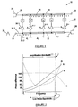
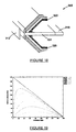
- a distributed low noise amplifier (DLNA) according to the invention is generally designated by the reference numeral 10 in figure 1 .
- the DLNA has an amplification bandwidth 11 (shown in figure 2 ) extending between a first frequency f1 and a second frequency f2.
- the DLNA comprises an input transmission medium (ITM) 12 having a first end 14 and a second end 16.
- the DLNA further comprises an output transmission medium (OTM) 18 having a first end 20 and a second end 22.
- An input of the DLNA is provided at end 14 and an output at end 22.
- Suitable termination means 26 and 28 may be provided at the second end 16 of the ITM 12 and at the first end 20 of the OTM 18.
- the DLNA comprises an amplifier arrangement 30 comprising at least first and second amplifier parts 30.1 to 30.n connected at an input 32 of the arrangement to the input transmission medium and at an output 34 of the arrangement to the output transmission medium, to provide at least first and second paths 36.1 and 36.2 for an input signal 38 from the input 14 of the distributed amplifier to the output 22 of the distributed amplifier.
- Each of the first and second paths 36.1 and 36.2 being associated with a respective change in phase which is different and wherein the difference is larger than 30 degrees for frequencies in a noise suppression band, to cause a phase difference between noise generated by the amplifier arrangement 30 propagating along the first path and second paths and destructive interference of that noise before the output 22 of the distributed amplifier 10, thereby to suppress noise in the noise suppression band 13.
- the respective gains of at least some adjacent amplifier parts decrease, for example linearly, alternatively exponentially, in a direction from the input 14 of the DLNA towards the output 22 thereof, i.e. A1 > A2 > A3. « > An.
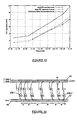
- Figure 2 illustrates various features of a distributed DLNA 10 according to the invention.
- Curve B shows the phase difference between the first amplifier part 30.1 and an intermediate amplifier part.
- Curve A shows the phase difference between the first amplifier part 30.1 and the last amplifier part 30.n.
- Curve C shows the gain profile, which is nearly constant over the amplification bandwidth 11.
- Curve D shows the noise figure of the DLNA 10. It is low within the noise suppression or low noise bandwidth 13. At frequencies lower than the noise suppression bandwidth 11, the phase difference between parts is small. These small differences give only little noise cancellation.
- the phase difference becomes close to 180 degrees, the gain of the amplifier starts to decrease, as the signal from the different parts start to cancel each other. This decreased gain then gives rise to an increase in the noise figure.
- HEMT High Electron Mobility Transistors
- noise generated in the channel of the transistor is coupled capacitively to the gate terminal, but resistively to the drain terminal. This gives an almost 90° phase difference between input noise (at the gate) and output noise (at the drain), so that C r ⁇ C i .
- Almost no noise cancellation then takes place in a conventional distributed amplifier, resulting in a much higher noise figure than in harmonic amplifiers, as referred to in the introduction of this specification.
- Figures 4 and 5 illustrate typical gain and phase profiles respectively against frequency, for parts 30.1 to 30.6 of a DLNA 10 according to the invention.
- a DLNA 10 according to the invention has different time delays from the input 14, through each amplifier part, to the output 22.
- An input signal 38 amplified by the amplifier parts does not arrive at the same time at the output 22, and therefore does not add in phase. This phase difference is referred to as skewing.
- This skewing changes the phase between the aforementioned output noise and aforementioned amplified input noise.
- the correlation between the output noise and amplified input noise can be increased from about 90° to about 180 °, resulting in better noise cancellation.
- the noise figure may be the same as for harmonic amplifiers (proportional to 1 - C im 2 - C re ) (See Table 1).
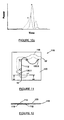
- phase diagrams in figures 7a and 7b show the input noise N i at point 100 in figure 6 and output noise N o at point 102 respectively generated by amplifier part 30.1, compared to an input signal S.
- the input noise is correlated with the output noise, but has a phase difference, which is about 90° in this example.
- Figures 8a and 9a show the time delay from the input 14 to the output 22 through each amplifier part 30.1 to 30.n, for a conventional distributed amplifier and a skewed distributed amplifier 10 according to the invention.
- the resulting amplified input noise is then more than 90° out of phase with the output noise, which results in some noise being cancelled.
- the total noise N 1 compared to the signal arrow in figure 9c is therefore smaller than in the case with no skewing, see figure 8c .
- FIG. 10a shows the dispersion of the output signal compared to the input signal, showing how the skewing has broadened the pulse. If the original pulse shape is required, the output signal may be de-dispersed after the amplifier 10.
- figure 10b illustrates (in the time domain) what happens to the noise of the first amplifier part 30.1 compared to that of a conventional DNLA, which has no skewing.
- Curve A is the output noise
- curve B is the correlated input noise, having a 90° phase shift.
- the amplified input noise will look the same (curve A) when there is no skewing and look like curve C, with skewing.
- the time delay T is normally frequency independent.
- the time delay through an amplifier part 30.1 to 30.n is normally frequency dependent.
- the phase delay difference becomes more, the higher the frequency.
- the result is that the amplifier's gain falls with frequency when the amplifier parts have a frequency independent gain. This can be corrected for by increasing the gain of the amplifier parts for higher frequencies.
- the phase/time delay from the input 12, through an amplifier part 30.1 to 30.n, to the output 22 is the sum of three components namely, a first delay part from the input 12 of the amplifier to an input of the amplifier part, a second delay part through the amplifier part and a third delay part from the output of the amplifier part to the output 22 of the amplifier.
- Skewing can be implemented in a number of ways. It can be implemented by selecting or manipulating the delay through the amplifier parts, or a delay between the amplifier parts on the transmission mediums, or a combination of the two.
- the delay can be implemented by a source inductance and/or some extra time delay circuit.
- the time delay between parts on the input and output transmission medium must be different. This is most easily done by using different dielectric materials, thereby having mediums with different speeds.
- the input and output transmission medium lengths between two parts may also be made different.
- the delay must be larger than d > 125ps for a 90° phase shift at 2GHz. If the transmission speed is half the speed of light, the length l > 19mm to reach this skewing. Note that this is too long to be implemented in an MMIC.
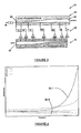
- Figures 11 and 12 show the physical layout of a skewed distributed amplifier 110, which has five amplifier parts 30.1 to 130.5.
- the output transmission medium 118 is a micro-strip transmission medium on FR4 PCB 119, with a ground plane 120 on the one side and the output transmission medium 118 on the other side.
- the relative permittivity of FR4 is about 4, resulting in a transmission medium speed of about half the speed of light.
- the input transmission medium comprises a 0.6mm silver wire 112 suspended in air above the ground plane of the PCB. Because of the gate capacitance of the transistors, the transmission medium speed is a little slower than the speed of light, but still much faster than the output transmission medium speed.
- the transmission medium lengths between amplifier parts are between 5mm and 20mm, which was found to be optimum for minimum noise between 0.5GHz and 2GHz.
- the last part 130.5 has drain-gate feedback to terminate the input transmission medium 112.
- the drains of the transistors are coupled to the output transmission medium through resistors that increase from 15 ⁇ to 250 ⁇ .
- the DC biasing circuit is not shown.
- the sources of the transistors are grounded with a DC-blocking capacitor, having an inductance of about 0.4nH.
- the first amplifier part 30.1 in a DLNA 10 normally comprises a HEMT, with the gate of the HEMT connected to the input transmission medium 12, the source grounded and the drain connected, through other components or a second amplifier stage, to the output transmission medium 18.
- a third noise signal leaves the transistor through the source terminal.
- This source noise current is 180° out of phase with the drain noise current.
- This source noise voltage is amplified (as in a common gate amplifier) and this amplified source noise is added to the drain noise. If the right source impedance is chosen (such as an inductance) the amplified source noise will cancel some of the drain noise.
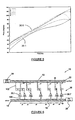
- Figure 13 shows how the minimum noise figure (measured as a noise temperature) of a transistor is reduced by grounding the source through an inductor.
- the inductance on the source may have the disadvantage of making the transistor unstable, normally at frequencies higher that the amplifier's bandwidth. Therefore, a smaller source inductance than optimum may be used.
- the source grounding inductance may also be used in a skewed distributed amplifier in accordance with the invention.
- the combination of the noise cancellation due to the source inductor and skewing gives an even lower noise figure than that of a harmonic amplifier. It was found that the minimum noise figure is achieved when the grounding inductance is increased for each amplifier part in a direction from the input 14 to the output of the amplifier.
- Figure 13 shows the minimum noise figure of a skewed distributed amplifier with increasing source inductance. Because of the decreasing gain of the amplifier parts, the larger inductances do not necessary lead to an instability.
- part of the noise added to the input transmission medium 12 by the amplifier parts 230.1 to 230.7 propagates in the direction of the input 14. This noise is also amplified by the amplifier parts it passes. If the phase delay of the transmission medium between parts is a quarter wavelength, the phase difference between the amplified noise will be more than 180°, which will result in noise cancellation. Therefore, if skewing is implemented by using input and output mediums with different delay times between the parts, such that the difference in delay is comparable to a quarter of a wavelength, it would cause cancellation of backward noise.
- Figures 15 and 16 compare the amplified backward noise generated by the last amplifier part 230.7 for a first distributed amplifier with a small delay on the transmission mediums ( figures 15a and 15b ) and a second distributed amplifier with delays comparable with a quarter of a wavelength on the transmission mediums ( figures 16a and 16b ).
- the input transmission medium 12 is then terminated at first and second ends thereof by a first and second input respectively.
- the input has very little noise and is therefore a good low noise terminator.
- the isolation between the two amplifiers inputs over a broad bandwidth is proportional to the inverse of the number of amplifier parts. Many amplifier parts are therefore required for good isolation.
- Figure 18 shows an example of a continuous amplifier 300, using a continuous dual gate FET, and which the applicant believes would provide a low noise figure.
- a first gate 312 of the FET forms the input transmission medium, with the drain 318 of the FET forming the output transmission medium.
- the decreasing gain may be implemented by tapering the drain line, changing the resistance of the second gate 320 or changing the resistance of the semiconductor 322 between the second gate and drain 318.
- the first amplifier part 30.1 have an output noise i o , which propagate to the output terminal 22, and an input noise, which is amplified by the second part 30.2, giving a noise i i at the output 22.
- the (not skewed) amplified input noise can be divided into three parts: a correlated part that is in-phase with the output noise, a correlated part that is 90-degrees out of phase with the output noise and an uncorrelated part.
- i i i o c r + i a c i + i i,u .
- the noise figure F for a skewing phase ⁇ s is then proportional to N / A, giving F ⁇ s ⁇ ⁇ ⁇ i ⁇ o 2 A 1 ⁇ 1 + c ⁇ cos ⁇ c ⁇ cos ⁇ s - sin ⁇ c ⁇ sin ⁇ s 1 + cos ⁇ s .
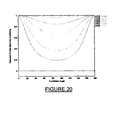
- Figures 19 and 20 show the optimum skewing phase ⁇ s,opt and the corresponding reduction in noise figure between a skewed and not-skewed amplifier F( ⁇ s,opt ) / F(O) for different correlation coefficients.
- the optimum skewing angle is less than about 30°, skewing does not significantly reduce the noise figure.
- the optimum skewing phase is about 90 degrees and it reduces the first amplifier parts noise figure with a factor of 5.
- the optimum skewing reduce the noise figure of the amplifier 10 with a factor of about 1 / 1 - c i 2 ⁇ 2.
- Figure 3 is a diagrammatic illustration of another embodiment of a skewed amplifier 10 according to the invention.
- An impedance of the output transmission medium 18 decreases in a direction from the first end 28 thereof to the output 22 of the amplifier.
- An impedance of the input transmission medium 12 increases in a direction from the first end 14 of the first transmission medium to the second end 16 thereof.
Landscapes
- Engineering & Computer Science (AREA)
- Power Engineering (AREA)
- Amplifiers (AREA)
- Microwave Amplifiers (AREA)
Applications Claiming Priority (2)
| Application Number | Priority Date | Filing Date | Title |
|---|---|---|---|
| ZA200708363 | 2007-10-01 | ||
| PCT/IB2008/053997 WO2009044353A2 (en) | 2007-10-01 | 2008-10-01 | A distributed low noise amplifier |
Publications (2)
| Publication Number | Publication Date |
|---|---|
| EP2193601A2 EP2193601A2 (en) | 2010-06-09 |
| EP2193601B1 true EP2193601B1 (en) | 2016-02-10 |
Family
ID=40263255
Family Applications (1)
| Application Number | Title | Priority Date | Filing Date |
|---|---|---|---|
| EP08835934.4A Not-in-force EP2193601B1 (en) | 2007-10-01 | 2008-10-01 | A distributed low noise amplifier |
Country Status (9)
| Country | Link |
|---|---|
| US (1) | US8344807B2 (enExample) |
| EP (1) | EP2193601B1 (enExample) |
| JP (1) | JP5086439B2 (enExample) |
| KR (1) | KR101484056B1 (enExample) |
| CN (1) | CN101816123B (enExample) |
| AU (1) | AU2008306500B2 (enExample) |
| NZ (1) | NZ584234A (enExample) |
| WO (1) | WO2009044353A2 (enExample) |
| ZA (1) | ZA201001898B (enExample) |
Families Citing this family (11)
| Publication number | Priority date | Publication date | Assignee | Title |
|---|---|---|---|---|
| KR101321185B1 (ko) * | 2012-09-13 | 2013-10-23 | 삼성전기주식회사 | 캐리어 부재 |
| EP2770634B1 (en) * | 2013-02-25 | 2018-09-19 | Telefonaktiebolaget LM Ericsson (publ) | Distributed power amplifier circuit |
| WO2014178261A1 (ja) * | 2013-04-30 | 2014-11-06 | 三菱電機株式会社 | 分布型増幅器 |
| US9825603B2 (en) * | 2015-10-05 | 2017-11-21 | Qorvo Us, Inc. | Active drain terminated distributed amplifier |
| KR20170050397A (ko) * | 2015-10-30 | 2017-05-11 | 전자부품연구원 | 위상 변환기를 이용하여 잡음을 제거하는 저 잡음 증폭기 |
| US10340858B2 (en) | 2016-07-12 | 2019-07-02 | Qorvo Us, Inc. | Linearized distributed amplifier architecture |
| JP2022505108A (ja) * | 2018-10-17 | 2022-01-14 | バヤール イメージング リミテッド | 伝送線路に基づく信号分配および信号集約 |
| CN109450392A (zh) * | 2018-12-27 | 2019-03-08 | 苏州英诺迅科技股份有限公司 | 一种分布式射随放大器 |
| US11498442B2 (en) * | 2019-09-17 | 2022-11-15 | Dr. Ing. H.C. F. Porsche Aktiengesellschaft | Systems and methods for noise cancellation in protective earth resistance check of vehicle onboard battery charger |
| CN113296396B (zh) * | 2021-05-26 | 2022-06-03 | 广东电网有限责任公司 | 一种高频噪声功率增益的自动跟踪系统及方法 |
| CN115360986B (zh) * | 2022-08-30 | 2025-10-28 | 西北大学 | 一种超低功耗超宽带低噪声放大器 |
Family Cites Families (14)
| Publication number | Priority date | Publication date | Assignee | Title |
|---|---|---|---|---|
| US4092616A (en) * | 1976-11-22 | 1978-05-30 | General Dynamics Corporation Electronics Division | Traveling wave power combining apparatus |
| GB8707508D0 (en) * | 1987-03-30 | 1987-09-09 | Era Patents Ltd | Amplifier circuits |
| US5055795A (en) * | 1990-05-29 | 1991-10-08 | At&T Bell Laboratories | Traveling wave type transversal equalizer |
| DE4123437C2 (de) * | 1991-07-16 | 2001-01-04 | Daimler Chrysler Ag | Transistor-Kettenverstärker und Verfahren zur Verbesserung der Rauschzahl |
| US5365197A (en) * | 1993-06-30 | 1994-11-15 | Texas Instruments Incorporated | Low-noise distributed amplifier |
| US6741126B1 (en) * | 1999-09-15 | 2004-05-25 | The North West University | Low noise amplifier arrangement |
| JP3517780B2 (ja) * | 2000-02-22 | 2004-04-12 | 日本電信電話株式会社 | 能動終端回路およびこれを用いた分布増幅器 |
| US6819181B2 (en) * | 2001-12-21 | 2004-11-16 | Motorola, Inc. | Method and structure for integrated circuit interference isolation enhancement |
| US6597243B1 (en) * | 2001-12-31 | 2003-07-22 | Agere Systems, Inc. | Distributed amplifier having a tapered transconductance architecture |
| US6650185B1 (en) | 2002-04-26 | 2003-11-18 | Motorola, Inc | Frequency selective distributed amplifier |
| US7129783B2 (en) * | 2004-10-25 | 2006-10-31 | The Aerospace Corporation | Hybrid active combiner and circulator |
| US7148746B2 (en) * | 2004-10-26 | 2006-12-12 | Andrew Corporation | High efficiency amplifier |
| US7279980B2 (en) * | 2005-04-28 | 2007-10-09 | Regents Of The University Of California | Non-uniform distributed multi-stage circuits |
| JP4792273B2 (ja) * | 2005-10-18 | 2011-10-12 | 株式会社日立国際電気 | 増幅器 |
-
2008
- 2008-10-01 US US12/680,771 patent/US8344807B2/en not_active Expired - Fee Related
- 2008-10-01 EP EP08835934.4A patent/EP2193601B1/en not_active Not-in-force
- 2008-10-01 CN CN200880110012.2A patent/CN101816123B/zh not_active Expired - Fee Related
- 2008-10-01 NZ NZ584234A patent/NZ584234A/xx not_active IP Right Cessation
- 2008-10-01 AU AU2008306500A patent/AU2008306500B2/en not_active Ceased
- 2008-10-01 WO PCT/IB2008/053997 patent/WO2009044353A2/en not_active Ceased
- 2008-10-01 JP JP2010527583A patent/JP5086439B2/ja not_active Expired - Fee Related
- 2008-10-01 KR KR1020107006912A patent/KR101484056B1/ko not_active Expired - Fee Related
-
2010
- 2010-03-17 ZA ZA2010/01898A patent/ZA201001898B/en unknown
Also Published As
| Publication number | Publication date |
|---|---|
| JP2010541450A (ja) | 2010-12-24 |
| CN101816123A (zh) | 2010-08-25 |
| ZA201001898B (en) | 2010-12-29 |
| EP2193601A2 (en) | 2010-06-09 |
| NZ584234A (en) | 2012-12-21 |
| WO2009044353A3 (en) | 2009-05-22 |
| US20100283546A1 (en) | 2010-11-11 |
| WO2009044353A2 (en) | 2009-04-09 |
| AU2008306500A1 (en) | 2009-04-09 |
| CN101816123B (zh) | 2014-08-13 |
| KR101484056B1 (ko) | 2015-01-19 |
| HK1143666A1 (en) | 2011-01-07 |
| AU2008306500B2 (en) | 2012-05-17 |
| US8344807B2 (en) | 2013-01-01 |
| JP5086439B2 (ja) | 2012-11-28 |
| KR20100059927A (ko) | 2010-06-04 |
Similar Documents
| Publication | Publication Date | Title |
|---|---|---|
| EP2193601B1 (en) | A distributed low noise amplifier | |
| US7482874B2 (en) | Non-uniform distributed multi-stage circuits | |
| KR102804379B1 (ko) | 잡음 제거 기능을 갖는 광대역 저잡음 증폭기 | |
| US5046155A (en) | Highly directive, broadband, bidirectional distributed amplifier | |
| US20080055005A1 (en) | Feedback-type variable gain amplifier and method of controlling the same | |
| US7724091B2 (en) | Matrix balun | |
| US7605655B2 (en) | Highly linear differential amplifier with a novel resistive source degeneration network | |
| KR20220002302A (ko) | 잡음 제거 기능을 갖는 저잡음 증폭기 | |
| US7209004B2 (en) | DB-linear variable gain amplifier (VGA) stage with a high broad band | |
| US9356564B1 (en) | Broadband linear amplifier architecture by combining two distributed amplifiers | |
| CN101540593B (zh) | 宽频分配器 | |
| US20090219087A1 (en) | Travelling wave amplifier | |
| HK1143666B (en) | A distributed low noise amplifier | |
| US20250233564A1 (en) | System and method for cross-coupled rc networks for use in differential amplifiers and other circuits | |
| US20190280661A1 (en) | Variable gain amplifier | |
| JPH01208908A (ja) | 可変減衰装置 | |
| US20130249637A1 (en) | Multi-path broadband amplifier |
Legal Events
| Date | Code | Title | Description |
|---|---|---|---|
| PUAI | Public reference made under article 153(3) epc to a published international application that has entered the european phase |
Free format text: ORIGINAL CODE: 0009012 |
|
| 17P | Request for examination filed |
Effective date: 20100322 |
|
| AK | Designated contracting states |
Kind code of ref document: A2 Designated state(s): AT BE BG CH CY CZ DE DK EE ES FI FR GB GR HR HU IE IS IT LI LT LU LV MC MT NL NO PL PT RO SE SI SK TR |
|
| AX | Request for extension of the european patent |
Extension state: AL BA MK RS |
|
| DAX | Request for extension of the european patent (deleted) | ||
| 17Q | First examination report despatched |
Effective date: 20130521 |
|
| GRAP | Despatch of communication of intention to grant a patent |
Free format text: ORIGINAL CODE: EPIDOSNIGR1 |
|
| INTG | Intention to grant announced |
Effective date: 20150818 |
|
| GRAS | Grant fee paid |
Free format text: ORIGINAL CODE: EPIDOSNIGR3 |
|
| GRAA | (expected) grant |
Free format text: ORIGINAL CODE: 0009210 |
|
| AK | Designated contracting states |
Kind code of ref document: B1 Designated state(s): AT BE BG CH CY CZ DE DK EE ES FI FR GB GR HR HU IE IS IT LI LT LU LV MC MT NL NO PL PT RO SE SI SK TR |
|
| REG | Reference to a national code |
Ref country code: GB Ref legal event code: FG4D |
|
| REG | Reference to a national code |
Ref country code: AT Ref legal event code: REF Ref document number: 775077 Country of ref document: AT Kind code of ref document: T Effective date: 20160215 Ref country code: CH Ref legal event code: EP |
|
| REG | Reference to a national code |
Ref country code: IE Ref legal event code: FG4D |
|
| REG | Reference to a national code |
Ref country code: DE Ref legal event code: R096 Ref document number: 602008042311 Country of ref document: DE |
|
| REG | Reference to a national code |
Ref country code: SE Ref legal event code: TRGR |
|
| REG | Reference to a national code |
Ref country code: LT Ref legal event code: MG4D |
|
| REG | Reference to a national code |
Ref country code: NL Ref legal event code: MP Effective date: 20160210 |
|
| REG | Reference to a national code |
Ref country code: AT Ref legal event code: MK05 Ref document number: 775077 Country of ref document: AT Kind code of ref document: T Effective date: 20160210 |
|
| PG25 | Lapsed in a contracting state [announced via postgrant information from national office to epo] |
Ref country code: IT Free format text: LAPSE BECAUSE OF FAILURE TO SUBMIT A TRANSLATION OF THE DESCRIPTION OR TO PAY THE FEE WITHIN THE PRESCRIBED TIME-LIMIT Effective date: 20160210 Ref country code: ES Free format text: LAPSE BECAUSE OF FAILURE TO SUBMIT A TRANSLATION OF THE DESCRIPTION OR TO PAY THE FEE WITHIN THE PRESCRIBED TIME-LIMIT Effective date: 20160210 Ref country code: HR Free format text: LAPSE BECAUSE OF FAILURE TO SUBMIT A TRANSLATION OF THE DESCRIPTION OR TO PAY THE FEE WITHIN THE PRESCRIBED TIME-LIMIT Effective date: 20160210 Ref country code: GR Free format text: LAPSE BECAUSE OF FAILURE TO SUBMIT A TRANSLATION OF THE DESCRIPTION OR TO PAY THE FEE WITHIN THE PRESCRIBED TIME-LIMIT Effective date: 20160511 Ref country code: FI Free format text: LAPSE BECAUSE OF FAILURE TO SUBMIT A TRANSLATION OF THE DESCRIPTION OR TO PAY THE FEE WITHIN THE PRESCRIBED TIME-LIMIT Effective date: 20160210 Ref country code: NO Free format text: LAPSE BECAUSE OF FAILURE TO SUBMIT A TRANSLATION OF THE DESCRIPTION OR TO PAY THE FEE WITHIN THE PRESCRIBED TIME-LIMIT Effective date: 20160510 |
|
| REG | Reference to a national code |
Ref country code: CH Ref legal event code: NV Representative=s name: R.A. EGLI AND CO, PATENTANWAELTE, CH |
|
| PG25 | Lapsed in a contracting state [announced via postgrant information from national office to epo] |
Ref country code: LV Free format text: LAPSE BECAUSE OF FAILURE TO SUBMIT A TRANSLATION OF THE DESCRIPTION OR TO PAY THE FEE WITHIN THE PRESCRIBED TIME-LIMIT Effective date: 20160210 Ref country code: AT Free format text: LAPSE BECAUSE OF FAILURE TO SUBMIT A TRANSLATION OF THE DESCRIPTION OR TO PAY THE FEE WITHIN THE PRESCRIBED TIME-LIMIT Effective date: 20160210 Ref country code: LT Free format text: LAPSE BECAUSE OF FAILURE TO SUBMIT A TRANSLATION OF THE DESCRIPTION OR TO PAY THE FEE WITHIN THE PRESCRIBED TIME-LIMIT Effective date: 20160210 Ref country code: PL Free format text: LAPSE BECAUSE OF FAILURE TO SUBMIT A TRANSLATION OF THE DESCRIPTION OR TO PAY THE FEE WITHIN THE PRESCRIBED TIME-LIMIT Effective date: 20160210 Ref country code: NL Free format text: LAPSE BECAUSE OF FAILURE TO SUBMIT A TRANSLATION OF THE DESCRIPTION OR TO PAY THE FEE WITHIN THE PRESCRIBED TIME-LIMIT Effective date: 20160210 Ref country code: PT Free format text: LAPSE BECAUSE OF FAILURE TO SUBMIT A TRANSLATION OF THE DESCRIPTION OR TO PAY THE FEE WITHIN THE PRESCRIBED TIME-LIMIT Effective date: 20160613 Ref country code: IS Free format text: LAPSE BECAUSE OF FAILURE TO SUBMIT A TRANSLATION OF THE DESCRIPTION OR TO PAY THE FEE WITHIN THE PRESCRIBED TIME-LIMIT Effective date: 20160610 |
|
| REG | Reference to a national code |
Ref country code: FR Ref legal event code: PLFP Year of fee payment: 9 |
|
| PG25 | Lapsed in a contracting state [announced via postgrant information from national office to epo] |
Ref country code: DK Free format text: LAPSE BECAUSE OF FAILURE TO SUBMIT A TRANSLATION OF THE DESCRIPTION OR TO PAY THE FEE WITHIN THE PRESCRIBED TIME-LIMIT Effective date: 20160210 Ref country code: EE Free format text: LAPSE BECAUSE OF FAILURE TO SUBMIT A TRANSLATION OF THE DESCRIPTION OR TO PAY THE FEE WITHIN THE PRESCRIBED TIME-LIMIT Effective date: 20160210 |
|
| REG | Reference to a national code |
Ref country code: DE Ref legal event code: R097 Ref document number: 602008042311 Country of ref document: DE |
|
| PG25 | Lapsed in a contracting state [announced via postgrant information from national office to epo] |
Ref country code: RO Free format text: LAPSE BECAUSE OF FAILURE TO SUBMIT A TRANSLATION OF THE DESCRIPTION OR TO PAY THE FEE WITHIN THE PRESCRIBED TIME-LIMIT Effective date: 20160210 Ref country code: SK Free format text: LAPSE BECAUSE OF FAILURE TO SUBMIT A TRANSLATION OF THE DESCRIPTION OR TO PAY THE FEE WITHIN THE PRESCRIBED TIME-LIMIT Effective date: 20160210 Ref country code: CZ Free format text: LAPSE BECAUSE OF FAILURE TO SUBMIT A TRANSLATION OF THE DESCRIPTION OR TO PAY THE FEE WITHIN THE PRESCRIBED TIME-LIMIT Effective date: 20160210 |
|
| PLBE | No opposition filed within time limit |
Free format text: ORIGINAL CODE: 0009261 |
|
| STAA | Information on the status of an ep patent application or granted ep patent |
Free format text: STATUS: NO OPPOSITION FILED WITHIN TIME LIMIT |
|
| PG25 | Lapsed in a contracting state [announced via postgrant information from national office to epo] |
Ref country code: BE Free format text: LAPSE BECAUSE OF FAILURE TO SUBMIT A TRANSLATION OF THE DESCRIPTION OR TO PAY THE FEE WITHIN THE PRESCRIBED TIME-LIMIT Effective date: 20160210 |
|
| 26N | No opposition filed |
Effective date: 20161111 |
|
| PG25 | Lapsed in a contracting state [announced via postgrant information from national office to epo] |
Ref country code: SI Free format text: LAPSE BECAUSE OF FAILURE TO SUBMIT A TRANSLATION OF THE DESCRIPTION OR TO PAY THE FEE WITHIN THE PRESCRIBED TIME-LIMIT Effective date: 20160210 Ref country code: BG Free format text: LAPSE BECAUSE OF FAILURE TO SUBMIT A TRANSLATION OF THE DESCRIPTION OR TO PAY THE FEE WITHIN THE PRESCRIBED TIME-LIMIT Effective date: 20160510 |
|
| REG | Reference to a national code |
Ref country code: IE Ref legal event code: MM4A |
|
| PG25 | Lapsed in a contracting state [announced via postgrant information from national office to epo] |
Ref country code: LU Free format text: LAPSE BECAUSE OF NON-PAYMENT OF DUE FEES Effective date: 20161001 |
|
| REG | Reference to a national code |
Ref country code: FR Ref legal event code: PLFP Year of fee payment: 10 |
|
| PG25 | Lapsed in a contracting state [announced via postgrant information from national office to epo] |
Ref country code: IE Free format text: LAPSE BECAUSE OF NON-PAYMENT OF DUE FEES Effective date: 20161001 |
|
| PG25 | Lapsed in a contracting state [announced via postgrant information from national office to epo] |
Ref country code: HU Free format text: LAPSE BECAUSE OF FAILURE TO SUBMIT A TRANSLATION OF THE DESCRIPTION OR TO PAY THE FEE WITHIN THE PRESCRIBED TIME-LIMIT; INVALID AB INITIO Effective date: 20081001 Ref country code: CY Free format text: LAPSE BECAUSE OF FAILURE TO SUBMIT A TRANSLATION OF THE DESCRIPTION OR TO PAY THE FEE WITHIN THE PRESCRIBED TIME-LIMIT Effective date: 20160210 |
|
| PG25 | Lapsed in a contracting state [announced via postgrant information from national office to epo] |
Ref country code: MT Free format text: LAPSE BECAUSE OF NON-PAYMENT OF DUE FEES Effective date: 20161031 Ref country code: MC Free format text: LAPSE BECAUSE OF FAILURE TO SUBMIT A TRANSLATION OF THE DESCRIPTION OR TO PAY THE FEE WITHIN THE PRESCRIBED TIME-LIMIT Effective date: 20160210 |
|
| REG | Reference to a national code |
Ref country code: FR Ref legal event code: PLFP Year of fee payment: 11 |
|
| PGFP | Annual fee paid to national office [announced via postgrant information from national office to epo] |
Ref country code: TR Payment date: 20180925 Year of fee payment: 11 |
|
| PGFP | Annual fee paid to national office [announced via postgrant information from national office to epo] |
Ref country code: SE Payment date: 20181019 Year of fee payment: 11 Ref country code: DE Payment date: 20181019 Year of fee payment: 11 |
|
| PGFP | Annual fee paid to national office [announced via postgrant information from national office to epo] |
Ref country code: CH Payment date: 20181019 Year of fee payment: 11 Ref country code: FR Payment date: 20181023 Year of fee payment: 11 Ref country code: GB Payment date: 20181019 Year of fee payment: 11 |
|
| REG | Reference to a national code |
Ref country code: DE Ref legal event code: R119 Ref document number: 602008042311 Country of ref document: DE |
|
| REG | Reference to a national code |
Ref country code: CH Ref legal event code: PL |
|
| PG25 | Lapsed in a contracting state [announced via postgrant information from national office to epo] |
Ref country code: CH Free format text: LAPSE BECAUSE OF NON-PAYMENT OF DUE FEES Effective date: 20191031 Ref country code: LI Free format text: LAPSE BECAUSE OF NON-PAYMENT OF DUE FEES Effective date: 20191031 Ref country code: DE Free format text: LAPSE BECAUSE OF NON-PAYMENT OF DUE FEES Effective date: 20200501 |
|
| PG25 | Lapsed in a contracting state [announced via postgrant information from national office to epo] |
Ref country code: SE Free format text: LAPSE BECAUSE OF NON-PAYMENT OF DUE FEES Effective date: 20191002 |
|
| GBPC | Gb: european patent ceased through non-payment of renewal fee |
Effective date: 20191001 |
|
| PG25 | Lapsed in a contracting state [announced via postgrant information from national office to epo] |
Ref country code: FR Free format text: LAPSE BECAUSE OF NON-PAYMENT OF DUE FEES Effective date: 20191031 Ref country code: GB Free format text: LAPSE BECAUSE OF NON-PAYMENT OF DUE FEES Effective date: 20191001 |
|
| PG25 | Lapsed in a contracting state [announced via postgrant information from national office to epo] |
Ref country code: TR Free format text: LAPSE BECAUSE OF NON-PAYMENT OF DUE FEES Effective date: 20191001 |