EP2193397B1 - Optisches system - Google Patents
Optisches system Download PDFInfo
- Publication number
- EP2193397B1 EP2193397B1 EP05808042.5A EP05808042A EP2193397B1 EP 2193397 B1 EP2193397 B1 EP 2193397B1 EP 05808042 A EP05808042 A EP 05808042A EP 2193397 B1 EP2193397 B1 EP 2193397B1
- Authority
- EP
- European Patent Office
- Prior art keywords
- aperture
- sensor
- optical system
- radiation
- optical
- Prior art date
- Legal status (The legal status is an assumption and is not a legal conclusion. Google has not performed a legal analysis and makes no representation as to the accuracy of the status listed.)
- Expired - Lifetime
Links
Images



Classifications
-
- G—PHYSICS
- G02—OPTICS
- G02B—OPTICAL ELEMENTS, SYSTEMS OR APPARATUS
- G02B27/00—Optical systems or apparatus not provided for by any of the groups G02B1/00 - G02B26/00, G02B30/00
- G02B27/10—Beam splitting or combining systems
- G02B27/1006—Beam splitting or combining systems for splitting or combining different wavelengths
-
- H—ELECTRICITY
- H04—ELECTRIC COMMUNICATION TECHNIQUE
- H04N—PICTORIAL COMMUNICATION, e.g. TELEVISION
- H04N23/00—Cameras or camera modules comprising electronic image sensors; Control thereof
- H04N23/50—Constructional details
- H04N23/55—Optical parts specially adapted for electronic image sensors; Mounting thereof
-
- G—PHYSICS
- G02—OPTICS
- G02B—OPTICAL ELEMENTS, SYSTEMS OR APPARATUS
- G02B27/00—Optical systems or apparatus not provided for by any of the groups G02B1/00 - G02B26/00, G02B30/00
- G02B27/10—Beam splitting or combining systems
- G02B27/1066—Beam splitting or combining systems for enhancing image performance, like resolution, pixel numbers, dual magnifications or dynamic range, by tiling, slicing or overlapping fields of view
-
- G—PHYSICS
- G02—OPTICS
- G02B—OPTICAL ELEMENTS, SYSTEMS OR APPARATUS
- G02B27/00—Optical systems or apparatus not provided for by any of the groups G02B1/00 - G02B26/00, G02B30/00
- G02B27/10—Beam splitting or combining systems
- G02B27/14—Beam splitting or combining systems operating by reflection only
- G02B27/141—Beam splitting or combining systems operating by reflection only using dichroic mirrors
-
- G—PHYSICS
- G02—OPTICS
- G02B—OPTICAL ELEMENTS, SYSTEMS OR APPARATUS
- G02B27/00—Optical systems or apparatus not provided for by any of the groups G02B1/00 - G02B26/00, G02B30/00
- G02B27/10—Beam splitting or combining systems
- G02B27/14—Beam splitting or combining systems operating by reflection only
- G02B27/144—Beam splitting or combining systems operating by reflection only using partially transparent surfaces without spectral selectivity
-
- H—ELECTRICITY
- H04—ELECTRIC COMMUNICATION TECHNIQUE
- H04N—PICTORIAL COMMUNICATION, e.g. TELEVISION
- H04N23/00—Cameras or camera modules comprising electronic image sensors; Control thereof
- H04N23/20—Cameras or camera modules comprising electronic image sensors; Control thereof for generating image signals from infrared radiation only
-
- H—ELECTRICITY
- H04—ELECTRIC COMMUNICATION TECHNIQUE
- H04N—PICTORIAL COMMUNICATION, e.g. TELEVISION
- H04N7/00—Television systems
- H04N7/14—Systems for two-way working
- H04N7/141—Systems for two-way working between two video terminals, e.g. videophone
- H04N7/142—Constructional details of the terminal equipment, e.g. arrangements of the camera and the display
Definitions
- the invention relates to an optical system for detecting radiation.
- Mobile communication devices such as mobile phones, are increasingly becoming multifunction devices. So they not only make phone calls, data transfers, games and playing music, but also increasingly the recording of images by built-in digital color cameras.
- the disadvantage of providing many functions is the space required for the individual function, in particular in combination with the requirement for mechanical stability, which runs counter to the miniaturization of, in particular, mobile communication devices.
- An example of this is the use of large display units (displays) for a display adapted to multimedia services or for controlling a camera built into the communication device, whose lens, control and storage device also requires space.
- the patent application WO 1996/035977 relates to an opening and closing device of an infrared filter for cameras, the device being designed so that the amount of infrared ray passing through a lens barrel to reach photographic elements (11) is adjustable.
- the patent US5070407 relates to a video camera using a silicon diode tube or a similar solid-state photosensitive member as a photo-scanning apparatus, and having a light control device which detects light in the visual spectrum and, on receiving visual spectral light, a mechanical switching device comprising an IR filter and an optical filter neutral density filter positioned in front of the image sensor. Additionally, different filters can substitute other illumination light frequencies.
- An optical system which has at least two apertures each defining an optical axis and a beam path to a sensor.
- the second aperture has a closure device which serves for its substantially light-tight closure.
- a deflection device which deflects radiation as a function of its wavelength. This deflection takes place in such a way that only radiation from a partial wavelength range of the wavelength range detectable by means of the sensor strikes the sensor.
- the second aperture makes it possible for light to strike the sensor from the entire wavelength range detectable by the sensor. This allows for selective detection of radiation which may be used, for example, in combined day / night vision or normal cameras / night vision cameras.
- the deflection device can be formed by a beam splitter and a filter for filtering out a suppression wavelength range.
- the filter is arranged in particular between the first aperture and the beam splitter.
- the suppression wavelength range is defined in particular by the wavelength range detectable by means of the sensor minus the partial wavelength range.
- the deflection device can also be formed by a dichroic beam splitter. This has the advantage that it is possible to dispense with an additional filter in a corresponding dichroic coating. As a result, a component is saved, which can represent a cost and space advantage.
- the optical axes of both apertures are perpendicular to each other.
- the deflection can be realized with simple means.
- Parallel axes allow easy handling by a user when installing the optical system, for example, in a camera.
- lens systems serve to focus the radiation.
- only one lens system can be used for two apertures, which is arranged in front of the sensor in the beam path of both apertures. This can in turn save components.
- Such an optical system can be installed in particular in a camera. Furthermore, it can be used in a sensor module which also has an interface for transmitting data, for example image information acquired by the sensor.
- FIG. 1 For example, the specific sensitivity of a silicon photodiode to optical radiation or light in the visible and infrared ranges is plotted against the wavelength.
- One or more silicon photodiodes can be used as a photosensitive sensor.
- CCD elements etc. can also be used as sensors.
- the specific sensitivity is plotted in amperes per watt, taking into account the current delivered by the silicon photodiode and the radiant power incident on the silicon photodiode.
- the wavelength is given in nanometers.
- the silicon photodiode is photosensitive in a wavelength range of about 400 nanometers to 1100 nanometers.
- the photosensitivity in a wide range of the infrared range of about 750 nanometers to 1100 nanometers is significantly higher than the photosensitivity in the visible range SB between about 400, which is perceived as a blue hue B and 750 nanometers, which is perceived as a red hue R.
- the photosensitivity steadily increases over the wavelength for silicon until a maximum in the range of about 900 to 1000 nanometers is reached.
- filters are placed in front of the photosensitive sensor for digital color cameras with silicon photodiodes or CCD elements as sensors, which strongly suppresses the infrared spectral component or, ideally, completely absorbed. Without this filter, the color information in the visible region would depend very much on the spectral composition of the ambient light, so that no useful color information can be obtained Normally false pictures would be the rule. Only in the case of a spectral response that corresponds exactly to the parameterization of the module would a reasonably correct color representation be possible.
- an optical system OS is illustrated with a sensor S designed as a silicon photodiode or CCD element.
- the sensor S thus has a photosensitivity in the visible range, and a comparatively higher photosensitivity in the infrared range.
- the sensor S is applied to a printed circuit board LP, which provides the readout and control electronics required for the sensor S.
- the sensor S may be exposed to radiation entering either through the first aperture A1 or the second aperture A2.
- the apertures thus each define a beam path, ie first and second beam path, to the sensor S.
- the apertures are each provided with a cover glass D, which serves to protect the underlying elements.
- a lens system LS which serves to focus the light rays entering through the respective aperture, that is to say first aperture A1 or second aperture A2.
- an infrared cut filter IRF which is arranged between the lens system LS in the first beam path and a beam splitter ST.
- the beam splitter serves to direct the radiation which enters through the first aperture A1 or the second aperture A2 onto the sensor S.
- a beam L1 is split into a visible beam V1 with a contribution to visible light and an infrared beam I1 with the contribution to infrared radiation.
- the infrared beam I1 is blocked by the infrared blocking filter IRF, so that it can not hit the sensor S, where it would deteriorate as an interference signal, the color information in the visible radiation range.
- the visible beam V1 passes through the infrared blocking filter IRF through the beam splitter ST and impinges on the sensor S. Thus, only radiation in the visible wavelength range SB impinges on the sensor S through the first aperture A1.
- the infrared blocking filter IRF for this purpose has a transmission coefficient of near 1 for visible radiation SB, and a transmission coefficient near 0 for the infrared range.
- the deflection device is realized for the wavelength-dependent deflection of light beams through the beam splitter ST and the infrared cut-off filter IRF.
- the situation at the second aperture A2 is illustrated by a second light beam L2, which in turn is shown split into a visible light beam V2 and a second infrared light beam I2. Both the second visible beam V2, as well as the second infrared beam I2 occur freely, are deflected by the beam splitter ST and thus meet the sensor S.
- the second aperture A2 is kept as light-tight as possible by a shutter V, so that only radiation entering through the aperture A1 is detected by the sensor S.
- suitable electronics which is located on the printed circuit board LP, by the suppressed Infrared component qualitatively satisfactory images are generated.
- optical system in a camera
- no second imaging optics, no complex mechanism, and no second sensor is required.
- the required in FIG. 2 illustrated embodiment no moving optical components for pivoting an infrared blocking filter IRF.
- Movable optical components would require precise and robust mechanics, since the positioning of the filter would have to be reliable in a variety of environmental conditions, such that when operating as a normal color camera, that is, when operating in daylight, no infrared radiation passes the infrared blocking filter IRF Sensor S, so for example silicon photodiodes meet.
- the mechanism would have to be designed so that it is correspondingly stable, so that the installation of the optical system in a mobile phone as a communication device standard falls of 1.5 meters on a stone floor without damage are overcome.
- Such a precise and stable mechanism would be, apart from the implementation effort, the especially in miniaturized mobile devices, such as cameras in mobile phones, is difficult to lead to high costs.
- the opening of the shutter V can be done manually by the user of a communication device in which the optical system is installed. Alternatively or additionally, an automatic control depending on the ambient brightness may be provided.
- an active light source can be switched, which ensures absolute functionality in absolute darkness -also also missing IR radiation- a good functionality. This can e.g. by an infrared LED as it is used in remote controls or IRDA transmitting and / or receiving units or transceivers, are realized.
- FIG. 2 are the first optical axis OA1, which is defined by the first aperture A1, and the second optical axis OA2, which is defined by the second aperture A2, perpendicular to each other.
- the communication device is also rotated by 90 ° when operating in daylight or darkness.
- FIG. 3 a further embodiment is shown in which the deflection device is realized by means of a dichroic beam splitter.
- the deflection device is realized by means of a dichroic beam splitter.
- first optical axis OA1 and second optical axis OA2 perpendicular to each other.
- the dichroic beam splitter DST is used for the wavelength-dependent deflection of radiation. This is again explained on the basis of selected light beams.
- the light beam L1 ' is again shown split in a visible beam V1 'and an infrared beam I1' in order to explain the paths of the respective beams.
- the visible beam V1 ' passes through the dichroic beam splitter DST and impinges on the sensor S.
- Paid dichroic beam splitters DST is thus distinguished by the fact that radiation in the visible wavelength range has a very high transmission coefficient through the dichroic beam splitter DST, which is close to 1.
- the situation is different for radiation in the infrared range.
- the infrared beam I1 also enters through the first aperture A1.
- the in FIG. 3 The dichroic beam splitters shown thus continue to be distinguished by the fact that radiation in the infrared range has a very high reflection coefficient, which is close to 1. By negligible absorption in the dichroic beam splitter DST can be ensured that no unwanted losses occur.
- the particular infrared absorbing layer may be formed for example by black velvet or matt black paint.
- the embodiment shown since this function is adopted by a corresponding dichroic coating of a beam splitter, whereby a dichroic beam splitter DST is formed, the embodiment shown has the advantage that no separate infrared blocking filter IRF is required. This can save a component, reducing space requirements and possibly reducing costs.
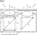
- FIG. 4 a further embodiment is shown in which the first optical axis OA1 of the first aperture A1 is arranged parallel to the second optical axis OA2 of the second aperture A2.
- a deflection prism is furthermore provided which directs radiation which enters through the second aperture A2 onto the sensor S via the beam splitter ST.
- FIG. 5 Furthermore, an embodiment is shown in which only one lens system LS is required, in which the lens system LS between the beam splitter ST and sensor S is arranged.
- the lens system LS between the beam splitter ST and sensor S is arranged.
- FIG. 5 shown Embodiment can also be implemented with a conventional beam splitter ST and an infrared cut filter IRF, as well as in FIG. 4 shown embodiment with a dichroic beam splitter and without infrared cut filter IRF, etc.
- the aperture-side lens system (s) can also be integrated into the respective cover glass.
- domed coverslips act as lenses.
- one or more lens systems can be integrated into the beam splitter. This is realized in particular by correspondingly curved surfaces of the beam splitter. This can in turn save components.
- the opening of the shutter V - as already explained - by manual selection of the user can be done manually or automatically, if a predetermined intensity threshold of the ambient radiation is exceeded.
- This threshold value can in turn be determined by a control unit in the camera.
- the installation of an infrared light source is provided.
- the infrared light source for example, by an LED (Light Emitting Diode), the illumination of the field of view of the camera significantly increase in the dark. This makes it possible to illuminate even absolutely dark rooms in the near infrared range well and make them visible on the display with the help of the built-in communication device camera. Turning on and off the infrared light source can in turn be controlled manually or by an automatic.
- An optical system as described can be installed in a camera as already explained. Furthermore, it can find application in a night vision device. Camera or night vision device may in turn be incorporated in a mobile communication device such as a mobile phone, a PDA (Personal Digital Assistant), a portable computer, etc.
- a photosensitivity in the visible range SB and infrared range was considered.
- a corresponding optical sensor By using a corresponding optical sensor, other wavelength ranges can be considered.
Landscapes
- Physics & Mathematics (AREA)
- Engineering & Computer Science (AREA)
- Multimedia (AREA)
- Signal Processing (AREA)
- General Physics & Mathematics (AREA)
- Optics & Photonics (AREA)
- Spectroscopy & Molecular Physics (AREA)
- Blocking Light For Cameras (AREA)
- Studio Devices (AREA)
Description
- Die Erfindung betrifft ein optisches System zum Erfassen von Strahlung.
- Mobile Kommunikationsgeräte, wie beispielsweise Mobiltelefone, entwickeln sich zunehmend zu Multifunktionsgeräten. So ermöglichen sie nicht nur Telefonate, Datenübertragungen, Spiele und das Abspielen von Musik, sondern zunehmend auch die Aufnahme von Bildern durch eingebaute digitale Farbkameras.
- Nachteil an der Bereitstellung vieler Funktionen ist der für die einzelne Funktion benötigte Platz, insbesondere in Kombination mit der Anforderung an mechanische Stabilität, welcher der Miniaturisierung von insbesondere mobilen Kommunikationsgeraten entgegen läuft. Ein Beispiel hierfür ist der Einsatzgroßer Anzeigeeinheiten (Displays) für eine an Multimediadienste angepasste Anzeige oder zur Steuerung einer in das Kommunikationsgerät eingebauten Kamera, deren Objektiv, Steuer- und Speichereinrichtung ebenfalls Platz benötigt.
- Die Patentanmeldung
WO 1996/035977 bezieht sich auf eine Öffnungs- und Schließvorrichtung eines Infrarot-Filters für Kameras, wobei die Vorrichtung so konstruiert ist, dass die Menge des Infrarotstrahls die durch einen Linsenzylinder hindurchtritt um fotografische Elemente (11) zu erreichen, einstellbar ist. - Die Patentschrift
US5070407 bezieht sich auf eine Videokamera, die eine Siliziumdiodenröhre oder ein ähnliches lichtempfindliches Festkörper-Aufnehmerelement als Lichtbildabtastvorrichtung verwendet, und eine Lichtsteuervorrichtung aufweist, die Licht im visuellen Spektrum detektiert und bei Empfang von visuellem Spektrallicht eine mechanische Schaltvorrichtung, die einen IR-Filter und einen optischen oder neutralen Dichtefilter vor dem Bildsensor positioniert. Zusätzlich können verschiedene Filter andere Beleuchtungslichtfrequenzen ersetzen. - Weitere relevante Dokumente sind die Patentschriften
JP10108152 JP2003333392 DE19736675 undJP2008140072 - Es ist also Aufgabe der vorliegenden Erfindung, weitere Funkionalitäten in einem mobilen Kommunikationsgerät bereitzustellen, für die kein oder nur wenig zusätzlicher Platz erforderlich ist.
- Diese Aufgabe wird durch den unabhängigen Anspruch gelöst. Vorteilhafte Ausgestaltungen sind Gegenstand der abhängigen Ansprüche. Es ist ein optisches System vorgesehen, das zumindest zwei Aperturen aufweist, die jeweils eine optische Achse definieren sowie einen Strahlengang zu einem Sensor. Hierbei weist die zweite Apertur eine Verschlusseinrichtung auf, welche zu ihrem im Wesentlichen lichtdichten Verschließen dient.
- Mittels des Sensors kann Strahlung in einem Wellenlängenbereich erfasst werden. Im optischen System ist weiterhin eine Umlenkeinrichtung vorgesehen, welche Strahlung in Abhängigkeit von ihrer Wellenlänge umlenkt. Diese Umlenkung erfolgt derart, dass nur Strahlung aus einem Teilwellenlängenbereich des mittels des Sensors erfassbaren Wellenlängenbereichs auf den Sensor trifft.
- Damit kann bewirkt werden, dass durch die erste Apertur fast ausschließlich Licht in nur einem Teil-Wellenlängenbereich auf den Sensor treffen kann. Durch die zweite Apertur kann Licht aus dem gesamten, vom Sensor erfassbaren Wellenlängenbereich auf den Sensor treffen. Dies ermöglicht eine selektive Erfassung von Strahlung, welche beispielsweise bei kombinierten Tag/Nachtsichtgeräten oder normalen Kameras/ Nachtsichtkameras Anwendung finden kann.
- Die Umlenkeinrichtung kann insbesondere durch einen Strahlteiler und einen Filter zum Herausfiltern eines Unterdrückungswellenlängenbereichs gebildet werden. Der Filter ist insbesondere zwischen erster Apertur und Strahlteiler angeordnet.
- Eine derartige Realisierung ist wegen der verwendbaren Standardkomponenten von Vorteil. Der Unterdrückungswellenlängenbereich ist insbesondere durch den mittels des Sensors erfassbaren Wellenlängenbereich abzüglich des Teil-Wellenlängenbereichs definiert.
- Die Umlenkeinrichtung kann auch durch einen dichroitischen Strahlteiler gebildet werden. Dies hat den Vorteil, dass bei einer entsprechenden dichroitischen Beschichtung auf einen zusätzlichen Filter verzichtet werden kann. Dadurch wird ein Bauteil eingespart, was einen Kosten- und Platzvorteil darstellen kann.
- Insbesondere stehen die optischen Achsen beider Aperturen aufeinander senkrecht. Dadurch lässt sich die Umlenkeinrichtung mit einfachen Mitteln realisieren.
- Parallel zueinander angeordnete Achsen ermöglichen eine einfache Handhabung durch einen Benutzer bei Einbau des optischen Systems beispielsweise in eine Kamera.
- In einer vorteilhaften Ausgestaltung dienen Linsensysteme zu einer Fokussierung der Strahlung. Insbesondere kann für zwei Aperturen nur ein Linsensystem verwendet werden, welches im Strahlengang beider Aperturen vor dem Sensor angeordnet ist. Dadurch lassen sich wiederum Komponenten einsparen.
- Ein derartiges optisches System lässt sich insbesondere in eine Kamera einbauen. Weiterhin kann es in einem Sensormodulverwendet werden, welches noch eine Schnittstelle zum Übertragen von Daten wie beispielsweise mittels des Sensors erfasster Bildinformation aufweist.
- Weitere Vorzüge der Erfindung werden anhand ausgewählter Ausführungsbeispiele dargestellt, welche in den Figuren gezeigt sind.
- Es zeigen:
-
Figur 1 die spezifische Empfindlichkeit einer Silizium-Fotodiode gegenüber der Wellenlänge aufgetragen; -
Figur 2 eine beispielhafte Ausgestaltung einer Kamera, bei der ein Infrarot-Sperrfilter zwischen einem Linsensystem und einem Sensor vorgesehen ist; -
Figur 3 eine Ausgestaltung, bei der ein dichroitischer Strahlteiler zwischen einem Sensor und einem Linsensystem vorgesehen ist, sowie ein Strahlungsabsorbierender Bereich vorhanden ist; -
Figur 4 eine Ausgestaltung, bei der die erste und zweite Lichteintrittsöffnung parallel zueinander angeordnet sind. -
Figur 5 : Ein optisches System mit nur einem Linsensystem. - In
Figur 1 ist die spezifische Empfindlichkeit einer Silizium-Fotodiode auf optische Strahlung beziehungsweise Licht im sichtbaren und Infrarotbereich gegenüber der Wellenlänge aufgetragen. Eine oder mehrere Silizium-Photodioden kann als lichtempfindlicher Sensor eingesetzt werden. - Neben Silizium-Photodioden lassen sich auch CCD-Elemente etc. als Sensoren verwenden.
- Die spezifische Empfindlichkeit ist in Ampere pro Watt aufgetragen, wobei der von der Silizium-Fotodiode abgegebene Strom und die auf die Silizium-Fotodiode auftreffende Strahlungsleistung berücksichtigt wird. Die Wellenlänge ist in Nanometer angegeben. Die Silizium-Fotodiode ist in einem Wellenlängenbereich von etwa 400 Nanometer bis 1100 Nanometer lichtempfindlich. Hierbei ist die Lichtempfindlichkeit in einem großen Bereich des Infrarotbereiches von etwa 750 Nanometer bis 1100 Nanometer deutlich höher als die Lichtempfindlichkeit im sichtbaren Bereich SB zwischen etwa 400, was als blauer Farbton B wahrgenommen wird und 750 Nanometer, was als roter Farbton R wahrgenommen wird.
- Die Lichtempfindlichkeit nimmt über der Wellenlänge für Silizium stetig zu, bis ein Maximum im Bereich von etwa 900 bis 1000 Nanometer erreicht wird.
- Auf Grund der geringeren Lichtempfindlichkeit im sichtbaren Wellenlängenbereich werden für digitale Farbkameras mit Silizium-Photodioden oder CCD-Elementen als Sensoren Filter vor den lichtempfindlichen Sensor gesetzt, welcher den infraroten Spektralanteil stark unterdrückt oder im Idealfall vollkommen absorbiert. Ohne dieses Filter würde die Farbinformation im sichtbaren Bereich sehr stark von der spektralen Zusammensetzung des Umgebungslichtes abhängen, so dass keine brauchbare Farbinformation gewonnen werden kann
Im Normalfall wären falschfarbene Bilder die Regel. Lediglich bei einem Spektralverhalten das exakt dem entspricht bei dem das Modul parametrisiert wurde wäre eine halbwegs korrekte Farbdarstellung möglich. - In
Figur 2 ist ein optisches System OS mit einem als Silizium-Fotodiode oder CCD-Element ausgebildeten Sensor S dargestellt. Der Sensor S weist also eine Lichtempfindlichkeit im sichtbaren Bereich, sowie eine im Vergleich dazu höhere Lichtempfindlichkeit im infraroten Bereich auf. Der Sensor S ist auf einer Leiterplatte LP aufgebracht, welche die für den Sensor S erforderliche Auslese- und Steuerelektronik bereitstellt. Auf den Sensor S kann Strahlung treffen, indem sie entweder durch die erste Apertur A1 oder die zweite Apertur A2 eintritt. Die Aperturen definieren also jeweils einen Strahlengang, also ersten und zweiten Strahlengang, zum Sensor S. - Die Aperturen sind jeweils mit einem Deckglas D versehen, welches zum Schutz der darunter liegenden Elemente dient. Unter dem jeweiligen Deckglas D befindet sich ein Linsensystem LS, welches zur Bündelung der durch die jeweilige Apertur, also erste Apertur A1 oder zweite Apertur A2, eintretenden Lichtstrahlen dient.
- Zum Herausfiltern von Infrarotstrahlung dient ein Infrarot-sperrfilter IRF, welches zwischen dem Linsensystem LS im ersten Strahlengang und einem Strahlteiler ST angeordnet ist. Der Strahlteiler dient dazu, die Strahlung, welche durch die erste Apertur A1 oder die zweite Apertur A2 eintritt, auf den Sensor S zu lenken.
- Dies sei anhand einiger Strahlen erläutert. Zur Verdeutlichung ist ein Strahl L1 in einen sichtbaren Strahl V1 mit einem Beitrag an sichtbarem Licht und einem Infrarotstrahl I1 mit dem Beitrag an infraroter Strahlung aufgespaltet. Der Infrarotstrahl I1 wird durch das Infrarotsperrfilter IRF abgeblockt, so dass er nicht auf den Sensor S treffen kann, wo er als Störsignal, die Farbinformation im Bereich sichtbarer Strahlung verschlechtern würde. Der sichtbare Strahl V1 tritt durch das Infrarotsperrfilter IRF durch den Strahlteiler ST hindurch und trifft auf den Sensor S. Durch die erste Apertur A1 trifft also nur Strahlung im sichtbaren Wellenlängenbereich SB auf den Sensor S.
- Das Infrarotsperrfilter IRF weist hierzu einen Durchlasskoeffizienten von nahe 1 für Strahlung im sichtbaren Bereich SB, und einen Durchlasskoeffizienten nahe 0 für den Infrarotbereich auf.
- In
Figur 2 wird also die Umlenkeinrichtung zum wellenlängenabhängigen Umlenken von Lichtstrahlen durch den Strahlteiler ST und den Infrarot-Sperrfilter IRF realisiert. - Die Situation an der zweiten Apertur A2 sei anhand eines zweiten Lichtstrahls L2 dargestellt, der wiederum in einen sichtbaren Lichtstrahl V2 und einen zweiten Infrarot-Lichtstrahl I2 aufgespaltet dargestellt ist. Sowohl der zweite sichtbare Strahl V2, als auch der zweite Infrarotstrahl I2 treten ungehindert ein, werden durch den Strahlteiler ST umgelenkt und treffen somit auf den Sensor S.
- Bei Tageslicht wird die zweite Apertur A2 durch einen Verschluss V möglichst lichtdicht verschlossen gehalten, so dass nur durch die Apertur A1 eintretende Strahlung durch den Sensor S erfasst wird. Damit können bei Tageslicht durch Auslesen des Sensors S mittels einer geeigneten Elektronik, welche sich auf der Leiterplatt LP befindet, durch den unterdrückten Infrarotanteil qualitativ zufrieden stellende Bilder erzeugt werden.
- Bei Dunkelheit wird nun der Verschluss V geöffnet. Damit tritt durch die erste Apertur A1 sichtbare Strahlung ein, durch die zweite Apertur A2 sichtbare Strahlung und Infrarotstrahlung. Da bei Dunkelheit der Anteil sichtbarer Strahlung von A1 und A2 sehr gering ist, trifft im Wesentlichen Infrarot-Strahlung von A2 auf den Sensor S, wodurch auch bei Dunkelheit Infrarot-Abbildungen der Umgebung erzeugt werden können. Daher ist auch ein Verschluß der A1 Apertur nicht zwingend notwendig.
- Bei der Verwendung des in
Figur 2 gezeigten optischen Systems in einer Kamera, lässt sich somit mit einfachen Mitteln eine Nachtsichtkamera herstellen. Dazu ist insbesondere keine zweite Abbildungsoptik, keine komplexe Mechanik, sowie kein zweiter Sensor erforderlich. Dies stellt geringe Produktionskosten sicher. Weiterhin benötigt die inFigur 2 dargestellte Ausführung keine beweglichen optischen Komponenten zum Ein- und Ausschwenken eines Infrarotsperrfilters IRF. Bewegliche optische Komponenten würden eine präzise und robuste Mechanik erfordern, da die Positionierung des Filters unter unterschiedlichsten Umgebungsbedingungen zuverlässig sein müsste, dass im Betrieb als normale Farbkamera, das heißt, bei der Funktionsweise bei Tageslicht, keine infrarote Strahlung an dem Infrarotsperrfilter IRF vorbei, auf den Sensor S, also beispielsweise Silizium-Fotodioden, treffen kann. Dies ist insbesondere dadurch auch aufwendig, da das ganze Kameramodul hermetisch dicht sein muss, um eine Degradation der Kamerafunktion durch Eindringen von Staub oder Feuchtigkeit zu vermeiden. Weiterhin müsste die Mechanik auch dahingehend ausgelegt sein, dass sie entsprechend stabil ist, so dass beim Einbau des optischen Systems in ein Mobiltelefon als Kommunikationsgerät Normstürze von 1,5 Meter auf einen Steinfußboden ohne Schaden überstanden werden. Eine derartige präzise und stabile Mechanik wäre, abgesehen vom Realisationsaufwand, der insbesondere in miniaturisierten mobilen Geräten, wie etwa Kameras in Mobiltelefonen, schwer möglich ist, zu hohen Kosten führen. - Das Öffnen des Verschlusses V kann manuell durch den Benutzer eines Kommunikationsgeräts erfolgen, in das das optische System eingebaut ist. Alternativ oder zusätzlich kann eine automatische Steuerung in Abhängigkeit von der Umgebungshelligkeit vorgesehen sein.
- Auch kann mit dem Verschluß gekoppelt eine aktive Lichtquelle geschaltet werden, die bei absoluter Dunkelheit -also auch fehlender IR Strahlung- eine gute Funktionalität sicherstellt. Dies kann z.B. durch eine Infarot LED wie sie in Fernsteuerungen oder IRDA Sende oder/und Empfangseinheiten bzw. Transceivern Verwendung findet, realisiert werden.
- In
Figur 2 sind die erste optische Achse OA1, welche durch die erste Apertur A1 definiert wird, und die zweite optische Achse OA2, welche durch die zweite Apertur A2 definiert wird, senkrecht zueinander. Bei der Verwendung des optischen Systems inFigur 2 in einer Kamera, welche insbesondere in ein mobiles Kommunikationsgerät eingebaut ist, wird deshalb das Kommunikationsgerät beim Betrieb bei Tageslicht oder Dunkelheit ebenfalls um 90° gedreht. - In
Figur 3 ist eine weitere Ausführungsform gezeigt, bei der die Umlenkeinrichtung mittels eines dichroitischen Strahlteilers realisiert wird. Gleiche Bezugszeichen verweisen auf gleiche Objekte. - Auch in
Figur 3 stehen erste optische Achse OA1 und zweite optische Achse OA2 senkrecht aufeinander. - Der dichroitische Strahlteiler DST dient zur wellenlängenabhängigen Ablenkung von Strahlung. Dies sei wiederum anhand ausgewählter Lichtstrahlen erläutert. Der Lichtstrahl L1' ist wiederum in einem sichtbaren Strahl V1' und einen Infrarotstrahl I1' aufgespaltet dargestellt, um die Wege der jeweiligen Strahlen zu erläutern. Der sichtbare Strahl V1' tritt durch den dichroitischen Strahlteiler DST hindurch und trifft auf den Sensor S.
- Der in
Figur 3 gezahlte dichroitische Strahlteiler DST zeichnet sich also dadurch aus, dass Strahlung im sichtbaren Wellenlängenbereich einen sehr hohen Transmissionskoeffizienten durch den dichroitischen Strahlteiler DST, welcher in der Nähe von 1 liegt, aufweist. Die Situation ist anders für Strahlung im infraroten Bereich. Der Infrarotstrahl I1' tritt ebenfalls durch die erste Apertur A1 ein. Auf dem Weg durch den dichroitischen Strahlteiler DST wird er an dessen Grenzfläche GS reflektiert. Der inFigur 3 gezeigte dichroitische Strahlteiler zeichnet sich also weiterhin dadurch aus, dass Strahlung im infraroten Bereich einen sehr hohen Reflexionskoeffizienten, welcher nahe bei 1 liegt, aufweist. Durch eine zu vernachlässigende Absorption im dichroitischen Strahlteiler DST kann sichergestellt werden, dass keine ungewünschten Verluste auftreten. - Der abgelenkte Infrarotstrahl I1' trifft auf eine strahlungsabsorbierende Schicht IRS. Diese dient dazu, dass sich keine Streustrahlung im in
Figur 3 gezeigten optischen System befindet. Die insbesondere Infrarot absorbierende Schichte kann beispielsweise durch schwarzen Samt oder mattschwarze Lackierung gebildet sein. - Somit weist die in
Figur 3 gezeigte Ausführung den Vorteil auf, dass kein separates Infrarot-Sperrfilter IRF, wie in Figur 2 benötigt wird, da diese Funktion durch eine entsprechende dichroitische Beschichtung eines Strahlteilers, wodurch ein dichroitischer Strahlteiler DST gebildet wird, übernommen wird. Dadurch lässt sich eine Komponente einsparen, wodurch der Platzbedarf verringert wird und eventuell auch Kosten verringert werden können. - In
Figur 4 ist eine weitere Ausführungsform dargestellt, bei der die erste optische Achse OA1 der ersten Apertur A1 parallel zur zweiten optischen Achse OA2 der zweiten Apertur A2 angeordnet ist. - Durch die parallele Anordnung von erster optischer Achse OA1 und zweiter optischer Achse OA2 kann das Drehen eines Kommunikationsgeräts, in dem eine Kamera mit einem in
Figur 4 gezeigten optischen System eingebaut ist, vermieden werden, da eben die optischen Achsen gleich ausgerichtet sind. Dies erhöht die Benutzerfreundlichkeit beim Einbau des optischen Systems in ein Kommunikationsgerät. - Um diese gleiche Ausrichtung zu ermöglichen, ist in der in
Figur 4 gezeigten Ausgestaltung weiterhin ein Umlenkprisma vorgesehen, welches Strahlung, die durch die zweite Apertur A2 eintritt, über den Strahlteiler ST auf den Sensor S lenkt. - In
Figur 5 ist weiterhin eine Ausführungsform dargestellt, bei der nur ein Linsensystem LS erforderlich ist, in dem das Linsensystem LS zwischen Strahlteiler ST und Sensor S angeordnet ist. Durch eine entsprechende Bemessung der Größe des dichroitischen Strahlteilers DST und der Größe der ersten Apertur A1 und der zweiten Apertur A2, sowie dem Abstand zwischen dem Deckglas D und dem dichroitischen Strahlteiler DST, kann auf ein zusätzliches, focussierendes Linsensystem LS zwischen Deckglas D und dichroitischen Strahlteiler DST verzichtet werden. - Die Verwendung nur eines Linsensystems führt durch die Einsparung einer Komponente zu geringeren Kosten und einem geringeren Platzbedarf.
- Die Merkmale der in den einzelnen Figuren dargestellten Ausführungsformen können selbstverständlich miteinander kombiniert werden, so dass zum Beispiel die in
Figur 5 gezeigte Ausführungsform auch mit einem herkömmlichen Strahlteiler ST und einem Infrarot-Sperrfilter IRF umgesetzt werden kann, ebenso wie die inFigur 4 gezeigte Ausführungsform mit einem dichroitischen Strahlteiler und ohne Infrarot-Sperrfilter IRF, etc. - Weiterhin ist es auch vorgesehen, ein Linsensystem sowohl a-perturseitig, wie in
Fig. 3 dargestellt als auch sensorseitig, wie inFig. 5 dargestellt vorzusehen. Dies hat den Vorteil, durch entsprechend kleinere Linsensystem den Platz optimal auszunutzen oder auch eine sehr gut anpassbare Fokussierung zu realisieren. Das oder die aperturseitigen Linsensysteme lassen sich auch in das jeweilige Deckglas integrieren. Insbesondere fungieren gewölbte Deckgläser als Linsen. - Weiterhin kann ein oder mehrere Linsensysteme in den Strahlteiler integriert werden.
Dies wird insbesondere durch entsprechend gewölbte Oberflächen des Strahlteilers realisiert. Damit lassen sich wiederum Bauteile einsparen. - Bei Verwendung eines optischen Systems gemäß einer der Ausführungsformen in einer Kamera, kann das Öffnen des Verschlusses V - wie bereits dargelegt - durch bewusste Auswahl des Benutzers manuell erfolgen oder automatisch, falls ein festgelegter Intensitätsschwellwert der Umgebungsstrahlung unterschritten wird. Dieser Schwellwert kann wiederum durch eine Kontrolleinheit in der Kamera festgelegt werden.
- Weiterhin ist bei der Verwendung in einer Kamera der Einbau einer infraroten Lichtquelle vorgesehen. Die infrarote Lichtquelle kann beispielsweise durch eine LED (Light Emitting Diode) die Ausleuchtung des Blickfeldes der Kamera bei Dunkelheit deutlich steigern. Dadurch ist es möglich, sogar absolut dunkle Räume im nahen Infrarotbereich gut auszuleuchten und mit Hilfe der im Kommunikationsgerät eingebauten Kamera auf dem Display sichtbar zu machen. Das Ein- und Ausschalten der infraroten Lichtquelle kann wiederum manuell oder von einer Automatik gesteuert werden.
- Ein optisches System wie beschrieben lässt sich, wie bereits dargelegt, in eine Kamera einbauen. Weiterhin kann es Anwendung in einem Nachtsichtgerät finden. Kamera oder Nachtsichtgerät können wiederum in einem mobilen Kommunikationsgerät, wie etwa einem Mobiltelefon, einem PDA (Personal Digital Assistent), einem tragbaren Computer etc., eingebaut sein.
Im Rahmen der Beispiele wurde eine Lichtempfindlichkeit im sichtbaren Bereich SB und Infrarotbereich betrachtet. Durch die Verwendung eines entsprechenden optischen Sensors lassen sich auch andere Wellenlängenbereiche betrachten. -
- A1
- erste Apertur
- A2
- zweite Apertur
- OA1
- erste optische Achse
- OA2
- zweite optische Achse
- D
- Deckglas
- GS
- Grenzfläche
- DST
- dichroitischer Strahlteiler
- IRS
- Infrarot absorbierende Schicht
- LF
- Linsensystem
- S
- Sensor
- LP
- Leiterplatte
- V1,V1',V2
- sichtbare Lichtstrahlen
- I1,I1',I2
- Infrarot-Lichtstrahlen
- ST
- Strahlteiler
- IRS
- Infrarot-Sperrfilter
- GF
- Grenzfläche
Claims (11)
- Optisches System (OS) zum Erfassen von Strahlung aus einem selektierbaren Teil-Wellenlängenbereich mita. einem Sensor (S) zum Detektieren von Strahlung in einem Wellenlängenbereich, in welchem der Teil- Wellenlängenbereich enthalten ist;b. einer ersten Apertur (A1), welche einen ersten Strahlengang zu dem Sensor (S) sowie eine erste optische Achse (OA1) definiert;c. und einer zweiten Apertur (A2), welche einen zweiten Strahlengang zu dem Sensor (S) sowie eine zweite optische Achse (OA2) definiert;d. einer Umlenkeinrichtung (IRF, ST, DST) zum in Abhängigkeit von der Wellenlänge selektiven Umlenken von durch die erste Apertur (A1) eintretender Strahlung, wobei die Umlenkeinrichtung (IRF, ST, DST) durch einen dichroitischen Strahlteiler (DST) gebildet ist und nur Strahlung aus dem Teil- Wellenlängenbereich auf den Sensor treffen lässt;e. einer Verschlusseinrichtung (V) zum lichtdichten Verschließen der zweiten Apertur (A2) derart, dass entweder nur durch die erste Apertur (A1) oder durch die ersten und zweiten Aperturen (A1, A2) eintretende Strahlung auf den Sensor trifft.
- Optisches System (OS) nach Anspruch 1, bei dem die Umlenkeinrichtung (IRF, ST, DST) durch einen Strahlteiler (ST) und einen Filter (IRF) zum Herausfiltern von Strahlung eines Unterdrückungswellenlängebereichs gebildet ist.
- Optisches System (OS) nach Anspruch 1 oder 2, bei dem weiterhin ein Absorptionselement (IRS) zum Absorbieren von nicht auf den Sensor treffender, durch die Aperturen (A1, A2) eingetretener Strahlung vorgesehen ist.
- Optisches System (OS) nach einem der vorhergehenden Ansprüche, bei dem die erste Apertur (A1) eine erste optische Achse (OA1) festlegt und die zweite Apertur (A2) eine zweite optische Achse (OA2) und die optischen Achsen (OA1, OA2) aufeinander senkrecht stehen.
- Optisches System (OS) nach einem der vorhergehenden Ansprüche 1 bis 3, bei dem die erste Apertur (A1) eine erste optische Achse (OA1) festlegt und die zweite Apertur (A2) eine zweite optische Achse (OA2) bei dem die optischen Achsen (OA1, OA2) parallel zueinander sind und ein weiteres Umlenkelement (UP) vorgesehen ist.
- Optisches System (OS) nach einem der vorhergehenden Ansprüche, bei dem für erste Apertur (A1) und zweite Apertur (A2) jeweils ein Linsensystem (LS) vorgesehen ist.
- Optisches System (OS) nach einem der vorhergehenden Ansprüche 1 bis 5, bei dem ein Linsensystem (LS) zwischen Umlenkeinrichtung (DST, ST, IRF) und Sensor (S) vorgesehen ist, durch welches durch die erste Apertur (A1) eintretende Strahlung und durch die zweite Apertur (A2) eintretende Strahlung hindurchtritt.
- Kamera mit einem optischen System gemäß einem der Ansprüche 1 bis 7 und weiterhin einer Speichereinheit zum Abspeichern der von Sensor erfassten Strahlungsinformation, einer Steuereinrichtung zum Steuern des Auslesens des Sensors (S) und der Verschlusseinrichtung (V) .
- Sensormodul mit einem optischen System gemäß einem der Ansprüche 1 bis 7 und einer Schnittstelle zur Weiterleitung von mittels des optischen Systems erfasster Bildinformation an externe Speicher- und Steuerungskomponenten.
- Mobiles Gerät, mit einem optischen System gemäß einem der Ansprüche 1 bis 7 oder einer Kamera gemäß Anspruch 8 oder einem Sensormodul gemäß Anspruch 9.
- Mobiles Gerät nach Anspruch 10, wobei das mobile Gerät ein Mobiltelefon ist.
Applications Claiming Priority (2)
| Application Number | Priority Date | Filing Date | Title |
|---|---|---|---|
| DE102004060616A DE102004060616A1 (de) | 2004-12-16 | 2004-12-16 | Optisches System |
| PCT/EP2005/055961 WO2006063910A1 (de) | 2004-12-16 | 2005-11-14 | Optisches system |
Publications (2)
| Publication Number | Publication Date |
|---|---|
| EP2193397A1 EP2193397A1 (de) | 2010-06-09 |
| EP2193397B1 true EP2193397B1 (de) | 2018-12-26 |
Family
ID=35622048
Family Applications (1)
| Application Number | Title | Priority Date | Filing Date |
|---|---|---|---|
| EP05808042.5A Expired - Lifetime EP2193397B1 (de) | 2004-12-16 | 2005-11-14 | Optisches system |
Country Status (3)
| Country | Link |
|---|---|
| EP (1) | EP2193397B1 (de) |
| DE (1) | DE102004060616A1 (de) |
| WO (1) | WO2006063910A1 (de) |
Families Citing this family (1)
| Publication number | Priority date | Publication date | Assignee | Title |
|---|---|---|---|---|
| CN107241467B (zh) * | 2017-05-11 | 2020-08-07 | Oppo广东移动通信有限公司 | 电子装置 |
Citations (2)
| Publication number | Priority date | Publication date | Assignee | Title |
|---|---|---|---|---|
| US5070407A (en) * | 1990-05-11 | 1991-12-03 | Wheeler Ernest E | Filter changing mechanism for a video camera |
| WO1996035977A1 (en) * | 1995-05-10 | 1996-11-14 | Korea Communications Co., Ltd. | An opening and shutting device of infrared-ray filter for cameras |
Family Cites Families (9)
| Publication number | Priority date | Publication date | Assignee | Title |
|---|---|---|---|---|
| US5161051A (en) * | 1990-12-13 | 1992-11-03 | Hughes Aircraft Company | Simultaneous dual field of view sensor |
| JP3337573B2 (ja) * | 1994-11-08 | 2002-10-21 | オリンパス光学工業株式会社 | 情報通信用端末装置 |
| GB9507671D0 (en) * | 1995-04-13 | 1995-11-08 | Barr & Stroud Ltd | Dual waveband optical system |
| JPH10108152A (ja) | 1996-09-27 | 1998-04-24 | Sanyo Electric Co Ltd | 携帯情報端末 |
| DE19736675A1 (de) | 1997-08-22 | 1999-02-25 | Siemens Ag | Mobiles Bildtelefon |
| US8049816B2 (en) * | 2001-11-16 | 2011-11-01 | Nokia Corporation | Mobile terminal device having camera system |
| JP4040358B2 (ja) * | 2002-03-15 | 2008-01-30 | シャープ株式会社 | 撮影機能を有した携帯電話機 |
| JP2003333392A (ja) | 2002-05-14 | 2003-11-21 | Fuji Photo Film Co Ltd | 撮像機能付情報通信端末装置 |
| JP2008140072A (ja) | 2006-11-30 | 2008-06-19 | Toshiba Tec Corp | 電子機器 |
-
2004
- 2004-12-16 DE DE102004060616A patent/DE102004060616A1/de not_active Withdrawn
-
2005
- 2005-11-14 WO PCT/EP2005/055961 patent/WO2006063910A1/de not_active Ceased
- 2005-11-14 EP EP05808042.5A patent/EP2193397B1/de not_active Expired - Lifetime
Patent Citations (2)
| Publication number | Priority date | Publication date | Assignee | Title |
|---|---|---|---|---|
| US5070407A (en) * | 1990-05-11 | 1991-12-03 | Wheeler Ernest E | Filter changing mechanism for a video camera |
| WO1996035977A1 (en) * | 1995-05-10 | 1996-11-14 | Korea Communications Co., Ltd. | An opening and shutting device of infrared-ray filter for cameras |
Also Published As
| Publication number | Publication date |
|---|---|
| DE102004060616A1 (de) | 2006-07-06 |
| EP2193397A1 (de) | 2010-06-09 |
| WO2006063910A1 (de) | 2006-06-22 |
Similar Documents
| Publication | Publication Date | Title |
|---|---|---|
| DE102010061512B4 (de) | Bilderfassungsvorrichtung, Verfahren zum Erfassen von Bildern unter Verwendung von Infrarotlicht oder sichtbarem Licht und computerlesbares Medium | |
| DE69132022T2 (de) | Fotografiervorrichtung | |
| DE60215909T2 (de) | Vorrichtung zur Flammenerkennung | |
| EP0362737A1 (de) | Gerät und Verfahren für das Umwandeln von Bildern oder Abbildern in Videosignale | |
| US20230358926A1 (en) | Optical image lens assembly, imaging apparatus and electronic device | |
| US9936143B2 (en) | Imager module with electronic shutter | |
| DE3710199C2 (de) | Automatische Fokussiereinrichtung für Kameras | |
| DE19614746A1 (de) | Doppel-Wellenband-Optiksystem | |
| DE10028233A1 (de) | Farbkameraanordnung mit einem photosensitiven,Iv ladungsgekoppelten Bildwandler (CCD) | |
| DE2752929A1 (de) | Fotografische kamera mit einer belichtungssteuerschaltung und mit einer fokussiervorrichtung | |
| CH689703A5 (de) | Photomikroskop. | |
| DE3721557C2 (de) | Photographische Einwegkamera | |
| EP1160549A2 (de) | Beleuchtungssensor mit optischer Begrenzung des Sonnenlichts | |
| JPS61109036A (ja) | テレビレンズの表示装置 | |
| WO2006063910A1 (de) | Optisches system | |
| DE2625011C3 (de) | Photographische Kamera | |
| WO2008000443A1 (de) | Abbilden optischer bilder auf einen bildsensor mittels einer faseroptischen platte bzw. eines faserkeils | |
| US4314747A (en) | Light shielding device for automatic focus detecting | |
| EP2008447B1 (de) | Suchersystem für eine kamera | |
| EP1207687A1 (de) | Bildaufnahmevorrichtung | |
| WO2020225109A1 (de) | Erfassungsvorrichtung mit einer bilderfassungseinrichtung und einem trägermedium sowie erfassungssystem mit einer derartigen erfassungsvorrichtung und einem gerät mit einem bildschirm | |
| US10158791B2 (en) | Camera device with red halo reduction | |
| DE3324223A1 (de) | Leuchtsucher | |
| DE4235406C1 (de) | Falschfarbenkamera | |
| DE3113507C2 (de) |
Legal Events
| Date | Code | Title | Description |
|---|---|---|---|
| PUAI | Public reference made under article 153(3) epc to a published international application that has entered the european phase |
Free format text: ORIGINAL CODE: 0009012 |
|
| 17P | Request for examination filed |
Effective date: 20090803 |
|
| AK | Designated contracting states |
Kind code of ref document: A1 Designated state(s): AT BE BG CH CY CZ DE DK EE ES FI FR GB GR HU IE IS IT LI LT LU LV MC NL PL PT RO SE SI SK TR |
|
| AX | Request for extension of the european patent |
Extension state: AL BA HR MK YU |
|
| RAP1 | Party data changed (applicant data changed or rights of an application transferred) |
Owner name: HEWLETT-PACKARD DEVELOPMENT COMPANY, L.P. |
|
| DAX | Request for extension of the european patent (deleted) | ||
| RAP1 | Party data changed (applicant data changed or rights of an application transferred) |
Owner name: QUALCOMM INCORPORATED |
|
| 17Q | First examination report despatched |
Effective date: 20141023 |
|
| STAA | Information on the status of an ep patent application or granted ep patent |
Free format text: STATUS: EXAMINATION IS IN PROGRESS |
|
| GRAP | Despatch of communication of intention to grant a patent |
Free format text: ORIGINAL CODE: EPIDOSNIGR1 |
|
| STAA | Information on the status of an ep patent application or granted ep patent |
Free format text: STATUS: GRANT OF PATENT IS INTENDED |
|
| INTG | Intention to grant announced |
Effective date: 20180705 |
|
| GRAS | Grant fee paid |
Free format text: ORIGINAL CODE: EPIDOSNIGR3 |
|
| GRAA | (expected) grant |
Free format text: ORIGINAL CODE: 0009210 |
|
| STAA | Information on the status of an ep patent application or granted ep patent |
Free format text: STATUS: THE PATENT HAS BEEN GRANTED |
|
| AK | Designated contracting states |
Kind code of ref document: B1 Designated state(s): AT BE BG CH CY CZ DE DK EE ES FI FR GB GR HU IE IS IT LI LT LU LV MC NL PL PT RO SE SI SK TR |
|
| REG | Reference to a national code |
Ref country code: GB Ref legal event code: FG4D Free format text: NOT ENGLISH |
|
| REG | Reference to a national code |
Ref country code: CH Ref legal event code: EP |
|
| REG | Reference to a national code |
Ref country code: DE Ref legal event code: R096 Ref document number: 502005015972 Country of ref document: DE |
|
| REG | Reference to a national code |
Ref country code: AT Ref legal event code: REF Ref document number: 1082204 Country of ref document: AT Kind code of ref document: T Effective date: 20190115 |
|
| REG | Reference to a national code |
Ref country code: IE Ref legal event code: FG4D Free format text: LANGUAGE OF EP DOCUMENT: GERMAN |
|
| PG25 | Lapsed in a contracting state [announced via postgrant information from national office to epo] |
Ref country code: BG Free format text: LAPSE BECAUSE OF FAILURE TO SUBMIT A TRANSLATION OF THE DESCRIPTION OR TO PAY THE FEE WITHIN THE PRESCRIBED TIME-LIMIT Effective date: 20190326 Ref country code: LT Free format text: LAPSE BECAUSE OF FAILURE TO SUBMIT A TRANSLATION OF THE DESCRIPTION OR TO PAY THE FEE WITHIN THE PRESCRIBED TIME-LIMIT Effective date: 20181226 Ref country code: LV Free format text: LAPSE BECAUSE OF FAILURE TO SUBMIT A TRANSLATION OF THE DESCRIPTION OR TO PAY THE FEE WITHIN THE PRESCRIBED TIME-LIMIT Effective date: 20181226 Ref country code: FI Free format text: LAPSE BECAUSE OF FAILURE TO SUBMIT A TRANSLATION OF THE DESCRIPTION OR TO PAY THE FEE WITHIN THE PRESCRIBED TIME-LIMIT Effective date: 20181226 |
|
| REG | Reference to a national code |
Ref country code: NL Ref legal event code: MP Effective date: 20181226 |
|
| REG | Reference to a national code |
Ref country code: LT Ref legal event code: MG4D |
|
| PG25 | Lapsed in a contracting state [announced via postgrant information from national office to epo] |
Ref country code: SE Free format text: LAPSE BECAUSE OF FAILURE TO SUBMIT A TRANSLATION OF THE DESCRIPTION OR TO PAY THE FEE WITHIN THE PRESCRIBED TIME-LIMIT Effective date: 20181226 Ref country code: GR Free format text: LAPSE BECAUSE OF FAILURE TO SUBMIT A TRANSLATION OF THE DESCRIPTION OR TO PAY THE FEE WITHIN THE PRESCRIBED TIME-LIMIT Effective date: 20190327 |
|
| PG25 | Lapsed in a contracting state [announced via postgrant information from national office to epo] |
Ref country code: NL Free format text: LAPSE BECAUSE OF FAILURE TO SUBMIT A TRANSLATION OF THE DESCRIPTION OR TO PAY THE FEE WITHIN THE PRESCRIBED TIME-LIMIT Effective date: 20181226 |
|
| PG25 | Lapsed in a contracting state [announced via postgrant information from national office to epo] |
Ref country code: CZ Free format text: LAPSE BECAUSE OF FAILURE TO SUBMIT A TRANSLATION OF THE DESCRIPTION OR TO PAY THE FEE WITHIN THE PRESCRIBED TIME-LIMIT Effective date: 20181226 Ref country code: PT Free format text: LAPSE BECAUSE OF FAILURE TO SUBMIT A TRANSLATION OF THE DESCRIPTION OR TO PAY THE FEE WITHIN THE PRESCRIBED TIME-LIMIT Effective date: 20190426 Ref country code: IT Free format text: LAPSE BECAUSE OF FAILURE TO SUBMIT A TRANSLATION OF THE DESCRIPTION OR TO PAY THE FEE WITHIN THE PRESCRIBED TIME-LIMIT Effective date: 20181226 Ref country code: PL Free format text: LAPSE BECAUSE OF FAILURE TO SUBMIT A TRANSLATION OF THE DESCRIPTION OR TO PAY THE FEE WITHIN THE PRESCRIBED TIME-LIMIT Effective date: 20181226 Ref country code: ES Free format text: LAPSE BECAUSE OF FAILURE TO SUBMIT A TRANSLATION OF THE DESCRIPTION OR TO PAY THE FEE WITHIN THE PRESCRIBED TIME-LIMIT Effective date: 20181226 |
|
| PG25 | Lapsed in a contracting state [announced via postgrant information from national office to epo] |
Ref country code: EE Free format text: LAPSE BECAUSE OF FAILURE TO SUBMIT A TRANSLATION OF THE DESCRIPTION OR TO PAY THE FEE WITHIN THE PRESCRIBED TIME-LIMIT Effective date: 20181226 Ref country code: IS Free format text: LAPSE BECAUSE OF FAILURE TO SUBMIT A TRANSLATION OF THE DESCRIPTION OR TO PAY THE FEE WITHIN THE PRESCRIBED TIME-LIMIT Effective date: 20190426 Ref country code: SK Free format text: LAPSE BECAUSE OF FAILURE TO SUBMIT A TRANSLATION OF THE DESCRIPTION OR TO PAY THE FEE WITHIN THE PRESCRIBED TIME-LIMIT Effective date: 20181226 Ref country code: RO Free format text: LAPSE BECAUSE OF FAILURE TO SUBMIT A TRANSLATION OF THE DESCRIPTION OR TO PAY THE FEE WITHIN THE PRESCRIBED TIME-LIMIT Effective date: 20181226 |
|
| REG | Reference to a national code |
Ref country code: DE Ref legal event code: R097 Ref document number: 502005015972 Country of ref document: DE |
|
| PG25 | Lapsed in a contracting state [announced via postgrant information from national office to epo] |
Ref country code: DK Free format text: LAPSE BECAUSE OF FAILURE TO SUBMIT A TRANSLATION OF THE DESCRIPTION OR TO PAY THE FEE WITHIN THE PRESCRIBED TIME-LIMIT Effective date: 20181226 |
|
| PLBE | No opposition filed within time limit |
Free format text: ORIGINAL CODE: 0009261 |
|
| STAA | Information on the status of an ep patent application or granted ep patent |
Free format text: STATUS: NO OPPOSITION FILED WITHIN TIME LIMIT |
|
| 26N | No opposition filed |
Effective date: 20190927 |
|
| PG25 | Lapsed in a contracting state [announced via postgrant information from national office to epo] |
Ref country code: SI Free format text: LAPSE BECAUSE OF FAILURE TO SUBMIT A TRANSLATION OF THE DESCRIPTION OR TO PAY THE FEE WITHIN THE PRESCRIBED TIME-LIMIT Effective date: 20181226 |
|
| PG25 | Lapsed in a contracting state [announced via postgrant information from national office to epo] |
Ref country code: TR Free format text: LAPSE BECAUSE OF FAILURE TO SUBMIT A TRANSLATION OF THE DESCRIPTION OR TO PAY THE FEE WITHIN THE PRESCRIBED TIME-LIMIT Effective date: 20181226 |
|
| REG | Reference to a national code |
Ref country code: CH Ref legal event code: PL |
|
| PG25 | Lapsed in a contracting state [announced via postgrant information from national office to epo] |
Ref country code: MC Free format text: LAPSE BECAUSE OF FAILURE TO SUBMIT A TRANSLATION OF THE DESCRIPTION OR TO PAY THE FEE WITHIN THE PRESCRIBED TIME-LIMIT Effective date: 20181226 Ref country code: LU Free format text: LAPSE BECAUSE OF NON-PAYMENT OF DUE FEES Effective date: 20191114 Ref country code: CH Free format text: LAPSE BECAUSE OF NON-PAYMENT OF DUE FEES Effective date: 20191130 Ref country code: LI Free format text: LAPSE BECAUSE OF NON-PAYMENT OF DUE FEES Effective date: 20191130 |
|
| REG | Reference to a national code |
Ref country code: BE Ref legal event code: MM Effective date: 20191130 |
|
| PG25 | Lapsed in a contracting state [announced via postgrant information from national office to epo] |
Ref country code: IE Free format text: LAPSE BECAUSE OF NON-PAYMENT OF DUE FEES Effective date: 20191114 |
|
| PG25 | Lapsed in a contracting state [announced via postgrant information from national office to epo] |
Ref country code: BE Free format text: LAPSE BECAUSE OF NON-PAYMENT OF DUE FEES Effective date: 20191130 |
|
| REG | Reference to a national code |
Ref country code: AT Ref legal event code: MM01 Ref document number: 1082204 Country of ref document: AT Kind code of ref document: T Effective date: 20191114 |
|
| PG25 | Lapsed in a contracting state [announced via postgrant information from national office to epo] |
Ref country code: AT Free format text: LAPSE BECAUSE OF NON-PAYMENT OF DUE FEES Effective date: 20191114 |
|
| PG25 | Lapsed in a contracting state [announced via postgrant information from national office to epo] |
Ref country code: CY Free format text: LAPSE BECAUSE OF FAILURE TO SUBMIT A TRANSLATION OF THE DESCRIPTION OR TO PAY THE FEE WITHIN THE PRESCRIBED TIME-LIMIT Effective date: 20181226 |
|
| PG25 | Lapsed in a contracting state [announced via postgrant information from national office to epo] |
Ref country code: HU Free format text: LAPSE BECAUSE OF FAILURE TO SUBMIT A TRANSLATION OF THE DESCRIPTION OR TO PAY THE FEE WITHIN THE PRESCRIBED TIME-LIMIT; INVALID AB INITIO Effective date: 20051114 |
|
| PGFP | Annual fee paid to national office [announced via postgrant information from national office to epo] |
Ref country code: FR Payment date: 20221020 Year of fee payment: 18 |
|
| PGFP | Annual fee paid to national office [announced via postgrant information from national office to epo] |
Ref country code: GB Payment date: 20221012 Year of fee payment: 18 Ref country code: DE Payment date: 20221012 Year of fee payment: 18 |
|
| REG | Reference to a national code |
Ref country code: DE Ref legal event code: R119 Ref document number: 502005015972 Country of ref document: DE |
|
| GBPC | Gb: european patent ceased through non-payment of renewal fee |
Effective date: 20231114 |
|
| PG25 | Lapsed in a contracting state [announced via postgrant information from national office to epo] |
Ref country code: DE Free format text: LAPSE BECAUSE OF NON-PAYMENT OF DUE FEES Effective date: 20240601 |
|
| PG25 | Lapsed in a contracting state [announced via postgrant information from national office to epo] |
Ref country code: GB Free format text: LAPSE BECAUSE OF NON-PAYMENT OF DUE FEES Effective date: 20231114 |
|
| PG25 | Lapsed in a contracting state [announced via postgrant information from national office to epo] |
Ref country code: FR Free format text: LAPSE BECAUSE OF NON-PAYMENT OF DUE FEES Effective date: 20231130 |
|
| PG25 | Lapsed in a contracting state [announced via postgrant information from national office to epo] |
Ref country code: GB Free format text: LAPSE BECAUSE OF NON-PAYMENT OF DUE FEES Effective date: 20231114 Ref country code: FR Free format text: LAPSE BECAUSE OF NON-PAYMENT OF DUE FEES Effective date: 20231130 Ref country code: DE Free format text: LAPSE BECAUSE OF NON-PAYMENT OF DUE FEES Effective date: 20240601 |