EP2190270A1 - Schaltungsplatte und Verfahren zur Herstellung einer Schaltungsplatte - Google Patents
Schaltungsplatte und Verfahren zur Herstellung einer Schaltungsplatte Download PDFInfo
- Publication number
- EP2190270A1 EP2190270A1 EP09174434A EP09174434A EP2190270A1 EP 2190270 A1 EP2190270 A1 EP 2190270A1 EP 09174434 A EP09174434 A EP 09174434A EP 09174434 A EP09174434 A EP 09174434A EP 2190270 A1 EP2190270 A1 EP 2190270A1
- Authority
- EP
- European Patent Office
- Prior art keywords
- circuit board
- rigid circuit
- free end
- epoxy resin
- loop
- Prior art date
- Legal status (The legal status is an assumption and is not a legal conclusion. Google has not performed a legal analysis and makes no representation as to the accuracy of the status listed.)
- Granted
Links
Images


Classifications
-
- H—ELECTRICITY
- H05—ELECTRIC TECHNIQUES NOT OTHERWISE PROVIDED FOR
- H05K—PRINTED CIRCUITS; CASINGS OR CONSTRUCTIONAL DETAILS OF ELECTRIC APPARATUS; MANUFACTURE OF ASSEMBLAGES OF ELECTRICAL COMPONENTS
- H05K1/00—Printed circuits
- H05K1/02—Details
- H05K1/0277—Bendability or stretchability details
- H05K1/028—Bending or folding regions of flexible printed circuits
-
- H—ELECTRICITY
- H05—ELECTRIC TECHNIQUES NOT OTHERWISE PROVIDED FOR
- H05K—PRINTED CIRCUITS; CASINGS OR CONSTRUCTIONAL DETAILS OF ELECTRIC APPARATUS; MANUFACTURE OF ASSEMBLAGES OF ELECTRICAL COMPONENTS
- H05K1/00—Printed circuits
- H05K1/02—Details
- H05K1/0277—Bendability or stretchability details
- H05K1/0278—Rigid circuit boards or rigid supports of circuit boards locally made bendable, e.g. by removal or replacement of material
-
- H—ELECTRICITY
- H05—ELECTRIC TECHNIQUES NOT OTHERWISE PROVIDED FOR
- H05K—PRINTED CIRCUITS; CASINGS OR CONSTRUCTIONAL DETAILS OF ELECTRIC APPARATUS; MANUFACTURE OF ASSEMBLAGES OF ELECTRICAL COMPONENTS
- H05K1/00—Printed circuits
- H05K1/18—Printed circuits structurally associated with non-printed electric components
- H05K1/189—Printed circuits structurally associated with non-printed electric components characterised by the use of flexible or folded printed circuits
-
- H—ELECTRICITY
- H05—ELECTRIC TECHNIQUES NOT OTHERWISE PROVIDED FOR
- H05K—PRINTED CIRCUITS; CASINGS OR CONSTRUCTIONAL DETAILS OF ELECTRIC APPARATUS; MANUFACTURE OF ASSEMBLAGES OF ELECTRICAL COMPONENTS
- H05K2201/00—Indexing scheme relating to printed circuits covered by H05K1/00
- H05K2201/05—Flexible printed circuits [FPCs]
- H05K2201/053—Tails
-
- H—ELECTRICITY
- H05—ELECTRIC TECHNIQUES NOT OTHERWISE PROVIDED FOR
- H05K—PRINTED CIRCUITS; CASINGS OR CONSTRUCTIONAL DETAILS OF ELECTRIC APPARATUS; MANUFACTURE OF ASSEMBLAGES OF ELECTRICAL COMPONENTS
- H05K2203/00—Indexing scheme relating to apparatus or processes for manufacturing printed circuits covered by H05K3/00
- H05K2203/30—Details of processes not otherwise provided for in H05K2203/01 - H05K2203/17
- H05K2203/302—Bending a rigid substrate; Breaking rigid substrates by bending
-
- Y—GENERAL TAGGING OF NEW TECHNOLOGICAL DEVELOPMENTS; GENERAL TAGGING OF CROSS-SECTIONAL TECHNOLOGIES SPANNING OVER SEVERAL SECTIONS OF THE IPC; TECHNICAL SUBJECTS COVERED BY FORMER USPC CROSS-REFERENCE ART COLLECTIONS [XRACs] AND DIGESTS
- Y10—TECHNICAL SUBJECTS COVERED BY FORMER USPC
- Y10T—TECHNICAL SUBJECTS COVERED BY FORMER US CLASSIFICATION
- Y10T29/00—Metal working
- Y10T29/49—Method of mechanical manufacture
- Y10T29/49002—Electrical device making
- Y10T29/49117—Conductor or circuit manufacturing
- Y10T29/49124—On flat or curved insulated base, e.g., printed circuit, etc.
Definitions
- the invention relates to a circuit board and a method of manufacturing a circuit board.
- Circuit boards also commonly referred to as printed circuits or printed circuit boards, form a structure by which electrical signals and / or current can be transmitted from one point to another point over a desired distance.
- a circuit board may also mechanically store the components mounted thereon.
- Circuit boards typically include an electrically insulating substrate and a plurality of electrically conductive traces or lines disposed on the electrically insulating substrate in a desired pattern to form the desired wiring arrangement.
- the material of the substrate may be selected to provide a rigid circuit board.
- a fiber-reinforced epoxy resin plate or a ceramic plate may be used as a substrate.
- a more complicated three-dimensional wiring structure is required.
- a three-dimensional wiring structure may be provided by means of a flexible tape or film substrate, such as a polyimide film, which may be bent and / or folded to form a flexible circuit board extending in three dimensions.
- a flexible tape or film substrate such as a polyimide film
- the two interlocked flexible circuit boards forms for a liquid crystal display, is from the US 7,212,413 known.
- flexible circuit boards have the advantage of forming an adaptive three-dimensional wiring structure
- flexible circuit boards are currently typically more expensive than rigid circuit boards. It is generally desirable to reduce the cost of components in order to be able to reduce the cost of the products produced or to increase the profit.
- the invention provides a rigid circuit board having at least one integral member adapted to perform a predetermined movement at a free end of the member in at least two mutually perpendicular planes.
- the term "rigid” is intended to exclude a flexible sheet or tape based circuit board, for example based on a polyimide tape.
- the term “integral” is intended to clarify that the member and the other adjoining portion of the rigid circuit board are integrally formed.
- the term "member” used is intended to denote a protruding portion which is generally elongated.
- a rigid circuit board which can be made of materials associated with lower raw material costs, the circuit board simultaneously having at least one area, in particular the free end of the integral member, which is movable. This movement can be used to provide a rigid circuit board with spatial tolerance compensation achieved by the free end of the link.
- the predetermined movement may compensate for small changes in the position of a component to be mounted on or connected to the circuit board.
- This movement may be further predetermined to provide a spatial tolerance of the free end of the member when this free end of the member is to be adapted to a second terminal or fitted in a slot or through-hole.
- Control systems for mechatronic applications are often used in aggressive environments, such as in an engine or in the hot oil of the transmission.
- the electronic components are housed in a sealed module having a connection through the housing of the module, so that the components therein can be connected to other components outside of the housing.
- the movable free end of the member can provide dimensional tolerance to compensate for variations in the manufacturing tolerance of the housing and / or the rigid circuit board so that the free end of the member can be reliably fitted into the terminal in the housing.
- the limb is shaped so that it moves in at least two mutually perpendicular directions of a region of the Limb which is peripheral with respect to the shaped portion of the limb.
- the length of the member is designed so that it can perform a movement at the free end of the member in at least two mutually perpendicular directions.
- the free end of the member comprises at least one contact area.
- This contact region may have any desired shape, for example as a contact pad or contact pin or as a contact socket.
- the contact region may be located at the most movable portion of the member, i. H. at the free end to provide a reliable electrical connection to the rigid circuit board.
- the member is shaped so that it can perform a predetermined movement in three mutually perpendicular planes.
- the limb may also be shaped to provide three-dimensional elasticity of the free end of the limb. This three-dimensional elasticity can serve to establish a good electrical contact between a contact area at the free end and another component by providing the electrical connection with at least some resilience.
- the limb may be shaped in a variety of ways to provide for intended movement at the free end of the limb.
- the length of the limb may include a fold, a kink and / or a narrowed portion.
- the member extends in at least one loop, which loop is shaped such that It provides for a given movement at the free end of the limb.
- the member is therefore not rectilinear, but has a meandering shape.
- the loop may be a generally U-shaped loop having an open side and a closed side with the open side in the plane of the rigid circuit board and the closed end out of the plane of the circuit board.
- Such a shape can be easily made by punching out the desired shape of the rigid circuit board and then bending the rigid circuit board in the region of the closed end of the loop.
- a rigid circuit board can be bent by bending it around a molding unit. As the rigid circuit board is bent, heat may also be applied.
- the loop can be bent to have a radius of curvature between 5 mm and 30 mm.
- the minimum radius of curvature that is possible without breaking the plate may depend on the brittleness of the rigid circuit board materials as well as the thickness of the rigid circuit board.
- the radius of curvature may also be selected to provide the desired predetermined motion.
- the rigid circuit board of the present application may be formed using a conventional rigid circuit board and may comprise an electrically insulating substrate comprising one or more of the following materials: FR-2 (phenolic resin cotton paper), FR-3 (cotton paper and epoxy resin), FR- 4 (glass cloth and epoxy resin), FR-5 (glass cloth and epoxy resin), FR-6 (mat glass and polyester), G-10 (glass cloth and epoxy resin), CEM-1 (cotton paper and epoxy resin) Epoxy resin), CEM-2 (cotton paper and epoxy resin), CEM-3 (glass cloth and epoxy resin), CEM-4 (glass cloth and epoxy resin), CEM-5 (glass cloth and polyester).
- FR-2 phenolic resin cotton paper
- FR-3 cotton paper and epoxy resin
- FR- 4 glass cloth and epoxy resin
- FR-5 glass cloth and epoxy resin
- FR-6 mat glass and polyester
- G-10 glass cloth and epoxy resin
- CEM-1 cotton paper and epoxy resin
- CEM-2 cotton paper and epoxy resin
- CEM-3 glass cloth and epoxy resin
- CEM-4 glass cloth and epoxy
- the rigid circuit board may be formed on one side and have electrically conductive paths which are arranged on a single side of an electrically insulating rigid substrate.
- the rigid circuit board may also be two-sided, with tracks on both opposite major surfaces, and may further have electrically conductive paths to interconnect the tracks on the two opposed major surfaces.
- the rigid circuit board may also be formed as a multilayer circuit board.
- the application further provides a mechatronic control system comprising a rigid circuit board according to one of the embodiments described above.
- the mechatronic control system is a control module for an automatic transmission.
- the rigid circuit board includes a plurality of arcuate sections, wherein electronic components of the mechatronic control system are disposed on and / or electrically connected to the arcuate sections.
- the bent portions may or may not be movable in a predetermined manner.
- the bent portions may serve to create a rigid circuit board having a three-dimensional contour. A three-dimensional contour makes it possible to adapt the shape of the rigid circuit board to the position of the mechanical components.
- the application further provides a method for providing spatial tolerance compensation in a rigid circuit board.
- a rigid circuit board is provided having at least one integral member.
- the limb is shaped to provide a predetermined movement of a free end of the limb in at least two mutually perpendicular planes.
- the rigid circuit board can be easily manufactured, so that a rigid circuit board can be provided, which has at least one movable portion, which ensures a spatial tolerance.
- a rigid precursor circuit board is shaped such that the free end of the member comprises the at least one contact region.
- the rigid precursor circuit board may be provided to have a generally square or rectangular outline having the desired wiring structure in the form of electrically conductive traces and contact areas. A plate with a square or rectangular outline is simpler and can be produced cheaply in large quantities.
- This rigid precursor circuit board may then be formed to have at least one integral member and may be formed such that at least one contact region is provided at one end of the member.
- the rigid precursor circuit board may be stamped to provide a member and to form a member having a loop extending in the plane of the member.
- the loop can be bent out of the plane of the member in one direction. At least a portion of the loop therefore extends outwardly of the plane of the member to provide movement at the free end of the member in at least two mutually perpendicular directions.
- the loop is bent in a direction out of the plane of the limb in a permanent manner, i. H. after depressurization, the position of the limb out of the plane is largely maintained.
- FIG. 1 shows a perspective view of a rigid circuit board 1 according to a first embodiment.
- the rigid circuit board 1 is shaped to have a plurality of integral members 2 extending from a central region 3 which is generally one rectangular through hole 4 for receiving an electronic module, not shown, which has a plurality of electronic components.
- the structure of the rigid circuit board is in partial sectional view of FIG FIG. 4 shown.
- the rigid circuit board 1 includes a dielectric substrate 5 and a plurality of electrically conductive copper traces 6 and contact regions 7 disposed on the upper surface 8 of the dielectric substrate 6.
- the copper tracks are covered with a further insulating layer 9, which leaves the contact areas 7 free.
- the rigid circuit board 1 has a double-sided structure or a multi-layered structure.
- the rigid circuit board 1 comprises two integral members 10, 10 'which are shaped to provide a predetermined movement at a free end 11, 11' of the member 10, 10 'in at least two mutually perpendicular planes.
- the first member 10 having a free end which is movable in at least two mutually perpendicular planes, is in FIG. 1 provided with the reference A and in FIG. 2 shown in an enlarged view.
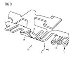
- the second integral member 10 ' which is shaped to provide the free end 11' with a predetermined movement in at least two mutually perpendicular planes is provided with the reference character B and in FIG. 3 shown in an enlarged view.
- FIG. 2 A first integral member 10 shaped to provide a predetermined movement in three mutually perpendicular planes is shown in FIG FIG. 2 shown.
- the member 10 is shaped that it extends meandering, and has a generally U-shaped loop 12.
- the sides of the U extend generally perpendicular to the adjacent portions of the member 10.
- the open side of the U-shaped loop 12 is disposed in the plane 14 of the member 10 , And the closed end of the U-shaped loop 12 is bent up out of the plane 14 of the member 10.
- the curved member 10 with its loop 12 allows movement of the free end 11 of the member 10 in the x-direction, y-direction and z-direction, as in FIG. 2 indicated.
- the free end 11 of the member 10 is divided into five fingers, each ending in a circular contact area.
- the circular contact areas 13 are arranged at the end of the free end 11 of the member 10 and movable in three mutually perpendicular planes, so that a spatial tolerance compensation is provided.
- a member 2 that extends generally in one direction such as a rectilinear rectangular member, may be in a single plane perpendicular to the top of the member, ie, in FIG FIG. 1 in the z direction, be movable.
- the free end 11 of the member 10 can now move not only in the z-direction, but also in the x-direction, by the width of the U-shaped loop 12th is opened and closed to compensate for differences in the distance of the free end 11 of the member 10 from the main part 3 of the rigid circuit board 1.
- the free end 11 of the member 10 can also move in the y-direction and is therefore movable in three mutually perpendicular planes.
- FIG. 3 is an enlarged view of the area B of FIG. 1 , Shown is a second member 10 'which is shaped to allow movement at the free end 11' of the member 10 'in three mutually perpendicular directions. As with the first member 10, the second member 10 ' also has a loop 12' in its length and a plurality of contact portions 13 'located at its free end 11'. The member 10 'extends generally in the x direction. The loop 12 'extends in the y-direction and is bent upwards out of the plane 14 of the member 10' in the z-direction.
- the limb generally extends in the xy plane and has a loop which extends generally in the y direction and is bent up in the z direction from the xy plane 14.
- the rigid circuit board 1 can be made by punching out the desired outer contour including the integral members 2, 10, 10 'and loops 12, 12' from a rectangular or square rigid circuit board.
- a member 10 with the loop 12 can then be further processed to bend out the closed end of the loop 12 from the plane 14 of the member 10 and thus allow movement at the free end 11 of the member 10 in three mutually perpendicular directions.
- the closed end of the loop may also be bent downwardly with respect to the plane 14 of the link 10 and upwardly as in FIG FIG. 4 shown.
- the rigid circuit board 1 further comprises a plurality of bent or deformed portions 15, which are the manufacture allow connections to other components whose position is determined by the particular application. These bent portions 15 may allow movement in a single direction, ie in the z-direction perpendicular to the top of the circuit board for the bent portions 15 extending in a link 2.
- a rigid circuit board 1 having stable, substantially immovable areas 15 and at least one member 10, 10 'which is shaped to allow movement in the free end 11, 11' of the member 10, 10 ' ,
- a rigid circuit board 1 with spatial tolerance can be provided without requiring a more expensive flexible circuit board material. Further, additional connections between a flexible circuit board and a rigid circuit board are avoided, so that the assembly costs are reduced.
Landscapes
- Engineering & Computer Science (AREA)
- Microelectronics & Electronic Packaging (AREA)
- Structure Of Printed Boards (AREA)
Abstract
Description
- Die Erfindung betrifft eine Schaltungsplatte und ein Verfahren zur Herstellung einer Schaltungsplatte.
- Schaltungsplatten, die auch üblicherweise als gedruckte Schaltungen oder Printplatten bezeichnet werden, bilden eine Struktur, mittels der elektrische Signale und/oder Strom von einem Punkt zu einem anderen Punkt über eine gewünschte Distanz übertragen werden können. Eine Schaltungsplatte kann auch die darauf montierten Komponenten mechanisch lagern. Schaltungsplatten besitzen typischerweise ein elektrisch isolierendes Substrat und eine Vielzahl von elektrisch leitenden Bahnen oder Leitungen, die auf dem elektrisch isolierenden Substrat in einem gewünschten Muster angeordnet sind, um die gewünschte Verdrahtungsanordnung zu bilden.
- Das Material des Substrates kann so ausgewählt werden, dass eine starre Schaltungsplatte vorgesehen wird. Beispielweise kann eine faserverstärkte Epoxidharzplatte oder eine Keramikplatte als Substrat Verwendung finden. Für einige Anwendungsfälle ist jedoch eine kompliziertere dreidimensionale Verdrahtungsstruktur erforderlich.
- Eine dreidimensionale Verdrahtungsstruktur kann mit Hilfe eines flexiblen Band- oder Foliensubstrates, wie beispielsweise einer Polyimidfolie, vorgesehen werden, das gebogen und/oder gefaltet werden kann, um eine flexible Schaltungsplatte auszubilden, die sich in drei Dimensionen erstreckt. Eine Anordnung, die zwei miteinander verriegelte flexible Schaltungsplatten für eine Flüssigkristallanzeige bildet, ist aus der
US 7,212,413 bekannt. - Obwohl flexible Schaltungsplatten den Vorteil besitzen, dass sie eine anpassungsfähige dreidimensionale Verdrahtungsstruktur bilden, sind flexible Schaltungsplatten gegenwärtig typischerweise teurer als starre Schaltungsplatten. Es ist generell wünschenswert, die Kosten von Komponenten zu reduzieren, um in der Lage zu sein, die Kosten der erzeugten Produkte zu verringern oder den Gewinn zu erhöhen.
- Es ist ein Ziel der vorliegenden Erfindung, eine Verdrahtungsstruktur mit geringen Kosten zu schaffen, die für eine Verwendung in einem großen Bereich von Anwendungsfällen geeignet ist.
- Dieses Ziel wird mit dem Gegenstand der unabhängigen Patentansprüche erreicht. Weitere vorteilhafte Ausführungsformen sind Gegenstand der abhängigen Ansprüche.
- Die Erfindung sieht eine starre Schaltungsplatte vor, die mindestens ein integrales Glied besitzt, das so ausgebildet ist, dass es eine vorgegebene Bewegung an einem freien Ende des Gliedes in mindestens zwei zueinander senkrechten Ebenen durchführen kann.
- Der hier verwendete Begriff "starr" soll eine flexible Schaltungsplatte auf Folien- oder Bandbasis, beispielsweise auf Basis eines Polyimidbandes, ausschließen. Der hier verwendete Begriff "integral" soll verdeutlichen, dass das Glied und der andere sich anschließende Abschnitt der starren Schaltungsplatte einstückig ausgebildet sind. Der verwendete Begriff "Glied" soll einen vorstehenden Bereich bezeichnen, der generell länglich ausgebildet ist.
- Es wird eine starre Schaltungsplatte vorgesehen, die aus Materialien hergestellt werden kann, welche mit geringeren Rohmaterialkosten verbunden sind, wobei die Schaltungsplatte gleichzeitig mindestens einen Bereich, insbesondere das freie Ende des integralen Gliedes, aufweist, der beweglich ist. Diese Bewegung kann dazu benutzt werden, um eine starre Schaltungsplatte mit räumlicher Toleranzkompensation vorzusehen, die durch das freie Ende des Gliedes erreicht wird.
- Beispielsweise kann die vorgegebene Bewegung kleine Änderungen in der Position einer Komponente, die auf der Schaltungsplatte montiert oder an diese angeschlossen werden soll, kompensieren. Diese Bewegung kann ferner vorgegeben sein, um eine räumliche Toleranz des freien Endes des Gliedes vorzusehen, wenn dieses freie Ende des Gliedes an einen zweiten Anschluss angepasst oder in einen Schlitz oder ein Durchgangsloch eingepasst werden soll.
- Steuersysteme für mechatronische Anwendungsfälle finden oft in aggressiven Umgebungen Verwendung, wie beispielsweise in einem Motor oder im heißen Öl des Getriebes. Die elektronischen Komponenten sind in einem abgedichteten Modul untergebracht, der einen Anschluss durch das Gehäuse des Moduls aufweist, damit die darin befindlichen Komponenten an weitere Komponenten außerhalb des Gehäuses angeschlossen werden können. Das bewegliche freie Ende des Gliedes kann für eine Dimensionstoleranz sorgen, um Variationen in der Herstelltoleranz des Gehäuses und/oder der starren Schaltungsplatte zu kompensieren, so dass das freie Ende des Gliedes in zuverlässiger Weise in den Anschluss im Gehäuse eingepasst werden kann.
- Das Glied ist so geformt, dass es eine Bewegung in mindestens zwei zueinander senkrechten Richtungen eines Bereiches des Gliedes durchführen kann, der in Bezug auf den geformten Bereich des Gliedes peripher ist. Insbesondere ist die Länge des Gliedes so ausgebildet, dass dieses eine Bewegung am freien Ende des Gliedes in mindestens zwei zueinander senkrechten Richtungen durchführen kann.
- Bei einer Ausführungsform umfasst das freie Ende des Gliedes mindestens einen Kontaktbereich. Dieser Kontaktbereich kann irgendeine wünschenswerte Form besitzen, beispielsweise als Kontaktpad oder Kontaktstift oder als Kontaktfassung ausgebildet sein.
- Der Kontaktbereich kann am am stärksten bewegbaren Abschnitt des Gliedes angeordnet sein, d. h. am freien Ende, um für eine zuverlässige elektrische Verbindung mit der starren Schaltungsplatte zu sorgen.
- Bei einer weiteren Ausführungsform ist das Glied so geformt, dass es eine vorgegebene Bewegung in drei zueinander senkrechten Ebenen durchführen kann. Das Glied kann auch so geformt sein, dass es für eine dreidimensionale Elastizität des freien Endes des Gliedes sorgt. Diese dreidimensionale Elastizität kann dazu dienen, einen guten elektrischen Kontakt zwischen einem Kontaktbereich am freien Ende und einer weiteren Komponente herzustellen, indem die elektrische Verbindung mit mindestens einem gewissen Federungsvermögen versehen wird.
- Das Glied kann auf eine Vielzahl von Weisen geformt sein, um für eine vorgesehene Bewegung am freien Ende des Gliedes zu sorgen. Beispielsweise kann die Länge des Gliedes eine Falte, eine Kinke und/oder einen verengten Abschnitt aufweisen.
- Bei einer Ausführungsform erstreckt sich das Glied in mindestens einer Schleife, wobei diese Schleife so geformt ist, dass sie für eine vorgegebene Bewegung am freien Ende des Gliedes sorgt. Das Glied ist daher nicht geradlinig ausgebildet, sondern besitzt eine mäandrierende Form.
- Bei der Schleife kann es sich um eine generell U-förmige Schleife mit einer offenen Seite und einer geschlossenen Seite handeln, wobei die offene Seite in der Ebene der starren Schaltungsplatte und das geschlossene Ende außerhalb der Ebene der Schaltungsplatte angeordnet sind.
- Eine derartige Form kann einfach hergestellt werden, indem die gewünschte Form der starren Schaltungsplatte ausgestanzt und dann die starre Schaltungsplatte im Bereich des geschlossenen Endes der Schleife gebogen wird. Eine starre Schaltungsplatte kann gebogen werden, indem sie um eine Formungseinheit gebogen wird. Während die starre Schaltungsplatte gebogen wird, kann auch Wärme aufgebracht werden.
- Die Schleife kann so gebogen werden, dass sie einen Krümmungsradius zwischen 5 mm und 30 mm besitzt. Der minimale Krümmungsradius, der möglich ist, ohne die Platte zu zerbrechen, kann von der Sprödigkeit der Materialien der starren Schaltungsplatte sowie von der Dicke der starren Schaltungsplatte abhängen. Der Krümmungsradius kann auch so ausgewählt sein, dass er für die gewünschte vorgegebene Bewegung sorgt.
- Die starre Schaltungsplatte der vorliegenden Anmeldung kann unter Verwendung einer herkömmlichen starren Schaltungsplatte geformt werden und kann ein elektrisch isolierendes Substrat umfassen, das einen oder mehrere der nachfolgenden Materialien aufweist: FR-2 (Phenolharzbaumwollpapier), FR-3 (Baumwollpapier und Epoxidharz), FR-4 (Glasgewebe und Epoxidharz), FR-5 (Glasgewebe und Epoxidharz), FR-6 (Matte-Glas und Polyester), G-10 (Glasgewebe und Epoxidharz), CEM-1 (Baumwollpapier und Epoxidharz), CEM-2 (Baumwollpapier und Epoxidharz), CEM-3 (Glasgewebe und Epoxidharz), CEM-4 (Glasgewebe und Epoxidharz), CEM-5 (Glasgewebe und Polyester).
- Die starre Schaltungsplatte kann einseitig ausgebildet sein und elektrisch leitende Bahnen aufweisen, die auf einer einzigen Seite eines elektrisch isolierenden starren Substrates angeordnet sind. Die starre Schaltungsplatte kann jedoch auch zweiseitig ausgebildet sein, wobei sich Bahnen auf beiden gegenüberliegenden Hauptflächen befinden, und kann des Weiteren elektrisch leitende Wege besitzen, um die Bahnen auf den zwei gegenüberliegenden Hauptflächen miteinander zu verbinden. Die starre Schaltungsplatte kann auch als Mehrschichtschaltungsplatte ausgebildet sein.
- Die Anmeldung sieht ferner ein mechatronisches Steuersystem vor, das eine starre Schaltungsplatte gemäß einer der vorstehend beschriebenen Ausführungsformen aufweist. Bei einer Ausführungsform handelt es sich bei dem mechatronischen Steuersystem um einen Steuermodul für ein automatisches Getriebe.
- Bei einer weiteren Ausführungsform umfasst die starre Schaltungsplatte eine Vielzahl von gebogenen Abschnitten, wobei elektronische Komponenten des mechatronischen Steuersystems auf den gebogenen Abschnitten angeordnet sind und/oder elektrisch hiermit verbunden sind. Die gebogenen Abschnitte können in einer vorgegebenen Weise bewegbar sein oder auch nicht. Die gebogenen Abschnitte können dazu dienen, um eine starre Schaltungsplatte mit einer dreidimensionalen Kontur zu schaffen. Eine dreidimensionale Kontur ermöglicht eine Anpassung der Form der starren Schaltungsplatte an die Position der mechanischen Komponenten.
- Die Anmeldung sieht ferner ein Verfahren zum Vorsehen einer räumlichen Toleranzkompensation in einer starren Schaltungsplatte vor. Eine starre Schaltungsplatte wird zur Verfügung gestellt, die mindestens ein integrales Glied besitzt. Das Glied ist so geformt, dass es für eine vorgegebene Bewegung eines freien Endes des Gliedes in mindestens zwei zueinander senkrechten Ebenen sorgt.
- Die starre Schaltungsplatte kann einfach hergestellt werden, so dass eine starre Schaltungsplatte vorgesehen werden kann, die mindestens einen beweglichen Abschnitt besitzt, der für eine räumliche Toleranz sorgt.
- Bei einer ersten Ausführungsform ist eine starre Vorläuferschaltungsplatte so geformt, dass das freie Ende des Gliedes den mindestens einen Kontaktbereich umfasst. Die starre Vorläuferschaltungsplatte kann so vorgesehen sein, dass sie einen generell quadratischen oder rechteckigen Umriss besitzt, der die gewünschte Verdrahtungsstruktur in der Form von elektrisch leitenden Bahnen und Kontaktbereichen aufweist. Eine Platte mit einem quadratischen oder rechteckigen Umriss ist einfacher und lässt sich billiger in großen Mengen herstellen.
- Diese starre Vorläuferschaltungsplatte kann dann so geformt werden, dass sie mindestens ein integrales Glied aufweist, und kann so geformt werden, dass mindestens ein Kontaktbereich an einem Ende des Gliedes vorgesehen ist.
- Die starre Vorläuferschaltungsplatte kann durch Stanzen geformt werden, um ein Glied vorzusehen und um ein Glied mit einer Schleife, die sich in der Ebene des Gliedes erstreckt, auszubilden.
- Nachdem die starre Schaltungsplatte mit dem mindestens einen integralen Glied aus der starren Vorläuferschaltungsplatte gestanzt worden ist, kann die Schleife in einer Richtung aus der Ebene des Gliedes herausgebogen werden. Mindestens ein Abschnitt der Schleife erstreckt sich daher in Richtung aus der Ebene des Gliedes heraus, um für eine Bewegung am freien Ende des Gliedes in mindestens zwei zueinander senkrechten Richtungen zu sorgen.
- Bei einer weiteren Ausführungsform ist die Schleife in einer Richtung aus der Ebene des Gliedes heraus auf permanente Weise gebogen, d. h. nach Druckabbau wird die Position des Gliedes außerhalb der Ebene zum größten Teil aufrechterhalten.
- In Verbindung mit den beigefügten Zeichnungen werden nunmehr Ausführungsformen der Erfindung beschrieben. Es zeigen:
- Figur 1
- eine perspektivische Ansicht einer starren Schaltungsplatte gemäß einer Ausführungsform,
- Figur 2
- eine vergrößerte Ansicht des Bereiches A in
Figur 1 , - Figur 3
- eine vergrößerte Ansicht des Bereiches B in
Figur 1 und - Figur 4
- eine schematische Teilschnittansicht einer starren Schaltungsplatte.
-
Figur 1 zeigt eine perspektivische Ansicht einer starren Schaltungsplatte 1 gemäß einer ersten Ausführungsform. - Die starre Schaltungsplatte 1 ist so geformt, dass sie eine Vielzahl von integralen Gliedern 2 aufweist, die sich von einem zentralen Bereich 3 aus erstrecken, der ein generell rechteckiges Durchgangsloch 4 zur Aufnahme eines nicht dargestellten elektronischen Moduls besitzt, welcher eine Vielzahl von elektronischen Komponenten aufweist.
- Die Struktur der starren Schaltungsplatte ist in der Teilschnittansicht der
Figur 4 gezeigt. Die starre Schaltungsplatte 1 umfasst ein dielektrisches Substrat 5 und eine Vielzahl von elektrisch leitenden Kupferbahnen 6 und Kontaktbereichen 7, die auf der Oberseite 8 des dielektrischen Substrates 6 angeordnet sind. Die Kupferbahnen sind mit einer weiteren Isolationsschicht 9 bedeckt, die die Kontaktbereiche 7 freilässt. Bei weiteren nichtdargestellten Ausführungsformen hat die starre Schaltungsplatte 1 eine doppelseitige Struktur oder eine Mehrschichtstruktur. - Die starre Schaltungsplatte 1 umfasst zwei integrale Glieder 10, 10', die so geformt sind, dass sie für eine vorgegebene Bewegung an einem freien Ende 11, 11' des Gliedes 10, 10' in mindestens zwei zueinander senkrechten Ebenen sorgen.
- Das erste Glied 10 mit einem freien Ende, das in mindestens zwei zueinander senkrechten Ebenen bewegbar ist, ist in
Figur 1 mit dem Bezugszeichen A versehen und inFigur 2 in einer vergrößerten Ansicht dargestellt. - Das zweite integrale Glied 10', das so geformt ist, dass es das freie Ende 11' mit einer vorgegebenen Bewegung in mindestens zwei zueinander senkrechten Ebenen versieht, ist mit dem Bezugszeichen B versehen und in
Figur 3 in einer vergrößerten Ansicht dargestellt. - Ein erstes integrales Glied 10, das so geformt ist, dass es eine vorgegebene Bewegung in drei zueinander senkrechten Ebenen vorsieht, ist in
Figur 2 gezeigt. Das Glied 10 ist so geformt, dass es sich mäanderförmig erstreckt, und besitzt eine generell U-förmige Schleife 12. Die Seiten des U's erstrecken sich generell senkrecht zu den benachbarten Bereichen des Gliedes 10. Die offene Seite der U-förmigen Schleife 12 ist in der Ebene 14 des Gliedes 10 angeordnet, und das geschlossene Ende der U-förmigen Schleife 12 ist nach oben aus der Ebene 14 des Gliedes 10 herausgebogen. Das gebogene Glied 10 mit seiner Schleife 12 ermöglicht eine Bewegung des freien Endes 11 des Gliedes 10 in x-Richtung, y-Richtung und z-Richtung, wie inFigur 2 angedeutet. - Bei dieser Ausführungsform ist das freie Ende 11 des Gliedes 10 in fünf Finger unterteilt, die jeweils in einem kreisförmigen Kontaktbereich enden. Die kreisförmigen Kontaktbereiche 13 sind am Ende des freien Endes 11 des Gliedes 10 angeordnet und in drei zueinander senkrechten Ebenen bewegbar, so dass eine räumliche Toleranzkompensation vorgesehen wird.
- Ein Glied 2, das sich generell in einer Richtung erstreckt, beispielsweise ein geradliniges rechteckförmiges Glied, kann in einer einzigen Ebene senkrecht zur Oberseite des Gliedes, d. h. in
Figur 1 in z-Richtung, bewegbar sein. Durch Anordnung einer Schleife 12, die sich in der Ebene des Gliedes 10 erstreckt, kann sich das freie Ende 11 des Gliedes 10 nunmehr nicht nur in z-Richtung, sondern auch in x-Richtung bewegen, indem die Breite der U-förmigen Schliefe 12 geöffnet und geschlossen wird, um Unterschiede im Abstand des freien Endes 11 des Gliedes 10 vom Hauptteil 3 der starren Schaltungsplatte 1 zu kompensieren. - Durch das Biegen des geschlossenen Endes der U-förmigen Schleife 12 aus der Ebene 14 des Gliedes 10 heraus kann sich das freie Ende 11 des Gliedes 10 auch in y-Richtung bewegen und ist daher in drei zueinander senkrechten Ebenen bewegbar.
-
Figur 3 ist eine vergrößerte Ansicht des Bereiches B derFigur 1 . Gezeigt ist ein zweites Glied 10', das so geformt ist, dass es eine Bewegung am freien Ende 11' des Gliedes 10' in drei zueinander senkrechten Richtungen ermöglicht. Wie bei dem ersten Glied 10 besitzt auch das zweite Glied 10' eine Schleife 12' in seiner Länge und eine Vielzahl von Kontaktbereichen 13', die an seinem freien Ende 11' angeordnet sind. Das Glied 10' erstreckt sich generell in x-Richtung. Die Schleife 12' erstreckt sich in y-Richtung und ist nach oben aus der Ebene 14 des Gliedes 10' in z-Richtung herausgebogen. - Für eine vereinfachte Darstellung sind die Bewegungsrichtungen in Verbindung mit der Teilschnittansicht eines Gliedes in
Figur 4 dargestellt. Das Glied erstreckt sich generell in der x-y-Ebene und besitzt eine Schleife, die sich generell in y-Richtung erstreckt und in z-Richtung aus der x-y-Ebene 14 nach oben herausgebogen ist. - Die starre Schaltungsplatte 1 kann hergestellt werden, indem die gewünschte Außenkontur einschließlich der integralen Glieder 2, 10, 10' und Schleifen 12, 12' aus einer rechteckigen oder quadratischen starren Schaltungsplatte herausgestanzt wird. Ein Glied 10 mit der Schleife 12 kann dann weiter bearbeitet werden, um das geschlossene Ende der Schleife 12 aus der Ebene 14 des Gliedes 10 herauszubiegen und damit eine Bewegung am freien Ende 11 des Gliedes 10 in drei zueinander senkrechten Richtungen zu ermöglichen. In der Ansicht der
Figur 4 kann das geschlossene Ende der Schleife in Bezug auf die Ebene 14 des Gliedes 10 auch abwärts gebogen sein sowie aufwärts wie inFigur 4 gezeigt. - Die starre Schaltungsplatte 1 umfasst ferner eine Vielzahl von gebogenen oder verformten Abschnitten 15, die die Herstellung von Anschlüssen an weitere Komponenten ermöglichen, deren Position durch den jeweiligen Anwendungsfall vorgegeben ist. Diese gebogenen Abschnitte 15 können eine Bewegung in einer einzigen Richtung ermöglichen, d. h. in z-Richtung senkrecht zur Oberseite der Schaltungsplatte für die sich in einem Glied 2 erstreckenden gebogenen Abschnitte 15.
- Es wird daher eine starre Schaltungsplatte 1 vorgesehen, die stabile, im Wesentlichen unbewegliche Bereiche 15 sowie mindestens ein Glied 10, 10' aufweist, das so geformt ist, dass es eine Bewegung im freien Ende 11, 11' des Gliedes 10, 10' ermöglicht. Eine starre Schaltungsplatte 1 mit räumlicher Toleranz kann vorgesehen werden, ohne dabei ein teureres flexibles Schaltungsplattenmaterial zu benötigen. Ferner werden zusätzliche Anschlüsse zwischen einer flexiblen Schaltungsplatte und einer starren Schaltungsplatte vermieden, so dass die Montagekosten verringert werden.
Claims (15)
- Starre Schaltungsplatte (1) mit mindestens einem integralen Glied (10; 10'), das so geformt ist, dass es eine vorgegebene Bewegung an einem freien Ende (11; 11') des Gliedes (10; 10') in mindestens zwei zueinander senkrechten Ebenen durchführen kann.
- Starre Schaltungsplatte (1) nach Anspruch 1, dadurch gekennzeichnet, dass das freie Ende (11; 11') des Gliedes (10; 10') mindestens einen Kontaktbereich (13) umfasst.
- Starres Schaltungsplatte (1) nach Anspruch 1 oder 2, dadurch gekennzeichnet, dass das Glied (10; 10') so geformt ist, dass es eine vorgegebene Bewegung am freien Ende des Gliedes (10; 10') in drei zueinander senkrechten Ebenen durchführen kann.
- Starre Schaltungsplatte (1) nach einem der Ansprüche 1-3, dadurch gekennzeichnet, dass das Glied (10; 10') so geformt ist, dass es für eine dreidimensionale Elastizität des freien Endes (11; 11') des Gliedes (10; 10') sorgt.
- Starre Schaltungsplatte (1) nach einem der Ansprüche 1-4, dadurch gekennzeichnet, dass sich das Glied (10; 10') in mindestens einer Schleife (12; 12') erstreckt.
- Starre Schaltungsplatte (1) nach einem der Ansprüche 1-5, dadurch gekennzeichnet, dass es sich bei der Schleife (12; 12') um eine generell U-förmige Schleife mit einer offenen Seite und einer geschlossenen Seite handelt, wobei die offene Seite in der Ebene (14) des Gliedes (10; 10') und das geschlossene Ende außerhalb der Ebene (14) des Gliedes (10; 10') angeordnet sind.
- Starre Schaltungsplatte (1) nach Anspruch 6, dadurch gekennzeichnet, dass die Schleife (12; 12') aus der Ebene (14) des Gliedes (10; 10') herausgebogen ist.
- Starre Schaltungsplatte (1) nach einem der Ansprüche 1-7, dadurch gekennzeichnet, dass die starre Schaltungsplatte (1) ein elektrisch isolierendes Substrat (5) aufweist, das eines der folgenden Materialien umfasst: FR-2 (Phenolharzbaumwollpapier), FR-3 (Baumwollpapier und Epoxidharz), FR-4 (Glasgewebe und Epoxidharz), FR-5 (Glasgewebe und Epoxidharz), FR-6 (Matte-Glas und Polyester), G-10 (Glasgewebe und Epoxidharz), CEM-1 (Baumwollpapier und Epoxidharz), CEM-2 (Baumwollpapier und Epoxidharz), CEM-3 (Glasgewebe und Epoxidharz), CEM-4 (Glasgewebe und Epoxidharz), CEM-5 (Glasgewebe und Polyester).
- Mechatronisches Steuersystem mit einer starren Schaltungsplatte (1) nach einem der Ansprüche 1-8.
- Mechatronisches Steuersystem nach Anspruch 9, dadurch gekennzeichnet, dass die starre Schaltungsplatte (1) eine Vielzahl von gebogenen Abschnitten (15) aufweist, wobei elektronische Komponenten des mechatronischen Steuersystems auf den gebogenen Abschnitten angeordnet und/oder hiermit elektrisch verbunden sind.
- Mechatronisches Steuersystem nach Anspruch 9 oder 10, dadurch gekennzeichnet, dass es ein Steuermodul eines automatischen Getriebes ist.
- Verfahren zu Herstellung einer Schaltungsplatte (1) mit den folgenden Schritten:Vorsehen einer starren Schaltungsplatte (1), die mindestens ein integrales Glied (10; 10') aufweist, undFormen des Gliedes (10; 10') derart, dass ein freies Ende (11; 11') des Gliedes (10; 10') eine vorgegebene Bewegung in mindestens zwei zueinander senkrechten Ebenen durchführen kann.
- Verfahren nach Anspruch 12, dadurch gekennzeichnet, dass eine starre Vorläuferschaltungsplatte so geformt wird, dass das freie Ende (11; 11') des Gliedes (10; 10') mindestens einen Kontaktbereich (13; 13') aufweist.
- Verfahren nach Anspruch 12 oder 13, dadurch gekennzeichnet, dass es des Weiteren das Stanzen einer starren Vorläuferschaltungsplatte (1) umfasst, um ein Glied (10; 10') mit einer Schleife (12; 12') vorzusehen, die sich in der Ebene (14) des Gliedes (10; 10') erstreckt.
- Verfahren nach Anspruch 14, dadurch gekennzeichnet, dass es des Weiteren das Biegen der Schleife (12; 12') in einer Richtung aus der Ebene (14) des Gliedes (10; 10') heraus umfasst.
Applications Claiming Priority (2)
| Application Number | Priority Date | Filing Date | Title |
|---|---|---|---|
| US11645008P | 2008-11-20 | 2008-11-20 | |
| DE102008058490A DE102008058490B3 (de) | 2008-11-21 | 2008-11-21 | Schaltungsplatte und Verfahren zur Herstellung einer Schaltungsplatte |
Publications (2)
| Publication Number | Publication Date |
|---|---|
| EP2190270A1 true EP2190270A1 (de) | 2010-05-26 |
| EP2190270B1 EP2190270B1 (de) | 2012-02-15 |
Family
ID=42055394
Family Applications (1)
| Application Number | Title | Priority Date | Filing Date |
|---|---|---|---|
| EP09174434A Not-in-force EP2190270B1 (de) | 2008-11-20 | 2009-10-29 | Schaltungsplatte und Verfahren zur Herstellung einer Schaltungsplatte |
Country Status (4)
| Country | Link |
|---|---|
| US (1) | US8294033B2 (de) |
| EP (1) | EP2190270B1 (de) |
| AT (1) | ATE546030T1 (de) |
| DE (1) | DE102008058490B3 (de) |
Families Citing this family (3)
| Publication number | Priority date | Publication date | Assignee | Title |
|---|---|---|---|---|
| US9084368B2 (en) * | 2011-06-15 | 2015-07-14 | Novatek Microelectronics Corp. | Single FPC board for connecting multiple modules and touch sensitive display module using the same |
| JP2013012270A (ja) * | 2011-06-29 | 2013-01-17 | Sanyo Electric Co Ltd | 光ピックアップ装置およびその製造方法 |
| DE102016002821A1 (de) * | 2016-03-05 | 2017-09-07 | Wabco Gmbh | Schaltkreis einer elektronischen Steuereinheit |
Citations (3)
| Publication number | Priority date | Publication date | Assignee | Title |
|---|---|---|---|---|
| DE2724399A1 (de) * | 1977-05-28 | 1978-11-30 | Martin Marietta Corp | Verfahren zur herstellung einer mehrschichtigen gedruckten schaltungsplatte mit integralen, flexiblen anschlusstuecken, sowie nach diesem verfahren gefertigte schaltungsplatte |
| DE2834525A1 (de) * | 1978-08-07 | 1980-02-14 | Loewe Opta Gmbh | Gedruckte schaltung auf flexiblem basismaterial mit von der hauptschaltungsachse abzweigenden auslegern zur intermodularen verbindung eines baugruppen aufweisenden fernsehgeraetechassis |
| US7212413B2 (en) | 2004-03-04 | 2007-05-01 | Au Optronics Corp. | Electronic device with flexible printed circuit board structure |
Family Cites Families (9)
| Publication number | Priority date | Publication date | Assignee | Title |
|---|---|---|---|---|
| US4758459A (en) | 1987-01-28 | 1988-07-19 | Northern Telecom Limited | Molded circuit board |
| US5495076A (en) * | 1993-10-18 | 1996-02-27 | Ford Motor Company | Flexible geometry circuit board |
| DE4412278A1 (de) * | 1994-04-09 | 1995-10-12 | Bosch Gmbh Robert | Starre und flexible Bereiche aufweisende Leiterplatte |
| US5518964A (en) | 1994-07-07 | 1996-05-21 | Tessera, Inc. | Microelectronic mounting with multiple lead deformation and bonding |
| DE29504736U1 (de) * | 1995-03-20 | 1995-07-27 | Siemens AG, 80333 München | Starrelastische Leiterplatte |
| US5903441A (en) * | 1997-09-24 | 1999-05-11 | Hewlett-Packard Company | Method and apparatus for aligning a printed circuit board with a chassis |
| US5984693A (en) | 1998-12-17 | 1999-11-16 | Hon Hai Precision Ind. Co., Ltd. | Contact of an LGA socket |
| DE19914418A1 (de) | 1999-03-30 | 2000-10-05 | Bosch Gmbh Robert | Leiterplatte mit starren und elastisch verformbaren Abschnitten und Gerät mit einer solchen Leiterplatte |
| JP4534503B2 (ja) * | 2004-01-30 | 2010-09-01 | 日立電線株式会社 | 光送受信モジュール |
-
2008
- 2008-11-21 DE DE102008058490A patent/DE102008058490B3/de not_active Expired - Fee Related
-
2009
- 2009-10-29 EP EP09174434A patent/EP2190270B1/de not_active Not-in-force
- 2009-10-29 AT AT09174434T patent/ATE546030T1/de active
- 2009-11-20 US US12/622,498 patent/US8294033B2/en not_active Expired - Fee Related
Patent Citations (3)
| Publication number | Priority date | Publication date | Assignee | Title |
|---|---|---|---|---|
| DE2724399A1 (de) * | 1977-05-28 | 1978-11-30 | Martin Marietta Corp | Verfahren zur herstellung einer mehrschichtigen gedruckten schaltungsplatte mit integralen, flexiblen anschlusstuecken, sowie nach diesem verfahren gefertigte schaltungsplatte |
| DE2834525A1 (de) * | 1978-08-07 | 1980-02-14 | Loewe Opta Gmbh | Gedruckte schaltung auf flexiblem basismaterial mit von der hauptschaltungsachse abzweigenden auslegern zur intermodularen verbindung eines baugruppen aufweisenden fernsehgeraetechassis |
| US7212413B2 (en) | 2004-03-04 | 2007-05-01 | Au Optronics Corp. | Electronic device with flexible printed circuit board structure |
Also Published As
| Publication number | Publication date |
|---|---|
| US20100122837A1 (en) | 2010-05-20 |
| ATE546030T1 (de) | 2012-03-15 |
| US8294033B2 (en) | 2012-10-23 |
| EP2190270B1 (de) | 2012-02-15 |
| DE102008058490B3 (de) | 2010-04-29 |
Similar Documents
| Publication | Publication Date | Title |
|---|---|---|
| DE112012002406B4 (de) | Dehnbare Schaltungsanordnungen | |
| DE69200500T2 (de) | Gestufte Mehrlagenverbindungsplatte und Herstellungsmethoden. | |
| EP0004899B1 (de) | Verfahren zur Herstellung elektrisch leitender und schwingungssicherer Verbindungen zwischen gedruckten Rückwandverdrahtungen von Leiterplatten und Kontaktfedern einer Federleiste, sowie hierfür geeignete Federleiste | |
| DE102012212223A1 (de) | Elektrische Verbinderanordnung zum Verbinden eines Elektronikmoduls und einer elektrischen Komponente | |
| DE10016064B4 (de) | Substrat,Einzelsubstrat und Verfahren zur Herstellung derselben | |
| DE112013006540T5 (de) | Verbinder mit versetzten Kontakten | |
| EP2198484B1 (de) | Elektrische schaltanordnung mit einem mid-schaltungsträger und einer damit verbundenen verbindungsschnittstelle | |
| WO2004030142A1 (de) | Übergang zwischen einer mikrostreifenleitung und einem hohlleiter | |
| EP0857351B1 (de) | Schalter mit flexibler leiterfolie als ortsfester kontakt und verbindung zu anschlusskontakten | |
| DE112017001259B4 (de) | Tragschienenbaugruppe mit einem Bussystem und einem eine Leiterplatte aufweisenden Elektronikgerät | |
| DE69200544T2 (de) | Integraler Randverbinder für Leiterkarten. | |
| DE10159113A1 (de) | Leiterplattenanordnung | |
| EP0575292A1 (de) | Verfahren zur Herstellung von Substraten mit Durchführungen | |
| EP2190270B1 (de) | Schaltungsplatte und Verfahren zur Herstellung einer Schaltungsplatte | |
| DE60013659T2 (de) | Schaltungsplatte mit seitlichen Verbindungen | |
| DE69500587T2 (de) | Verbinder für Leiterplatten | |
| EP3424283B1 (de) | Schaltkreis einer elektronischen steuereinheit | |
| DE60212299T2 (de) | Pin-grid-array elektrischer Steckverbinder | |
| EP0710432B1 (de) | Verfahren zur herstellung von folienleiterplatten oder halbzeugen für folienleiterplatten sowie nach dem verfahren hergestellte folienleiterplatten und halbzeuge | |
| DE102016107898B4 (de) | Laterale Leiterplattenverbindung | |
| DE102013109234B4 (de) | Leiterplatteneinheit mit Mitteln zur Kontaktierung eines Randkontaktsteckers | |
| WO2012171565A1 (de) | Elektrische kontakteinrichtung zur verbindung von leiterplatten | |
| EP0992065B1 (de) | Folie als träger von integrierten schaltungen | |
| DE102017126532A1 (de) | Leiterplattenverbund aus wenigstens zwei Leiterplatten | |
| WO2021115710A1 (de) | Elektronik-baugruppe |
Legal Events
| Date | Code | Title | Description |
|---|---|---|---|
| PUAI | Public reference made under article 153(3) epc to a published international application that has entered the european phase |
Free format text: ORIGINAL CODE: 0009012 |
|
| AK | Designated contracting states |
Kind code of ref document: A1 Designated state(s): AT BE BG CH CY CZ DE DK EE ES FI FR GB GR HR HU IE IS IT LI LT LU LV MC MK MT NL NO PL PT RO SE SI SK SM TR |
|
| AX | Request for extension of the european patent |
Extension state: AL BA RS |
|
| 17P | Request for examination filed |
Effective date: 20101126 |
|
| 17Q | First examination report despatched |
Effective date: 20110107 |
|
| RIC1 | Information provided on ipc code assigned before grant |
Ipc: H05K 1/00 20060101AFI20110615BHEP |
|
| GRAP | Despatch of communication of intention to grant a patent |
Free format text: ORIGINAL CODE: EPIDOSNIGR1 |
|
| GRAS | Grant fee paid |
Free format text: ORIGINAL CODE: EPIDOSNIGR3 |
|
| GRAA | (expected) grant |
Free format text: ORIGINAL CODE: 0009210 |
|
| AK | Designated contracting states |
Kind code of ref document: B1 Designated state(s): AT BE BG CH CY CZ DE DK EE ES FI FR GB GR HR HU IE IS IT LI LT LU LV MC MK MT NL NO PL PT RO SE SI SK SM TR |
|
| REG | Reference to a national code |
Ref country code: CH Ref legal event code: EP Ref country code: GB Ref legal event code: FG4D Free format text: NOT ENGLISH |
|
| REG | Reference to a national code |
Ref country code: IE Ref legal event code: FG4D Free format text: LANGUAGE OF EP DOCUMENT: GERMAN |
|
| REG | Reference to a national code |
Ref country code: AT Ref legal event code: REF Ref document number: 546030 Country of ref document: AT Kind code of ref document: T Effective date: 20120315 |
|
| REG | Reference to a national code |
Ref country code: DE Ref legal event code: R096 Ref document number: 502009002791 Country of ref document: DE Effective date: 20120412 |
|
| REG | Reference to a national code |
Ref country code: NL Ref legal event code: VDEP Effective date: 20120215 |
|
| LTIE | Lt: invalidation of european patent or patent extension |
Effective date: 20120215 |
|
| PG25 | Lapsed in a contracting state [announced via postgrant information from national office to epo] |
Ref country code: LT Free format text: LAPSE BECAUSE OF FAILURE TO SUBMIT A TRANSLATION OF THE DESCRIPTION OR TO PAY THE FEE WITHIN THE PRESCRIBED TIME-LIMIT Effective date: 20120215 Ref country code: NO Free format text: LAPSE BECAUSE OF FAILURE TO SUBMIT A TRANSLATION OF THE DESCRIPTION OR TO PAY THE FEE WITHIN THE PRESCRIBED TIME-LIMIT Effective date: 20120515 Ref country code: IS Free format text: LAPSE BECAUSE OF FAILURE TO SUBMIT A TRANSLATION OF THE DESCRIPTION OR TO PAY THE FEE WITHIN THE PRESCRIBED TIME-LIMIT Effective date: 20120615 Ref country code: NL Free format text: LAPSE BECAUSE OF FAILURE TO SUBMIT A TRANSLATION OF THE DESCRIPTION OR TO PAY THE FEE WITHIN THE PRESCRIBED TIME-LIMIT Effective date: 20120215 Ref country code: HR Free format text: LAPSE BECAUSE OF FAILURE TO SUBMIT A TRANSLATION OF THE DESCRIPTION OR TO PAY THE FEE WITHIN THE PRESCRIBED TIME-LIMIT Effective date: 20120215 |
|
| PG25 | Lapsed in a contracting state [announced via postgrant information from national office to epo] |
Ref country code: GR Free format text: LAPSE BECAUSE OF FAILURE TO SUBMIT A TRANSLATION OF THE DESCRIPTION OR TO PAY THE FEE WITHIN THE PRESCRIBED TIME-LIMIT Effective date: 20120516 Ref country code: LV Free format text: LAPSE BECAUSE OF FAILURE TO SUBMIT A TRANSLATION OF THE DESCRIPTION OR TO PAY THE FEE WITHIN THE PRESCRIBED TIME-LIMIT Effective date: 20120215 Ref country code: PL Free format text: LAPSE BECAUSE OF FAILURE TO SUBMIT A TRANSLATION OF THE DESCRIPTION OR TO PAY THE FEE WITHIN THE PRESCRIBED TIME-LIMIT Effective date: 20120215 Ref country code: PT Free format text: LAPSE BECAUSE OF FAILURE TO SUBMIT A TRANSLATION OF THE DESCRIPTION OR TO PAY THE FEE WITHIN THE PRESCRIBED TIME-LIMIT Effective date: 20120615 Ref country code: FI Free format text: LAPSE BECAUSE OF FAILURE TO SUBMIT A TRANSLATION OF THE DESCRIPTION OR TO PAY THE FEE WITHIN THE PRESCRIBED TIME-LIMIT Effective date: 20120215 |
|
| REG | Reference to a national code |
Ref country code: IE Ref legal event code: FD4D |
|
| PG25 | Lapsed in a contracting state [announced via postgrant information from national office to epo] |
Ref country code: CY Free format text: LAPSE BECAUSE OF FAILURE TO SUBMIT A TRANSLATION OF THE DESCRIPTION OR TO PAY THE FEE WITHIN THE PRESCRIBED TIME-LIMIT Effective date: 20120215 |
|
| PG25 | Lapsed in a contracting state [announced via postgrant information from national office to epo] |
Ref country code: SE Free format text: LAPSE BECAUSE OF FAILURE TO SUBMIT A TRANSLATION OF THE DESCRIPTION OR TO PAY THE FEE WITHIN THE PRESCRIBED TIME-LIMIT Effective date: 20120215 Ref country code: DK Free format text: LAPSE BECAUSE OF FAILURE TO SUBMIT A TRANSLATION OF THE DESCRIPTION OR TO PAY THE FEE WITHIN THE PRESCRIBED TIME-LIMIT Effective date: 20120215 Ref country code: IE Free format text: LAPSE BECAUSE OF FAILURE TO SUBMIT A TRANSLATION OF THE DESCRIPTION OR TO PAY THE FEE WITHIN THE PRESCRIBED TIME-LIMIT Effective date: 20120215 Ref country code: CZ Free format text: LAPSE BECAUSE OF FAILURE TO SUBMIT A TRANSLATION OF THE DESCRIPTION OR TO PAY THE FEE WITHIN THE PRESCRIBED TIME-LIMIT Effective date: 20120215 Ref country code: RO Free format text: LAPSE BECAUSE OF FAILURE TO SUBMIT A TRANSLATION OF THE DESCRIPTION OR TO PAY THE FEE WITHIN THE PRESCRIBED TIME-LIMIT Effective date: 20120215 Ref country code: SI Free format text: LAPSE BECAUSE OF FAILURE TO SUBMIT A TRANSLATION OF THE DESCRIPTION OR TO PAY THE FEE WITHIN THE PRESCRIBED TIME-LIMIT Effective date: 20120215 Ref country code: EE Free format text: LAPSE BECAUSE OF FAILURE TO SUBMIT A TRANSLATION OF THE DESCRIPTION OR TO PAY THE FEE WITHIN THE PRESCRIBED TIME-LIMIT Effective date: 20120215 |
|
| PG25 | Lapsed in a contracting state [announced via postgrant information from national office to epo] |
Ref country code: IT Free format text: LAPSE BECAUSE OF FAILURE TO SUBMIT A TRANSLATION OF THE DESCRIPTION OR TO PAY THE FEE WITHIN THE PRESCRIBED TIME-LIMIT Effective date: 20120215 Ref country code: SK Free format text: LAPSE BECAUSE OF FAILURE TO SUBMIT A TRANSLATION OF THE DESCRIPTION OR TO PAY THE FEE WITHIN THE PRESCRIBED TIME-LIMIT Effective date: 20120215 |
|
| PLBE | No opposition filed within time limit |
Free format text: ORIGINAL CODE: 0009261 |
|
| STAA | Information on the status of an ep patent application or granted ep patent |
Free format text: STATUS: NO OPPOSITION FILED WITHIN TIME LIMIT |
|
| 26N | No opposition filed |
Effective date: 20121116 |
|
| REG | Reference to a national code |
Ref country code: DE Ref legal event code: R097 Ref document number: 502009002791 Country of ref document: DE Effective date: 20121116 |
|
| BERE | Be: lapsed |
Owner name: CONTINENTAL AUTOMOTIVE G.M.B.H. Effective date: 20121031 |
|
| PG25 | Lapsed in a contracting state [announced via postgrant information from national office to epo] |
Ref country code: ES Free format text: LAPSE BECAUSE OF FAILURE TO SUBMIT A TRANSLATION OF THE DESCRIPTION OR TO PAY THE FEE WITHIN THE PRESCRIBED TIME-LIMIT Effective date: 20120526 |
|
| PG25 | Lapsed in a contracting state [announced via postgrant information from national office to epo] |
Ref country code: MC Free format text: LAPSE BECAUSE OF NON-PAYMENT OF DUE FEES Effective date: 20121031 |
|
| PG25 | Lapsed in a contracting state [announced via postgrant information from national office to epo] |
Ref country code: BG Free format text: LAPSE BECAUSE OF FAILURE TO SUBMIT A TRANSLATION OF THE DESCRIPTION OR TO PAY THE FEE WITHIN THE PRESCRIBED TIME-LIMIT Effective date: 20120515 Ref country code: BE Free format text: LAPSE BECAUSE OF NON-PAYMENT OF DUE FEES Effective date: 20121031 |
|
| PG25 | Lapsed in a contracting state [announced via postgrant information from national office to epo] |
Ref country code: MT Free format text: LAPSE BECAUSE OF FAILURE TO SUBMIT A TRANSLATION OF THE DESCRIPTION OR TO PAY THE FEE WITHIN THE PRESCRIBED TIME-LIMIT Effective date: 20120215 |
|
| PG25 | Lapsed in a contracting state [announced via postgrant information from national office to epo] |
Ref country code: TR Free format text: LAPSE BECAUSE OF FAILURE TO SUBMIT A TRANSLATION OF THE DESCRIPTION OR TO PAY THE FEE WITHIN THE PRESCRIBED TIME-LIMIT Effective date: 20120215 |
|
| PG25 | Lapsed in a contracting state [announced via postgrant information from national office to epo] |
Ref country code: SM Free format text: LAPSE BECAUSE OF FAILURE TO SUBMIT A TRANSLATION OF THE DESCRIPTION OR TO PAY THE FEE WITHIN THE PRESCRIBED TIME-LIMIT Effective date: 20120215 Ref country code: LU Free format text: LAPSE BECAUSE OF NON-PAYMENT OF DUE FEES Effective date: 20121029 |
|
| REG | Reference to a national code |
Ref country code: CH Ref legal event code: PL |
|
| GBPC | Gb: european patent ceased through non-payment of renewal fee |
Effective date: 20131029 |
|
| PG25 | Lapsed in a contracting state [announced via postgrant information from national office to epo] |
Ref country code: HU Free format text: LAPSE BECAUSE OF FAILURE TO SUBMIT A TRANSLATION OF THE DESCRIPTION OR TO PAY THE FEE WITHIN THE PRESCRIBED TIME-LIMIT Effective date: 20091029 Ref country code: LI Free format text: LAPSE BECAUSE OF NON-PAYMENT OF DUE FEES Effective date: 20131031 Ref country code: CH Free format text: LAPSE BECAUSE OF NON-PAYMENT OF DUE FEES Effective date: 20131031 Ref country code: GB Free format text: LAPSE BECAUSE OF NON-PAYMENT OF DUE FEES Effective date: 20131029 |
|
| PG25 | Lapsed in a contracting state [announced via postgrant information from national office to epo] |
Ref country code: MK Free format text: LAPSE BECAUSE OF FAILURE TO SUBMIT A TRANSLATION OF THE DESCRIPTION OR TO PAY THE FEE WITHIN THE PRESCRIBED TIME-LIMIT Effective date: 20120215 |
|
| REG | Reference to a national code |
Ref country code: FR Ref legal event code: PLFP Year of fee payment: 7 |
|
| REG | Reference to a national code |
Ref country code: AT Ref legal event code: MM01 Ref document number: 546030 Country of ref document: AT Kind code of ref document: T Effective date: 20141029 |
|
| PG25 | Lapsed in a contracting state [announced via postgrant information from national office to epo] |
Ref country code: AT Free format text: LAPSE BECAUSE OF NON-PAYMENT OF DUE FEES Effective date: 20141029 |
|
| REG | Reference to a national code |
Ref country code: FR Ref legal event code: PLFP Year of fee payment: 8 |
|
| REG | Reference to a national code |
Ref country code: FR Ref legal event code: PLFP Year of fee payment: 9 |
|
| REG | Reference to a national code |
Ref country code: FR Ref legal event code: PLFP Year of fee payment: 10 |
|
| PGFP | Annual fee paid to national office [announced via postgrant information from national office to epo] |
Ref country code: DE Payment date: 20181031 Year of fee payment: 10 |
|
| PGFP | Annual fee paid to national office [announced via postgrant information from national office to epo] |
Ref country code: FR Payment date: 20191028 Year of fee payment: 11 |
|
| REG | Reference to a national code |
Ref country code: DE Ref legal event code: R119 Ref document number: 502009002791 Country of ref document: DE |
|
| REG | Reference to a national code |
Ref country code: DE Ref legal event code: R081 Ref document number: 502009002791 Country of ref document: DE Owner name: VITESCO TECHNOLOGIES GMBH, DE Free format text: FORMER OWNER: CONTINENTAL AUTOMOTIVE GMBH, 30165 HANNOVER, DE |
|
| PG25 | Lapsed in a contracting state [announced via postgrant information from national office to epo] |
Ref country code: DE Free format text: LAPSE BECAUSE OF NON-PAYMENT OF DUE FEES Effective date: 20200501 |
|
| PG25 | Lapsed in a contracting state [announced via postgrant information from national office to epo] |
Ref country code: FR Free format text: LAPSE BECAUSE OF NON-PAYMENT OF DUE FEES Effective date: 20201031 |