EP2175504A1 - Organic electroluminescence element and method for manufacturing the same - Google Patents
Organic electroluminescence element and method for manufacturing the same Download PDFInfo
- Publication number
- EP2175504A1 EP2175504A1 EP08791538A EP08791538A EP2175504A1 EP 2175504 A1 EP2175504 A1 EP 2175504A1 EP 08791538 A EP08791538 A EP 08791538A EP 08791538 A EP08791538 A EP 08791538A EP 2175504 A1 EP2175504 A1 EP 2175504A1
- Authority
- EP
- European Patent Office
- Prior art keywords
- layer
- organic
- leakage current
- current block
- electrode
- Prior art date
- Legal status (The legal status is an assumption and is not a legal conclusion. Google has not performed a legal analysis and makes no representation as to the accuracy of the status listed.)
- Withdrawn
Links
Images

Classifications
-
- H—ELECTRICITY
- H10—SEMICONDUCTOR DEVICES; ELECTRIC SOLID-STATE DEVICES NOT OTHERWISE PROVIDED FOR
- H10K—ORGANIC ELECTRIC SOLID-STATE DEVICES
- H10K59/00—Integrated devices, or assemblies of multiple devices, comprising at least one organic light-emitting element covered by group H10K50/00
- H10K59/10—OLED displays
- H10K59/12—Active-matrix OLED [AMOLED] displays
- H10K59/122—Pixel-defining structures or layers, e.g. banks
-
- H—ELECTRICITY
- H10—SEMICONDUCTOR DEVICES; ELECTRIC SOLID-STATE DEVICES NOT OTHERWISE PROVIDED FOR
- H10D—INORGANIC ELECTRIC SEMICONDUCTOR DEVICES
- H10D30/00—Field-effect transistors [FET]
- H10D30/60—Insulated-gate field-effect transistors [IGFET]
- H10D30/67—Thin-film transistors [TFT]
- H10D30/6704—Thin-film transistors [TFT] having supplementary regions or layers in the thin films or in the insulated bulk substrates for controlling properties of the device
- H10D30/6706—Thin-film transistors [TFT] having supplementary regions or layers in the thin films or in the insulated bulk substrates for controlling properties of the device for preventing leakage current
-
- H—ELECTRICITY
- H10—SEMICONDUCTOR DEVICES; ELECTRIC SOLID-STATE DEVICES NOT OTHERWISE PROVIDED FOR
- H10K—ORGANIC ELECTRIC SOLID-STATE DEVICES
- H10K50/00—Organic light-emitting devices
-
- H—ELECTRICITY
- H10—SEMICONDUCTOR DEVICES; ELECTRIC SOLID-STATE DEVICES NOT OTHERWISE PROVIDED FOR
- H10K—ORGANIC ELECTRIC SOLID-STATE DEVICES
- H10K50/00—Organic light-emitting devices
- H10K50/10—OLEDs or polymer light-emitting diodes [PLED]
- H10K50/11—OLEDs or polymer light-emitting diodes [PLED] characterised by the electroluminescent [EL] layers
-
- H—ELECTRICITY
- H10—SEMICONDUCTOR DEVICES; ELECTRIC SOLID-STATE DEVICES NOT OTHERWISE PROVIDED FOR
- H10K—ORGANIC ELECTRIC SOLID-STATE DEVICES
- H10K59/00—Integrated devices, or assemblies of multiple devices, comprising at least one organic light-emitting element covered by group H10K50/00
- H10K59/10—OLED displays
- H10K59/17—Passive-matrix OLED displays
- H10K59/173—Passive-matrix OLED displays comprising banks or shadow masks
-
- H—ELECTRICITY
- H10—SEMICONDUCTOR DEVICES; ELECTRIC SOLID-STATE DEVICES NOT OTHERWISE PROVIDED FOR
- H10K—ORGANIC ELECTRIC SOLID-STATE DEVICES
- H10K71/00—Manufacture or treatment specially adapted for the organic devices covered by this subclass
-
- H—ELECTRICITY
- H10—SEMICONDUCTOR DEVICES; ELECTRIC SOLID-STATE DEVICES NOT OTHERWISE PROVIDED FOR
- H10K—ORGANIC ELECTRIC SOLID-STATE DEVICES
- H10K71/00—Manufacture or treatment specially adapted for the organic devices covered by this subclass
- H10K71/10—Deposition of organic active material
- H10K71/12—Deposition of organic active material using liquid deposition, e.g. spin coating
- H10K71/13—Deposition of organic active material using liquid deposition, e.g. spin coating using printing techniques, e.g. ink-jet printing or screen printing
- H10K71/135—Deposition of organic active material using liquid deposition, e.g. spin coating using printing techniques, e.g. ink-jet printing or screen printing using ink-jet printing
-
- H—ELECTRICITY
- H10—SEMICONDUCTOR DEVICES; ELECTRIC SOLID-STATE DEVICES NOT OTHERWISE PROVIDED FOR
- H10K—ORGANIC ELECTRIC SOLID-STATE DEVICES
- H10K71/00—Manufacture or treatment specially adapted for the organic devices covered by this subclass
- H10K71/10—Deposition of organic active material
- H10K71/191—Deposition of organic active material characterised by provisions for the orientation or alignment of the layer to be deposited
-
- H—ELECTRICITY
- H10—SEMICONDUCTOR DEVICES; ELECTRIC SOLID-STATE DEVICES NOT OTHERWISE PROVIDED FOR
- H10K—ORGANIC ELECTRIC SOLID-STATE DEVICES
- H10K71/00—Manufacture or treatment specially adapted for the organic devices covered by this subclass
- H10K71/40—Thermal treatment, e.g. annealing in the presence of a solvent vapour
-
- H—ELECTRICITY
- H10—SEMICONDUCTOR DEVICES; ELECTRIC SOLID-STATE DEVICES NOT OTHERWISE PROVIDED FOR
- H10K—ORGANIC ELECTRIC SOLID-STATE DEVICES
- H10K2101/00—Properties of the organic materials covered by group H10K85/00
- H10K2101/40—Interrelation of parameters between multiple constituent active layers or sublayers, e.g. HOMO values in adjacent layers
-
- H—ELECTRICITY
- H10—SEMICONDUCTOR DEVICES; ELECTRIC SOLID-STATE DEVICES NOT OTHERWISE PROVIDED FOR
- H10K—ORGANIC ELECTRIC SOLID-STATE DEVICES
- H10K2102/00—Constructional details relating to the organic devices covered by this subclass
- H10K2102/301—Details of OLEDs
- H10K2102/341—Short-circuit prevention
-
- H—ELECTRICITY
- H10—SEMICONDUCTOR DEVICES; ELECTRIC SOLID-STATE DEVICES NOT OTHERWISE PROVIDED FOR
- H10K—ORGANIC ELECTRIC SOLID-STATE DEVICES
- H10K50/00—Organic light-emitting devices
- H10K50/10—OLEDs or polymer light-emitting diodes [PLED]
- H10K50/17—Carrier injection layers
Definitions
- the organic layer 90 (the hole injection layer 40 and the light-emitting layer 60) creeps up the inclined surface of the bank 30 at a boundary region between the organic layer 90 and the bank 30.
- This creep-up portion is formed by reducing the liquid repellency of a bank.
- the creep-up portion refers to a portion of a film formed into such a shape creeping up an inclined surface through film formation.
- the resistivity of the hole injection layer 40 is not so high compared with the resistivity of the light-emitting layer 60 or the like.
- leakage current may flow between an upper electrode 70 and the lower electrodes 20.
- the above method that is, a method that inserts an inorganic insulating layer such as silicon oxide covering the periphery of a lower electrode between the lower electrode and a bank is not effective for leakage current that flows in such a pathway.
- the leakage current block layer 5 is formed on the first surface of the hole injection layer 4 at the boundary region R12 by making the leakage current block layer 5 creep up the inclined surface of the hole injection layer 4 formed at the inner peripheral side surface of the pixel region R11.
- a creep-up portion 5a of the leak current block layer 5 creeps up to reach a higher position than the inclined surface formed with a creep-up portion 4a of the hole injection layer 4, so as to totally cover the creep-up portion 4a of the hole injection layer 4.
- the lower end 5b of the leakage current block layer 5 is also repelled by the hole injection layer 4 and backs off to the position near outer periphery of the pixel region R11.
- the liquid repellency on the surface of the bank 3 is reduced properly by performing a lyophilic treatment, and then an ink droplet for a leakage current block layer is discharged in the inside region of the boundary region R12 or the pixel region R11 by the ink-jet method.
- the edge of the leakage current block layer 6 is spontaneously arranged on the inclined surface of the bank.
- a publicly know material may be used and those examples may include oxadiazol or derivatives thereof, anthraquinodimethane or derivatives thereof, benzoquinone or derivatives thereof, naphthoquinone or derivatives thereof, anthraquinone or derivatives thereof, tetracyanoanthraquinonedimethane or derivatives thereof, fluorenone or derivatives thereof, diphenyldicyanoethylene or derivatives thereof, diphenoquinone or derivatives thereof, 8-hydroxyquinoline or metal complexes of its derivatives, polyquinoline or derivatives thereof, polyquinoxaline or derivatives thereof, and polyfluorene or derivatives thereof.
- Examples of the metals in the group IIA of the periodic table except for Ca and having a work function of 1.5 to 3.0 electron volts, or oxide, halide, or carbonate of those metals may include: strontium, magnesium oxide, magnesium fluoride, strontium fluoride, barium fluoride, strontium oxide, and magnesium carbonate.
- PEDOT (CH8000LVW185; manufactured by H.C. Starck GmbH) was mixed with 2 weight percent of 2-butoxyethanol and then the mixture was filtered through a 0.45 micrometer filter, and the resultant was used for a hole injection layer.
- Ink-jet coating was performed by using the 80L (manufactured by Liter Corporation). At this time, droplets were applied at even intervals, and the number of the droplets per pixel were four droplets. After this application, the vacuum drying was performed.
- the hole injection layer made of PEDOT had the resistivity of 1 ⁇ 10 5 ohm centimeters to 3 ⁇ 10 5 ohm centimeters.
- Ink-jet coating was performed using ink in which a heat/photo curable insulating polymer 1 was dissolved in an organic solvent and by using the 120L (manufactured by Litrex Corporation).
- DPHA dipentaerythritol hexaacrylate
- Irgacure907 manufactured by Ciba Speciality Chemicals Corporation
- the present example corresponds to the second embodiment, and is in the case where the leakage current block layer is formed only at the curved portions of the pixel.
- Example 2 An element was produced in the same manner as the Example 1 except that the ink of the insulating polymer 1 was not formed at the whole periphery of the pixel but was formed only at the curved portions of a pixel at the step of forming the leakage current block layer in the Example 1. In this case, one droplet was discharged only at each of the curved portions of the pixel (at two positions per pixel).
- the organic EL element of the second example can reduce the ink amount compared with that of the Example 1.
Landscapes
- Engineering & Computer Science (AREA)
- Manufacturing & Machinery (AREA)
- Physics & Mathematics (AREA)
- Optics & Photonics (AREA)
- Microelectronics & Electronic Packaging (AREA)
- Electroluminescent Light Sources (AREA)
- Devices For Indicating Variable Information By Combining Individual Elements (AREA)
Abstract
Description
- The present invention relates to an organic electroluminescence element (hereinafter, may be referred to as an organic EL element) and a method for manufacturing the organic EL element, and more particularly, to a structure for preventing leakage current from the organic EL element.
- Organic EL elements are formed on substrates made of glass, plastic (including films), silicon wafers, or the like. Generally, organic EL elements have a stacked structure comprising a lower electrode, an upper electrode, and an organic layer disposed between the lower electrodes and the upper electrodes. The organic layer have a light-emitting layer made of light-emitting materials, as necessary, hole transport layers and/or electron transport layers and the like. When voltage is applied between the upper electrode and the lower electrode of the organic EL element to flow electric current, carriers (electrons and holes) injected from both electrodes are recombined in the light-emitting layers, which leads to light emission from the light-emitting layers.
- In such organic EL elements, forming banks directly on the lower electrodes allows to enhance patterning accuracy of organic layers (ink). On the other hand, the thicknesses of the organic layers may become small at boundary portions between the banks and the lower electrodes due to repelling of ink droplets at the side surfaces of the banks. To avoid this problem, for example,
Patent Document 1 refers a structure in which an inorganic insulating layer such as silicon oxide covering the periphery of a lower electrode is inserted between the lower electrode and a bank. In this method, because the inorganic insulating layer is formed by covering a boundary portion between the bank and the lower electrode, a dielectric strength voltage at the boundary portion between the bank and the lower electrode can be enhanced, which enables to suppress electric leak. - Patent Document 1:
JP 2005-203215 A - However, the method in
Patent Document 1 requires to form the inorganic insulating layer generally by a process using a vacuum apparatus, such as a chemical vapor deposition (CVD) method and a sputtering method, prior to a process of forming an organic layer by an ink-jet method. Therefore, the method inPatent Document 1 has problems that a costly equipment investment is required and that its application to large screens is difficult. Furthermore, this method has another problem that the method does not effectively work on leakage current that flows through a hole injection layer as explained below. -
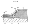
Fig. 6 is a sectional view of a state in which leakage current flows through a hole injection layer of a conventional organic EL element. In anorganic EL element 100 shown inFig. 6 , a plurality oflower electrodes 20 are formed on aglass substrate 10, and abank 30 is provided between the neighboringlower electrodes 20 so as to surround each of thelower electrodes 20. Thebank 30 is formed on the periphery of each of the neighboringlower electrodes 20. An organic layer 90 (ahole injection layer 40 and a light-emitting layer 60) is formed at an opening of thebank 30 by an ink-jet method. Anupper electrode 70 is formed on the upper surfaces of theorganic layer 90 and thebank 30. - As shown in
Fig. 6 , the organic layer 90 (thehole injection layer 40 and the light-emitting layer 60) creeps up the inclined surface of thebank 30 at a boundary region between theorganic layer 90 and thebank 30. This creep-up portion is formed by reducing the liquid repellency of a bank. The creep-up portion refers to a portion of a film formed into such a shape creeping up an inclined surface through film formation. The resistivity of thehole injection layer 40 is not so high compared with the resistivity of the light-emittinglayer 60 or the like. As a result, as shown inFig. 6 with an arrow C, leakage current may flow between anupper electrode 70 and thelower electrodes 20. The above method, that is, a method that inserts an inorganic insulating layer such as silicon oxide covering the periphery of a lower electrode between the lower electrode and a bank is not effective for leakage current that flows in such a pathway. - In view of the foregoing, the present invention has been made, and it is an object of the present invention to provide an organic EL element that suppresses leakage current flowing between an upper electrode and a lower electrode through an organic layer at a boundary region between a pixel region and a bank region, and a method for producing the organic EL element.
- The present invention provides an organic EL device that employs the following structure and a method for producing the device.
- [1] An organic electroluminescence element comprising:
- a first electrode provided near to a substrate;
- a second electrode provided at the side of the first electrode opposite to the substrate, and paired with the first electrode;
- an organic layer held between the first electrode and the second electrode, and comprising at least one light-emitting layer;
- a leakage current block layer formed between the first electrode and the second electrode and at a boundary region between the organic layer and a bank,
being at a pixel region surrounded by the bank provided on the substrate. - [2] The organic electroluminescence element according to the above [1] , wherein the leakage current block layer is formed by an ink-jet method.
- [3] The organic electroluminescence element according to the above [1] or [2], wherein the boundary region viewed from the thickness direction of the substrate has a substantially elliptical shape which has two straight portions that are substantially linear and face substantially parallel to each other, and the leakage current block layer is formed at curved portions which is at except the two straight portions from the boundary region.
- [4] The organic electroluminescence element according to any one of the above [1] to [3], wherein the organic layer has a hole injection layer;
the hole injection layer is formed by an ink-jet method configured to form a creep-up portion along an inclined surface of the bank;
and the leakage current block layer is provided between the creep-up portion of the hole injection layer and the second electrode. - [5] The organic electroluminescence element according to any one of the above [1] to [3], wherein the light-emitting layer is formed by an ink-jet method configured to form a creep-up portion along an inclined surface of the bank,
and the leakage current block layer is provided between the creep-up portion of the light-emitting layer and the second electrode. - [6] The organic electroluminescence element according to any one of the above [1] to [5], wherein the width of the leakage current block layer in a direction from the bank to the center of the pixel region viewed from the thickness direction of the substrate is 1 micrometer or more to 10 micrometers or less.
- [7] The organic electroluminescence element according to any one of the above [1] to [5], wherein the leakage current block layer has a resistivity of 106 or more ohm centimeters.
- [8] The organic electroluminescence element according to any one of the above [1] to [5], wherein the leakage current block layer is a polymer resin crosslinked with heat or light.
- [9] A method for producing an organic electroluminescence element, which has a first electrode provided near to a substrate, a second electrode provided at the side of the first electrode opposite to the substrate and paired with the first electrode, and an organic layer held between the first electrode and the second electrode and comprising at least one light-emitting layer, and which is at a pixel region surrounded by a bank provided on a substrate, the method comprising:
- discharging an organic material in the pixel region by an ink-jet method and forming a leakage current block layer between the first electrode and the second electrode, at a boundary region between the organic layer and the bank, so that electric resistance of the leakage current block layer in a thickness direction of the substrate is higher than an electric resistance of the organic layer sandwiched with the first electrode in the thickness direction of the substrate.
- [10] The method for producing an organic electroluminescence element according to the above [9],
wherein at the forming the leakage current block layer, the leakage current block layer is stacked on a surface of a hole injection layer at the boundary region between the organic layer and the bank by making the organic material creep up along an inclined surface of the hole injection layer utilizing a property of the organic material that is repelled from the hole injection layer comprised in the organic layer. - [11] The method for producing an organic electroluminescence element according to the above [9],
wherein at the forming the leakage current block layer, an edge of the leakage current block layer is formed on an inclined surface of the hole injection layer formed at an inner peripheral side surface of the pixel region, by dropping a droplet containing the organic material at the boundary region or the pixel region. - [12] The method for producing an organic electroluminescence element according to the above [9],
wherein at the forming the leakage current block layer, the leakage current block layer is formed on a surface of the light-emitting layer at the boundary region between the organic layer and the bank by making the organic material creep up along an inclined surface of the light-emitting layer utilizing a property of the organic material that is repelled from the light-emitting layer comprising in the organic layer. - [13] The method for producing an organic electroluminescence element according to the above [9],
wherein at the forming the leakage current block layer, an edge of the leakage current block layer is formed on an inclined surface of the light-emitting layer formed at an inner peripheral side surface of the pixel region, by dropping a droplet containing the organic material at the boundary region or the pixel region. - [14] The method for producing an organic electroluminescence element according to any one of the above [9] to [13], wherein the forming the leakage current block layer comprises discharging ink in which an organic solvent as the organic material is contained as a main component by the ink-jet method, and thereafter crosslinking the ink by heat and/or light, thereby forming the leakage current block layer.
- [15] The method for producing an organic electroluminescence element according to any one of the above [9] to [14], wherein the organic layer comprises the hole injection layer and the hole injection layer is formed by the ink-jet method.
- [14] The method for producing an organic electroluminescence element according to any one of the above [9] to [15], wherein the light-emitting layer is formed by the ink-jet method.
- The organic EL element of the present invention performs an effect that surely suppresses leakage current flowing between the first electrode and the second electrode through the organic layer at the boundary region since it has a leakage current block layer that is formed from an organic material having a higher resistance than that of an organic layer and is formed between a first electrode and a second electrode at a boundary region between a pixel region and a bank region.
- According to the method for producing the organic EL element of the present invention, it is possible to form the leakage current block layer easily and properly since the leakage current block layer is formed by discharging an organic material having a higher resistance than that of an organic layer by an ink-jet method.
-
- [
Fig. 1] Fig. 1 is a sectional view in the direction of arrows A-A ofFig. 2 of a portion of a pixel region of the first embodiment of the organic EL element according to the present invention. - [
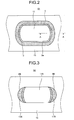
Fig. 2] Fig. 2 is a diagram of the pixel region of the organic EL element viewed from the opening side of the concave portion of the element. - [
Fig. 3] Fig. 3 is a diagram of a pixel region of the second embodiment of the organic EL element according to the present invention viewed from the opening side of a concave portion of the element. - [
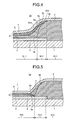
Fig. 4] Fig. 4 is a sectional view of a portion of a pixel region of the third embodiment of the organic EL element according to the present invention. - [
Fig. 5] Fig. 5 is a sectional view of a portion of a pixel region of the fourth embodiment according to the present invention. - [
Fig. 6] Fig. 6 is a sectional view of a state in which leakage current flows through a hole injection layer of a conventional organic EL element. -
- 1
- Glass substrate (substrate)
- 2
- Lower electrode (first electrode)
- 3
- Bank
- 4
- Hole injection layer
- 5, 5B, 5C
- Leakage current block layer
- 6
- Light-emitting layer
- 7
- Upper electrode (second electrode)
- 9
- Organic layer
- 11, 11B
- Pixel region
- 12, 12B
- Boundary region
- 13
- Bank region
- 51, 52, 53
- Organic EL element
- Referring to drawings, embodiments of the present invention will further be explained in detail. To facilitate understanding, a scale of each member in drawings may be different from its actual scale. The present invention is not limited by the following description. Changes and modifications may be made appropriately without departing from the spirit and scope of the present invention. Although an organic EL device has members such as a lead for an electrode, the description for such members is omitted because the members are not directly needed to explain the present invention. For convenience to explain a layer structure and the like, examples shown below will be explained with drawings in which a substrate is arranged at the bottom. However the organic EL element according to the present invention and the organic EL device having the organic EL element mounted thereon are not necessary to be placed in line with the up-down or right-left orientation shown in the drawings for producing or using, and the orientation may be appropriately adjusted.
-
Fig. 1 is a sectional view in the direction of arrows A-A ofFig. 2 , which depicts a part of a pixel region of the first embodiment of an organic EL element according to the present invention.Fig. 2 is a diagram of the pixel region of the organic EL element viewed from the opening side of the concave portion of the element. As shown inFigs. 1 and2 , in the structure of theorganic EL element 51 of the present embodiment, thelower electrode 2 is formed as a first electrode in a assigned region that is on a first surface (upper surface) of theglass substrate 1 including the pixel region R11. Thebank 3 is provided between the neighboringlower electrodes 2 so as to surround each of thelower electrodes 2. Thebank 3 is thickly formed on the periphery of each of the neighboringlower electrodes 2. Thebank 3 formed in this way provides a concave portion of which the bottom is composed of thelower electrodes 2 at the position of the pixel region R11. - As shown in
Fig. 2 , the concave portion formed with thebank 3 has a substantially oval shape (elliptical shape) when viewing the first surface from above. In the concave portion, a region with nobank 3 provided on thelower electrode 2 takes the form of the pixel region R11. The concave portion formed with thebank 3 has a shape that is inclined to be broadened at the periphery of the pixel region R11, to form an inclined surface. In other words, the concave portion formed with thebank 3 is formed so that the opening of the concave portion is broadened as the concave portion is apart from thesubstrate 1. A region of the inclined surface ranging from the periphery of the pixel region R11 including thelower end point 3a of the bank to thepoint 3b at the highest position of the inclined surface takes the form of a boundary region R12. The boundary region R12 forms a boundary between the bank region R13 extending around the boundary region R12 and the pixel region R11. Although the width of the boundary region R12 in a substrate direction is not particularly limited, from the viewpoint of a cost, it is preferably equal to or more than one micrometer and equal to or less than 10 micrometers. - Each layer formed in the concave portion formed with the
bank 3 in the pixel region is explained in the order of steps of forming the layers. Thehole injection layer 4 is formed at the first surface of thelower electrode 2. Thehole injection layer 4 has a function that improves the hole injection efficiency from thelower electrode 2, and is formed by an ink-jet method. By influence of liquid surface tension, thehole injection layer 4 is formed so that the periphery thereof creeps up the inclined surface of thebank 3. - The ink-jet method is a method that ink is adhered on a printing object by discharging particles of ink or a droplet from a spray nozzle. Because the ink is discharged by the ink-jet method, generally, a solution with considerably lower viscosity than that of ink used for printing such as flexographic printing is used for the ink. For the ink adhered on the printing object, the solvent in the ink is distilled away by natural drying or the like.
As the result, coloring components contained in the ink as a solvent are then fixed on the printing object. In modes of the layer forming method (or the film forming method) that applies a low viscosity solution, such as the ink-jet method, a step of natural drying, or a step of drying with heat may be provided after the ink is adhered on the printing object. - The leakage
current block layer 5 is provided between the first electrode and the second electrode and at a boundary region R12 between the organic layer and a bank. In the present embodiment, the electric resistance of the leakagecurrent block layer 5 in the thickness direction of the substrate is higher than the electric resistance of the organic layer 9 provided between the leakagecurrent block layer 5 and thelower electrode 2, that is, the electric resistance of thehole injection layer 4 in the thickness direction of the substrate. According to the present embodiment, the leakagecurrent block layer 5 is formed on the first surface (upper surface) of the hole injection layer 4 (a step for forming a block layer). The leakagecurrent block layer 5 is also formed by the ink-jet method. By utilizing a property that the leakagecurrent block layer 5 is repelled by thehole injection layer 4 formed thereunder, the leakagecurrent block layer 5 is formed on the first surface of thehole injection layer 4 at the boundary region R12 by making the leakagecurrent block layer 5 creep up the inclined surface of thehole injection layer 4 formed at the inner peripheral side surface of the pixel region R11. A creep-upportion 5a of the leakcurrent block layer 5 creeps up to reach a higher position than the inclined surface formed with a creep-upportion 4a of thehole injection layer 4, so as to totally cover the creep-upportion 4a of thehole injection layer 4. Thelower end 5b of the leakagecurrent block layer 5 is also repelled by thehole injection layer 4 and backs off to the position near outer periphery of the pixel region R11. - The light-emitting
layer 6 having a light emitting function is further formed on the first surface of thehole injection layer 4. The light-emittinglayer 6 is also formed so as to creep up the inclined surface of the leakagecurrent block layer 5 by influence of surface tension. However, the creep-upportion 6a does not reach the position which covers the edge of the leakagecurrent block layer 5. Theupper electrode 7 as a second electrode is formed on a first surface of the light-emittinglayer 6 as the top positioned layer. - At the step of forming the block layer, the leak
current block layer 5 is formed by: discharging ink containing an organic solvent and a polymer resin that is a high resistance organic material as main components by the ink-jet method; and crosslinking the ink with heat and/or light. At this time, the viscosity of the high resistance organic material is adjusted to make the leakagecurrent block layer 5 stay at the predetermined position until the step of drying after the ink is discharged. - According to the present embodiment, as described above, the leakage
current block layer 5 is formed between thehole injection layer 4 and theupper electrode 7 so as to cover the creep-upportion 4a of thehole injection layer 4 at the boundary region R12. The resistance of the leakagecurrent block layer 5 is higher than the resistances of thehole injection layer 4 and the light-emittinglayer 6. The leakagecurrent block layer 5 has a high resistance rate that is preferably 106 or more ohm centimeters, and more preferably 1014 or more ohm centimeters, preventing current flowing from theupper electrode 7 to thelower electrode 2 through thehole injection layer 4. Since the leakagecurrent block layer 5 is formed by a simple process step that is the ink-jet method, image quality is considerably improved at low cost. - The leakage
current block layer 5 used in the present invention contains an organic material having a higher resistance than the resistance of the whole organic layer between the leakagecurrent block layer 5 and thelower electrode 2. Examples of the organic material may include: a polymer compound obtained by crosslinking a polymer having a crosslinking group by treatment such as heating or light irradiating; and a polymer compound obtained by mixing a polymer and a crosslinking agent and crosslinking them by treatment such as heating or light irradiating. - According to the present embodiment as described above, the leakage
current block layer 5 is formed by the ink-jet method in the same manner as thehole injection layer 4 and the light-emittinglayer 6. One method of forming the leakagecurrent block layer 5 is that: the ink is repelled on thehole injection layer 4 and creeps up the inclined surface of thehole injection layer 4 that is formed at the periphery of the pixel region R11 to reach the predetermined position. Therefore, the viscosity of the ink containing the high resistance organic material when spraying the material by the ink-jet method is a considerable factor. When the viscosity is too large or too small, the leakagecurrent block layer 5 cannot be formed at a proper position. Optimal viscosity is selected by considering the repelling ability to a lower layer (thehole injection layer 4 according to the present embodiment). - Another method of forming the leakage
current block layer 5 is that: under adjusting various conditions such as the liquid repellency of the surface of the bank to ink for a leakage current block layer, the surface tension of ink, the inclination angle of the bank, and the liquid amount of the ink, an ink droplet is dropped at the boundary region or the inside of the pixel region, and the edge of the leakage current block layer is spontaneously arranged on the inclined surface of the bank through a process of evaporating or drying the droplet, and thus the creep-up portion has been formed. Especially, the viscosity of the ink containing the high resistance organic material at the time of spraying the ink by the ink-jet method is a considerable factor. By properly adjusting the viscosity not to be too large or too small, the leakagecurrent block layer 5 can be formed at a proper position. - The organic layer 9 of the present embodiment is composed of the
hole injection layer 4 and the light-emittinglayer 6, but it is not limited thereto. The organic layer 9 may further include other layers.
According to the present embodiment, the current that leaks through thehole injection layer 4 is designated as the object to be suppressed. However, the formation may be changed so that current that leaks through other layer of the organic layers can be designated as an object to be suppressed. In this case, a leakage current block layer may be formed so as to block the leakage of the current designated as the object, which can be achieved by properly adjusting the viscosity of an organic material making up the leakage current block layer. - Thus, the organic layer 9 may include layers other than the organic light-emitting layer. Specific examples of the layer may include a hole injection layer containing an organic compound, a hole transport layer containing an organic compound, an electron injection layer containing an organic compound, an electron transport layer containing an organic compound, a hole block layer containing an organic compound, and an electron block layer containing an organic compound. The organic layer 9 may be provided directly on the anode 2(lower electrode), or may be provided over the anode 2 (lower electrode) via other layers. Examples of the other layers provided between the anode 2(lower electrode) and the organic layer may include a hole injection layer made of an inorganic compound and an electron injection layer made of an inorganic compound.
- Another embodiment, which is the fourth embodiment, is shown in
Fig.5 . InFig. 5 , an example is shown where the liquid repellency of thebank 3 to the ink for an organic layer is higher than that shown inFig. 1 . The layer thickness of the organic layer 9 at a contact portion with thebank 3 is enormously reduced due to the liquid repellency of thebank 3. Even in such a case, according to the method of the present invention, the leakage current can be reduced by forming the leakagecurrent block layer 6 at least at the boundary region R12. When the organic layer 9 (thehole injection layer 4 and the light-emitting layer 6) is formed, the liquid repellency on the surface of thebank 3 is reduced properly by performing a lyophilic treatment, and then an ink droplet for a leakage current block layer is discharged in the inside region of the boundary region R12 or the pixel region R11 by the ink-jet method. At a step of evaporating or drying the discharged droplet, the edge of the leakagecurrent block layer 6 is spontaneously arranged on the inclined surface of the bank. As the result of forming the leakagecurrent block layer 5 on the inclined surface of the bank by such a method, the leakagecurrent block layer 5 covers at least the whole of the boundary region R12, and is formed over from theedge 5b near the partition region R13 to the anotheredge 5a so as to cover a part of the pixel region R11. By providing the leakagecurrent block layer 5 in such a range, an area where the film thickness of the organic layer 9 is extremely thin is sufficiently covered; thus, the leakagecurrent block layer 5 serves its function more effectively. According to this method, leakage current can be prevented without forming an inorganic insulating film by a process using an expensive vacuum apparatus like in a conventional method, such as a chemical vapor deposition (CVD) method or a sputtering method. - As a method for the lyophilic treatment on the surface of the bank, an ultraviolet (UV) treatment, a UV-ozone treatment, and an oxygen plasma treatment may be included. In a processing method using a UV ray, the UV ray may be irradiated only at the boundary region using a mask.
- The present embodiment has a structure in which the
organic EL element 51 is formed configured to build up the anode 2(lower electrode), the organic EL layer 9(organic layer) including a light-emitting layer, and the cathode 7(upper electrode) on thesubstrate 1 in this order, and a sealing layer (not shown in the Figures) is formed so as to cover the whole of theorganic EL element 51 formed on thesubstrate 1. - As the
substrate 1, various substrates such as a glass substrate, a silicon substrate, and a plastic substrate may be used. As theanode 2, a metallic oxide film, a translucent metallic thin film, or the like having conductivity with a comparatively large work function a work function is preferably 4.0 or more electron volts is generally used. Specific examples of the film using for theanode 2 may include: metallic oxide such as indium tin oxide (hereinafter referred to as ITO), tin oxide; metal such as gold (Au), platinum (Pt), silver (Ag), and copper (Cu) or an alloy containing at least one of them; and an organic transparent conductive film such as polyaniline or derivatives thereof, and polythiophene or derivatives thereof. Theanode 2 may be formed in a layer structure having two or more of layers, if necessary. The film thickness of theanode 2 may be selected appropriately in view of electric conductivity (if in the case of a bottom emission type, an optical transparency may be considered as well). For example, the film thickness is 10 nanometers to 10 micrometers, preferably, 20 nanometers to 1 micrometer, more preferably, 50 nanometers to 500 nanometers. Examples of methods for preparation of theanode 2 may include a vacuum deposition method, a sputtering method, an ion plating method, and a plating method. In the case of a top emission type, a reflective film for reflecting light beamed to the substrate side may be provided under theanode 2. - The organic EL layer 9 of the present embodiment has at least a light-emitting layer made from an organic substance. The light-emitting layer contains the organic substance (a small compound or a large compound) that emits fluorescence or phosphorescence. The light-emitting layer may further contain a dopant material. As the organic substance, pigment materials, metal complex materials, polymer materials, or the like may be included. The dopant material is a material doped in an organic substance as necessary, for the purpose such as improving the luminance efficiency of the organic substance and changing a luminescence wavelength. The thickness of the light-emitting layer made from an organic substance and the dopant doped as necessary is generally 20 angstroms to 2,000 angstroms.
- Examples of the pigment material may include cyclopendamine derivatives, tetraphenyl butadiene derivative compounds, triphenyl amine derivatives, oxadiazol derivatives, pyrazoloquinoline derivatives, distyrylbenzene derivatives, distyrylarylene derivatives, pyrrole derivatives, thiophene ring compounds, pyridine ring compounds, pelynone derivatives, pelylene derivatives, oligothiophene derivatives, trifumanyl amine derivatives, oxadiazol dimmer, and pyrazoline dimmer.
- Examples of metal complex materials may include metal complexes emitting from the triplet excited state such as iridium complexes and platinum complexes; and metal complexes such as aluminum quinolinol complexes, benzoquinolinol beryllium complexes, benzoxazolyl zinc complexes, benzothiazole zinc complexes, azomethyl zinc complexes, porphyrin zinc complexes, and europium complexes, which are complexes having aluminum (Al), zinc (Zn), berylium (Be), or rare-earth metals such as terbium (Tb), europium (Eu), and dysprosium (Dy) as the central metal and having oxadiazole, thiadiazole, phenylpyridine, phenylbenzoimidazole, or quinoline structure as the ligand.
- Examples of the polymer material may include polyparaphenylene vinylene derivatives, polythiophene derivatives, polyparaphenylene derivatives, polysilane derivatives, polyacetylene derivatives, polyfluorene derivatives, polyvinyl carbazole derivatives, and polymer materials polymerized from the pigments or the metal complex light emitting materials mentioned above.
- Among the above luminescent materials, examples of the material that emits blue light may include:
- distyrylarylene derivatives, oxadiazol derivatives, and polymers thereof; polyvinyl carbazole derivatives;
- polyparaphenylene derivatives; polyfluorene derivative; quinacridone derivatives; and coumarin derivatives. Particularly, polymer materials such as a polyvinyl carbazole derivative, polyparaphenylene derivatives, and
- polyfluorene derivatives are preferred.
- Examples of the material that emits green light may include: quinacridone derivatives, coumarin derivatives, and polymers thereof; polyparaphenylene vinylene derivatives; and polyfluorene derivatives. Particularly, polymer materials such as polyparaphenylene vinylene derivatives and a polyfluorene derivatives are preferred.
- Examples of the material that emits red light may include: coumarin derivatives, thiophene ring compounds, and polymers thereof; polyparaphenylene vinylene derivatives; polythiophene derivatives; and polyfluorene derivatives. Particularly, the polymer materials such as a polyparaphenylene vinylene derivatives, polythiophene derivatives and polyfluorene derivatives are preferred.
- Examples of the dopant materials may include pelylene derivatives, coumarin derivatives, rubrene derivatives, quinacridone derivatives, squarylium derivatives, porphyrin derivatives, styryl pigments, tetracene derivatives, pyrazolone derivatives, decacyclene, and phenoxazon.
- The organic EL layer 9 may have layers other than the light-emitting layer, such as a layer provided between the light-emitting
layer 6 and theanode 2; and a layer provided between the light-emittinglayer 6 and thecathode 7 as necessary. Examples of the layer provided between the light-emitting layer and theanode 2 may include: a hole injection layer that improves hole injection efficiency from theanode 2; and a hole transport layer that improves hole injection from theanode 2, the hole injection layer or the hole transport layer closer to theanode 2 to the light-emitting layer. Examples of the layer provided between the light-emitting layer and thecathode 7 may include: an electron injection layer that improves electron injection efficiency from thecathode 7; and an electron transport layer that has a function to improve electron injection from thecathode 7, the electron injection layer, or the electron transport layer closer to thecathode 7. - Examples of a material that forms the hole injection layer may include: phenylamines; starburst-type amines; phthalocyanines; oxide such as vanadium oxide, molybdenum oxide, ruthenium oxide, and aluminum oxide; amorphous carbon; polyaniline; and polythiophene derivatives.
- Examples of materials that forms the hole transport layer may include: polyvinyl carbazole or derivatives thereof; polysilane or derivatives thereof; polysiloxane derivatives having an aromatic amine at a side chain or a main chain thereof; pyrazoline derivatives; arylamine derivatives; stilbene derivatives; triphenyldiamine derivatives; polyaniline or derivatives thereof; polythiophene or derivatives thereof; polyarylamine or derivatives thereof; polypyrrole or derivatives thereof; poly(p-phenylenevinylene) or derivatives thereof; or poly(2, 5-thienylene vinylene) and derivatives thereof.
- When a hole injection layer or a hole transport layer has a function that interrupts electron transport, such a hole injection layer or a hole transport layer may be referred to as an electron block layer.
- As materials that form the electron transport layer, a publicly know material may be used and those examples may include oxadiazol or derivatives thereof, anthraquinodimethane or derivatives thereof, benzoquinone or derivatives thereof, naphthoquinone or derivatives thereof, anthraquinone or derivatives thereof, tetracyanoanthraquinonedimethane or derivatives thereof, fluorenone or derivatives thereof, diphenyldicyanoethylene or derivatives thereof, diphenoquinone or derivatives thereof, 8-hydroxyquinoline or metal complexes of its derivatives, polyquinoline or derivatives thereof, polyquinoxaline or derivatives thereof, and polyfluorene or derivatives thereof.
- As the electron injection layer, according to a type of the light-emitting layer, an electron injection layer may be provided as a single layer structure of a calcium (Ca) layer; or an electron injection layer consisting of a stacked structure that is composed of a Ca layer and a layer formed of any one or two or more types of metals in groups IA and IIA of the periodic table except Ca and having a work function of 1.5 to 3.0 electron volts, and oxide, halide, and carbonate of the above mentioned metals. Examples of the metals in the group IA of the periodic table and having a work function of 1.5 to 3.0 electron volts, or oxide, halide, or carbonate of those metals may include: lithium, lithium fluoride, sodium oxide, lithium oxide, and lithium carbonate. Examples of the metals in the group IIA of the periodic table except for Ca and having a work function of 1.5 to 3.0 electron volts, or oxide, halide, or carbonate of those metals may include: strontium, magnesium oxide, magnesium fluoride, strontium fluoride, barium fluoride, strontium oxide, and magnesium carbonate.
- When an electron transport layer or an electron injection layer has a function that interrupts a hole transport, such an electron transport layer or such an electron injection layer may be referred to as a hole block layer.
- As the
cathode 7, transparent materials or translucent materials that have a comparatively small work function a work function is preferably 4.0 or more electron volts-and easily injecting electrons into the light-emitting layer are preferred. The examples used for thecathode 7 may include: metals such as lithium (Li), sodium (Na), potassium (K), rubidium (Rb), cesium (Cs), Be, magnesium (Mg), calcium Ca, strontium (Sr), Barium (Ba), Al, scandium (Sc), vanadium (V), Zn, yttrium (Y), indium (In), cerium (Ce), samarium (Sm), Eu, Tb, and ytterbium (Yb); alloys of two or more of those metals; alloys of one or more of those metals and with one or more of Au, Ag, Pt, Cu, manganese (Mn), titanium (Ti), cobalt (Co), nickel (Ni), tungsten (W), and tin (Sn); or graphite or graphite interlayered-compounds; and metal oxide such as ITO and tin oxide. - The
cathode 7 may have a stacked structure of two or more layers. Examples for this may include a structure of the above metals, the metal oxide, the fluoride, or alloys of these formed with metals such as Al, Ag, or chromium (Cr). The film thickness of thecathode 7 may be selected appropriately in view of electric conductivity and durability. For example, the film thickness is 10 nanometers to 10 micrometers, preferably, 20 nanometers to 1 micrometer, more preferably, 50 nanometers to 500 nanometers. For a method for preparation of thecathode 7, a vacuum deposition method, a sputtering method, a lamination method in which a metal thin film is thermocompressed, or the like, may be used. - The leakage current block layer used in the present embodiment may be formed between the upper electrode and a creep-up portion, which is formed configured to creep up the bank, of a layer such as the hole injection layer, the hole transport layer, the electron block layer, the light-emitting layer, the hole block layer, the electron transport layer, or electron injection layer.
-
Fig. 3 is the diagram of the pixel region of the second embodiment of the organic EL element according to the present invention viewed in a thickness direction of the substrate, that is, a diagram viewed from the opening side of a concave portion. Although it depends on conditions to be formed, the inclined surface of the bank and the creep-up portion of the hole injection layer that creeps up the inclined surface are mainly formed largely at the periphery of the curved portions at both ends of the pixel region, and may be hardly formed at straight portions. - The
organic EL element 52 of the present embodiment is formed in such a manner and it has a substantially elliptical shape in which a boundary region viewed from the thickness direction of the substrate has two straight portions that are substantially linear and face substantially parallel to each other, and leakage current block layers 5B are formed atcurved portions 12B except two straight portions from the boundary regions. In other words, only at the curved portions of both ends of thepixel region 11B having a substantially oval shape (elliptical shape), the boundary regions (the inclined surface of the bank) 12B are formed. The creep-up portion of the hole injection layer (not shown) is also formed only at theboundary regions 12B. The leakage current block layers 5B of the present embodiment are formed only at the curved portions of both ends of thepixel region 11B so as to cover the creep-up portion of the hole injection layer formed at the curved portions. - In the
organic EL element 52 having such a structure, since the leakage current block layers 5B are formed only at the required portions, it is possible to obtain an effect same as in the first embodiment as well as to reduce its cost through reducing the amount of the organic material for forming the leakagecurrent block layer 5B. -
Fig. 4 is the sectional view of the portion of the pixel region of the third embodiment of the organic EL element according to the present invention. According to the first embodiment, the leakagecurrent block layer 5 is formed between thehole injection layer 4 and the light-emittinglayer 6. The leakagecurrent block layer 5C in theorganic EL element 53 of the present embodiment is formed in a space surrounded by the light-emittinglayer 6 and thebank 3, and theupper electrode 7. That is, in this present embodiment, the leakagecurrent block layer 5C is formed after the light-emittinglayer 6 has been formed. - The leakage
current block layer 5C is formed by the ink-jet method same as in the first embodiment. By using a material having a proper viscosity to form the leakagecurrent block layer 5C, it is repelled by the light-emittinglayer 6, creeping up the inclined surface of the light-emittinglayer 6 formed in the periphery of the pixel region R11. As the result, the leakagecurrent block layer 5C is formed at a proper region including at least a region between the light-emittinglayer 6 and theupper electrode 7 at theboundary region 12. - The leakage
current block layer 5C formed in this way covers the creep-upportion 4a of thehole injection layer 4 and the creep-upportion 6a of the light-emittinglayer 6 at theboundary region 12, and the creep-up portion 5Ca of itself is formed further upwardly at theboundary region 12. The lower end 5Cb of the leakagecurrent block layer 5C is extended to a position where the leakagecurrent block layer 5C covers the outer periphery of the pixel region R11. In theorganic EL element 53 having such a structure, it is possible to obtain an effect same as in the first embodiment as well as to suppress current leaking through the light-emittinglayer 6. - An actual organic EL element and a step of producing the organic EL element will be explained in detail. The present invention is not limited by the following examples.
- The present example corresponds to the first embodiment. The leakage current block layer is formed at at the periphery of a pixel over the entire circumference.
- A substrate, in which ITO electrode pattern was formed on a glass substrate and a photoresist (M302R; manufactured by Sumitomo Chemical Co., Ltd.) was patterned thereon to form a bank, was used. The size of the bank was 170 micrometers × 50 micrometers, and the pitch of pixels was 237 micrometers. After washing the substrate, the substrate was subjected to the surface-treatment by the reactive ion etching system (RIE-200L; manufactured by SAMCO, Inc.). The conditions for the surface-treatment is: oxygen (O2) plasma treatment was carried out under the pressure of 5 pascals, the output of 30 watts, the O2 flow rate of 40 standard cubic centimeter per minutes, and the time of 10 minutes; subsequently, carbon tetrafluoride (CF4) plasma treatment was carried out under the pressure of 5 pascals, the output of 5 watts, the CF4 flow rate of 7 standard cubic centimeter per minutes; and the time of 5 minutes.
- PEDOT (CH8000LVW185; manufactured by H.C. Starck GmbH) was mixed with 2 weight percent of 2-butoxyethanol and then the mixture was filtered through a 0.45 micrometer filter, and the resultant was used for a hole injection layer. Ink-jet coating was performed by using the 80L (manufactured by Liter Corporation). At this time, droplets were applied at even intervals, and the number of the droplets per pixel were four droplets. After this application, the vacuum drying was performed. The hole injection layer made of PEDOT had the resistivity of 1×10⁵ ohm centimeters to 3×10⁵ ohm centimeters.
- Ink-jet coating was performed using ink in which a heat/photo curable insulating
polymer 1 was dissolved in an organic solvent and by using the 120L (manufactured by Litrex Corporation). As ink additives, dipentaerythritol hexaacrylate (DPHA) (manufactured by Nippon Kayaku Co., Ltd.), and Irgacure907 (manufactured by Ciba Speciality Chemicals Corporation) were blended in ratio by weight of insulating polymer 1:DPHA:Irgacure907=1:0.25:0.01, and the ink was prepared so that the insulatingpolymer 1 is 0.4 weight percent. At this time, the ink was filtered through an 1 micrometer filter to be the viscosity of 3 centi pores. When the ink is applied on the whole of the inside of the bank, about three to five droplets of the ink per pixel were applied at even intervals in the bank. After the application, the heat treatment was performed at about 200 degrees Celsius for 20 minutes under vacuum to cure the insulating polymer. The resistivity of the cured polymer film was 2×10¹⁴ or more ohm centimeters. - Because the liquid repelling effect of the bank is disappeared by the heat treatment, CF4 plasma treatment was performed under the pressure of 5 pascals, the output of 5 watts, the CF4 flow rate of 7 standard cubic centimeter per minutes, and the time of 1 minutes was performed. In addition, the UV-ozone (O3) treatment was performed for 1 minute to reduce the water repellency of the cured insulating
polymer 1. - As a solvent for the light-emitting layer ink, the organic solvent same as the solvent used for the insulating
polymer 1 was used. As the polymer for the light-emitting layer, GP1302 (manufactured by Sumation Co. Ltd.) was used to be the ink concentration of 0.8 weight percent and the viscosity of 8 centi pores. At this time, the ink was filtered through the 1 micrometer filter to be used. Subsequently, ink-jet coating was performed by using 120L (manufactured by Litrex Corporation). Seven droplets are discharged per pixel. After the application, the heat treatment was performed in vacuum at about 100 degrees Celsius for 60 minutes. - After the heat treatment, the resultant coated substrate was moved on to the step of vapor deposition without exposing to air, the Ba film of 100 angstroms and the Al film of 200 angstroms were evaporated in the order to form the cathode on the light-emitting layer. Subsequently, glass sealing was performed.
According to the above method to manufacture the organic EL element, the organic EL element which can suppress the leakage current with good performance was obtained. - The present example corresponds to the second embodiment, and is in the case where the leakage current block layer is formed only at the curved portions of the pixel.
- An element was produced in the same manner as the Example 1 except that the ink of the insulating
polymer 1 was not formed at the whole periphery of the pixel but was formed only at the curved portions of a pixel at the step of forming the leakage current block layer in the Example 1. In this case, one droplet was discharged only at each of the curved portions of the pixel (at two positions per pixel). The organic EL element of the second example can reduce the ink amount compared with that of the Example 1. - As mentioned in the above, an organic electroluminescence element and a method for producing the organic EL element according to the present invention are applied to an organic EL element used in a flat-panel display such as an active matrix display or a passive matrix display, and are useful.
Claims (16)
- An organic electroluminescence element comprising:a first electrode provided near to a substrate;a second electrode provided at the side of the first electrode opposite to the substrate, and paired with the first electrode;an organic layer held between the first electrode and the second electrode, and comprising at least one light-emitting layer;a leakage current block layer formed between the first electrode and the second electrode and at a boundary region between the organic layer and a bank,wherein an electric resistance of the leakage current block layer in a thickness direction of the substrate is higher than an electric resistance of the organic layer lying between the leakage current block layer and the first electrode in the thickness direction of the substrate; andbeing at a pixel region surrounded by the bank provided on the substrate.
- The organic electroluminescence element according to claim 1, wherein the leakage current block layer is formed by an ink-jet method.
- The organic electroluminescence element according to claim 1, wherein the boundary region viewed from the thickness direction of the substrate has a substantially elliptical shape which has two straight portions that are substantially linear and face substantially parallel to each other, and the leakage current block layer is formed at curved portions which is at except the two straight portions from the boundary region.
- The organic electroluminescence element according to claim 1, wherein the organic layer has a hole injection layer;
the hole injection layer is formed by an ink-jet method configured to form a creep-up portion along an inclined surface of the bank;
and the leakage current block layer is provided between the creep-up portion of the hole injection layer and the second electrode. - The organic electroluminescence element according to claim 1, wherein the light-emitting layer is formed by an ink-jet method configured to form a creep-up portion along an inclined surface of the bank,
and the leakage current block layer is provided between the creep-up portion of the light-emitting layer and the second electrode. - The organic electroluminescence element according to claim 1, wherein the width of the leakage current block layer in a direction from the bank to the center of the pixel region viewed from the thickness direction of the substrate is 1 micrometer or more to 10 micrometers or less.
- The organic electroluminescence element according to any one of claims 1 to 6, wherein the leakage current block layer has a resistivity of 106 or more ohm centimeters.
- The organic electroluminescence element according to claim 1, wherein the leakage current block layer is a polymer resin crosslinked with heat or light.
- A method for producing an organic electroluminescence element, which has a first electrode provided near to a substrate, a second electrode provided at the side of the first electrode opposite to the substrate and paired with the first electrode, and an organic layer held between the first electrode and the second electrode and comprising at least one light-emitting layer, and which is at a pixel region surrounded by a bank provided on a substrate, the method comprising:discharging an organic material in the pixel region by an ink-jet method and forming a leakage current block layer between the first electrode and the second electrode, at a boundary region between the organic layer and the bank, so that electric resistance of the leakage current block layer in a thickness direction of the substrate is higher than an electric resistance of the organic layer sandwiched with the first electrode in the thickness direction of the substrate.
- The method for producing an organic electroluminescence element according to claim 9, wherein at the forming the leakage current block layer, the leakage current block layer is stacked on a surface of a hole injection layer at the boundary region between the organic layer and the bank by making the organic material creep up along an inclined surface of the hole injection layer utilizing a property of the organic material that is repelled from the hole injection layer comprised in the organic layer.
- The method for producing an organic electroluminescence element according to claim 9, wherein at the forming the leakage current block layer, an edge of the leakage current block layer is formed on an inclined surface of the hole injection layer formed at an inner peripheral side surface of the pixel region, by dropping a droplet containing the organic material at the boundary region or the pixel region.
- The method for producing an organic electroluminescence element according to claim 9, wherein at the forming the leakage current block layer, the leakage current block layer is formed on a surface of the light-emitting layer at the boundary region between the organic layer and the bank by making the organic material creep up along an inclined surface of the light-emitting layer utilizing a property of the organic material that is repelled from the light-emitting layer comprised in the organic layer.
- The method for producing an organic electroluminescence element according to claim 9, wherein at the forming the leakage current block layer, an edge of the leakage current block layer is formed on an inclined surface of the light-emitting layer formed at an inner peripheral side surface of the pixel region, by dropping a droplet containing the organic material at the boundary region or the pixel region.
- The method for producing an organic electroluminescence element according to claim 9, wherein the forming the leakage current block layer comprises discharging ink in which an organic solvent as the organic material is contained as a main component by the ink-jet method, and thereafter crosslinking the ink by heat and/or light, thereby forming the leakage current block layer.
- The method for producing an organic electroluminescence element according to claim 9, wherein the organic layer comprises the hole injection layer and the hole injection layer is formed by the ink-jet method.
- The method for producing an organic electroluminescence element according to claim 9, wherein the light-emitting layer is formed by the ink-jet method.
Applications Claiming Priority (2)
| Application Number | Priority Date | Filing Date | Title |
|---|---|---|---|
| JP2007200100 | 2007-07-31 | ||
| PCT/JP2008/063286 WO2009017026A1 (en) | 2007-07-31 | 2008-07-24 | Organic electroluminescence element and method for manufacturing the same |
Publications (2)
| Publication Number | Publication Date |
|---|---|
| EP2175504A1 true EP2175504A1 (en) | 2010-04-14 |
| EP2175504A4 EP2175504A4 (en) | 2012-08-22 |
Family
ID=40304256
Family Applications (1)
| Application Number | Title | Priority Date | Filing Date |
|---|---|---|---|
| EP08791538A Withdrawn EP2175504A4 (en) | 2007-07-31 | 2008-07-24 | ORGANIC ELECTROLUMINESCENCE ELEMENT AND PROCESS FOR PRODUCING THE SAME |
Country Status (7)
| Country | Link |
|---|---|
| US (1) | US8628986B2 (en) |
| EP (1) | EP2175504A4 (en) |
| JP (2) | JP4974978B2 (en) |
| KR (1) | KR101581475B1 (en) |
| CN (1) | CN101765929B (en) |
| TW (1) | TWI455642B (en) |
| WO (1) | WO2009017026A1 (en) |
Cited By (28)
| Publication number | Priority date | Publication date | Assignee | Title |
|---|---|---|---|---|
| US8563994B2 (en) | 2010-08-06 | 2013-10-22 | Panasonic Corporation | Light-emitting element, display device, and method for producing light-emitting element |
| US8664669B2 (en) | 2010-06-24 | 2014-03-04 | Panasonic Corporation | Organic EL element, display apparatus, and light-emitting apparatus |
| US8703530B2 (en) | 2010-06-24 | 2014-04-22 | Panasonic Corporation | Method for producing organic EL element, display device, light-emitting apparatus, and ultraviolet irradiation device |
| US8822246B2 (en) | 2009-02-10 | 2014-09-02 | Panasonic Corporation | Method for manufacturing a light-emitting element including a protective film for a charge injection layer |
| US8829510B2 (en) | 2011-02-23 | 2014-09-09 | Panasonic Corporation | Organic electroluminescence display panel and organic electroluminescence display device |
| US8852977B2 (en) | 2010-08-06 | 2014-10-07 | Panasonic Corporation | Method for producing light-emitting elements |
| US8866160B2 (en) | 2009-02-10 | 2014-10-21 | Panasonic Corporation | Light-emitting element, device, and manufacturing method including a charge injection layer having a recess for suppressing uneven luminance |
| US8872164B2 (en) | 2009-08-19 | 2014-10-28 | Panasonic Corporation | Organic el element |
| US8884281B2 (en) | 2011-01-21 | 2014-11-11 | Panasonic Corporation | Organic EL element |
| US8884276B2 (en) | 2011-05-11 | 2014-11-11 | Panasonic Corporation | Organic EL display panel and organic EL display apparatus |
| US8890129B2 (en) | 2010-08-06 | 2014-11-18 | Panasonic Corporation | Light emitting device, light emitting apparatus provided with a light emitting device, and method of manufacturing a light emitting device |
| US8890173B2 (en) | 2009-02-10 | 2014-11-18 | Panasonic Corporation | Light-emitting element including a charge injection transport layer having a recess portion for accumulating ink, and display device and method for manufacturing thereof |
| US8921838B2 (en) | 2010-08-06 | 2014-12-30 | Panasonic Corporation | Light emitting element, method for manufacturing same, and light emitting device |
| US8927976B2 (en) | 2010-08-06 | 2015-01-06 | Panasonic Corporation | Organic EL element and production method for same |
| US8927975B2 (en) | 2010-08-06 | 2015-01-06 | Panasonic Corporation | Light emitting element, method for manufacturing same, and light emitting device |
| US8946693B2 (en) | 2010-08-06 | 2015-02-03 | Panasonic Corporation | Organic EL element, display device, and light-emitting device |
| US8981361B2 (en) | 2011-02-25 | 2015-03-17 | Panasonic Corporation | Organic electroluminescence display panel with tungsten oxide containing hole injection layer that electrically connects electrode to auxiliary wiring, and organic electroluminescence display device |
| US8999832B2 (en) | 2010-08-06 | 2015-04-07 | Panasonic Corporation | Organic EL element |
| US9012897B2 (en) | 2010-08-06 | 2015-04-21 | Panasonic Corporation | Organic EL element, display device, and light-emitting device |
| US9012896B2 (en) | 2010-08-06 | 2015-04-21 | Panasonic Corporation | Organic EL element |
| US9029842B2 (en) | 2010-08-06 | 2015-05-12 | Joled Inc. | Organic electroluminescence element and method of manufacturing thereof |
| US9029843B2 (en) | 2010-08-06 | 2015-05-12 | Joled Inc. | Organic electroluminescence element |
| US9048448B2 (en) | 2010-08-06 | 2015-06-02 | Joled Inc. | Organic electroluminescence element and method of manufacturing thereof |
| US9130187B2 (en) | 2010-08-06 | 2015-09-08 | Joled Inc. | Organic EL element, display device, and light-emitting device |
| US9490445B2 (en) | 2010-07-30 | 2016-11-08 | Joled Inc. | Organic el element, organic el panel, organic el light-emitting apparatus, organic el display apparatus, and method of manufacturing organic el element |
| US9843010B2 (en) | 2010-08-06 | 2017-12-12 | Joled Inc. | Light-emitting element, light-emitting device provided with light-emitting element, and light-emitting element production method |
| WO2018212960A1 (en) * | 2017-05-17 | 2018-11-22 | Apple Inc. | Organic light-emitting diode display with reduced lateral leakage |
| US12127420B2 (en) | 2019-02-15 | 2024-10-22 | Sony Semiconductor Solutions Corpporation | Display device, method for manufacturing display device, and electronic apparatus |
Families Citing this family (42)
| Publication number | Priority date | Publication date | Assignee | Title |
|---|---|---|---|---|
| US8410476B2 (en) * | 2007-09-28 | 2013-04-02 | Sharp Kabushiki Kaisha | Organic electroluminescent display device and production method thereof |
| US8487330B2 (en) | 2007-12-07 | 2013-07-16 | Kabushiki Kaisha Toshiba | Phosphor and LED light-emitting device using the same |
| JP2009259570A (en) * | 2008-04-16 | 2009-11-05 | Seiko Epson Corp | Organic electroluminescent device and electronic equipment |
| KR20200142125A (en) * | 2009-01-12 | 2020-12-21 | 더 리젠츠 오브 더 유니버시티 오브 미시간 | Enhancement of organic photovoltaic cell open circuit voltage using electron/hole blocking exciton blocking layers |
| JP5423325B2 (en) | 2009-11-10 | 2014-02-19 | ソニー株式会社 | Light emitting device and manufacturing method thereof |
| JP5595274B2 (en) * | 2009-11-11 | 2014-09-24 | パナソニック株式会社 | Organic EL device and method for manufacturing the same |
| JP4849175B2 (en) * | 2010-02-25 | 2012-01-11 | 住友化学株式会社 | Light emitting device and manufacturing method thereof |
| JP5418487B2 (en) * | 2010-12-16 | 2014-02-19 | 住友化学株式会社 | Display device |
| GB201105582D0 (en) | 2011-04-01 | 2011-05-18 | Cambridge Display Tech Ltd | Organic light-emitting device and method |
| JP6233888B2 (en) * | 2012-02-21 | 2017-11-22 | 株式会社Joled | Organic light emitting device and manufacturing method thereof |
| JP5974245B2 (en) * | 2012-03-27 | 2016-08-23 | 株式会社Joled | Organic EL device and manufacturing method thereof |
| WO2013190847A1 (en) * | 2012-06-20 | 2013-12-27 | パナソニック株式会社 | Organic light-emitting element and production method therefor |
| JP5980102B2 (en) * | 2012-11-20 | 2016-08-31 | 株式会社ジャパンディスプレイ | ORGANIC ELECTROLUMINESCENT DISPLAY DEVICE AND METHOD FOR PRODUCING ORGANIC ELECTROLUMINESCENT DISPLAY DEVICE |
| JP6054763B2 (en) * | 2013-02-12 | 2016-12-27 | 株式会社ジャパンディスプレイ | Organic EL display device |
| KR20140139820A (en) * | 2013-05-28 | 2014-12-08 | 삼성디스플레이 주식회사 | Organic light emitting display device and method for manufacturing the same |
| KR102096887B1 (en) * | 2013-05-30 | 2020-04-06 | 삼성디스플레이 주식회사 | Organic light emitting display device and method manufacturing the same |
| CN103346123B (en) * | 2013-06-28 | 2015-07-01 | 京东方科技集团股份有限公司 | Pixel defining layer, manufacturing method thereof, display substrate and display device |
| JP2015050022A (en) * | 2013-08-30 | 2015-03-16 | 株式会社ジャパンディスプレイ | Organic el display device |
| KR20160055519A (en) * | 2014-11-10 | 2016-05-18 | 삼성디스플레이 주식회사 | Organic light emitting display panel and fabricating method for the same |
| KR102377490B1 (en) * | 2015-03-24 | 2022-03-22 | 삼성디스플레이 주식회사 | Light emitting display device and method of manufacturing the same |
| CN104779268B (en) * | 2015-04-13 | 2016-07-06 | 深圳市华星光电技术有限公司 | Oled display device |
| US20170271419A1 (en) * | 2015-11-12 | 2017-09-21 | Boe Technology Group Co., Ltd. | Polymer light-emitting diode structure, related display substrate and display apparatus, and fabrication method thereof |
| KR102550693B1 (en) * | 2016-08-04 | 2023-07-04 | 삼성디스플레이 주식회사 | Flexible display device and manufacturing method thereof |
| CN109564984B (en) | 2016-08-17 | 2022-07-05 | 默克专利有限公司 | Electronic device with bank structure |
| CN106783936B (en) * | 2017-01-23 | 2020-02-18 | 京东方科技集团股份有限公司 | Method for manufacturing a display substrate and display substrate |
| JP6407499B1 (en) * | 2017-11-28 | 2018-10-17 | 堺ディスプレイプロダクト株式会社 | Organic EL light emitting device and method for manufacturing the same |
| US10581011B2 (en) * | 2018-06-01 | 2020-03-03 | Int Tech Co., Ltd. | Light emitting device with different light emitting material overlapping width |
| KR102724703B1 (en) * | 2018-10-23 | 2024-11-01 | 삼성디스플레이 주식회사 | Display apparatus and Mask for manufacturing display apparatus |
| CN109786552B (en) * | 2019-01-22 | 2020-10-16 | 合肥京东方光电科技有限公司 | Organic thin film, manufacturing method thereof, display device and optical device |
| CN109991782B (en) * | 2019-04-02 | 2021-11-05 | 惠科股份有限公司 | Display panel and display device |
| KR102555413B1 (en) * | 2019-05-15 | 2023-07-13 | 엘지디스플레이 주식회사 | Light Emitting Display Device and Manufacturing Method for the Same |
| CN110828683B (en) * | 2019-10-28 | 2021-07-06 | 深圳市华星光电半导体显示技术有限公司 | OLED device and preparation method thereof |
| US11626568B1 (en) | 2020-03-24 | 2023-04-11 | Apple Inc. | Organic light-emitting diode display with a conductive layer having an additive |
| US11910654B1 (en) | 2020-08-18 | 2024-02-20 | Apple Inc. | Organic light-emitting diode display with active leakage-reducing structures |
| KR20220039941A (en) | 2020-09-22 | 2022-03-30 | 삼성디스플레이 주식회사 | Organic light-emitting display device and method for manufacturing the same |
| JP7596136B2 (en) | 2020-12-17 | 2024-12-09 | 株式会社ジャパンディスプレイ | Display device |
| JP7694021B2 (en) * | 2020-12-21 | 2025-06-18 | artience株式会社 | Radiation curable inkjet ink, organic EL element |
| JP7604240B2 (en) * | 2021-01-15 | 2024-12-23 | 株式会社ジャパンディスプレイ | Display device and method for manufacturing the same |
| JP7625422B2 (en) | 2021-01-22 | 2025-02-03 | 株式会社ジャパンディスプレイ | Display device |
| WO2023053450A1 (en) * | 2021-10-01 | 2023-04-06 | シャープディスプレイテクノロジー株式会社 | Light-emitting element, display device, and method for manufacturing light-emitting element |
| US20240349574A1 (en) * | 2021-10-01 | 2024-10-17 | Sharp Display Technology Corporation | Light-emitting element, display device, and method of manufacturing light-emitting element |
| KR20230103436A (en) * | 2021-12-31 | 2023-07-07 | 엘지디스플레이 주식회사 | Organic light emitting display device and method for manufacturing the same |
Family Cites Families (16)
| Publication number | Priority date | Publication date | Assignee | Title |
|---|---|---|---|---|
| JP2001076874A (en) | 1999-09-07 | 2001-03-23 | Tdk Corp | Organic EL display |
| JP2003045668A (en) * | 2001-07-30 | 2003-02-14 | Toyota Industries Corp | Organic electroluminescent display panel |
| JP4451054B2 (en) | 2001-11-09 | 2010-04-14 | 株式会社半導体エネルギー研究所 | Light emitting device and manufacturing method thereof |
| US6903377B2 (en) | 2001-11-09 | 2005-06-07 | Semiconductor Energy Laboratory Co., Ltd. | Light emitting apparatus and method for manufacturing the same |
| JP3823916B2 (en) * | 2001-12-18 | 2006-09-20 | セイコーエプソン株式会社 | Display device, electronic apparatus, and display device manufacturing method |
| US6810919B2 (en) * | 2002-01-11 | 2004-11-02 | Seiko Epson Corporation | Manufacturing method for display device, display device, manufacturing method for electronic apparatus, and electronic apparatus |
| JP2003332055A (en) | 2002-05-16 | 2003-11-21 | Seiko Epson Corp | Electro-optical device, method of manufacturing the same, and electronic apparatus |
| JP2004055177A (en) | 2002-07-16 | 2004-02-19 | Dainippon Printing Co Ltd | Electroluminescent display device and manufacturing method |
| JP2004179028A (en) * | 2002-11-28 | 2004-06-24 | Optrex Corp | Organic electroluminescence display element and manufacturing method thereof |
| TWI275051B (en) * | 2003-10-16 | 2007-03-01 | Pioneer Corp | Organic electroluminescence display panel |
| JP2005166441A (en) | 2003-12-02 | 2005-06-23 | Pioneer Electronic Corp | Organic el panel and manufacturing method of the same |
| JP2005203215A (en) | 2004-01-15 | 2005-07-28 | Sharp Corp | Organic EL device |
| JP4604778B2 (en) * | 2005-03-17 | 2011-01-05 | セイコーエプソン株式会社 | Organic EL devices, electronic devices |
| JP2007123068A (en) | 2005-10-28 | 2007-05-17 | Seiko Epson Corp | ORGANIC ELECTROLUMINESCENT DEVICE AND METHOD FOR PRODUCING ORGANIC ELECTROLUMINESCENT DEVICE |
| KR100659105B1 (en) | 2005-11-03 | 2006-12-19 | 삼성에스디아이 주식회사 | Organic light emitting display device |
| KR100754875B1 (en) * | 2005-11-07 | 2007-09-04 | 삼성전자주식회사 | Display device and manufacturing method |
-
2008
- 2008-07-24 KR KR1020107002098A patent/KR101581475B1/en not_active Expired - Fee Related
- 2008-07-24 US US12/670,563 patent/US8628986B2/en not_active Expired - Fee Related
- 2008-07-24 CN CN200880100910XA patent/CN101765929B/en not_active Expired - Fee Related
- 2008-07-24 EP EP08791538A patent/EP2175504A4/en not_active Withdrawn
- 2008-07-24 WO PCT/JP2008/063286 patent/WO2009017026A1/en not_active Ceased
- 2008-07-30 JP JP2008195943A patent/JP4974978B2/en not_active Expired - Fee Related
- 2008-07-31 TW TW097129064A patent/TWI455642B/en not_active IP Right Cessation
-
2012
- 2012-03-05 JP JP2012048097A patent/JP2012134171A/en active Pending
Cited By (30)
| Publication number | Priority date | Publication date | Assignee | Title |
|---|---|---|---|---|
| US8890173B2 (en) | 2009-02-10 | 2014-11-18 | Panasonic Corporation | Light-emitting element including a charge injection transport layer having a recess portion for accumulating ink, and display device and method for manufacturing thereof |
| US8822246B2 (en) | 2009-02-10 | 2014-09-02 | Panasonic Corporation | Method for manufacturing a light-emitting element including a protective film for a charge injection layer |
| US8890174B2 (en) | 2009-02-10 | 2014-11-18 | Panasonic Corporation | Light-emitting element including a charge injection transport layer that includes a dissolvable metal compound, and display device and method for manufacturing thereof |
| US8866160B2 (en) | 2009-02-10 | 2014-10-21 | Panasonic Corporation | Light-emitting element, device, and manufacturing method including a charge injection layer having a recess for suppressing uneven luminance |
| US8872164B2 (en) | 2009-08-19 | 2014-10-28 | Panasonic Corporation | Organic el element |
| US8664669B2 (en) | 2010-06-24 | 2014-03-04 | Panasonic Corporation | Organic EL element, display apparatus, and light-emitting apparatus |
| US8703530B2 (en) | 2010-06-24 | 2014-04-22 | Panasonic Corporation | Method for producing organic EL element, display device, light-emitting apparatus, and ultraviolet irradiation device |
| US9490445B2 (en) | 2010-07-30 | 2016-11-08 | Joled Inc. | Organic el element, organic el panel, organic el light-emitting apparatus, organic el display apparatus, and method of manufacturing organic el element |
| US8927976B2 (en) | 2010-08-06 | 2015-01-06 | Panasonic Corporation | Organic EL element and production method for same |
| US9012897B2 (en) | 2010-08-06 | 2015-04-21 | Panasonic Corporation | Organic EL element, display device, and light-emitting device |
| US8890129B2 (en) | 2010-08-06 | 2014-11-18 | Panasonic Corporation | Light emitting device, light emitting apparatus provided with a light emitting device, and method of manufacturing a light emitting device |
| US9843010B2 (en) | 2010-08-06 | 2017-12-12 | Joled Inc. | Light-emitting element, light-emitting device provided with light-emitting element, and light-emitting element production method |
| US8852977B2 (en) | 2010-08-06 | 2014-10-07 | Panasonic Corporation | Method for producing light-emitting elements |
| US8921838B2 (en) | 2010-08-06 | 2014-12-30 | Panasonic Corporation | Light emitting element, method for manufacturing same, and light emitting device |
| US8563994B2 (en) | 2010-08-06 | 2013-10-22 | Panasonic Corporation | Light-emitting element, display device, and method for producing light-emitting element |
| US8927975B2 (en) | 2010-08-06 | 2015-01-06 | Panasonic Corporation | Light emitting element, method for manufacturing same, and light emitting device |
| US8946693B2 (en) | 2010-08-06 | 2015-02-03 | Panasonic Corporation | Organic EL element, display device, and light-emitting device |
| US9130187B2 (en) | 2010-08-06 | 2015-09-08 | Joled Inc. | Organic EL element, display device, and light-emitting device |
| US8999832B2 (en) | 2010-08-06 | 2015-04-07 | Panasonic Corporation | Organic EL element |
| US9048448B2 (en) | 2010-08-06 | 2015-06-02 | Joled Inc. | Organic electroluminescence element and method of manufacturing thereof |
| US9012896B2 (en) | 2010-08-06 | 2015-04-21 | Panasonic Corporation | Organic EL element |
| US9029842B2 (en) | 2010-08-06 | 2015-05-12 | Joled Inc. | Organic electroluminescence element and method of manufacturing thereof |
| US9029843B2 (en) | 2010-08-06 | 2015-05-12 | Joled Inc. | Organic electroluminescence element |
| US8884281B2 (en) | 2011-01-21 | 2014-11-11 | Panasonic Corporation | Organic EL element |
| US8829510B2 (en) | 2011-02-23 | 2014-09-09 | Panasonic Corporation | Organic electroluminescence display panel and organic electroluminescence display device |
| US8981361B2 (en) | 2011-02-25 | 2015-03-17 | Panasonic Corporation | Organic electroluminescence display panel with tungsten oxide containing hole injection layer that electrically connects electrode to auxiliary wiring, and organic electroluminescence display device |
| US8884276B2 (en) | 2011-05-11 | 2014-11-11 | Panasonic Corporation | Organic EL display panel and organic EL display apparatus |
| WO2018212960A1 (en) * | 2017-05-17 | 2018-11-22 | Apple Inc. | Organic light-emitting diode display with reduced lateral leakage |
| US11309372B2 (en) | 2017-05-17 | 2022-04-19 | Apple Inc. | Organic light-emitting diode display with reduced lateral leakage |
| US12127420B2 (en) | 2019-02-15 | 2024-10-22 | Sony Semiconductor Solutions Corpporation | Display device, method for manufacturing display device, and electronic apparatus |
Also Published As
| Publication number | Publication date |
|---|---|
| JP2012134171A (en) | 2012-07-12 |
| TW200917888A (en) | 2009-04-16 |
| CN101765929B (en) | 2012-10-24 |
| CN101765929A (en) | 2010-06-30 |
| KR101581475B1 (en) | 2015-12-30 |
| JP4974978B2 (en) | 2012-07-11 |
| EP2175504A4 (en) | 2012-08-22 |
| US20100193817A1 (en) | 2010-08-05 |
| KR20100051637A (en) | 2010-05-17 |
| TWI455642B (en) | 2014-10-01 |
| US8628986B2 (en) | 2014-01-14 |
| WO2009017026A1 (en) | 2009-02-05 |
| JP2009054582A (en) | 2009-03-12 |
Similar Documents
| Publication | Publication Date | Title |
|---|---|---|
| US8628986B2 (en) | Organic electroluminescent element and method for manufacturing the same | |
| TWI355862B (en) | Methods for producing full-color organic electrolu | |
| CN101982015B (en) | Lyophilic/lyophobic pattern-forming method and organic electroluminescent element manufacturing method | |
| CN102227953B (en) | Light emitting device and manufacturing method thereof | |
| JP5192828B2 (en) | Organic electroluminescence display element and manufacturing method thereof | |
| JP5199772B2 (en) | Organic electroluminescence device and method for manufacturing the same | |
| US20110121282A1 (en) | Manufacturing method of organic electroluminescence element, light-emitting device, and display device | |
| WO2010029882A1 (en) | Ink for manufacturing organic electroluminescent element, method for manufacturing organic electroluminescent element, and display device | |
| US20110175522A1 (en) | Substrate for patterned application and organic el element | |
| US20110315971A1 (en) | Method for manufacturing organic electroluminescent device | |
| EP2555591A1 (en) | Method for manufacturing light-emitting device | |
| WO2009122870A1 (en) | Method for manufacturing organic electroluminescence element, organic electroluminescence element and display device | |
| US10276798B2 (en) | Production method of organic EL device | |
| JP5155085B2 (en) | Organic electroluminescence device and method for manufacturing the same | |
| JP2010160945A (en) | Method for manufacturing organic electroluminescence device | |
| US20110018433A1 (en) | Method of producing organic electroluminescence element, organic electroluminescence element, and display device | |
| JP2010129345A (en) | Method of manufacturing organic electroluminescent device | |
| JP2010147180A (en) | Method of manufacturing organic electroluminescence element | |
| US10600984B2 (en) | Production method of organic EL device |
Legal Events
| Date | Code | Title | Description |
|---|---|---|---|
| PUAI | Public reference made under article 153(3) epc to a published international application that has entered the european phase |
Free format text: ORIGINAL CODE: 0009012 |
|
| 17P | Request for examination filed |
Effective date: 20100126 |
|
| AK | Designated contracting states |
Kind code of ref document: A1 Designated state(s): AT BE BG CH CY CZ DE DK EE ES FI FR GB GR HR HU IE IS IT LI LT LU LV MC MT NL NO PL PT RO SE SI SK TR |
|
| AX | Request for extension of the european patent |
Extension state: AL BA MK RS |
|
| DAX | Request for extension of the european patent (deleted) | ||
| A4 | Supplementary search report drawn up and despatched |
Effective date: 20120720 |
|
| RIC1 | Information provided on ipc code assigned before grant |
Ipc: H01L 51/50 20060101ALI20120716BHEP Ipc: H01L 27/32 20060101AFI20120716BHEP Ipc: H01L 51/56 20060101ALI20120716BHEP |
|
| STAA | Information on the status of an ep patent application or granted ep patent |
Free format text: STATUS: THE APPLICATION HAS BEEN WITHDRAWN |
|
| 18W | Application withdrawn |
Effective date: 20150608 |