JP5980102B2 - ORGANIC ELECTROLUMINESCENT DISPLAY DEVICE AND METHOD FOR PRODUCING ORGANIC ELECTROLUMINESCENT DISPLAY DEVICE - Google Patents
ORGANIC ELECTROLUMINESCENT DISPLAY DEVICE AND METHOD FOR PRODUCING ORGANIC ELECTROLUMINESCENT DISPLAY DEVICE Download PDFInfo
- Publication number
- JP5980102B2 JP5980102B2 JP2012254123A JP2012254123A JP5980102B2 JP 5980102 B2 JP5980102 B2 JP 5980102B2 JP 2012254123 A JP2012254123 A JP 2012254123A JP 2012254123 A JP2012254123 A JP 2012254123A JP 5980102 B2 JP5980102 B2 JP 5980102B2
- Authority
- JP
- Japan
- Prior art keywords
- emitting layer
- light emitting
- organic electroluminescence
- slope
- lower electrode
- Prior art date
- Legal status (The legal status is an assumption and is not a legal conclusion. Google has not performed a legal analysis and makes no representation as to the accuracy of the status listed.)
- Expired - Fee Related
Links
- 238000004519 manufacturing process Methods 0.000 title claims description 21
- 238000005401 electroluminescence Methods 0.000 claims description 129
- 239000000758 substrate Substances 0.000 claims description 71
- 238000007740 vapor deposition Methods 0.000 claims description 49
- 230000005525 hole transport Effects 0.000 claims description 18
- 230000000903 blocking effect Effects 0.000 claims description 17
- 239000003086 colorant Substances 0.000 claims description 14
- 230000008021 deposition Effects 0.000 claims description 14
- 230000001154 acute effect Effects 0.000 claims description 12
- 239000010410 layer Substances 0.000 description 138
- 239000010408 film Substances 0.000 description 32
- 239000012044 organic layer Substances 0.000 description 21
- 238000000034 method Methods 0.000 description 19
- 238000007789 sealing Methods 0.000 description 12
- 230000001681 protective effect Effects 0.000 description 10
- 239000000463 material Substances 0.000 description 9
- 239000011159 matrix material Substances 0.000 description 4
- 229910021420 polycrystalline silicon Inorganic materials 0.000 description 4
- 229920005591 polysilicon Polymers 0.000 description 4
- 239000012212 insulator Substances 0.000 description 3
- 238000010030 laminating Methods 0.000 description 3
- 230000006866 deterioration Effects 0.000 description 2
- 229910052751 metal Inorganic materials 0.000 description 2
- 239000002184 metal Substances 0.000 description 2
- 238000000206 photolithography Methods 0.000 description 2
- 229910052782 aluminium Inorganic materials 0.000 description 1
- XAGFODPZIPBFFR-UHFFFAOYSA-N aluminium Chemical compound [Al] XAGFODPZIPBFFR-UHFFFAOYSA-N 0.000 description 1
- 230000015556 catabolic process Effects 0.000 description 1
- 239000011248 coating agent Substances 0.000 description 1
- 238000000576 coating method Methods 0.000 description 1
- 238000006731 degradation reaction Methods 0.000 description 1
- 230000000694 effects Effects 0.000 description 1
- 239000011521 glass Substances 0.000 description 1
- 239000011229 interlayer Substances 0.000 description 1
- 239000012528 membrane Substances 0.000 description 1
- 239000011368 organic material Substances 0.000 description 1
- 238000002161 passivation Methods 0.000 description 1
- 239000004033 plastic Substances 0.000 description 1
- 239000010453 quartz Substances 0.000 description 1
- 239000011347 resin Substances 0.000 description 1
- 229920005989 resin Polymers 0.000 description 1
- VYPSYNLAJGMNEJ-UHFFFAOYSA-N silicon dioxide Inorganic materials O=[Si]=O VYPSYNLAJGMNEJ-UHFFFAOYSA-N 0.000 description 1
- 229910052814 silicon oxide Inorganic materials 0.000 description 1
- 229910052709 silver Inorganic materials 0.000 description 1
- 239000004332 silver Substances 0.000 description 1
- 239000002356 single layer Substances 0.000 description 1
- 239000010409 thin film Substances 0.000 description 1
Images


Landscapes
- Electroluminescent Light Sources (AREA)
Description
本発明は有機エレクトロルミネッセンス表示装置及び有機エレクトロルミネッセンス表示装置の製造方法に関する。 The present invention relates to an organic electroluminescence display device and a method for manufacturing the organic electroluminescence display device.
薄型で軽量な発光源として、有機エレクトロルミネッセンス(organic light emitting diode)、すなわち有機エレクトロルミネッセンス(electro luminescent)素子が注目を集めており、多数の有機エレクトロルミネッセンス素子を備える画像表示装置が開発されている。有機エレクトロルミネッセンス素子は、有機材料で形成された少なくとも一層の有機薄膜を画素電極と対向電極とで挟んだ構造を有する。 Organic light emitting diodes, that is, organic electroluminescent elements, are attracting attention as thin and light-emitting sources, and image display devices having a large number of organic electroluminescent elements have been developed. . The organic electroluminescence element has a structure in which at least one organic thin film formed of an organic material is sandwiched between a pixel electrode and a counter electrode.
有機エレクトロルミネッセンス素子を有する有機エレクトロルミネッセンス表示装置は、例えば、画素に対応してマトリクス状に有機エレクトロルミネッセンス素子が配列された素子基板と、有機エレクトロルミネッセンス素子上に形成された保護膜とを有している。このような構成を有することにより、有機エレクトロルミネッセンス素子から発出した光は、素子基板から保護膜へ向かい、外部へ出射される。通常、各画素は例えば、赤色(R)、緑色(G)及び青色(B)のように互いに異なる色で発光する複数の有機エレクトロルミネッセンス素子を有している。 An organic electroluminescence display device having an organic electroluminescence element includes, for example, an element substrate in which organic electroluminescence elements are arranged in a matrix corresponding to pixels, and a protective film formed on the organic electroluminescence element. ing. By having such a configuration, light emitted from the organic electroluminescence element is emitted from the element substrate to the protective film and emitted to the outside. Usually, each pixel has a plurality of organic electroluminescence elements that emit light in different colors such as red (R), green (G), and blue (B).
このような有機エレクトロルミネッセンス表示装置を製造方法としては、各画素に対応する開口が設けられたマスクを用いて、異なる色で発光する発光層を画素毎に塗り分ける方法が開示されている(特許文献1)。また、隣接する画素同士の間に、素子基板から垂直方向に高さを有する壁部を設けて、蒸着により発光層の塗り分けを行う方法も開示されている(特許文献2)。特許文献2に記載の方法によれば、蒸着の角度を調整することにより、壁部の影となる部分とその部分以外の領域とが、異なる種類の発光層で塗り分けられる。
As a method for manufacturing such an organic electroluminescence display device, a method is disclosed in which a light-emitting layer that emits light of a different color is applied to each pixel using a mask provided with an opening corresponding to each pixel (patent). Reference 1). Also disclosed is a method in which a wall portion having a height in the vertical direction from the element substrate is provided between adjacent pixels, and the light emitting layer is separately applied by vapor deposition (Patent Document 2). According to the method described in
しかし、開口が設けられたマスクを用いて発光層を塗り分ける方法は、マスクが熱により膨張するなどして、開口の位置がずれるおそれがある。特に、画素が小さくなるほど開口同士の距離は小さくなるため、この位置ずれによる影響は大きくなり、有機エレクトロルミネッセンス表示装置に表示される画像の画質に影響が生じやすくなる。 However, in the method of separately coating the light emitting layer using a mask provided with an opening, the position of the opening may be shifted because the mask expands due to heat. In particular, the smaller the pixel, the smaller the distance between the openings, so that the influence of this positional deviation becomes larger, and the image quality of the image displayed on the organic electroluminescence display device is likely to be affected.
また、壁部を設けて発光層を塗り分ける方法においては、壁部を設けた領域には電極が設けられないため発光せず、壁部を設けた分、輝度が低下する。また、発光層からの発光が壁部に当たると、その一部は壁部に吸収されるため、有機エレクトロルミネッセンス表示装置の輝度が低下する。一方、壁部の領域を小さくすると、その分壁部のアスペクト比が大きくなるため、その強度が低下する。画素が小さくなるほど壁部も小さくなるため、強度低下の影響は顕著となる。このため、壁部が損傷しやすくなり、有機エレクトロルミネッセンス表示装置に表示される画像の画質に影響が生じやすくなる。 Further, in the method of separately providing the light emitting layer by providing the wall portion, no light is emitted because no electrode is provided in the region provided with the wall portion, and the luminance is reduced by the amount of the wall portion provided. Further, when light emitted from the light emitting layer hits the wall portion, a part of the light is absorbed by the wall portion, so that the luminance of the organic electroluminescence display device is lowered. On the other hand, if the area of the wall portion is reduced, the aspect ratio of the wall portion is increased accordingly, and the strength is lowered. Since the wall portion becomes smaller as the pixel becomes smaller, the influence of the strength reduction becomes remarkable. For this reason, a wall part becomes easy to be damaged and it becomes easy to produce the influence on the image quality of the image displayed on an organic electroluminescent display apparatus.
本発明は、このような事情に鑑みてなされたものであって、各画素間の塗り分けのずれを防ぎつつ、高輝度化と高画質化を実現することが可能な有機エレクトロルミネッセンス表示装置及び有機エレクトロルミネッセンス表示装置の製造方法を提供することを目的とする。 The present invention has been made in view of such circumstances, and an organic electroluminescence display device capable of realizing high brightness and high image quality while preventing misalignment between the pixels, and An object of the present invention is to provide a method for manufacturing an organic electroluminescence display device.
(1)本発明の有機エレクトロルミネッセンス表示装置は、素子基板と、前記素子基板上に形成された、前記素子基板の上面に対して垂直方向の高さを有する起伏部と、有機エレクトロルミネッセンス素子と、を有し、前記起伏部が、前記素子基板の上面に対しての角度が鋭角である複数の斜面を有し、前記有機エレクトロルミネッセンス素子が、前記素子基板の上面のうち前記起伏部同士の間の領域である起伏部間領域上と各前記斜面上にそれぞれ形成されていることを特徴とする。 (1) An organic electroluminescence display device according to the present invention includes an element substrate, an undulation formed on the element substrate and having a height in a direction perpendicular to the upper surface of the element substrate, an organic electroluminescence element, The undulating portion has a plurality of inclined surfaces with an acute angle with respect to the upper surface of the element substrate, and the organic electroluminescent element is formed between the undulating portions of the upper surface of the element substrate. It is formed on the region between the undulating portions, which is a region between, and on each of the slopes.
(2)本発明の有機エレクトロルミネッセンス表示装置は、(1)において、前記複数の斜面が、第1の方向に対して垂直である第1斜面と、前記第1の方向とは異なる方向である第2の方向に対して垂直である第2斜面と、を有し、前記有機エレクトロルミネッセンス素子が、前記第1斜面上に形成された第1下部電極と前記第1下部電極上に形成された第1発光層と、前記第2斜面上に形成された第2下部電極と前記第2下部電極上に形成された第2発光層と、前記起伏部間領域上に形成された第3下部電極と前記第3下部電極上に形成された第3発光層と、を有し、前記第1発光層、前記第2発光層及び前記第3発光層がそれぞれ異なる色で発光してもよい。 (2) In the organic electroluminescence display device of the present invention, in (1), the plurality of inclined surfaces are different from the first direction and the first inclined surface perpendicular to the first direction. A second slope that is perpendicular to the second direction, and the organic electroluminescence element is formed on the first lower electrode and the first lower electrode formed on the first slope. A first light emitting layer; a second lower electrode formed on the second slope; a second light emitting layer formed on the second lower electrode; and a third lower electrode formed on the region between the undulations And a third light emitting layer formed on the third lower electrode, and the first light emitting layer, the second light emitting layer, and the third light emitting layer may emit light in different colors.
(3)本発明の有機エレクトロルミネッセンス表示装置は、(2)において、前記第1斜面と前記素子基板の上面の境界に形成された、前記垂直方向に突出する第1バンクと、前記第2斜面と前記素子基板の上面の境界に形成された、前記垂直方向に突出する第2バンクと、前記第1斜面と前記第2斜面との間に位置する、前記素子基板の上面からの前記垂直方向の距離が前記起伏部のうち最も大きい領域である起伏部上部に形成された、前記垂直方向に突出する第3バンクと、を有してもよい。 (3) The organic electroluminescence display device according to the present invention is the organic electroluminescence display device according to (2), wherein the first bank formed in the boundary between the first slope and the upper surface of the element substrate and protruding in the vertical direction, and the second slope The vertical direction from the upper surface of the element substrate located between the first bank and the second inclined surface, the second bank protruding in the vertical direction formed at the boundary between the upper surface of the element substrate and the upper surface of the element substrate And a third bank that protrudes in the vertical direction and is formed on the top of the undulating portion that is the largest region of the undulating portion.
(4)本発明の有機エレクトロルミネッセンス表示装置の製造方法は、素子基板上に、前記素子基板の上面に対しての角度が鋭角である複数の斜面を有する起伏部を、互いに間隔を空けて形成する工程と、有機エレクトロルミネッセンス素子を、前記素子基板の上面のうち前記起伏部同士の間の領域である起伏部間領域上と各前記斜面上とにそれぞれ形成する工程と、を有し、前記起伏部を形成する工程において、第1斜面と前記第1斜面とは異なる方向に面する第2斜面とを形成し、前記有機エレクトロルミネッセンス素子を形成する工程が、前記第1斜面、前記第2斜面及び前記起伏部間領域上にそれぞれ第1下部電極、第2下部電極及び第3下部電極を形成する工程と、第1の蒸着方向からの蒸着により、前記第1下部電極上に第1発光層とホールブロック層を順に形成する第1蒸着工程と、第2の蒸着方向からの蒸着により、前記第2下部電極上に第2発光層を形成する第2蒸着工程と、第3の蒸着方向からの蒸着により、前記第3下部電極上に第3発光層を形成する第3蒸着工程と、前記第1発光層、前記第2発光層及び前記第3発光層上に上部電極を形成する工程と、を有し、前記第3の蒸着方向が前記素子基板の垂直方向と成す角度が、前記第1の蒸着方向が前記垂直方向と成す角度よりも小さく、前記第1発光層と前記第2発光層と前記第3発光層とが、それぞれ異なる色で発光することを特徴とする。 (4) In the method for manufacturing an organic electroluminescence display device of the present invention, undulations having a plurality of inclined surfaces with an acute angle with respect to the upper surface of the element substrate are formed on the element substrate at intervals. And forming an organic electroluminescence element on the region between the undulating portions that is a region between the undulating portions of the upper surface of the element substrate and on each of the slopes, and In the step of forming the undulation portion, the step of forming the first slope and the second slope facing the direction different from the first slope and forming the organic electroluminescence element includes the first slope and the second slope. A first lower electrode, a second lower electrode, and a third lower electrode are formed on the slope and the region between the undulating portions, respectively, and the first emission is formed on the first lower electrode by vapor deposition from the first vapor deposition direction. A first vapor deposition step of sequentially forming a layer and a hole blocking layer; a second vapor deposition step of forming a second light emitting layer on the second lower electrode by vapor deposition from a second vapor deposition direction; and a third vapor deposition direction. Forming a third light emitting layer on the third lower electrode by vapor deposition from, and forming an upper electrode on the first light emitting layer, the second light emitting layer, and the third light emitting layer. An angle formed between the third vapor deposition direction and the vertical direction of the element substrate is smaller than an angle formed between the first vapor deposition direction and the vertical direction, and the first light emitting layer and the second light emitting layer. The light emitting layer and the third light emitting layer emit light in different colors.
本発明における有機エレクトロルミネッセンス表示装置は、起伏部の各斜面上と起伏部間領域上に、有機エレクトロルミネッセンス素子がそれぞれ形成されている。このため、このような構成を有しない有機エレクトロルミネッセンス表示装置と比べ、有機エレクトロルミネッセンス素子が設けられる領域の面積が広くなり、輝度が向上する。また、一定の輝度を得るための発光層における単位面積の電流密度を低減できるため、有機エレクトロルミネッセンス表示装置の寿命が向上する。また、起伏部の斜面上と起伏部間領域上に有機エレクトロルミネッセンス素子が形成されていることにより、このような構成を有さない有機エレクトロルミネッセンス表示装置と比べ、各画素間における有機エレクトロルミネッセンス素子の位置ずれが生じにくい。さらに、起伏部の斜面の角度は、素子基板の上面に対して鋭角であるため、起伏部のアスペクト比が小さく抑えられる。このため、壁部を有する有機エレクトロルミネッセンス表示装置と比べ、画素を小さくしても、起伏部の強度低下が抑えられる。このため、起伏部の破損が防がれ、有機エレクトロルミネッセンス表示装置に表示される画像の画質低下を抑えることができる。 In the organic electroluminescence display device according to the present invention, organic electroluminescence elements are formed on each slope of the undulating portion and on the region between the undulating portions. For this reason, compared with the organic electroluminescent display apparatus which does not have such a structure, the area of the area | region in which an organic electroluminescent element is provided becomes large, and a brightness | luminance improves. Moreover, since the current density of the unit area in the light emitting layer for obtaining a certain luminance can be reduced, the life of the organic electroluminescence display device is improved. In addition, since the organic electroluminescence elements are formed on the slopes of the undulations and on the regions between the undulations, the organic electroluminescence elements between the pixels are compared with the organic electroluminescence display device that does not have such a configuration. It is difficult for position shift to occur. Furthermore, since the angle of the slope of the undulating portion is an acute angle with respect to the upper surface of the element substrate, the aspect ratio of the undulating portion can be kept small. For this reason, compared with the organic electroluminescent display device which has a wall part, even if it makes a pixel small, the intensity | strength fall of an uneven | corrugated part is suppressed. For this reason, breakage of the undulating portion can be prevented, and deterioration of the image quality of the image displayed on the organic electroluminescence display device can be suppressed.
以下、本発明の実施形態について図面に基づいて説明する。明細書中に出現する構成要素のうち同一機能を有するものには同じ符号を付し、その説明を省略する。なお、以下の説明において参照する図面は、特徴をわかりやすくするために便宜上特徴となる部分を拡大して示している場合があり、各構成要素の寸法比率などは実際と同じであるとは限らない。また、以下の説明において例示される材料等は一例であって、各構成要素はそれらと異なっていてもよく、その要旨を変更しない範囲で変更して実施することが可能である。 Hereinafter, embodiments of the present invention will be described with reference to the drawings. Components having the same function among the components appearing in the specification are denoted by the same reference numerals, and the description thereof is omitted. Note that the drawings referred to in the following description may show the features that are enlarged for convenience in order to make the features easier to understand, and the dimensional ratios of the respective components are not always the same as the actual ones. Absent. In addition, the materials and the like exemplified in the following description are examples, and each component may be different from them, and can be changed and implemented without changing the gist thereof.
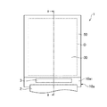
はじめに、本発明の一実施形態(第1の実施形態)に係る有機エレクトロルミネッセンス表示装置1について説明する。図1は本発明の一実施形態に係る有機エレクトロルミネッセンス表示装置1の概略平面図であり、図2は図1に示す有機エレクトロルミネッセンス表示装置1のII−II切断線における概略断面図である。本実施形態に係る有機エレクトロルミネッセンス表示装置1は、素子基板10と、フレキシブル回路基板2と、駆動ドライバ3と、素子基板10上に設けられた有機エレクトロルミネッセンス素子30と、封止膜40と、保護膜50と、を有している。
First, an organic
本実施形態における素子基板10は、例えば基板10aと駆動領域10bから構成されている。基板10aは、例えば矩形の低温ポリシリコン層が形成された基板である。なお、ここでいう「低温ポリシリコン」とは、摂氏600℃以下の条件下で形成されたポリシリコンをいう。
The
基板10aの上面10a1のうち、駆動領域10bが形成されていない領域には、フレキシブル回路基板2が接続され、さらに、駆動ドライバ3が設けられている。駆動ドライバ3は、有機エレクトロルミネッセンス表示装置1の外部からフレキシブル回路基板2を介して画像データを供給されるドライバである。駆動ドライバ3は画像データを供給されることにより、有機エレクトロルミネッセンス素子30に、図示しないデータ線を介して表示データを供給する。
Of the
駆動領域10bは、基板10a上に形成された、図示しないトランジスタが形成された領域である。このトランジスタは有機エレクトロルミネッセンス素子30を駆動するためのトランジスタであり、画素Pごとに基板10a上に設けられている。このトランジスタは、既知の構成を採用することができ、具体的には例えば、図示しないゲート電極やソース・ドレイン電極、層間絶縁膜等によって構成されている。トランジスタの上面は、絶縁体からなるパッシベーション層によって覆われており、その上面は素子基板10(駆動領域10b)の上面10cを構成している。
The
なお、素子基板10の構成はここに挙げた例に限られず、有機エレクトロルミネッセンス素子30を駆動可能で、かつ、その上面10cが平坦で絶縁性を有するものであれば、その他の構成であってもよい。
Note that the configuration of the
有機エレクトロルミネッセンス素子30は、素子基板10上に設けられている。有機エレクトロルミネッセンス素子30は、例えば平面視で素子基板10よりも小さい外周を有する表示領域Dに設けられており、その外側の領域には、例えば光不透過膜からなるブラックマトリクスBMが配置されている。
The
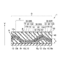
図3は図2に示す有機エレクトロルミネッセンス表示装置1のIII領域の部分拡大図である。このIII領域は、表示領域Dにおける4つの画素Pに対応する領域である。III領域の素子基板10上には、起伏部12と、有機エレクトロルミネッセンス素子30と、封止膜40と、保護膜50とが積層されている。
FIG. 3 is a partial enlarged view of region III of the organic
起伏部12は絶縁体からなり、画素P毎に応じて素子基板上10上に形成されている。起伏部12は一方向に延在しており、図3に示す起伏部12は、その延在方向に直角な切断線で切断された状態を示している。なお、起伏部12の延在方向の長さは、所望の画素Pの大きさに応じて適宜設定すればよい。
The undulating
起伏部12は、断面形状が例えば三角形であり、素子基板10の上面10cに対しての角度が鋭角である複数の斜面を有している。本実施形態における起伏部12は、例えば、上面10cに対しての角度がθgである第1斜面12aと、上面10cに対しての角度がθrである第2斜面12bを有している。
The undulating
この第1斜面12aは、上面10cに対しての角度が90°−θgである第1の方向Aに対して垂直であり、第2斜面12bは、上面10cに対しての角度が90°−θrである第2の方向Bに対して垂直である。また、第2の方向Bは第1の方向Aとは異なる方向を示している。
The first
素子基板10の上面10cに垂直な方向を垂直方向Vとすると、起伏部上部12cが、起伏部12のうち、上面10cからの垂直方向Vの距離(高さh)が最も大きい領域となる。起伏部上部12cの形状は、図3に示すような、全く平面のない峰状の形状のみならず、製造の工程により峰状の形状から誤差の範囲でずれたものも含む。また、起伏部12の断面形状は図3に示すように三角形であることが好ましいが、上辺が下辺よりも小さい台形であってもよい。高さhは例えば10μm〜100μmとすることができるが、画素Pの幅に応じて適宜設定すればよい。
Assuming that the direction perpendicular to the
隣接する起伏部12同士は、互いに間隔を空けて設けられている。素子基板10の上面10cのうち、起伏部12同士間の領域を起伏部間領域13とする。本実施形態における起伏部間領域13は、素子基板10の上面10cのうち、起伏部12に覆われていない領域を示す。
また、第1斜面12a、第2斜面12b及び起伏部間領域13は、それぞれ各画素Pに対応するようにマトリクス状に形成されている。
The
有機エレクトロルミネッセンス素子30は、例えば、緑色に発光する第1発光層17Gを有する第1有機エレクトロルミネッセンス素子30Gと、赤色に発光する第2発光層17Rを有する第2有機エレクトロルミネッセンス素子30Rと、青色に発光する第3発光層17Bを有する第3有機エレクトロルミネッセンス素子30Bと、を有している。なお、第1発光層17G、第2発光層17R及び第3発光層17Bの発光色はここに挙げた例に限られず、その他の色であってもよい。また、第1発光層17G、第2発光層17R及び第3発光層17Bは、それぞれ異なる色で発光するものに限られず、これら3種類のうち2つ、あるいは3種類全てが同じ色で発光するものであってもよい。
The
第1有機エレクトロルミネッセンス素子30Gは第1斜面12a上に形成され、第2有機エレクトロルミネッセンス素子30Rは第2斜面12b上に形成され、第3有機エレクトロルミネッセンス素子30Bは起伏部間領域13上形成されている。
The first organic electroluminescent element 30G is formed on the first
このうち、第1有機エレクトロルミネッセンス素子30Gの構成について説明する。第1有機エレクトロルミネッセンス素子30Gは、例えば、第1下部電極15Gと、第1発光層17Gを含む有機層20と、上部電極19と、を有している。
Among these, the structure of the 1st organic electroluminescent element 30G is demonstrated. The first organic electroluminescence element 30G includes, for example, a first
第1下部電極15Gは、起伏部12の第1斜面12a上に形成されている。第1下部電極15Gは例えばAg等の金属からなるが、その材料はAgに限定されず、その他のものであってもよい。第1下部電極15Gは、駆動領域10bに設けられた図示しないコンタクトホールを介して、図示しないトランジスタに電気的に接続されている。このような構成を有することにより、トランジスタから供給される駆動電流は、第1下部電極15Gを介して第1発光層17Gに注入される。
The first
有機層20は第1下部電極15G上に形成されている。有機層20は、例えば、第1下部電極15G側から順に、ホール輸送層16、第1発光層17G及びホールブロック層18が積層してなる。有機層20の積層構造はここに挙げたものに限られず、少なくとも第1発光層17Gを含むものであれば、その構造は特定されない。
The
ホール輸送層16は、第1下部電極15G上と第1斜面12a上を覆うように形成されている。本実施形態におけるホール輸送層16は第1下部電極15G、第2下部電極15R及び第3下部電極15Bに共通して接触している。第1下部電極15G上に位置するホール輸送層16は、第1下部電極15Gから注入されたホール(正孔)を第1発光層17Gに輸送する機能を有する。
The
本実施形態における第1発光層17Gは、第1下部電極15G上にホール輸送層16を介して形成されている。第1発光層17Gは例えば、ホールと電子とが結合することによって緑色に発光する有機エレクトロルミネッセンス物質から構成されている。なお、第1発光層17Gの発光色は緑色に限られず、白色光を発するものであっても、その他の色の光を発するものであってもよい。
The first
また、第1発光層17G上には、ホールブロック層18が形成されている。ホールブロック層18は、第1下部電極15Gから注入されたホールをブロックする機能を有する。
A
本実施形態における第1有機エレクトロルミネッセンス素子30Gの有機層20上には、第3発光層17Bが形成されていてもよい。第3発光層17Bは例えば、第1発光層17Gと異なる色で発光する発光層である。このような構成であっても、第1発光層17Gと第3発光層17Bとの間にホールブロック層18が形成されているため、第1下部電極15Gから注入されたホールがホールブロック層18においてブロックされる。このため、ホールブロック層18上に形成された第3発光層17Bへのホールの輸送が防がれ、第1発光層17G上の第3発光層17Bが発光することはない。
The third
上部電極19は、有機層20上(第1発光層17G上)に形成されている。なお、本実施形態における第1有機エレクトロルミネッセンス素子30Gの有機層20上には、ホールブロック層18と、第3発光層17Bが形成されているため、上部電極19は第3発光層17B上を覆うように形成されている。
The
上部電極19は複数の有機エレクトロルミネッセンス素子30(第1、第2、第3有機エレクトロルミネッセンス素子30G、30R、30B)の有機層20に共通に接触する、透明な共通電極である。上部電極19は、例えばITO等の透光性及び導電性を有する材料からなる。
The
次いで、第2有機エレクトロルミネッセンス素子30Rの構成について説明する。第2有機エレクトロルミネッセンス素子30Rは、第2下部電極15Rと、第2発光層17Rを含む有機層20と、上部電極19と、を有している。なお、第2有機エレクトロルミネッセンス素子30Rの構成は、第2下部電極15Rが第2斜面12bに形成される点と、第2発光層17Rが例えば赤色に発光する点と、ホールブロック層18が形成されていない点が第1有機エレクトロルミネッセンス素子30Gと異なる。以下、第1有機エレクトロルミネッセンス素子30Gと同様の構成についてはその説明を省略する。
Next, the configuration of the second organic electroluminescence element 30R will be described. The second organic electroluminescent element 30R includes a second
第2下部電極15Rは、起伏部12の第2斜面12b上に形成されている。第2下部電極15R上には、ホール輸送層16と第2発光層17Rが積層してなる有機層20が形成されている。第2発光層17Rは例えば赤色に発光する発光層である。なお、第2発光層17Rの発光色は赤色に限られず、白色光を発するものであっても、その他の色の光を発するものであってもよい。また、有機層20上(第2発光層17R上)には、上部電極19が形成されている。
The second
次いで、第3有機エレクトロルミネッセンス素子30Bの構成について説明する。第3有機エレクトロルミネッセンス素子30Bは、例えば、第3下部電極15Bと、第3発光層17Bを含む有機層20と、上部電極19と、を有している。なお、第3有機エレクトロルミネッセンス素子30Bの構成は、第3下部電極15Bが起伏部間領域13(上面10c)上に形成される点と、第3発光層17Bが例えば青色に発光する点と、ホールブロック層18が形成されていない点が第1有機エレクトロルミネッセンス素子30Gと異なる。以下、第1有機エレクトロルミネッセンス素子30Gと同様の構成についてはその説明を省略する。
Next, the configuration of the third organic electroluminescence element 30B will be described. The third organic electroluminescence element 30B includes, for example, a third
第3下部電極15Bは、起伏部間領域13上に形成されている。第3下部電極15B上には、ホール輸送層16と第3発光層17Bが積層してなる有機層20が形成されている。第3発光層17Bは例えば青色に発光する発光層である。なお、第3発光層17Bの発光色は青色に限られず、白色光を発するものであっても、その他の色の光を発するものであってもよい。また、有機層20上(第3発光層17B上)には、上部電極19が形成されている。
The third
各有機エレクトロルミネッセンス素子30(第1、第2、第3有機エレクトロルミネッセンス素子30G、30R、30B)上は封止膜40によって覆われている。封止膜40は、例えば、SiNや、SiO、SiON、樹脂などからなり、これらの材料からなる単層膜であっても、積層構造であってもよい。
Each organic electroluminescence element 30 (first, second, and third organic electroluminescence elements 30G, 30R, and 30B) is covered with a sealing
保護膜50は、封止膜40上に配置されている。保護膜50は封止膜40の表面を保護するものであれば、その構成や材料は限られず、既知のものを用いてもよい。また、保護膜50に代えて、例えばガラスや石英、プラスチックなどの透光性材料からなる基板を封止膜40上に配置してもよい。
The
本実施形態における有機エレクトロルミネッセンス表示装置1は、起伏部12の第1斜面12a上、第2斜面12b上及び起伏部間領域13上にそれぞれ、有機エレクトロルミネッセンス素子30(第1、第2、第3有機エレクトロルミネッセンス素子30G、30R、30B)が形成されている。このため、このような構成を有しない有機エレクトロルミネッセンス表示装置と比べ、有機エレクトロルミネッセンス素子30が設けられる領域の面積が広くなり、輝度が向上する。また、一定の輝度を得るための発光層における単位面積の電流密度を低減できるため、有機エレクトロルミネッセンス表示装置1の寿命が向上する。
In the organic
また、各画素Pに応じて設けられた起伏部12の第1斜面12a上と第2斜面12b上及び起伏部間領域13上にそれぞれ有機エレクトロルミネッセンス素子30が形成されていることにより、このような構成を有さない有機エレクトロルミネッセンス表示装置と比べ、各画素P間における有機エレクトロルミネッセンス素子30の位置ずれが生じにくい。
In addition, since the
また、第1斜面12aと第2斜面12bに形成された有機エレクトロルミネッセンス素子30が発光することにより、第1斜面12a及び第2斜面12bから斜め方向に発出された光は、有機エレクトロルミネッセンス表示装置1の正面方向(垂直方向V)に進む。このため、有機エレクトロルミネッセンス素子30の有機層20を構成する層、封止膜40及び保護膜50の少なくともいずれか一つが、輝度のピークが膜面に対して斜め方向となる膜構成を有することにより、有機エレクトロルミネッセンス表示装置1の正面方向の輝度を向上させることができる。
Further, when the
さらに、起伏部12の第1斜面12aと上面10cの成す角度θgと、第2斜面12b斜面12bと上面10cの成す角度θrは鋭角であるため、起伏部12のアスペクト比、すなわち起伏部12の底面の幅に対する高さhの比率が小さく抑えられる。このため、壁部を有する有機エレクトロルミネッセンス表示装置と比べ、画素Pを小さくしても、起伏部12の強度低下が抑えられる。このため、起伏部12の破損が防がれ、有機エレクトロルミネッセンス表示装置1に表示される画像の画質低下を抑えることができる。
Furthermore, since the angle θ g formed between the first
また、本実施形態における有機エレクトロルミネッセンス表示装置1は、第1斜面12a上に第1下部電極15Gと第1発光層17Gが形成され、第2斜面12b上に第2下部電極15Rと第2発光層17Rが形成され、起伏部間領域13上に第3下部電極15Bと第3発光層17Bが形成され、第1発光層17G、第2発光層17R及び第3発光層17Bが、それぞれ異なる色で発光することにより、このような構成を有さない有機エレクトロルミネッセンス表示装置と比べ、画素Pの微細化と、混色の防止を実現することができる。このため、有機エレクトロルミネッセンス表示装置1に表示される画像の画質を向上させることができる。
In the organic
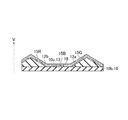
次いで、第2の実施形態に係る有機エレクトロルミネッセンス表示装置1について説明する。図4は第2の実施形態に係る有機エレクトロルミネッセンス表示装置1のIII領域に対応する領域の部分拡大図である。第2の実施形態に係る有機エレクトロルミネッセンス表示装置1は、バンク14を有する点が、第1の実施形態に係る有機エレクトロルミネッセンス表示装置1と異なっている。以下、バンク14に関する構成について説明し、第1の実施形態に係る有機エレクトロルミネッセンス表示装置1と同様の構成についてはその説明を省略する。
Next, the organic
第2の実施形態に係る有機エレクトロルミネッセンス表示装置1は、第1斜面12aと素子基板10の上面10cの境界10c1に形成された、垂直方向Vに突出するバンク14(第1バンク14a)と、第2斜面12bと上面10cの境界10c2に形成された、垂直方向Vに突出するバンク14(第2バンク14b)と、起伏部上部12cに形成された、垂直方向Vに突出するバンク14(第3バンク14c)と、を有している。
The organic
バンク14の垂直方向Vの高さは、バンク14の上端14tが上部電極19の上面より下に位置すればよい。また、上端14tの位置は、上部電極19と有機層20の境界に近いほど好ましい。また、バンク14の幅は、画素Pの大きさや起伏部上部12cの幅に応じて適宜設定すればよい。
The height of the bank 14 in the vertical direction V may be such that the
本実施形態における有機エレクトロルミネッセンス表示装置1は、上記構成を有することにより、隣接する各画素P同士の境界である境界10c1、10c2及び起伏部上部12cにおいて、異なる色の発光層が重なることが防がれる。このため、隣接する画素P同士の混色を防ぐことができ、有機エレクトロルミネッセンス表示装置1に表示される画像の画質を向上させることができる。
Since the organic
次いで、本発明の一実施形態に係る有機エレクトロルミネッセンス表示装置1の製造方法について図面を用いて説明する。図5乃至10は本発明の一実施形態に係る態有機エレクトロルミネッセンス表示装置の製造方法を示す、III領域に対応する領域の部分拡大図である。
Next, a method for manufacturing the organic
本実施形態における有機エレクトロルミネッセンス表示装置1の製造方法は、素子基板10を形成する工程と、素子基板10上に、素子基板10の上面10cに対しての角度が鋭角である複数の斜面(第1斜面12a、第2斜面12b)を有する複数の起伏部12を、互いに間隔を空けて形成する工程と、有機エレクトロルミネッセンス素子30を、各斜面(第1斜面12a、第2斜面12b)上、及び、素子基板10の上面10cのうち起伏部12同士の間の領域である起伏部間領域13上にそれぞれ形成する工程と、を有する。
The manufacturing method of the organic
初めに、素子基板10を形成する。まず、例えば矩形の低温ポリシリコン基板である基板10aを用意する。次いで、基板10a上に、図示しないトランジスタを有する、上面10cが平坦な駆動領域10bを形成する。これにより、素子基板10が形成される。
First, the
次いで、図5に示すように、例えばフォトリソグラフィにより、上面10cに対しての角度が鋭角である第1斜面12aと、第1斜面12aとは異なる方向に面する第2斜面12bとを有する、絶縁体からなる起伏部12を、画素Pに応じて素子基板10上に形成する。この起伏部12を形成する方法はフォトリソグラフィに限られず、素子基板10の上面10cに対しての角度が鋭角である複数の斜面を有する起伏部12を形成することができるものであれば、ナノインプリントなどその他の方法であってもよい。
Next, as shown in FIG. 5, for example, by photolithography, the first
なお、起伏部12は、図5に示すように、その断面形状が三角形状となるように形成されることが好ましいが、上辺が下辺よりも小さい台形形状となるように形成してもよい。また、起伏部上部12cのV方向の高さは例えば10μm〜100μmとすることができるが、画素Pの幅に応じて適宜設定すればよい。
As shown in FIG. 5, the undulating
また、第1斜面12aと素子基板10の上面10cの境界10c1、第2斜面12bと上面10cの境界10c2及び起伏部上部12cに、図示しないバンクを形成してもよい。バンクの垂直方向Vの高さは、後述する有機エレクトロルミネッセンス素子30のV方向の高さに応じて適宜設定すればよい。また、バンクの幅は、画素Pの大きさや起伏部上部12cの幅に応じて適宜設定すればよい。
Banks (not shown) may be formed on the
次いで、有機エレクトロルミネッセンス素子30を、素子基板10の上面10cのうち起伏部12同士の間の領域である各斜面(第1斜面12a、第2斜面12b)上と起伏部間領域13上とにそれぞれ形成する。有機エレクトロルミネッセンス素子30を形成する工程は、下部電極(第1下部電極15G、第2下部電極15R、第3下部電極15B)を形成する工程と、有機層20を形成する工程と、上部電極19を形成する工程と、を有する。
Next, the
まず、図6に示すように、第1斜面12a、第2斜面12b及び起伏部間領域13上にそれぞれ下部電極を形成する。この下部電極のうち、第1斜面12a上に形成したものを第1下部電極15G、第2斜面12b上に形成したものを第2下部電極15R、起伏部間領域13上に形成したものを第3下部電極15Bとする。これら第1下部電極15G、第2下部電極15R及び第3下部電極15Bは、駆動領域10b内の図示しないトランジスタに電気的に接続される。
First, as shown in FIG. 6, lower electrodes are formed on the
次いで、有機層20を形成する。有機層20を形成する工程は更に、ホール輸送層16を形成する工程と、第1の蒸着方向Gからの蒸着により、第1下部電極15G上に第1発光層17Gとホールブロック層18を順に形成する第1蒸着工程と、第2の蒸着方向Rからの蒸着により、第2下部電極15R上に第2発光層17Rを形成する第2蒸着工程と、第3の蒸着方向Bからの蒸着により、第3下部電極15B上に第3発光層17Bを形成する第3蒸着工程と、を有している。
Next, the
まず、図7に示すように、第1斜面12a、第2斜面12b及び起伏部間領域13上、及び、第1下部電極15G、第2下部電極15R、第3下部電極15B上を覆うように、ホール輸送層16を形成する。
First, as shown in FIG. 7, the
次いで、第1蒸着工程について説明する。まず、図8に示すように、第1の蒸着方向Gからの斜方蒸着により、第1下部電極15G上の領域に第1発光層17Gとホールブロック層18を順に形成する。この第1の蒸着方向Gと垂直方向Vの成す角度を角度θ1とし、起伏部12の延在方向に垂直な方向Wに対する第1斜面12aの幅をWG、第2斜面12bの幅をWR、起伏部間領域13の幅をWB、起伏部12の高さをhとすると、角度θ1をtan−1((WR+WB)/h)以上に設定することにより、第2斜面12b上のホール輸送層16及び起伏部間領域13上のホール輸送層16には被蒸着物が付着しない。これは、第2斜面12b上と起伏部間領域13に対応する領域への斜方蒸着が、第1斜面12aによって遮られるためである。
Next, the first vapor deposition step will be described. First, as shown in FIG. 8, a first
このように第1の蒸着方向Gの角度θ1を設定することにより、第1発光層17Gとホールブロック層18が、ホール輸送層16上の、第1斜面12aに対応する領域(第1下部電極15G上)に選択的に形成される。
By setting the angle θ 1 of the first vapor deposition direction G in this way, the first
次いで、第2蒸着工程について説明する。まず図9に示すように、第2の蒸着方向Rからの斜方蒸着により、第2下部電極15R上の領域に、第1発光層17Gとは異なる色で発光する第2発光層17Rを形成する。この蒸着方向と垂直方向Vの成す角度を角度θ2とすると、角度θ2をtan−1((WG+WB)/h)以上に設定することにより、第1斜面12a上のホール輸送層16及び起伏部間領域13上のホール輸送層16には被蒸着物が付着しない。これは、第1斜面12a上と起伏部間領域13に対応する領域への斜方蒸着が、第2斜面12bによって遮られるためである。
Next, the second vapor deposition step will be described. First, as shown in FIG. 9, the second
このように第2の蒸着方向Rの角度θ2を設定することにより、第2発光層17Rは、ホール輸送層16上の、第2斜面12bに対応する領域(第2下部電極15R上)に選択的に形成される。
By setting the angle θ 2 of the second vapor deposition direction R in this way, the second
次いで、第3蒸着工程について説明する。まず、図10に示すように、第3の蒸着方向Bからの斜方蒸着により、第3下部電極15B上の領域に、第1発光層17G及び第2発光層17Rとは異なる色で発光する第3発光層17Bを形成する。この第3の蒸着方向Bと垂直方向Vの成す角度を角度θ3とすると、角度θ3をtan−1(WR/h)以上、かつ、tan−1(WR+WB/h)以下に設定することにより、第2斜面12b上の第2発光層17Rには被蒸着物が付着しない。これは、第2斜面12b上に対応する領域への斜方蒸着が、第1斜面12aによって遮られるためである。
Next, the third vapor deposition step will be described. First, as shown in FIG. 10, light is emitted in a color different from that of the first
このように第3の蒸着方向Bの角度θ3を設定することにより、第3発光層17Bは、ホール輸送層16上の、起伏部間領域13に対応する領域(第3下部電極15B上)に選択的に形成される。
By setting the angle θ 3 in the third vapor deposition direction B in this way, the third
なお、第3の蒸着方向Bが垂直方向Vと成す角度θ3を、第1の蒸着方向Gが垂直方向Vと成す角度θ1よりも小さくすることにより、第1斜面12a上に対応する領域にも被蒸着物が付着する。しかし、第1発光層17G上はホールブロック層18により覆われているため、第1下部電極15Gから注入されるホールはホールブロック層18においてブロックされる。このため、有機エレクトロルミネッセンス素子30を駆動しても、ホールブロック層18上の第3発光層17Bへのホールの輸送が防がれ、第1発光層17G上の第3発光層17Bが発光することはない。
Note that by a third deposition direction B is the angle theta 3 formed by the vertical direction V, the first deposition direction G is smaller than the angle theta 1 which forms a vertical direction V, the region corresponding to the first
次いで、有機層20上を覆うように上部電極19を形成する。以上により、図3に示す有機エレクトロルミネッセンス素子30が形成される。その後、各有機エレクトロルミネッセンス素子30上を覆う封止膜40を形成し、封止膜40上を覆う保護膜50を形成することにより、図3に示す有機エレクトロルミネッセンス表示装置1が製造される。
Next, the
本実施形態における有機エレクトロルミネッセンス表示装置1の製造方法は、第1の蒸着方向Gからの蒸着により第1斜面12a上に第1発光層17Gとホールブロック層18を形成し、第2の蒸着方向Rからの蒸着により第2斜面12b上に第2発光層17Rを形成し、第2の蒸着方向Rからの蒸着により第2斜面12b上に第2発光層17Rを形成し、角度θ3を角度θ1よりも小さくすることにより、画素P間に壁部やブラックマトリクスを設けることなく、各画素Pに対応する領域に、異なる色で発光する複数種類の発光層を塗り分けることができる。このため、本構成を有さない有機エレクトロルミネッセンス表示装置1の製造方法と比べ、画素Pを微細化しても、発光層を正確に塗り分けることができる。これにより、高画質の画像を表示可能な有機エレクトロルミネッセンス表示装置1を提供することができる。
In the manufacturing method of the organic
また、本実施形態における製造方法は、画素P間に壁部を設ける有機エレクトロルミネッセンス表示装置の製造方法と比べ、高輝度で、かつ、寿命の長い有機エレクトロルミネッセンス表示装置1を提供することができる。また、本実施形態における製造方法は、画素Pの領域に応じて、上面10cに対しての角度が鋭角である斜面を有する起伏部12を形成するため、画素Pを微細化しても、起伏部12の強度低下が抑えられる。このため、起伏部12の破損と、それによる画質低下を抑えることが可能な有機エレクトロルミネッセンス表示装置1を提供することができる。
In addition, the manufacturing method in the present embodiment can provide the organic
以上、本発明の実施形態を説明してきたが、本発明は、上述した実施形態には限られない。例えば、上述した実施形態で説明した構成は、実質的に同一の構成、同一の作用効果を奏する構成、又は同一の目的を達成することができる構成により置き換えてもよい。 As mentioned above, although embodiment of this invention was described, this invention is not restricted to embodiment mentioned above. For example, the configuration described in the above-described embodiment may be replaced by a configuration that has substantially the same configuration, a configuration that exhibits the same operational effects, or a configuration that can achieve the same purpose.
例えば、第1斜面12aと第1下部電極15Gの間、第2斜面12bと第2下部電極15Rの間、起伏部間領域13と第3下部電極15Bの間に、図示しない反射膜が設けられていてもよい。反射膜は、有機エレクトロルミネッセンス素子30から発出した光を封止膜40側へ向けて反射するために設けられる。このような反射膜は、光反射率が高いほど好ましく、例えばアルミニウムや銀等からなる金属膜を用いることができる。
For example, a reflective film (not shown) is provided between the
1 有機エレクトロルミネッセンス表示装置、2 フレキシブル回路基板、3 駆動ドライバ、10 素子基板、10a 基板、10b 駆動領域、10c 上面、10c1,10c2 境界、12 起伏部、12a 第1斜面、12b 第2斜面、12c 起伏部上部、13 起伏部間領域、14 バンク、14a 第1バンク、14b 第2バンク、14c 第3バンク、15G 第1下部電極、15R 第2下部電極、15B 第3下部電極、16 ホール輸送層、17G 第1発光層、17R 第2発光層、17B 第3発光層、18 ホールブロック層、19 上部電極、20 有機層、30 有機エレクトロルミネッセンス素子、30G 第1有機エレクトロルミネッセンス素子、30R 第2有機エレクトロルミネッセンス素子、30B 第3有機エレクトロルミネッセンス素子、40 封止膜、50 保護膜、A 第1の方向、B 第2の方向、G 第1の蒸着方向、R 第2の蒸着方向、B 第3の蒸着方向、h 高さ、V 垂直方向、θg,θr 角度、θ1,θ2,θ3 角度、WG,WR,WB 幅。
1 the organic electroluminescent display device, 2 a flexible circuit board, 3 driver, 10 device substrate, 10a substrate, 10b drive region, 10c upper surface, 10c 1, 10c 2 boundary, 12 undulations, 12a first slope, 12b second
Claims (12)
前記素子基板上に形成された、前記素子基板の上面に対して垂直方向の高さを有する起伏部と、
有機エレクトロルミネッセンス素子と、を有し、
前記起伏部が、前記素子基板の上面に対しての角度が鋭角である複数の斜面を有し、
前記有機エレクトロルミネッセンス素子が、前記素子基板の上面のうち前記起伏部同士の間の領域である起伏部間領域上と各前記斜面上にそれぞれ形成され、
前記複数の斜面が、
第1の方向に対して垂直である第1斜面と、
前記第1の方向とは異なる方向である第2の方向に対して垂直である第2斜面と、を有し、
前記有機エレクトロルミネッセンス素子が、
前記第1斜面上に形成された第1下部電極と前記第1下部電極上に形成された第1発光層と、
前記第2斜面上に形成された第2下部電極と前記第2下部電極上に形成された第2発光層と、
前記起伏部間領域上に形成された第3下部電極と前記第3下部電極上に形成された第3発光層と、
を有し、
前記第1発光層、前記第2発光層及び前記第3発光層がそれぞれ異なる色で発光する、
ことを特徴とする有機エレクトロルミネッセンス表示装置。 An element substrate;
An undulation formed on the element substrate and having a height in a direction perpendicular to the upper surface of the element substrate;
An organic electroluminescence element,
The undulating portion has a plurality of inclined surfaces with an acute angle with respect to the upper surface of the element substrate;
The organic electroluminescence element is formed on each of the slopes on the region between the undulations that is a region between the undulations on the upper surface of the element substrate, respectively.
The plurality of slopes are
A first slope that is perpendicular to the first direction;
A second slope that is perpendicular to a second direction that is different from the first direction;
The organic electroluminescence element is
A first lower electrode formed on the first slope and a first light emitting layer formed on the first lower electrode;
A second lower electrode formed on the second slope and a second light emitting layer formed on the second lower electrode;
A third lower electrode formed on the region between the undulations and a third light emitting layer formed on the third lower electrode;
Have
The first light-emitting layer, the second light-emitting layer and the third light-emitting layer emit light in different colors,
An organic electroluminescence display device.
前記第1斜面と前記素子基板の上面の境界に形成された、前記垂直方向に突出する第1バンクと、
前記第2斜面と前記素子基板の上面の境界に形成された、前記垂直方向に突出する第2バンクと、
前記第1斜面と前記第2斜面との間に位置する、前記素子基板の上面からの前記垂直方向の距離が前記起伏部のうち最も大きい領域である起伏部上部に形成された、前記垂直方向に突出する第3バンクと、
を有することを特徴とする有機エレクトロルミネッセンス表示装置。 The organic electroluminescence display device according to claim 1 ,
A first bank protruding in the vertical direction and formed at a boundary between the first slope and the upper surface of the element substrate;
A second bank protruding in the vertical direction and formed at a boundary between the second slope and the upper surface of the element substrate;
The vertical direction, which is formed between the first slope and the second slope, is formed on an upper portion of the undulating portion, which is the largest region of the undulating portion, in the vertical direction from the upper surface of the element substrate. A third bank protruding into
An organic electroluminescence display device comprising:
有機エレクトロルミネッセンス素子を、前記素子基板の上面のうち前記起伏部同士の間の領域である起伏部間領域上と各前記斜面上とにそれぞれ形成する工程と、
を有し、
前記起伏部を形成する工程において、
第1斜面と前記第1斜面とは異なる方向に面する第2斜面とを形成し、
前記有機エレクトロルミネッセンス素子を形成する工程が、
前記第1斜面、前記第2斜面及び前記起伏部間領域上にそれぞれ第1下部電極、第2下部電極及び第3下部電極を形成する工程と、
第1の蒸着方向からの蒸着により、前記第1下部電極上に第1発光層とホールブロック層を順に形成する第1蒸着工程と、
第2の蒸着方向からの蒸着により、前記第2下部電極上に第2発光層を形成する第2蒸着工程と、
第3の蒸着方向からの蒸着により、前記第3下部電極上に第3発光層を形成する第3蒸着工程と、
前記第1発光層、前記第2発光層及び前記第3発光層上に上部電極を形成する工程と、を有し、
前記第3の蒸着方向が前記素子基板の垂直方向と成す角度が、前記第1の蒸着方向が前記垂直方向と成す角度よりも小さく、
前記第1発光層と前記第2発光層と前記第3発光層とが、それぞれ異なる色で発光することを特徴とする有機エレクトロルミネッセンス表示装置の製造方法。 On the element substrate, forming undulations having a plurality of inclined surfaces with an acute angle with respect to the upper surface of the element substrate, spaced apart from each other;
Forming an organic electroluminescent element on the region between the undulating portions, which is a region between the undulating portions of the upper surface of the element substrate, and on each of the inclined surfaces;
Have
In the step of forming the undulations,
Forming a first slope and a second slope facing in a different direction from the first slope;
Forming the organic electroluminescence element,
Forming a first lower electrode, a second lower electrode, and a third lower electrode on the first slope, the second slope, and the region between the undulations, respectively;
A first vapor deposition step of sequentially forming a first light emitting layer and a hole blocking layer on the first lower electrode by vapor deposition from a first vapor deposition direction;
A second vapor deposition step of forming a second light emitting layer on the second lower electrode by vapor deposition from a second vapor deposition direction;
A third vapor deposition step of forming a third light emitting layer on the third lower electrode by vapor deposition from a third vapor deposition direction;
Forming an upper electrode on the first light emitting layer, the second light emitting layer, and the third light emitting layer,
The angle formed by the third deposition direction with the vertical direction of the element substrate is smaller than the angle formed by the first deposition direction with the vertical direction.
The method of manufacturing an organic electroluminescence display device, wherein the first light emitting layer, the second light emitting layer, and the third light emitting layer emit light in different colors.
前記基板上に形成された第1起伏部と、
前記基板上に形成され、前記第1起伏部に隣接する第2起伏部と、
前記第1起伏部と前記第2起伏部との間に位置する起伏部間領域と、
前記第1起伏部が有する複数の斜面のうち、前記起伏部間領域の側に位置する第1斜面と、
前記第2起伏部が有する複数の斜面のうち、前記起伏部間領域の側に位置する第2斜面と、
前記第1斜面上に形成された第1下部電極と、
前記第2斜面上に形成された第2下部電極と、
前記起伏部間領域上に形成された第3下部電極と、
前記第1下部電極上を覆う第1発光層と、
前記第2下部電極上を覆う第2発光層と、
前記第3下部電極上を覆う第3発光層と、
少なくとも前記第1発光層上を覆う上部電極と、を有することを特徴とする有機エレクトロルミネッセンス表示装置。 A substrate,
A first undulation formed on the substrate;
A second undulation formed on the substrate and adjacent to the first undulation;
A region between undulations located between the first undulations and the second undulations;
Of the plurality of slopes of the first undulation portion, a first slope located on the side of the region between the undulation portions,
Of the plurality of slopes of the second undulation part, a second slope located on the side of the region between the undulation parts,
A first lower electrode formed on the first slope;
A second lower electrode formed on the second slope;
A third lower electrode formed on the region between the undulations;
A first light emitting layer covering the first lower electrode;
A second light emitting layer covering the second lower electrode;
A third light emitting layer covering the third lower electrode;
An organic electroluminescence display device comprising: an upper electrode covering at least the first light emitting layer.
前記第1発光層上に、前記第1発光層を覆うブロック層が形成され、
前記第3の発光層は、前記第1下部電極上において、前記起伏部間領域上と前記第1斜面上とに跨って形成され、
前記ブロック層は、前記第1発光層と前記第3発光層との間に位置することを特徴とする有機エレクトロルミネッセンス表示装置。 The organic electroluminescence display device according to claim 4 ,
A block layer that covers the first light emitting layer is formed on the first light emitting layer,
The third light emitting layer is formed on the first lower electrode so as to straddle the region between the undulations and the first slope.
The organic electroluminescence display device, wherein the block layer is located between the first light emitting layer and the third light emitting layer.
前記第1下部電極上と前記第2下部電極上と前記第3下部極上とを覆い、且つ前記第1斜面上と前記第2斜面上と前記起伏部間領域上とに跨って位置するホール輸送層を備え、
前記ブロック層は、前記第1下部電極から注入されたホールをブロックするホールブロック層であることを特徴とする有機エレクトロルミネッセンス表示装置。 The organic electroluminescence display device according to claim 5 ,
Hole transport that covers the first lower electrode, the second lower electrode, and the third lower pole, and that is located over the first slope, the second slope, and the region between the undulations. With layers,
The organic electroluminescence display device, wherein the block layer is a hole block layer that blocks holes injected from the first lower electrode.
前記第1下部電極上と前記第2下部電極上と前記第3下部極上とを覆い、前記第1斜面上と前記第2斜面上と前記起伏部間領域上とに跨って位置するホール輸送層が形成されていることを特徴とする有機エレクトロルミネッセンス表示装置。 The organic electroluminescence display device according to claim 4 ,
A hole transport layer that covers the first lower electrode, the second lower electrode, and the third lower pole, and is located across the first slope, the second slope, and the region between the undulating portions. An organic electroluminescence display device characterized in that is formed.
前記上部電極は、記第1発光層上と前記第2発光層上と前記第3発光層上とを覆い、前記第1斜面上と前記第2斜面上と前記起伏部間領域上とに跨って位置することを特徴とする有機エレクトロルミネッセンス表示装置。 The organic electroluminescence display device according to any one of claims 4 to 7 ,
The upper electrode covers the first light emitting layer, the second light emitting layer, and the third light emitting layer, and straddles the first inclined surface, the second inclined surface, and the region between the undulating portions. An organic electroluminescence display device characterized by being located.
前記第1起伏部及び前記第2起伏部の下層には、絶縁膜が配置され、
前記第1起伏部と重なる領域における前記絶縁膜の上面と前記第1斜面とがなす第1の角、及び前記第2起伏部と重なる領域における前記絶縁膜の上面と前記第2斜面とがなす第2の角が鋭角であることを特徴とする有機エレクトロルミネッセンス表示装置。 The organic electroluminescence display device according to any one of claims 4 to 8 ,
An insulating film is disposed under the first undulation and the second undulation,
A first angle formed by the upper surface of the insulating film and the first inclined surface in a region overlapping the first undulating portion, and an upper surface of the insulating film and the second inclined surface formed in a region overlapping the second undulating portion. An organic electroluminescence display device, wherein the second corner is an acute angle.
前記起伏部間領域の前記第1斜面の側には、前記基板とは反対側に突出する第1突出部が形成され、
前記起伏部間領域の前記第2斜面の側には、前記基板とは反対側に突出する第2突出部が形成され、
前記第1斜面の前記起伏部間領域とは反対側の端部には、前記基板とは反対側に突出する第3突出部が形成されていることを特徴とする有機エレクトロルミネッセンス表示装置。 The organic electroluminescence display device according to any one of claims 4 to 9 ,
On the side of the first inclined surface of the region between the undulations, a first protrusion that protrudes on the opposite side of the substrate is formed,
On the side of the second inclined surface in the region between the undulations, a second protrusion that protrudes on the opposite side of the substrate is formed,
An organic electroluminescence display device, wherein a third projecting portion projecting to the side opposite to the substrate is formed at an end of the first slope opposite to the region between the undulating portions.
前記第1起伏部は、前記第1斜面とは異なる第3斜面を有し、
前記第3斜面は、前記第1斜面の前記端部と接し、
前記第3斜面には、第4下部電極と第4発光層とが形成され、
前記第3突出部は、前記第1発光層と前記第4発光層との間に位置していることを特徴とする有機エレクトロルミネッセンス表示装置。 The organic electroluminescence display device according to claim 10 ,
The first undulation has a third slope different from the first slope,
The third slope is in contact with the end of the first slope;
A fourth lower electrode and a fourth light emitting layer are formed on the third slope,
The organic electroluminescence display device, wherein the third protrusion is positioned between the first light emitting layer and the fourth light emitting layer.
前記上部電極は、前記第1突出部と前記第2突出部と前記第3突出部とを覆っていることを特徴とする有機エレクトロルミネッセンス表示装置。 The organic electroluminescence display device according to claim 10 or 11 ,
The organic electroluminescence display device, wherein the upper electrode covers the first protrusion, the second protrusion, and the third protrusion.
Priority Applications (1)
| Application Number | Priority Date | Filing Date | Title |
|---|---|---|---|
| JP2012254123A JP5980102B2 (en) | 2012-11-20 | 2012-11-20 | ORGANIC ELECTROLUMINESCENT DISPLAY DEVICE AND METHOD FOR PRODUCING ORGANIC ELECTROLUMINESCENT DISPLAY DEVICE |
Applications Claiming Priority (1)
| Application Number | Priority Date | Filing Date | Title |
|---|---|---|---|
| JP2012254123A JP5980102B2 (en) | 2012-11-20 | 2012-11-20 | ORGANIC ELECTROLUMINESCENT DISPLAY DEVICE AND METHOD FOR PRODUCING ORGANIC ELECTROLUMINESCENT DISPLAY DEVICE |
Publications (3)
| Publication Number | Publication Date |
|---|---|
| JP2014102976A JP2014102976A (en) | 2014-06-05 |
| JP2014102976A5 JP2014102976A5 (en) | 2015-04-30 |
| JP5980102B2 true JP5980102B2 (en) | 2016-08-31 |
Family
ID=51025325
Family Applications (1)
| Application Number | Title | Priority Date | Filing Date |
|---|---|---|---|
| JP2012254123A Expired - Fee Related JP5980102B2 (en) | 2012-11-20 | 2012-11-20 | ORGANIC ELECTROLUMINESCENT DISPLAY DEVICE AND METHOD FOR PRODUCING ORGANIC ELECTROLUMINESCENT DISPLAY DEVICE |
Country Status (1)
| Country | Link |
|---|---|
| JP (1) | JP5980102B2 (en) |
Families Citing this family (1)
| Publication number | Priority date | Publication date | Assignee | Title |
|---|---|---|---|---|
| WO2019216196A1 (en) * | 2018-05-08 | 2019-11-14 | ソニーセミコンダクタソリューションズ株式会社 | Display device, method for producing display device, and electronic device |
Family Cites Families (9)
| Publication number | Priority date | Publication date | Assignee | Title |
|---|---|---|---|---|
| JP3785710B2 (en) * | 1996-12-24 | 2006-06-14 | 株式会社デンソー | EL display device |
| JP2001085167A (en) * | 1999-09-20 | 2001-03-30 | Denso Corp | Organic el element and its manufacturing method |
| JP3943900B2 (en) * | 2000-11-09 | 2007-07-11 | 株式会社東芝 | Self-luminous display device |
| JP2003045670A (en) * | 2001-07-30 | 2003-02-14 | Toyota Industries Corp | Organic el display panel and its manufacturing method |
| CN1672469A (en) * | 2002-07-23 | 2005-09-21 | 皇家飞利浦电子股份有限公司 | Electroluminescent display, electronic device comprising such a display and method of manufacturing an electroluminescent display |
| JP2005222734A (en) * | 2004-02-03 | 2005-08-18 | Seiko Epson Corp | Electrooptical device, manufacturing method thereof, and electronic equipment |
| KR101326284B1 (en) * | 2004-09-13 | 2013-11-11 | 가부시키가이샤 한도오따이 에네루기 켄큐쇼 | Lighting Device |
| EP2175504A4 (en) * | 2007-07-31 | 2012-08-22 | Sumitomo Chemical Co | Organic electroluminescence element and method for manufacturing the same |
| JP2009058897A (en) * | 2007-09-03 | 2009-03-19 | Hitachi Displays Ltd | Display device |
-
2012
- 2012-11-20 JP JP2012254123A patent/JP5980102B2/en not_active Expired - Fee Related
Also Published As
| Publication number | Publication date |
|---|---|
| JP2014102976A (en) | 2014-06-05 |
Similar Documents
| Publication | Publication Date | Title |
|---|---|---|
| US9608045B2 (en) | Display device | |
| KR101452768B1 (en) | Display device using semiconductor light emitting device and method of fabricating the same | |
| KR101820197B1 (en) | Thin film transistor array substrate and fabrication method of the same | |
| JP6190709B2 (en) | Organic electroluminescence display device | |
| TWI682378B (en) | Micro-led display panel | |
| JP2018081815A (en) | Display device | |
| JP6521610B2 (en) | Image display device | |
| KR102151609B1 (en) | Display apparatus and manufacturing method of the same | |
| TWI624093B (en) | White light-emitting device, white light-emitting panel including the same, method of manufacturing white light-emitting panel, and display apparatus including white light-emitting device | |
| US20140319475A1 (en) | Organic light emitting diode display and manufacturing method thereof | |
| US10504978B2 (en) | Electroluminescent display device | |
| US11018200B2 (en) | Display device having a white emitting area | |
| JP2018018822A (en) | Display device | |
| JP2016167400A (en) | Display device and manufacturing method for the same | |
| KR20180128387A (en) | Display substrate, display device, and method | |
| WO2016043255A1 (en) | Electroluminescence device, electronic device, and method for manufacturing electroluminescence device | |
| KR101972306B1 (en) | Organic light emitting display device | |
| KR20130010068A (en) | El display panel, el display device provided with el display panel, organic el display device, and method for manufacturing el display panel | |
| JP2018006232A (en) | Display device and manufacturing method thereof | |
| JP2015015114A (en) | Organic electroluminescent display device | |
| WO2013099744A1 (en) | Display device | |
| JP2015149231A (en) | organic EL display device | |
| JP2019012684A (en) | OLED display device and manufacturing method thereof | |
| KR102166004B1 (en) | Organic Light Emitting Display Device and Method of manufacturing the same | |
| JP5980102B2 (en) | ORGANIC ELECTROLUMINESCENT DISPLAY DEVICE AND METHOD FOR PRODUCING ORGANIC ELECTROLUMINESCENT DISPLAY DEVICE |
Legal Events
| Date | Code | Title | Description |
|---|---|---|---|
| A521 | Request for written amendment filed |
Free format text: JAPANESE INTERMEDIATE CODE: A523 Effective date: 20150311 |
|
| A621 | Written request for application examination |
Free format text: JAPANESE INTERMEDIATE CODE: A621 Effective date: 20150311 |
|
| A977 | Report on retrieval |
Free format text: JAPANESE INTERMEDIATE CODE: A971007 Effective date: 20160112 |
|
| A131 | Notification of reasons for refusal |
Free format text: JAPANESE INTERMEDIATE CODE: A131 Effective date: 20160202 |
|
| A521 | Request for written amendment filed |
Free format text: JAPANESE INTERMEDIATE CODE: A523 Effective date: 20160225 |
|
| TRDD | Decision of grant or rejection written | ||
| A01 | Written decision to grant a patent or to grant a registration (utility model) |
Free format text: JAPANESE INTERMEDIATE CODE: A01 Effective date: 20160719 |
|
| A61 | First payment of annual fees (during grant procedure) |
Free format text: JAPANESE INTERMEDIATE CODE: A61 Effective date: 20160726 |
|
| R150 | Certificate of patent or registration of utility model |
Ref document number: 5980102 Country of ref document: JP Free format text: JAPANESE INTERMEDIATE CODE: R150 |
|
| R250 | Receipt of annual fees |
Free format text: JAPANESE INTERMEDIATE CODE: R250 |
|
| R250 | Receipt of annual fees |
Free format text: JAPANESE INTERMEDIATE CODE: R250 |
|
| R250 | Receipt of annual fees |
Free format text: JAPANESE INTERMEDIATE CODE: R250 |
|
| R250 | Receipt of annual fees |
Free format text: JAPANESE INTERMEDIATE CODE: R250 |
|
| LAPS | Cancellation because of no payment of annual fees |