EP2169093A1 - Metal material for electrical electronic component - Google Patents
Metal material for electrical electronic component Download PDFInfo
- Publication number
- EP2169093A1 EP2169093A1 EP08776990A EP08776990A EP2169093A1 EP 2169093 A1 EP2169093 A1 EP 2169093A1 EP 08776990 A EP08776990 A EP 08776990A EP 08776990 A EP08776990 A EP 08776990A EP 2169093 A1 EP2169093 A1 EP 2169093A1
- Authority
- EP
- European Patent Office
- Prior art keywords
- layer
- concentration
- alloy
- electronic component
- electric
- Prior art date
- Legal status (The legal status is an assumption and is not a legal conclusion. Google has not performed a legal analysis and makes no representation as to the accuracy of the status listed.)
- Withdrawn
Links
Images
Classifications
-
- H—ELECTRICITY
- H01—ELECTRIC ELEMENTS
- H01R—ELECTRICALLY-CONDUCTIVE CONNECTIONS; STRUCTURAL ASSOCIATIONS OF A PLURALITY OF MUTUALLY-INSULATED ELECTRICAL CONNECTING ELEMENTS; COUPLING DEVICES; CURRENT COLLECTORS
- H01R13/00—Details of coupling devices of the kinds covered by groups H01R12/70 or H01R24/00 - H01R33/00
- H01R13/02—Contact members
- H01R13/03—Contact members characterised by the material, e.g. plating, or coating materials
-
- C—CHEMISTRY; METALLURGY
- C25—ELECTROLYTIC OR ELECTROPHORETIC PROCESSES; APPARATUS THEREFOR
- C25D—PROCESSES FOR THE ELECTROLYTIC OR ELECTROPHORETIC PRODUCTION OF COATINGS; ELECTROFORMING; APPARATUS THEREFOR
- C25D5/00—Electroplating characterised by the process; Pretreatment or after-treatment of workpieces
- C25D5/10—Electroplating with more than one layer of the same or of different metals
- C25D5/12—Electroplating with more than one layer of the same or of different metals at least one layer being of nickel or chromium
-
- C—CHEMISTRY; METALLURGY
- C25—ELECTROLYTIC OR ELECTROPHORETIC PROCESSES; APPARATUS THEREFOR
- C25D—PROCESSES FOR THE ELECTROLYTIC OR ELECTROPHORETIC PRODUCTION OF COATINGS; ELECTROFORMING; APPARATUS THEREFOR
- C25D5/00—Electroplating characterised by the process; Pretreatment or after-treatment of workpieces
- C25D5/48—After-treatment of electroplated surfaces
- C25D5/50—After-treatment of electroplated surfaces by heat-treatment
-
- C—CHEMISTRY; METALLURGY
- C25—ELECTROLYTIC OR ELECTROPHORETIC PROCESSES; APPARATUS THEREFOR
- C25D—PROCESSES FOR THE ELECTROLYTIC OR ELECTROPHORETIC PRODUCTION OF COATINGS; ELECTROFORMING; APPARATUS THEREFOR
- C25D5/00—Electroplating characterised by the process; Pretreatment or after-treatment of workpieces
- C25D5/48—After-treatment of electroplated surfaces
- C25D5/50—After-treatment of electroplated surfaces by heat-treatment
- C25D5/505—After-treatment of electroplated surfaces by heat-treatment of electroplated tin coatings, e.g. by melting
-
- C—CHEMISTRY; METALLURGY
- C25—ELECTROLYTIC OR ELECTROPHORETIC PROCESSES; APPARATUS THEREFOR
- C25D—PROCESSES FOR THE ELECTROLYTIC OR ELECTROPHORETIC PRODUCTION OF COATINGS; ELECTROFORMING; APPARATUS THEREFOR
- C25D7/00—Electroplating characterised by the article coated
-
- Y—GENERAL TAGGING OF NEW TECHNOLOGICAL DEVELOPMENTS; GENERAL TAGGING OF CROSS-SECTIONAL TECHNOLOGIES SPANNING OVER SEVERAL SECTIONS OF THE IPC; TECHNICAL SUBJECTS COVERED BY FORMER USPC CROSS-REFERENCE ART COLLECTIONS [XRACs] AND DIGESTS
- Y10—TECHNICAL SUBJECTS COVERED BY FORMER USPC
- Y10T—TECHNICAL SUBJECTS COVERED BY FORMER US CLASSIFICATION
- Y10T428/00—Stock material or miscellaneous articles
- Y10T428/12—All metal or with adjacent metals
- Y10T428/12458—All metal or with adjacent metals having composition, density, or hardness gradient
Definitions
- the present invention relates to a metallic material for electric / electronic component suitable for a sliding portion of a fitting-type multipole connector and the like.
- a plating material provided with a plating layer of tin (Sn), a tin alloy and others on a conductive base such as copper (Cu) and a copper alloy (appropriately referred to as a base hereinafter) is known to be a high-performance conductor having excellent conductivity and strength of the base and excellent electrical connectivity, corrosion resistance and soldering quality of the plating layer and is widely used as various terminals and connectors for use in electric / electronic devices.
- This plating material is normally undercoated with nickel (Ni), cobalt (Co), iron (Fe) and others having a barrier function on the base in order to prevent an alloy component (appropriately referred to as a base component hereinafter) such as zinc (Zn) from diffusing on the plating layer.
- this plating material is used as a terminal in a high-temperature environment such as an inside of an engine room of a vehicle for example, although an oxide coating film is formed on the surface of the Sn plating layer because the Sn plating layer on the surface of the terminal is oxidizable, this oxide coating film is brittle, so that it breaks down when the terminal is connected and non-oxidized Sn plating layer is exposed, allowing to obtain favorable electrical connectivity.
- the fretting phenomenon is a phenomenon by which the soft Sn plating layer on the surface of the terminal wears and is oxidized, becoming abrasion powder having large specific resistance, due to fine vibration that occurs between the contact faces of the terminals caused by vibration and changes in temperature. The lower the contact pressure between the terminals, the more this phenomenon is prone to occur.
- Japanese Patent Application Laid-Open No. 2000-226645 Gazette for example has proposed a method of forming a hard Cu-Sn intermetallic compound layer that hardly causes the fretting phenomenon on the outermost surface by plating Sn on Cu or a Cu alloy, implementing a reflow process and then treating by heat in an atmosphere whose oxygen concentration is 5 % or less.
- this method has had a problem that workability of the plating process is inferior.
- Gazette has no description about concentration of Cu-Sn in this Cu-Sn intermetallic compound layer and has had a problem that it is difficult to process by the reflow heat-process in producing in line to adequately form an oxide coating layer whose thickness is restricted on the surface of the Cu-Sn intermetallic compound layer.
- Japanese Patent Application Laid-Open No. 2004-68026 Gazette describes a conductive material for a connecting component that hardly causes the fretting phenomenon arranged by forming a surface plating layer composed of a Ni layer and a Cu-Sn alloy layer on the surface of a base composed of Cu or a Cu alloy in this order.
- this material is also inferior in terms of workability of plating process.
- Japanese Patent Application Laid-Open No. 2004-339555 Gazette describes forming a metal plate layer by plating metal on the surface of a metallic base and forming a plated material mixed with soft regions spreading like a net and a hard region surround by the net of the soft region by a reflow process.
- this plated material has had problems that the Cu component in the base diffuses to the plate uppermost surface and is oxidized, further increasing a contact resistance value.
- Japanese Patent Application Laid-Open No. 2006-77307 Gazette describes a conductive material for a connecting component in which a Cu-Sn alloy coating layer composed of particles of several ⁇ m in diameter is formed along irregularities of the surface of a base, a Sn coating layer is melt, is fluidized and is smoothed and along that, part of the Cu-Sn alloy coating layer is exposed on the surface of the material.
- the invention provides the following means:
- a metallic material for electric / electronic component of the present invention is provided with a Cu-Sn alloy layer on a conductive base or on an undercoat formed on the conductive base and Cu concentration in the Cu-Sn alloy layer gradually decreases from the side of the base toward the side of a surface of the metal material.
- This metallic material for electric / electronic component is formed by forming the Cu-Sn alloy layer by plating Sn on a plating layer formed on the conductive base and by implementing a heat treatment and by decreasing the Cu concentration gradually from the base side to the surface side.
- the Cu concentration of the Cu-Sn alloy layer gradually decreases from the base side to the surface means that the cu measured at least three places whose depth from the surface of the layer is different in section of the Cu-Sn alloy layer is low in order closer to the surface.
- the Cu concentration of the Cu-Sn alloy layer of the invention gradually decreases from the base side to the surface
- the Cu concentration in a half of the base side of the thickness is preferable to be 50 to 100 mol% and is more preferable to be 65 to 100 mol%
- the Sn concentration is preferable to be 0 to 50 mol% of the remaining part and more preferable to be 0 to 35 mol% (this is concentration in which inevitable impurities other than Cu and Sn are neglected. The same applies hereinafter).
- the Cu concentration on a half on the surface side is preferable to be 40 to 95 mol% and more preferable to be 65 to 85 mol%.
- the Sn concentration is preferable to be 5 to 60 mol% and more preferable to be 15 to 35 mol%.
- the Cu concentration in the half of the surface side is preferable to be 0 to 95 mol% and more preferable to be 65 to 85 mol%.
- the Sn concentration is preferable to be 5 to 100 mol% and more preferable to be 15 to 35 mol%. If the Cu concentration in the half of the base side is too low (the Sn concentration is too high), a pure Sn layer tends to be formed on the outermost surface and fretting resistance deteriorates. If the Sn concentration in the half of the surface side is too low, the heat resistance decreases, leading to the quick increase of resistance when used under a high-temperature environment.
- the metallic material for electric / electronic component of the invention has a room for permitting Cu to diffuse with Sn even if a Cu layer exists in a substrate or no Ni substrate exists because the Cu-Sn alloy layer is what is formed so that the Cu concentration within the Cu-Sn alloy layer on the upper side in gradation, i.e., the Sn concentration is low in the Cu-Sn alloy layer on the surface side. As a result, it becomes possible to retard Cu from being exposed on the outermost surface and being oxidized even if the metallic material for electric / electronic component receives thermal load.
- a thickness of the Cu-Sn alloy layer is preferably in a range from 0.1 to 3.0 ⁇ m and more preferable to be 0.3 to 1.5 ⁇ m.
- copper and copper alloys such as phosphor bronze, brass, alpaca, beryllium copper and Corson alloy, iron and iron alloys such as stainless steel, compound materials such as copper-coated steel material and nickel-coated steel material, various nickel alloy and aluminum alloys having conductivity, mechanical strength and heat resistance required for terminals may be used for the conductive base.
- the copper materials such as copper and the copper alloys are suitable in particular because they excel in the balance of the conductivity and mechanical strength.
- the conductive base is made of materials other than the copper material, it is preferable to coat copper or the copper alloy on the surface of the conductive base.
- Sn plating may be formed by nonelectrolytic plating, it is desirable to form by electroplating.
- a thickness of the Sn layer formed by the Sn plating is preferable to be in a range from 0.01 to 5.0 ⁇ m.
- Sn electroplating of the uppermost layer may be carried out under conditions of 30°C or less of plating temperature and 5A/cm2 of current density by employing tin sulfate bath for example. However, these conditions are not limited to these and may be appropriately set.
- the laminate material whose uppermost layer is Sn-plated is treated by heat.
- Conditions for this heat treatment are selected so as to form the Cu-Sn alloy layer in which the Cu concentration gradually decreases from the base side to the surface side.
- the heat treatment is implemented by a reflow process (continuous process)
- These temperature and time are adopted to obtain the Cu-Sn alloy layer whose Cu concentration gradually decreases from the base side to the surface side. It is noted that it is preferable to hold the material described above for 0.1 to 200 hours within a furnace whose temperature is 60 to 200° C when the heat treatment is carried out in a way of batch process.
- the laminate material treated by heat by the reflow process into liquid within a cooling tank by taking 1 to 100 seconds (or more preferably 3 to 10 seconds) to quench the material. Temperature of the liquid is preferable to be in a range from 20 to 80° C (or more preferably 30 to 50° C). It is also preferable to pass the laminate material treated by heat into gas of a cold-air unit within the in-furnace atmosphere of 20 to 60° C by taking 1 to 300 seconds to gradually cool the material.
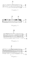
- Fig. 1 is a schematic section view showing a metallic material for electric / electronic component of one embodiment of the invention.
- the metallic material for electric / electronic component of the mode shown in Fig. 1 is obtained by plating Sn on the conductive base 1, by treating by heat and by provided the Cu-Sn alloy layer 2 whose Cu concentration is gradually reduced from the side of the base 1 to the side of the surface (material surface) 3 for example.
- the copper material or a Cu base material coated with copper or a copper alloy is used as the conductive base 1.
- Cu components of the Cu base material coated with copper or the copper alloy on the surface of the conductive base 1 thermally diffuse into the Sn plating layer and Sn also diffuses into the base 1 by the heat treatment in this mode. Due to that, the Cu-Sn alloy layer 2 whose Cu concentration is gradually reduced from the base side 1 to the surface 3 is formed. No clear boundary between the conductive base 1 and the Cu-Sn alloy layer 2 in section is also formed.
- Fig. 2 is a schematic section view showing a metallic material for electric / electronic component of another one embodiment of the invention.
- the metallic material for electric / electronic component of the mode shown in Fig. 2 is obtained by coating the conductive base 1 with Sn plating or the like, by treating by heat to provide the Cu-Sn alloy layer 2 whose Cu concentration is gradually reduced from the side of the base 1 to the side of the surface 3 and Sn (4) is partially dispersed within the Cu-Sn alloy layer 2.
- the material of the conductive base 1 and the boundary between the conductive base 1 and the Cu-Sn alloy layer 2 are the same with the mode shown in Fig. 1 .
- the Sn (4) may be metallic Sn or a Sn alloy (containing Sn by more than 50 mass %).
- the metallic Sn or the Sn alloy is dispersed by optimizing conditions of the heat treatment such as the reflow process and the batch process so that the coated Sn is not totally alloyed with the base 1 or with Cu existing on the surface thereof (specifically, the heat treatment is finished before the coated Sn is totally alloyed with the base 1 or Cu existing on the surface thereof).
- the dispersion state is preferable if at least part of the metallic Sn and the Sn alloy (Sn concentration is more than 80 mol %) is exposed on the surface of the uppermost layer and Sn or the Sn alloy is dispersed like an island or a dot when seen planarly. Still more, an oxide film from 0 to 100 nm may be formed on the outermost layer.
- a still other embodiment of the invention is the metallic material for electric / electronic component in which the conductive base 1 coated with any one type of metal among Ni, Co and Fe or with an alloy containing those metals as a main component (more than 50 mass %) by plating and is then treated by heat to provide the Cu-Sn alloy layer 2 whose Cu concentration is gradually reduced from the base side 1 toward the surface 3.
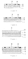
- Fig. 3 is a schematic section view showing a metallic material for electric / electronic component of the present embodiment in which the conductive base 1 is coated with Cu by plating or the like.
- the conductive base 1 is provided with a Cu layer 5 and the Cu layer 5 is coated with Sn by plating or the like.
- Fig. 4 is a schematic section view showing a metallic material for electric / electronic component of the present embodiment in which the conductive base 1 is plated with Ni.
- the conductive base 1 is coated with a Ni layer (undercoat) 6 by plating or the like and the Ni layer 6 is coated further with a Cu layer and a Sn layer in this order by plating or the like.
- the heat treatment is implemented, so that the Cu layer provided on the Ni layer 6 and the Sn plating layer provided thereon mutually diffuse and the Cu-Sn alloy layer 2 whose Cu concentration is gradually reduced from the base side to the surface side is formed.
- the similar metallic material for electric / electronic component may be obtained also when Co plating or Fe plating is implemented instead of the Ni plating.
- a still different embodiment of the invention is the metallic material for electric / electronic component in which the conductive base 1 coated with any one type of metal among Ni, Co and Fe or with an alloy containing those metals as a main component (more than 50 mass %) by plating or the like, is coated with Cu and Sn in this order and is then treated by heat to provide the Cu-Sn alloy layer 2 whose Cu concentration is gradually reduced from the base side 1 toward the surface 3 and Sn or the Sn alloy is partially dispersed within the Cu-Sn alloy layer 2.
- Fig. 5 is a schematic section view showing a metallic material for electric / electronic component of the present embodiment in which the conductive base 1 is coated with Cu by plating or the like.
- the conductive base 1 is provided with the Cu layer 5 and the Cu layer 5 is coated with Sn by plating or the like. Then, a heat treatment is implemented, so that Cu components thermally diffuse from the Cu layer 5 into the Sn layer and Sn also diffuses into the Cu layer 5. Therefore, the Cu-Sn alloy layer 2 whose Cu concentration is gradually reduced from the side of the base 1 to the side of the surface 3 is formed. No clear boundary between the Cu layer 5 and the Cu-Sn alloy layer 2 in section is formed.
- the Sn (4) is partially dispersed within the Cu-Sn alloy layer 2. The method for dispersing the Sn (4) is the same with the dispersing method in the mode show in Fig. 2 described above.
- Fig. 6 is a schematic section view showing a metallic material for electric / electronic component of the present embodiment in which the conductive base 1 is plated with Ni.
- the conductive base 1 is coated with a Ni layer 6 by plating or the like and the Ni layer 6 is coated further with a Cu layer and a Sn layer in this order by plating or the like.
- the heat treatment is implemented, so that the Cu layer provided on the Ni layer 6 and the Sn plating layer provided thereon mutually diffuse and the Cu-Sn alloy layer 2 whose Cu concentration is gradually reduced from the base side to the surface side is formed.
- the Sn (4) is partially dispersed within the Cu-Sn alloy layer 2.
- the method for dispersing the Sn (4) is the same with the dispersing method in the mode shown in Fig. 2 described above.
- a still different embodiment of the invention is a metallic material for electric / electronic component in which the conductive base 1 coated with any one type of metal among Ni, Co and Fe or with an alloy containing those metals as a main component (more than 50 mass %) by two layers by plating or the like, is coated with Cu and Sn in this order and is then treated by heat to provide the Cu-Sn alloy layer 2 whose Cu concentration is gradually reduced from the base side 1 toward the surface 3.
- a combination of two types of plating implemented on the conductive base 1 is not specifically limited.
- Fig. 7 is a schematic section view showing a metallic material for electric / electronic component of the present embodiment in which the conductive base 1 is coated with Ni as an under layer and with Cu as an upper layer by plating or the like.
- the conductive base 1 is coated with a Ni layer 6 and a Cu layer 5 in this order and the Cu layer 5 is coated further with a Sn layer by plating or the like.
- the heat treatment is implemented, so that the Cu components thermally diffuse from the Cu layer 5 to the Sn layer and Sn also diffuses into the Cu layer 5 by the heat treatment described above. Due to that, the Cu-Sn alloy layer 2 whose Cu concentration is gradually reduced from the base side to the surface side is formed. No clear boundary between the Cu layer 5 and the Cu-Sn alloy layer 2 in section is formed.
- a still other embodiment of the invention is a metallic material for electric / electronic component in which the conductive base 1 coated with any one type of metal among Ni, Co and Fe or with an alloy containing those metals as a main component (more than 50 mass %) by two layers by plating or the like, is coated with Cu and Sn in this order by plating or the like and is then treated by heat to provide the Cu-Sn alloy layer 2 whose Cu concentration is gradually reduced from the base side 1 toward the surface 3 and Sn or the Sn alloy is partially dispersed within the Cu-Sn alloy layer 2.
- a combination of two types of plating implemented on the conductive base 1 is not specifically limited.
- Fig. 8 is a schematic section view showing a metallic material for electric / electronic component of the present embodiment in which the conductive base 1 is coated with Ni as an under layer and with Cu as an upper layer by plating or the like.
- the conductive base 1 is coated with a Ni layer 6 and a Cu layer 5 in this order and the Cu layer 5 is coated further with a Sn layer by plating or the like.
- the heat treatment is implemented, so that the Cu components thermally diffuse from the Cu layer 5 into the Sn layer and Sn also diffuses into the Cu layer 5 by the heat treatment described above.
- the Cu-Sn alloy layer 2 whose Cu concentration is gradually reduced from the base side to the surface side is formed. No clear boundary between the Cu layer 5 and the Cu-Sn alloy layer 2 in section is formed. Sn (4) or the Sn alloy is partially dispersed within the Cu-Sn alloy layer 2. The method for dispersing the Sn (4) is the same with the dispersing method in the mode shown in Fig. 2 described above.
- the Cu-Sn alloy layer in the outermost layer contains a Cu-Sn intermetallic compound layer in the present invention.
- the Cu-Sn intermetallic compound in the invention includes Cu 6 Sn 5 , Cu 3 Sn and others.
- the invention includes those in which those intermetallic compounds are mixed.
- the conductive base 1 is provided with the undercoat such as the Ni layer 6 as described in the modes shown in Figs, 4 , 6, 7 and 8 . It becomes possible to prevent the components of the base 1 from diffusing into the outermost layer by providing the undercoat.
- the undercoat provided on the conductive base 1 metals such as Ni, Co and Fe having a barrier function for preventing the component of the base from thermally diffusing into the outermost layer and Ni-P, Ni-Sn, Co-P, Ni-Co, Ni-Co-P, Ni-Cu, Ni-Cr, Ni-Zn, Ni-Fe and other alloys may be suitably used. These metals and alloys have favorable plating treatability and have no problem in terms of their cost. Among them, Ni and Ni alloy are recommended because their barrier function does not deteriorate even under a high-temperature environment.
- the undercoat While a fusion point of the metal (alloy) such as Ni used for the undercoat described above is as high as 1000° C, temperature of use environment of the connector is lower than 200° C, so that the undercoat itself hardly causes thermal diffusion and its barrier function is effectively exhibited.
- the undercoat also has a function of enhancing adhesion between the conductive base and an intermediate layer described later depending on a material of the conductive base.
- the barrier function of the undercoat is not fully exhibited if its thickness is under 0.01 ⁇ m and plating distortion thereof becomes large and the undercoat is prone to fall away if the thickness exceeds 3 ⁇ m. Accordingly, the thickness of the undercoat is preferable to be in a range from 0.01 to 3 ⁇ m. Considering a terminal workability, an upper limit of the thickness of the undercoat is preferable to be 1.5 ⁇ m or more preferable to be 0.5 ⁇ m.
- the metallic material for electric / electronic component of the present invention is what the conductive base 1 is provided with the intermediate layer composed of the Cu layer 5 on the undercoat made of Ni or the like as described in the mode shown in Figs. 7 and 8 . It becomes possible to prevent the component of the undercoat such as Ni from diffusing into the outermost layer, to stably obtain favorable electrical connectivity and to readily form the Cu-Sn alloy layer whose Cu concentration is gradually reduced from the base side to the surface by providing the intermediate layer.
- a thickness of the intermediate layer is preferable to be 0.01 to 3um or more preferable to be 0.1 to 0.5 ⁇ m.
- the metallic material for electric / electronic component of the invention may be formed into any shape such as a strip, round wire and rectangular wire.
- the metallic material for electric / electronic component of the invention may be worked into an electric / electronic part such as a fitting-type multipole connector for use in automobiles by a normal method.
- a connector created by using the metallic material for electric / electronic component of the invention may be what weakens a contact pressure between terminals, causes no fretting phenomenon between contact faces of terminals and suppresses an occurrence of inferior conductivity between the terminals.
- the metallic material for electric / electronic component of the invention may be manufactured readily by a reflow thermal treatment and may improve heat resistance of a plating material. It is because the abundant Cu on the base side reacts with the abundant Sn on the surface side within the Cu-Sn alloy layer even under a high-temperature environment when this material is used as an electric / electronic material. Still more, the electric / electronic material manufactured by using the metallic material for electric / electronic component of the invention can remarkably suppress a sharp rise of resistance (fretting) at an electrical contact during sliding.
- the metallic material for electric /electronic component in which the conductive base is provided with the undercoat made of Ni or the like can prevent the components of the base from diffusing into the outermost layer.
- the material in which the intermediate layer made of Cu or the like is provided on the undercoat can prevent the component such as Ni of the base from diffusing into the outermost layer. Accordingly, it becomes possible to stably obtain favorable electrical connectivity.
- the material in which Sn or the Sn alloy is partially dispersed within the Cu-Sn alloy layer has the effect that no CuO and the like is formed by exposed Cu and the contact resistance is stabilized because there is such a room that a Cu-Sn alloy is formed as Cu existing under the Cu-Sn alloy layer reacts with Sn or the Sn alloy dispersed within the Cu-Sn alloy layer.
- a plated laminate was fabricated by degreasing and pickling a copper strip of 0.25 mm thick in this order and by electroplating the copper alloy strip by laminating Ni, Cu and Sn in this order.
- Plating of each metal was implemented under the following conditions: (a) Ni Plating - Plating Bath Composition Component: Concentration: Nickel sulfamate 500 g/l Boric acid 30 g/l - Bath Temperature: 60° C - Electrical Density: 5A/dm 2 - Thickness of Plating: 0.5 ⁇ m (b) Cu Plating - Plating Bath Composition Component: Concentration: Copper sulfate 180 g/l Sulfuric acid 80 g/l - Bath Temperature: 40° C - Electrical Density: 5A/dm 2 - Thickness of Plating: 0.8 ⁇ m (c) Sn Plating - Plating Bath Composition Component: Concentration: Stannous sulfate 80
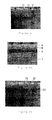
- Fig. 9 shows a photograph (horizontal width : 11.7 ⁇ m) of this material taken by SEM (Scanning Electron Microscope) and Fig. 10 shows an electronic image (Cu-Sn-Ni map) taken by AES (Auger Electron Spectroscopy) of a measured section containing the surface shown in the SEM photograph.
- This measurement was carried out by preparing a sample for AES analysis with a sample angle of 60 degrees and an oblique section of 30 degrees by FIB (Focused Ion Beam) at first, by analyzing the sample by inclining so that the oblique section of 30 degrees of the AES analysis becomes horizontal and by measuring the thickness of each layer by obtaining AES images.
- Table 1 shows Sn and Cu concentrations (mol%) in the respective measuring surface 1 (11), 2(12) and 3 (13) shown in Fig. 9 found by AES qualitative analysis:
- the material of the present embodiment is formed such that the Cu layer 5 and the Cu-Sn alloy layer 2 are formed on the Ni layer 6 substantially continuously and the Cu concentration is gradually reduced from the base side toward the surface.
- a plated laminate was fabricated by degreasing and pickling a copper strip of 0.25 mm thick in this order and by electroplating the copper alloy strip by laminating Ni, Cu and Sn in this order.
- Plating of each metal was implemented under the following conditions: (a) Ni Plating - Plating Bath Composition Component: Concentration: Nickel sulfamate 500 g/l Boric acid 30 g/l - Bath Temperature: 60° C - Electrical Density: 5A/dm 2 - Thickness of Plating: 0.5 ⁇ m (b) Cu Plating - Plating Bath Composition Component: Concentration: Copper sulfate 180 g/l Sulfuric acid 80 g/l - Bath Temperature: 40° C - Electrical Density: 5A/dm 2 - Thickness of Plating: 0.8 ⁇ m (c) Sn Plating - Plating Bath Composition Component: Concentration: Stannous sulfate 80
- Fig. 11 shows a photograph (horizontal width: 11.7 ⁇ m) of this material taken by SEM and Fig. 12 shows an electronic image (Cu-Sn-Ni map) taken by AES of a measured section containing the surface shown in the SEM photograph in Fig. 11 .
- Table 2 shows Sn and Cu concentrations (mol%) in the respective measuring surface 1 (21), 2(22) and 3 (23) shown in Fig. 11 found by AES qualitative analysis:
- the material of the present embodiment is formed such that the Ni layer 6, the Cu layer 5 and the Cu-Sn alloy layer 2 are formed on the base 1 in this order, the boundary between the Cu layer 5 and the Cu-Sn alloy layer 2 is not clear and the Cu concentration is gradually reduced from the base side toward the surface. Still more, the Sn (4) is dispersed like an island within the Cu-Sn alloy layer 2.
- the following fine sliding test was carried out on the respective metallic materials for electric / electronic component obtained in the first and second exemplary embodiments by sliding and reciprocating the material up to 1,000 times to measure changes of values of contact resistance continuously.
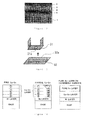
- the fine sliding test was carried out by preparing two each pieces of testing metallic materials 31 and 32, by providing a semi-spherical bulge section (convex outer surface is the outermost layer surface) 31a having a radius of curvature of 1.8 mm in the testing metallic material piece 31, by contacting an outermost layer surface 32a of the testing metallic material piece 32 after degreasing and washing, respectively, to the semi-spherical bulge section 31a with contact pressure 3N, by reciprocating and sliding the both in this state with 30 ⁇ m of a sliding distance under an environment of 20° C of temperature and 65 & of humidity, by flowing 5 mA of constant current while loading 20 mV of open voltage between the both testing metallic material pieces 31 and 32 and by finding the changes of electric resistance per one second by measuring a voltage drop during sliding by a four-terminal method.
- frequency of the reciprocal movement was about 3.3 Hz.
- the value of contact resistance before the fine sliding test was 0.1 m ⁇ when the testing metallic material pieces 31 and 32 are used as the materials of the first embodiment and was 0.5 m ⁇ when used as the materials of the second embodiment.
- the maximum contact resistance value during the fine sliding test was 4.0 m ⁇ when the testing metallic material pieces 31 and 32 are used as the materials of the first embodiment and was 4.1 m ⁇ when used as the materials of the second embodiment.
- a plated laminate was fabricated by plating a copper alloy strip by laminating Ni, Cu and Sn in the same manner with the firs embodiment and the same heat treatment was implemented to obtain each metallic material.
- thicknesses of plating of Cu and Sn are those in the Cu-Sn layer in the following Table 3 and no Ni plating is implemented in the case when there is no undercoat Ni layer.
- Each metallic material thus obtained was tested as a specimen piece and Table 3 shows their plating modes and evaluation results:
- the test Nos. 9, 10, 17 and 18 whose Cu-Sn alloy layer is out of the range of 0.1 to 3.0 ⁇ m have inferior fretting resistance and heat resistance after sliding as compared to the test Nos. 1 through 5 and 11 through 15 that are within the range. Further, when the thickness of the Cu-Sn layer is thicker than 3.0 ⁇ m, they are inferior than the test Nos. 1 through 15 and 11 through 15 in the test of after-thermal load of 160° C x 120h as indicated by the test Nos. 9 and 17.
- the thickness of the Cu-Sn layer is thinner than 0.1 ⁇ m, they are inferior not only in the test after-thermal load of 160° C x 120h but also in the test after spraying salt water and after corroding by gas as indicated by the test Nos. 10 and 18.
- a plated laminate was fabricated by plating Ni, Cu and Sn on the strip of copper alloy in the same manner with the first embodiment and a heat treatment was implemented to obtain each metallic material for electric / electronic component shown in the following Table 4.
- the thicknesses of plating of Cu and Sn are thickness indicated by thicknesses of Cu and Sn in Table 4 and no Ni plating is implemented in the case when there is no undercoat Ni layer in Table 4.
- Each metallic material thus obtained was tested as specimen and Table 4 shows their plating mode and evaluation results.
- the degree of decrease of the test No, 35 whose heating temperature is as high as 900° C is small.
- the fretting resistance of the test Nos. 31 through 35 having the pure Sn layer on the outermost surface isinferior. Still more, the test Nos. 32 and 34 whose heating and cooling times are short have inferior heat resistance after sliding.
- the metallic material for electric / electronic component of the invention may be readily manufactured and may be suitably used for a connecting or sliding portion of a connector terminal.
Landscapes
- Chemical & Material Sciences (AREA)
- Engineering & Computer Science (AREA)
- Chemical Kinetics & Catalysis (AREA)
- Electrochemistry (AREA)
- Materials Engineering (AREA)
- Metallurgy (AREA)
- Organic Chemistry (AREA)
- Electroplating Methods And Accessories (AREA)
- Conductive Materials (AREA)
- Non-Insulated Conductors (AREA)
Abstract
Description
- The present invention relates to a metallic material for electric / electronic component suitable for a sliding portion of a fitting-type multipole connector and the like.
- A plating material provided with a plating layer of tin (Sn), a tin alloy and others on a conductive base such as copper (Cu) and a copper alloy (appropriately referred to as a base hereinafter) is known to be a high-performance conductor having excellent conductivity and strength of the base and excellent electrical connectivity, corrosion resistance and soldering quality of the plating layer and is widely used as various terminals and connectors for use in electric / electronic devices. This plating material is normally undercoated with nickel (Ni), cobalt (Co), iron (Fe) and others having a barrier function on the base in order to prevent an alloy component (appropriately referred to as a base component hereinafter) such as zinc (Zn) from diffusing on the plating layer.
- When this plating material is used as a terminal in a high-temperature environment such as an inside of an engine room of a vehicle for example, although an oxide coating film is formed on the surface of the Sn plating layer because the Sn plating layer on the surface of the terminal is oxidizable, this oxide coating film is brittle, so that it breaks down when the terminal is connected and non-oxidized Sn plating layer is exposed, allowing to obtain favorable electrical connectivity.
- By the way, because a fitting-type multipole connector is multipolarized lately in the advancement of electronic control, a considerable force is necessary in plugging a male terminal group into/out of a female terminal group. In particular, this work of plugging such connector is difficult in a narrow space such as the engine room of the vehicle, it has been strongly demanded to be able to reduce the force for plugging in/out such connector. Still more, workability in connecting the connector is improved by reducing the force for plugging in/out the connector, it has been demanded to reduce the force for plugging in/out the connector also from this point of view.
- While a method of thinning the Sn plating layer on the surface of the connector terminal to weaken contact pressure between the terminals as a method for reducing the plugging-in/out force, this method may cause a fretting phenomenon between the contact faces of the terminals, causing inferior conduction between the terminals, because the Sn plating layer is soft.
- The fretting phenomenon is a phenomenon by which the soft Sn plating layer on the surface of the terminal wears and is oxidized, becoming abrasion powder having large specific resistance, due to fine vibration that occurs between the contact faces of the terminals caused by vibration and changes in temperature. The lower the contact pressure between the terminals, the more this phenomenon is prone to occur.
- With regard to this, aiming at assuring the property of low plugging force and others, Japanese Patent Application Laid-Open No.
2000-226645 2000-226645 - Still more, aiming also at assuring the property of low plugging force and others, Japanese Patent Application Laid-Open No.
2004-68026 - Japanese Patent Application Laid-Open No.
2004-339555 - Japanese Patent Application Laid-Open No.
2006-77307
However, even if there would be no problem when there is no Cu layer in a substrate and when there exists a Ni substrate and even if there would be no problem in an initial state when the Cu layer exists and no Ni substrate exists, it is considered that if the pure Sn portion is scraped due to sliding under an environment in which the connecting component is mounted in an actual car and in which sliding and thermal load are applied in the same time, Cu diffuses up to the surface and is oxidized, soon increasing resistance in the end. - That is, the invention provides the following means:
- (1) A metallic material for electric / electronic component in which a Cu-Sn alloy layer is provided on a conductive base, characterized in that Cu concentration in the Cu-Sn alloy layer gradually decreases from the base side toward the surface side;
- (2) A metallic material for electric / electronic component in which a Cu-Sn alloy layer is provided on a conductive base, characterized in that Cu concentration in the Cu-Sn alloy layer gradually decreases from the base side toward the surface side and that Sn or Sn alloy is dispersed partially within the Cu-Sn alloy layer;
- (3) A metallic material for electric / electronic component in which any one type of metal among Ni, Co and Fe or an alloy containing those metals is provided on the a conductive base and a Cu-Sn alloy layer is provided further thereon, characterized in that Cu concentration in the Cu-Sn alloy layer gradually decreases from the base side toward the surface side;
- (4) A metallic material for electric / electronic component in which any one type of metal among Ni, Co and Fe or an alloy containing those metals is provided on the a conductive base and a Cu-Sn alloy layer is provided further thereon, characterized in that Cu concentration in the Cu-Sn alloy layer gradually decreases from the base side toward the surface side and that Sn or Sn alloy is dispersed partially within the Cu-Sn alloy layer;
- (5) A metallic material for electric / electronic component in which two layers of any one type of metal among Ni, Co and Fe or an alloy containing those metals are provided on the a conductive base and a Cu-Sn alloy layer is provided further thereon, characterized in that Cu concentration in the Cu-Sn alloy layer gradually decreases from the base side toward the surface side;
- (6) A metallic material for electric / electronic component in which two layers of any one type of metal among Ni, Co and Fe or an alloy containing those metals are provided on the a conductive base and a Cu-Sn alloy layer is provided further thereon, characterized in that Cu concentration in the Cu-Sn alloy layer gradually decreases from the base side toward the surface side and that Sn or Sn alloy is dispersed partially within the Cu-Sn alloy layer;
- (7) The metallic material for electric / electronic component according to any one of the first, third and fifth aspects, characterized in that the Cu concentration in the half of the Cu-Sn alloy layer on the base side is 50 to 100 mol% and Sn concentration thereof is 0 to 50 mol% and that the Cu concentration in the half on the surface side is 40 to 95 mol% and the Sn concentration is 5 to 60 mol%.
- (8) The metallic material for electric / electronic component according to any one of the second, fifth and sixth aspects, characterized in that the Cu concentration in the half of the Cu-Sn alloy layer on the base side is 50 to 100 mol% and Sn concentration thereof is 0 to 50 mol% and that the Cu concentration in the half on the surface side is 0 to 95 mol% and the Sn concentration is 5 to 100 mol%.
- (9) The metallic material for electric / electronic component according to any one of the first through eighth aspects, characterized in that the Cu-Sn alloy layer is 0.1 to 3.0 µm thick.
- (10) A method for manufacturing the metallic material for electric / electronic component according to any one of the first through ninth aspects, characterized in that the method includes steps of fabricating a laminate by laminating Cu and Sn in this order on the conductive base or any one type of the metals of Ni, Co and Fe or the alloy containing those metals, implementing a heat treatment on the laminate and implementing a cooling process on the laminate treated by heat.
- (11) The method for manufacturing the metallic material for electric / electronic component according to the tenth aspect, characterized in that the heat treatment is a process of passing the laminate within a reflow furnace whose in-furnace temperature is higher than 300° C and lower than 900° C for three to 20 seconds;
- (12) The method for manufacturing the metallic material for electric / electronic component according to the tenth aspect, characterized in that the cooling process is a process of passing the laminate within a liquid of 20 to 80° C for one to 300 seconds; and
- (13) The method for manufacturing the metallic material for electric / electronic component according to the tenth aspect, characterized in that the cooling process is a process of passing the laminate within a gas of 20 to 60° C for one to 300 seconds and then passing the laminate within the liquid of 20 to 80° C for one to 100 seconds.
- The abovementioned and other features and advantages of the invention will be more apparent from the following description understood by appropriately making reference to the appended drawings.
-
- [
FIG. 1] FIG. 1 is a longitudinal section view showing one mode of a metallic material for electric / electronic component the invention. - [
FIG. 2] FIG. 2 is a longitudinal section view showing one mode of the metallic material for electric / electronic component the invention. - [
FIG. 3] FIG. 3 is a longitudinal section view showing one mode of the metallic material for electric / electronic component the invention. - [
FIG. 4] FIG. 4 is a longitudinal section view showing one mode of the metallic material for electric / electronic component the invention. - [
FIG. 5] FIG. 5 is a longitudinal section view showing one mode of the metallic material for electric / electronic component the invention. - [
FIG. 6] FIG. 6 is a longitudinal section view showing one mode of the metallic material for electric / electronic component the invention. - [
FIG. 7] FIG. 7 is a longitudinal section view showing one mode of the metallic material for electric / electronic component the invention. - [
FIG. 8] FIG. 8 is a longitudinal section view showing one mode of the metallic material for electric / electronic component the invention. - [
Fig. 9] Fig. 9 is a microscope photograph, taken by a SEM, of the metallic material for electric / electronic component of a first embodiment. - [
Fig. 10] Fig. 10 is a Cu-Sn-Ni map of the first embodiment. - [
Fig. 11] Fig. 11 is a microscope photograph, taken by the SEM, of the metallic material for electric / electronic component of a second embodiment. - [
Fig. 12 ]Fig. 10 is a Cu-Sn-Ni map of the second embodiment. - [
Fig. 13] Fig. 13 is a perspective explanatory diagram of a fine vibration testing method of a test example 1. - [
Fig. 14] Fig. 14 is an explanatory diagram diagrammatically showing layered structures to explain sections of sample materials of third and fourth embodiments. - A metallic material for electric / electronic component of the present invention is provided with a Cu-Sn alloy layer on a conductive base or on an undercoat formed on the conductive base and Cu concentration in the Cu-Sn alloy layer gradually decreases from the side of the base toward the side of a surface of the metal material. This metallic material for electric / electronic component is formed by forming the Cu-Sn alloy layer by plating Sn on a plating layer formed on the conductive base and by implementing a heat treatment and by decreasing the Cu concentration gradually from the base side to the surface side.
The phrase "the Cu concentration of the Cu-Sn alloy layer gradually decreases from the base side to the surface" means that the cu measured at least three places whose depth from the surface of the layer is different in section of the Cu-Sn alloy layer is low in order closer to the surface. - While the Cu concentration of the Cu-Sn alloy layer of the invention gradually decreases from the base side to the surface, the Cu concentration in a half of the base side of the thickness is preferable to be 50 to 100 mol% and is more preferable to be 65 to 100 mol% and the Sn concentration is preferable to be 0 to 50 mol% of the remaining part and more preferable to be 0 to 35 mol% (this is concentration in which inevitable impurities other than Cu and Sn are neglected. The same applies hereinafter).
In a case when Sn or the Sn alloy is not distributed partially, the Cu concentration on a half on the surface side is preferable to be 40 to 95 mol% and more preferable to be 65 to 85 mol%. The Sn concentration is preferable to be 5 to 60 mol% and more preferable to be 15 to 35 mol%. In a case when Sn or the Sn alloy is dispersed partially, the Cu concentration in the half of the surface side is preferable to be 0 to 95 mol% and more preferable to be 65 to 85 mol%. The Sn concentration is preferable to be 5 to 100 mol% and more preferable to be 15 to 35 mol%.
If the Cu concentration in the half of the base side is too low (the Sn concentration is too high), a pure Sn layer tends to be formed on the outermost surface and fretting resistance deteriorates.
If the Sn concentration in the half of the surface side is too low, the heat resistance decreases, leading to the quick increase of resistance when used under a high-temperature environment. - The metallic material for electric / electronic component of the invention has a room for permitting Cu to diffuse with Sn even if a Cu layer exists in a substrate or no Ni substrate exists because the Cu-Sn alloy layer is what is formed so that the Cu concentration within the Cu-Sn alloy layer on the upper side in gradation, i.e., the Sn concentration is low in the Cu-Sn alloy layer on the surface side. As a result, it becomes possible to retard Cu from being exposed on the outermost surface and being oxidized even if the metallic material for electric / electronic component receives thermal load.
A thickness of the Cu-Sn alloy layer is preferably in a range from 0.1 to 3.0 µm and more preferable to be 0.3 to 1.5 µm. If this thickness is too thick, Kirkendall voids tend to be generated in a diffusion process, possibly causing delamination of plating. Still more, it is presumed that costs for plating increase due to the increase of heat-treatment temperature and time. If the thickness is too thick, the contact resistance may increase, the heat resistance may be deteriorated and the fretting resistance may be deteriorated. - In the present invention, copper and copper alloys such as phosphor bronze, brass, alpaca, beryllium copper and Corson alloy, iron and iron alloys such as stainless steel, compound materials such as copper-coated steel material and nickel-coated steel material, various nickel alloy and aluminum alloys having conductivity, mechanical strength and heat resistance required for terminals may be used for the conductive base.
- Among the metals and alloys (material) described above, the copper materials such as copper and the copper alloys are suitable in particular because they excel in the balance of the conductivity and mechanical strength. If the conductive base is made of materials other than the copper material, it is preferable to coat copper or the copper alloy on the surface of the conductive base.
- While the Sn plating may be formed by nonelectrolytic plating, it is desirable to form by electroplating. A thickness of the Sn layer formed by the Sn plating is preferable to be in a range from 0.01 to 5.0 µm.
Sn electroplating of the uppermost layer may be carried out under conditions of 30°C or less of plating temperature and 5A/cm2 of current density by employing tin sulfate bath for example. However, these conditions are not limited to these and may be appropriately set. - According to the invention, the laminate material whose uppermost layer is Sn-plated is treated by heat. Conditions for this heat treatment are selected so as to form the Cu-Sn alloy layer in which the Cu concentration gradually decreases from the base side to the surface side. When the heat treatment is implemented by a reflow process (continuous process), it is preferable to heat in an in-furnace temperature range of 300°C or more to under 900°C for three to 20 seconds (or preferably from 5 to 10 seconds or more preferably from 6 to 8 seconds).
These temperature and time are adopted to obtain the Cu-Sn alloy layer whose Cu concentration gradually decreases from the base side to the surface side.
It is noted that it is preferable to hold the material described above for 0.1 to 200 hours within a furnace whose temperature is 60 to 200° C when the heat treatment is carried out in a way of batch process. - Still more, it is preferable to pass the laminate material treated by heat by the reflow process into liquid within a cooling tank by taking 1 to 100 seconds (or more preferably 3 to 10 seconds) to quench the material. Temperature of the liquid is preferable to be in a range from 20 to 80° C (or more preferably 30 to 50° C). It is also preferable to pass the laminate material treated by heat into gas of a cold-air unit within the in-furnace atmosphere of 20 to 60° C by taking 1 to 300 seconds to gradually cool the material.
It becomes possible to obtain the plating structure in which the Cu concentration within the Cu-Sn alloy layer is gradational and to disperse pure Sn within the Cu-Sn alloy layer by forcibly ending the diffusion of Cu and Sn in mid-stream or by rapidly reducing their diffusion speed by such cooling process. -
Fig. 1 is a schematic section view showing a metallic material for electric / electronic component of one embodiment of the invention. The metallic material for electric / electronic component of the mode shown inFig. 1 is obtained by plating Sn on theconductive base 1, by treating by heat and by provided the Cu-Sn alloy layer 2 whose Cu concentration is gradually reduced from the side of thebase 1 to the side of the surface (material surface) 3 for example. In this mode, the copper material or a Cu base material coated with copper or a copper alloy is used as theconductive base 1. By treating by heat as described above, Cu components of the Cu base material coated with copper or the copper alloy on the surface of theconductive base 1 thermally diffuse into the Sn plating layer and Sn also diffuses into thebase 1 by the heat treatment in this mode. Due to that, the Cu-Sn alloy layer 2 whose Cu concentration is gradually reduced from thebase side 1 to thesurface 3 is formed. No clear boundary between theconductive base 1 and the Cu-Sn alloy layer 2 in section is also formed. -
Fig. 2 is a schematic section view showing a metallic material for electric / electronic component of another one embodiment of the invention. The metallic material for electric / electronic component of the mode shown inFig. 2 is obtained by coating theconductive base 1 with Sn plating or the like, by treating by heat to provide the Cu-Sn alloy layer 2 whose Cu concentration is gradually reduced from the side of thebase 1 to the side of thesurface 3 and Sn (4) is partially dispersed within the Cu-Sn alloy layer 2. The material of theconductive base 1 and the boundary between theconductive base 1 and the Cu-Sn alloy layer 2 are the same with the mode shown inFig. 1 . The Sn (4) may be metallic Sn or a Sn alloy (containing Sn by more than 50 mass %). While any method may be used for dispersing the Sn (4), the metallic Sn or the Sn alloy is dispersed by optimizing conditions of the heat treatment such as the reflow process and the batch process so that the coated Sn is not totally alloyed with thebase 1 or with Cu existing on the surface thereof (specifically, the heat treatment is finished before the coated Sn is totally alloyed with thebase 1 or Cu existing on the surface thereof).
The dispersion state is preferable if at least part of the metallic Sn and the Sn alloy (Sn concentration is more than 80 mol %) is exposed on the surface of the uppermost layer and Sn or the Sn alloy is dispersed like an island or a dot when seen planarly. Still more, an oxide film from 0 to 100 nm may be formed on the outermost layer. - A still other embodiment of the invention is the metallic material for electric / electronic component in which the
conductive base 1 coated with any one type of metal among Ni, Co and Fe or with an alloy containing those metals as a main component (more than 50 mass %) by plating and is then treated by heat to provide the Cu-Sn alloy layer 2 whose Cu concentration is gradually reduced from thebase side 1 toward thesurface 3.
Fig. 3 is a schematic section view showing a metallic material for electric / electronic component of the present embodiment in which theconductive base 1 is coated with Cu by plating or the like. In the metallic material for electric /electronic component of the mode shown inFig. 3 , theconductive base 1 is provided with aCu layer 5 and theCu layer 5 is coated with Sn by plating or the like. Then, a heat treatment is implemented so that Cu components thermally diffuse from theCu layer 5 into the Sn layer and Sn also diffuses into theCu layer 5. Therefore, the Cu-Sn alloy layer 2 whose Cu concentration is gradually reduced from the side of thebase 1 to the side of thesurface 3 is formed. No clear boundary between theCu layer 5 and the Cu-Sn alloy layer 2 in section is also formed. -
Fig. 4 is a schematic section view showing a metallic material for electric / electronic component of the present embodiment in which theconductive base 1 is plated with Ni. In the metallic material for electric / electronic component of the mode shown inFig. 4 , theconductive base 1 is coated with a Ni layer (undercoat) 6 by plating or the like and theNi layer 6 is coated further with a Cu layer and a Sn layer in this order by plating or the like. Here, the heat treatment is implemented, so that the Cu layer provided on theNi layer 6 and the Sn plating layer provided thereon mutually diffuse and the Cu-Sn alloy layer 2 whose Cu concentration is gradually reduced from the base side to the surface side is formed. The similar metallic material for electric / electronic component may be obtained also when Co plating or Fe plating is implemented instead of the Ni plating. - A still different embodiment of the invention is the metallic material for electric / electronic component in which the
conductive base 1 coated with any one type of metal among Ni, Co and Fe or with an alloy containing those metals as a main component (more than 50 mass %) by plating or the like, is coated with Cu and Sn in this order and is then treated by heat to provide the Cu-Sn alloy layer 2 whose Cu concentration is gradually reduced from thebase side 1 toward thesurface 3 and Sn or the Sn alloy is partially dispersed within the Cu-Sn alloy layer 2.
Fig. 5 is a schematic section view showing a metallic material for electric / electronic component of the present embodiment in which theconductive base 1 is coated with Cu by plating or the like. In the metallic material for electric /electronic component of the mode shown inFig. 5 , theconductive base 1 is provided with theCu layer 5 and theCu layer 5 is coated with Sn by plating or the like. Then, a heat treatment is implemented, so that Cu components thermally diffuse from theCu layer 5 into the Sn layer and Sn also diffuses into theCu layer 5. Therefore, the Cu-Sn alloy layer 2 whose Cu concentration is gradually reduced from the side of thebase 1 to the side of thesurface 3 is formed. No clear boundary between theCu layer 5 and the Cu-Sn alloy layer 2 in section is formed. The Sn (4) is partially dispersed within the Cu-Sn alloy layer 2. The method for dispersing the Sn (4) is the same with the dispersing method in the mode show inFig. 2 described above. -
Fig. 6 is a schematic section view showing a metallic material for electric / electronic component of the present embodiment in which theconductive base 1 is plated with Ni. In the metallic material for electric / electronic component of the mode shown inFig. 6 , theconductive base 1 is coated with aNi layer 6 by plating or the like and theNi layer 6 is coated further with a Cu layer and a Sn layer in this order by plating or the like. Here, the heat treatment is implemented, so that the Cu layer provided on theNi layer 6 and the Sn plating layer provided thereon mutually diffuse and the Cu-Sn alloy layer 2 whose Cu concentration is gradually reduced from the base side to the surface side is formed. The Sn (4) is partially dispersed within the Cu-Sn alloy layer 2. The method for dispersing the Sn (4) is the same with the dispersing method in the mode shown inFig. 2 described above. - A still different embodiment of the invention is a metallic material for electric / electronic component in which the
conductive base 1 coated with any one type of metal among Ni, Co and Fe or with an alloy containing those metals as a main component (more than 50 mass %) by two layers by plating or the like, is coated with Cu and Sn in this order and is then treated by heat to provide the Cu-Sn alloy layer 2 whose Cu concentration is gradually reduced from thebase side 1 toward thesurface 3. A combination of two types of plating implemented on theconductive base 1 is not specifically limited. -
Fig. 7 is a schematic section view showing a metallic material for electric / electronic component of the present embodiment in which theconductive base 1 is coated with Ni as an under layer and with Cu as an upper layer by plating or the like. In the metallic material for electric /electronic component of the mode shown inFig. 7 , theconductive base 1 is coated with aNi layer 6 and aCu layer 5 in this order and theCu layer 5 is coated further with a Sn layer by plating or the like. Here, the heat treatment is implemented, so that the Cu components thermally diffuse from theCu layer 5 to the Sn layer and Sn also diffuses into theCu layer 5 by the heat treatment described above. Due to that, the Cu-Sn alloy layer 2 whose Cu concentration is gradually reduced from the base side to the surface side is formed. No clear boundary between theCu layer 5 and the Cu-Sn alloy layer 2 in section is formed. - A still other embodiment of the invention is a metallic material for electric / electronic component in which the
conductive base 1 coated with any one type of metal among Ni, Co and Fe or with an alloy containing those metals as a main component (more than 50 mass %) by two layers by plating or the like, is coated with Cu and Sn in this order by plating or the like and is then treated by heat to provide the Cu-Sn alloy layer 2 whose Cu concentration is gradually reduced from thebase side 1 toward thesurface 3 and Sn or the Sn alloy is partially dispersed within the Cu-Sn alloy layer 2. A combination of two types of plating implemented on theconductive base 1 is not specifically limited. -
Fig. 8 is a schematic section view showing a metallic material for electric / electronic component of the present embodiment in which theconductive base 1 is coated with Ni as an under layer and with Cu as an upper layer by plating or the like. In the metallic material for electric /electronic component of the mode shown inFig. 8 , theconductive base 1 is coated with aNi layer 6 and aCu layer 5 in this order and theCu layer 5 is coated further with a Sn layer by plating or the like. Here, the heat treatment is implemented, so that the Cu components thermally diffuse from theCu layer 5 into the Sn layer and Sn also diffuses into theCu layer 5 by the heat treatment described above. Due to that, the Cu-Sn alloy layer 2 whose Cu concentration is gradually reduced from the base side to the surface side is formed. No clear boundary between theCu layer 5 and the Cu-Sn alloy layer 2 in section is formed. Sn (4) or the Sn alloy is partially dispersed within the Cu-Sn alloy layer 2. The method for dispersing the Sn (4) is the same with the dispersing method in the mode shown inFig. 2 described above. - The Cu-Sn alloy layer in the outermost layer contains a Cu-Sn intermetallic compound layer in the present invention. The Cu-Sn intermetallic compound in the invention includes Cu6Sn5, Cu3Sn and others. The invention includes those in which those intermetallic compounds are mixed.
- In the present invention, preferably the
conductive base 1 is provided with the undercoat such as theNi layer 6 as described in the modes shown inFigs, 4 ,6, 7 and 8 . It becomes possible to prevent the components of thebase 1 from diffusing into the outermost layer by providing the undercoat. As the undercoat provided on theconductive base 1, metals such as Ni, Co and Fe having a barrier function for preventing the component of the base from thermally diffusing into the outermost layer and Ni-P, Ni-Sn, Co-P, Ni-Co, Ni-Co-P, Ni-Cu, Ni-Cr, Ni-Zn, Ni-Fe and other alloys may be suitably used. These metals and alloys have favorable plating treatability and have no problem in terms of their cost. Among them, Ni and Ni alloy are recommended because their barrier function does not deteriorate even under a high-temperature environment. - While a fusion point of the metal (alloy) such as Ni used for the undercoat described above is as high as 1000° C, temperature of use environment of the connector is lower than 200° C, so that the undercoat itself hardly causes thermal diffusion and its barrier function is effectively exhibited. The undercoat also has a function of enhancing adhesion between the conductive base and an intermediate layer described later depending on a material of the conductive base.
The barrier function of the undercoat is not fully exhibited if its thickness is under 0.01 µm and plating distortion thereof becomes large and the undercoat is prone to fall away if the thickness exceeds 3 µm. Accordingly, the thickness of the undercoat is preferable to be in a range from 0.01 to 3 µm. Considering a terminal workability, an upper limit of the thickness of the undercoat is preferable to be 1.5 µm or more preferable to be 0.5 µm. - The metallic material for electric / electronic component of the present invention is what the
conductive base 1 is provided with the intermediate layer composed of theCu layer 5 on the undercoat made of Ni or the like as described in the mode shown inFigs. 7 and 8 . It becomes possible to prevent the component of the undercoat such as Ni from diffusing into the outermost layer, to stably obtain favorable electrical connectivity and to readily form the Cu-Sn alloy layer whose Cu concentration is gradually reduced from the base side to the surface by providing the intermediate layer. A thickness of the intermediate layer is preferable to be 0.01 to 3um or more preferable to be 0.1 to 0.5 µm. - The metallic material for electric / electronic component of the invention may be formed into any shape such as a strip, round wire and rectangular wire. The metallic material for electric / electronic component of the invention may be worked into an electric / electronic part such as a fitting-type multipole connector for use in automobiles by a normal method. For instance, a connector created by using the metallic material for electric / electronic component of the invention may be what weakens a contact pressure between terminals, causes no fretting phenomenon between contact faces of terminals and suppresses an occurrence of inferior conductivity between the terminals.
- The metallic material for electric / electronic component of the invention may be manufactured readily by a reflow thermal treatment and may improve heat resistance of a plating material. It is because the abundant Cu on the base side reacts with the abundant Sn on the surface side within the Cu-Sn alloy layer even under a high-temperature environment when this material is used as an electric / electronic material. Still more, the electric / electronic material manufactured by using the metallic material for electric / electronic component of the invention can remarkably suppress a sharp rise of resistance (fretting) at an electrical contact during sliding.
- Still more, the metallic material for electric /electronic component in which the conductive base is provided with the undercoat made of Ni or the like can prevent the components of the base from diffusing into the outermost layer. Still more, the material in which the intermediate layer made of Cu or the like is provided on the undercoat can prevent the component such as Ni of the base from diffusing into the outermost layer. Accordingly, it becomes possible to stably obtain favorable electrical connectivity.
Further, the material in which Sn or the Sn alloy is partially dispersed within the Cu-Sn alloy layer has the effect that no CuO and the like is formed by exposed Cu and the contact resistance is stabilized because there is such a room that a Cu-Sn alloy is formed as Cu existing under the Cu-Sn alloy layer reacts with Sn or the Sn alloy dispersed within the Cu-Sn alloy layer. - While exemplary embodiments of the invention will be explained below in detail, the invention is not limited them.
- A plated laminate was fabricated by degreasing and pickling a copper strip of 0.25 mm thick in this order and by electroplating the copper alloy strip by laminating Ni, Cu and Sn in this order. Plating of each metal was implemented under the following conditions:
(a) Ni Plating
- Plating Bath CompositionComponent: Concentration: Nickel sulfamate 500 g/l Boric acid 30 g/l
- Bath Temperature: 60° C- Electrical Density: 5A/dm2 - Thickness of Plating: 0.5 µm
(b) Cu Plating
- Plating Bath CompositionComponent: Concentration: Copper sulfate 180 g/l Sulfuric acid 80 g/l
- Bath Temperature: 40° C- Electrical Density: 5A/dm2 - Thickness of Plating: 0.8 µm
(c) Sn Plating
- Plating Bath CompositionComponent: Concentration: Stannous sulfate 80 g/l sulfuric acid 80 g/l
- Bath Temperature: 30° C- Electrical Density: 5A/dm2 - Thickness of Plating: 0.3 µm - Next, this plated laminate was treated by a reflow process within a reflow furnace at 740° C for 7 seconds to obtain the metallic material.
Fig. 9 shows a photograph (horizontal width : 11.7 µm) of this material taken by SEM (Scanning Electron Microscope) andFig. 10 shows an electronic image (Cu-Sn-Ni map) taken by AES (Auger Electron Spectroscopy) of a measured section containing the surface shown in the SEM photograph. This measurement was carried out by preparing a sample for AES analysis with a sample angle of 60 degrees and an oblique section of 30 degrees by FIB (Focused Ion Beam) at first, by analyzing the sample by inclining so that the oblique section of 30 degrees of the AES analysis becomes horizontal and by measuring the thickness of each layer by obtaining AES images. Table 1 shows Sn and Cu concentrations (mol%) in the respective measuring surface 1 (11), 2(12) and 3 (13) shown inFig. 9 found by AES qualitative analysis: -
[Table 1] [mol%] MEASURING SURFACE Sn Cu 1 26.8 73.2 2 18.2 81.8 3 - 100 - As shown in Table 1 and
Fig. 10 , the material of the present embodiment is formed such that theCu layer 5 and the Cu-Sn alloy layer 2 are formed on theNi layer 6 substantially continuously and the Cu concentration is gradually reduced from the base side toward the surface. - A plated laminate was fabricated by degreasing and pickling a copper strip of 0.25 mm thick in this order and by electroplating the copper alloy strip by laminating Ni, Cu and Sn in this order. Plating of each metal was implemented under the following conditions:
(a) Ni Plating
- Plating Bath CompositionComponent: Concentration: Nickel sulfamate 500 g/l Boric acid 30 g/l
- Bath Temperature: 60° C- Electrical Density: 5A/dm2 - Thickness of Plating: 0.5 µm
(b) Cu Plating
- Plating Bath CompositionComponent: Concentration: Copper sulfate 180 g/l Sulfuric acid 80 g/l
- Bath Temperature: 40° C- Electrical Density: 5A/dm2 - Thickness of Plating: 0.8 µm
(c) Sn Plating
- Plating Bath CompositionComponent: Concentration: Stannous sulfate 80 g/l sulfuric acid 80 g/l
- Bath Temperature: 30° C- Electrical Density: 5A/dm2 - Thickness of Plating: 0.5 µm - Next, this plated laminate was heat-treated by a reflow process within a reflow furnace at 740° C for 7 seconds to obtain the metallic material.
Fig. 11 shows a photograph (horizontal width: 11.7 µm) of this material taken by SEM andFig. 12 shows an electronic image (Cu-Sn-Ni map) taken by AES of a measured section containing the surface shown in the SEM photograph inFig. 11 . Table 2 shows Sn and Cu concentrations (mol%) in the respective measuring surface 1 (21), 2(22) and 3 (23) shown inFig. 11 found by AES qualitative analysis: -
[Table 2] [mol%] MEASURING SURFACE Sn Cu 1 84,3 15,7 2 38,8 61,2 3 - 100 - As shown in Table 2 and
Fig. 12 , the material of the present embodiment is formed such that theNi layer 6, theCu layer 5 and the Cu-Sn alloy layer 2 are formed on thebase 1 in this order, the boundary between theCu layer 5 and the Cu-Sn alloy layer 2 is not clear and the Cu concentration is gradually reduced from the base side toward the surface. Still more, the Sn (4) is dispersed like an island within the Cu-Sn alloy layer 2. - The following fine sliding test was carried out on the respective metallic materials for electric / electronic component obtained in the first and second exemplary embodiments by sliding and reciprocating the material up to 1,000 times to measure changes of values of contact resistance continuously.
- The fine sliding test was carried out by preparing two each pieces of testing
metallic materials metallic material piece 31, by contacting anoutermost layer surface 32a of the testingmetallic material piece 32 after degreasing and washing, respectively, to thesemi-spherical bulge section 31a with contact pressure 3N, by reciprocating and sliding the both in this state with 30 µm of a sliding distance under an environment of 20° C of temperature and 65 & of humidity, by flowing 5 mA of constant current while loading 20 mV of open voltage between the both testingmetallic material pieces metallic material pieces metallic material pieces
Thus, no fretting occurred in the materials of the present embodiment. - A plated laminate was fabricated by plating a copper alloy strip by laminating Ni, Cu and Sn in the same manner with the firs embodiment and the same heat treatment was implemented to obtain each metallic material. However, thicknesses of plating of Cu and Sn are those in the Cu-Sn layer in the following Table 3 and no Ni plating is implemented in the case when there is no undercoat Ni layer.
Each metallic material thus obtained was tested as a specimen piece and Table 3 shows their plating modes and evaluation results: -
[Table 3-1] TEST NO. PLATING MODE Cu-Sn LAYER WHETHER PURE Sn LAYER EXISTS OR NOT WITHIN UPPERMOST SURFACE WHETHER PURE Sn PART EXISTS OR NOT WITHIN UPPERMOST SURFACE THICKNESS OF PURE Sn PART WITHIN UPPERMOST SURFACE WHETHER UNDERCOAT Ni LAYER EXISTS OR NOT BASE MODE OF Cu-Sn LAYER THICKNESS OF WHOLE Cu-Sn LAYER POINT ANALYSIS OF Cu CONCENTRATION (REMAINING PART: Sn CONCENTRATION) WHETHER PURE Sn EXISTS OR NOT ON SURFACE OF CONCENTRATION ANALYSIS LINE AVERAGE OF ①+ ② (SURFACE SIDE) AVERAGE OF ③ + ④ (BASE SIDE) [µm] [mol%] [mol%] [mol%] [µm] 1 WHOLE SURFACE OF Cu-Sn 0.6 NOT EXIST 75.9 81.2 NOT EXIST NOT EXIST 0 EXISTS COPPER ALLOY 2 WHOLE SURFACE OF Cu-Sn 0.4 NOT EXIST 74.9 80.2 NOT EXIST NOT EXIST 0 EXISTS COPPER ALLOY 3 WHOLE SURFACE OF Cu-Sn 0.8 NOT EXIST 56.9 66.9 NOT EXIST NOT EXIST 0 NOT EXIST COPPER ALLOY 4 WHOLE SURFACE OF Cu-Sn 2.4 NOT EXIST 84.3 90.5 NOT EXIST - - EXISTS COPPER ALLOY 5 WHOLE SURFACE OF Cu-Sn 0.2 NOT EXIST 68.1 73.7 NOT EXIST NOT EXIST 0 NOT EXIST COPPER ALLOY 6 WHOLE SURFACE OF Cu-Sn 0.60 NOT EXIST 37.8 53.3 NOT EXIST NOT EXIST 0 EXISTS COPPER ALLOY 7 WHOLE SURFACE OF Cu-Sn 0.60 NOT EXIST 42.6 48.1 NOT EXIST NOT EXIST 0 EXISTS COPPER ALLOY 8 WHOLE SURFACE OF Cu-Sn 0.60 NOT EXIST 32.3 44.0 NOT EXIST NOT EXIST 0 EXISTS COPPER ALLOY 9 WHOLE SURFACE OF Cu-Sn 3.5 NOT EXIST 86.2 93.6 NOT EXIST NOT EXIST 0 EXISTS COPPER ALLOY 10 WHOLE SURFACE OF Cu-Sn 0.05 NOT EXIST 77.7 81.9 NOT EXIST NOT EXIST 0 NOT EXIST COPPER ALLOY 11 PARTIAL Cu-Sn 1.1 NOT EXIST 66.9 84.2 NOT EXIST - - EXISTS COPPER ALLOY EXISTS 68.3 85.4 EXISTS 91.9 0.2 12 PARTIAL Cu-Sn 1.3 NOT EXIST 69.1 86.7 NOT EXIST - - EXISTS COPPER ALLOY EXISTS 70.2 87.2 EXISTS 88.5 0.2 13 PARTIAL Cu-Sn 1.6 NOT EXIST 51.9 69.7 NOT EXIST - - NOT EXIST COPPER ALLOY EXISTS 48.4 72.8 EXISTS 95.1 0.3 14 PARTIAL Cu-Sn 0.4 NOT EXIST 65.6 85.5 NOT EXIST - NOT EXIST COPPER ALLOY EXISTS 68.8 86.7 90.5 0.1 15 PARTIAL Cu-Sn 2.5 NOT EXIST 56.6 85.5 NOT EXIST - NOT EXIST COPPER ALLOY EXISTS 59.3 87.5 EXISTS 97.2 0.4 16 PARTIAL Cu-Sn 1.1 NOT EXIST 45.1 62.4 EXISTS - EXISTS COPPER ALLOY EXISTS 42.3 62.1 EXISTS 88.5 0.2 17 PARTIAL Cu-Sn 3.5 NOT EXIST 71.3 96.0 NOT EXIST - EXISTS COPPER ALLOY EXISTS 69.7 96.7 EXISTS 95.2 0.8 18 PARTIAL Cu-Sn 0.08 NOT EXIST 71.1 86.2 NOT EXIST - NOT EXIST COPPER ALLOY EXISTS 75.5 87.1 EXISTS 89.7 0.03 19 PURE Sn ON OUTERMOST SURFACE 1.0 NOT EXIST 54.3 81.2 EXISTS EXISTS 99.8 0.4 EXISTS COPPER ALLOY -
[Table 3-2] (continued from Table 3) TEST NO. TEST ITEM INITIAL AFTER 160°C x120h AFTER SPRAYING SALT WATER AFTER CORROSION BY GAS FRETTING RESISTANCE HEAT RESISTANCE AFTER SLIDING APPEARANCE CONTACT RESISTANCE APPEARANCE CONTACT RESISTANCE APPEARANCE CONTACT RESISTANCE APPEARANCE CONTACT RESISTANCE 1 ○ ○ ○ ○ ○ ○ ○ ○ ○ ○ 2 ○ ○ ○ ○ ○ ○ ○ ○ ○ ○ 3 ○ ○ ○ ○ ○ ○ ○ ○ ○ ○ 4 ○ ○ ○ ○ ○ ○ ○ ○ ○ ○ 5 ○ ○ ○ ○ ○ ○ ○ ○ ○ ○ 6 ○ ○ ○ ○ ○ ○ ○ ○ △ △ 7 ○ ○ ○ ○ ○ ○ ○ ○ △ △ 8 ○ ○ ○ ○ ○ ○ ○ ○ △ △ 9 ○ ○ △ △ ○ ○ ○ ○ ○ △ 10 ○ ○ △ △ △ △ △ △ △ △ 11 ○ ○ ○ ○ ○ ○ ○ ○ ○ ○ 12 ○ ○ ○ ○ ○ ○ ○ ○ ○ ○ 13 ○ ○ ○ ○ ○ ○ ○ ○ ○ ○ 14 ○ ○ ○ ○ ○ ○ ○ ○ ○ ○ 15 ○ ○ ○ ○ ○ ○ ○ ○ ○ ○ 16 ○ ○ ○ ○ ○ ○ ○ ○ △ △ 17 ○ ○ △ △ ○ ○ ○ ○ △ △ 18 ○ ○ △ △ △ △ △ △ △ △ 19 ○ ○ ○ ○ ○ ○ ○ ○ × × - The followings are contents of items in Tables 3 and 4.
- (a) Mode of Cu-Sn:
- The whole Cu-Sn, partial Cu-Sn and pure Sn on the outermost surface mean materials having laminate structures shown diagrammatically in
Fig. 14 .
- The whole Cu-Sn, partial Cu-Sn and pure Sn on the outermost surface mean materials having laminate structures shown diagrammatically in
- (b) Analysis of Copper Concentration Point:
- Copper concentration of each layer of (1) through (4) shown in
Fig. 14 was measured in the same manner with what described in the first embodiment.
- Copper concentration of each layer of (1) through (4) shown in
- (c) Whether or not Surface Pure Sn Exists on Concentration Analysis Line: Whether or not pure Sn on the surface of the partial layer shown in
Fig. 14 exists. - (d) Initial, after 160° C x 120h:
- The test of the specimen was carried out in its original state or carried out after applying thermal load of 160° C x 120 h.
- (e) After Spraying Salt Water and After Gas Corrosion:
- The test was carried out after spraying salt water of 5 % of concentration to the specimen or the test was carried out after corroding 96 hours within gas at 35° C.
- (f) Appearance:
- Those whose color did not change visually were indicated by "○" and those whose color changed were indicated by "X".
- (g) Contact Resistance:
- The contact resistance was measured in the same manner with the before fine sliding described in the first test example. Those whose contact resistance value is under 5Ωm were indicated by "○", more than 5Ωm and under 10 Ωm were indicated by "Δ" and more than 10 Ωm were indicated by "X".
- It is presumed that sliding and thermal load are repeated in the same time or alternately when an environment in which the material is mounted in a vehicle is considered.
- Simulating such phenomenon, the contact resistance of the material treated by 80° C of thermal load x 100 h after sliding 200 times was measured. Those whose contact resistance value is under 5Ωm were indicated by "○", more than 5Ωm and
- under 10 Ωm were indicated by "△" and more than 10 Ωm were indicated by "X".
- When the outermost surface the specimen is only pure Sn as indicated in the test No. 19 in Table 1, its fretting resistance and heat resistance after sliding are inferior. Meanwhile, it can be seen that if the Cu concentration on the surface side is lower than that on the base side like the test Nos. 1 through 16, the fretting resistance is better than that of the test No. 19.
It is noted that it was confirmed that the Cu concentration gradually decreases from the base side to the surface side in the Cu-Sn alloy layer in the test Nos. 1 through 15. - It can be also seen that in the test No. 6 through 8 whose Cu concentration in the half of the base side is 50 to 100 mol% and whose Cu concentration in the half of the surface side is not in a range of 40 to 95 mol%, their fretting resistance and heat resistance after sliding are inferior as compared to the test No. 1 through 5 that are within the range.
In the same manner, when pure Sn is partially dispersed within the Cu-Sn alloy layer, it can be seen that even the test No. 16 whose Cu concentration in the half of the substrate side is 50 to 100 mol% and whose Cu concentration in the half of the surface side is low has inferior fretting resistance and heat resistance after sliding as compared to the test Nos. 11 through 15 that are within the range. - The test Nos. 9, 10, 17 and 18 whose Cu-Sn alloy layer is out of the range of 0.1 to 3.0 µm have inferior fretting resistance and heat resistance after sliding as compared to the test Nos. 1 through 5 and 11 through 15 that are within the range. Further, when the thickness of the Cu-Sn layer is thicker than 3.0 µm, they are inferior than the test Nos. 1 through 15 and 11 through 15 in the test of after-thermal load of 160° C x 120h as indicated by the test Nos. 9 and 17. When the thickness of the Cu-Sn layer is thinner than 0.1 µm, they are inferior not only in the test after-thermal load of 160° C x 120h but also in the test after spraying salt water and after corroding by gas as indicated by the test Nos. 10 and 18.
- The test Nos. 1 through 5 and 11 through 15 that fall all within the ranges described above obtained good results in all evaluation items.
- A plated laminate was fabricated by plating Ni, Cu and Sn on the strip of copper alloy in the same manner with the first embodiment and a heat treatment was implemented to obtain each metallic material for electric / electronic component shown in the following Table 4. However, the thicknesses of plating of Cu and Sn are thickness indicated by thicknesses of Cu and Sn in Table 4 and no Ni plating is implemented in the case when there is no undercoat Ni layer in Table 4.
Each metallic material thus obtained was tested as specimen and Table 4 shows their plating mode and evaluation results. -


-
[Table 4-2] (continued from Table 4) TEST NO. TEST ITEM INITIAL AFTER 160°C x120h AFTER SPRAYING SALT WATER AFTER CORROSION BY GAS FRETTING RESISTANCE HEAT RESISTANCE AFTER SLIDING APPEARANCE CONTACT RESISTANCE APPEARANCE CONTACT RESISTANCE APPEARANCE CONTACT RESISTANCE APPEARANCE CONTACT RESISTANCE 21 ○ ○ ○ ○ ○ ○ ○ ○ ○ ○ 22 ○ ○ ○ ○ ○ ○ ○ ○ ○ ○ 23 ○ ○ ○ ○ ○ ○ ○ ○ ○ ○ 24 ○ ○ ○ ○ ○ ○ ○ ○ ○ ○ 25 ○ ○ ○ ○ ○ ○ ○ ○ ○ ○ 26 ○ ○ ○ ○ ○ ○ ○ ○ ○ ○ 27 ○ ○ ○ ○ ○ ○ ○ ○ ○ ○ 28 ○ ○ ○ ○ ○ ○ ○ ○ ○ ○ 29 ○ ○ ○ ○ ○ ○ ○ ○ ○ ○ 30 ○ ○ ○ ○ ○ ○ ○ ○ ○ ○ 31 ○ ○ ○ ○ ○ ○ ○ ○ × ○ 32 ○ ○ ○ ○ ○ ○ ○ ○ × △ 33 ○ ○ ○ ○ ○ ○ ○ ○ × × 34 ○ ○ ○ ○ ○ ○ ○ ○ × △ 35 ○ ○ ○ ○ ○ ○ ○ ○ × ○ - While it can be seen that the Cu concentration gradually decreases from the base side to the surface side in all of the tested items, the degree of decrease of the test No, 35 whose heating temperature is as high as 900° C is small. The fretting resistance of the test Nos. 31 through 35 having the pure Sn layer on the outermost surface isinferior. Still more, the test Nos. 32 and 34 whose heating and cooling times are short have inferior heat resistance after sliding.
- The metallic material for electric / electronic component of the invention may be readily manufactured and may be suitably used for a connecting or sliding portion of a connector terminal.
- While the invention has been described with its modes, the inventors have no intention of limiting any detail of the explanation of the invention unless specifically specified and consider that the invention should be construed widely without going against the spirit and scope of the invention indicated by the scope of the appended Claims.
- This application claims priority from Japanese patent application Nos. 2007-142469 filed on May 29, 2007 and 2008-140186 filed on May 28, 2008. The entire contents of which are incorporated herein by reference.
Claims (13)
- A metallic material for electric / electronic component in which a Cu-Sn alloy layer is provided on a conductive base, characterized in that Cu concentration in the Cu-Sn alloy layer gradually decreases from the base side toward the surface side.
- A metallic material for electric / electronic component in which a Cu-Sn alloy layer is provided on a conductive base, characterized in that Cu concentration in the Cu-Sn alloy layer gradually decreases from the base side toward the surface side and that Sn or a Sn alloy is dispersed partially within the Cu-Sn alloy layer.
- A metallic material for electric / electronic component in which any one type of metal among Ni, Co and Fe or an alloy containing those metals is provided on the a conductive base and a Cu-Sn alloy layer is provided further thereon, characterized in that Cu concentration in the Cu-Sn alloy layer gradually decreases from the base side toward the surface side.
- A metallic material for electric / electronic component in which any one type of metal among Ni, Co and Fe or an alloy containing those metals is provided on the a conductive base and a Cu-Sn alloy layer is provided further thereon, characterized in that Cu concentration in the Cu-Sn alloy layer gradually decreases from the base side toward the surface side and that Sn or a Sn alloy is dispersed partially within the Cu-Sn alloy layer.
- A metallic material for electric / electronic component in which two layers of any one type of metal among Ni, Co and Fe or an alloy containing those metals are provided on a conductive base and a Cu-Sn alloy layer is provided further thereon, characterized in that Cu concentration in the Cu-Sn alloy layer gradually decreases from the base side toward the surface side.
- A metallic material for electric / electronic component in which two layers of any one type of metal among Ni, Co and Fe or an alloy containing those metals are provided on a conductive base and a Cu-Sn alloy layer is provided further thereon, characterized in that Cu concentration in the Cu-Sn alloy layer gradually decreases from the base side toward the surface side and that Sn or a Sn alloy is dispersed partially within the Cu-Sn alloy layer.
- The metallic material for electric / electronic component according to any one of Claims 1, 3 and 5, characterized in that the Cu concentration in the half of the Cu-Sn alloy layer on the base side is 50 to 100 mol% and Sn concentration thereof is 0 to 50 mol% and that the Cu concentration in the half on the surface side is 40 to 95 mol% and the Sn concentration is 5 to 60 mol%.
- The metallic material for electric / electronic component according to any one of Claims 2, 4 and 6, characterized in that the Cu concentration in the half of the Cu-Sn alloy layer on the base side is 50 to 100 mol% and Sn concentration thereof is 0 to 50 mol% and that the Cu concentration in the half on the surface side is 0 to 95 mol% and the Sn concentration is 5 to 100 mol%.
- The metallic material for electric / electronic component according to any one of Claims 1 through 8, characterized in that the Cu-Sn alloy layer is 0.1 to 3.0 µm thick.
- A method for manufacturing the metallic material for electric / electronic component described in any one of claims 1 - 9, characterized in that the method comprises steps of:fabricating a laminate by laminating Cu and Sn in this order on the conductive base or any one type of the metals of Ni, Co and Fe or the alloy containing those metals;implementing a heat treatment on the laminate and implementing a cooling process on the laminate treated by heat.
- The method for manufacturing the metallic material for electric / electronic component according to Claim 10, characterized in that the heat treatment is a process of passing the laminate within a reflow furnace whose in-furnace temperature is higher than 300° C and lower than 900° C for three to 20 seconds.
- The method for manufacturing the metallic material for electric / electronic component according to Claim 10, characterized in that the cooling process is a process of passing the laminate within a liquid of 20 to 80° C for one to 300 seconds.
- The method for manufacturing the metallic material for electric / electronic component according to Claim 10, characterized in that the cooling process is a process of passing the laminate within a gas of 20 to 60° C for one to 300 seconds and then passing the laminate within the liquid of 20 to 80° C for one to 100 seconds.
Applications Claiming Priority (3)
| Application Number | Priority Date | Filing Date | Title |
|---|---|---|---|
| JP2007142469 | 2007-05-29 | ||
| JP2008140186A JP5355935B2 (en) | 2007-05-29 | 2008-05-28 | Metal materials for electrical and electronic parts |
| PCT/JP2008/059928 WO2008146885A1 (en) | 2007-05-29 | 2008-05-29 | Metal material for electrical electronic component |
Publications (2)
| Publication Number | Publication Date |
|---|---|
| EP2169093A1 true EP2169093A1 (en) | 2010-03-31 |
| EP2169093A4 EP2169093A4 (en) | 2012-01-25 |
Family
ID=40075118
Family Applications (1)
| Application Number | Title | Priority Date | Filing Date |
|---|---|---|---|
| EP08776990A Withdrawn EP2169093A4 (en) | 2007-05-29 | 2008-05-29 | Metal material for electrical electronic component |
Country Status (5)
| Country | Link |
|---|---|
| US (1) | US9263814B2 (en) |
| EP (1) | EP2169093A4 (en) |
| JP (1) | JP5355935B2 (en) |
| CN (1) | CN101743345B (en) |
| WO (1) | WO2008146885A1 (en) |
Families Citing this family (16)
| Publication number | Priority date | Publication date | Assignee | Title |
|---|---|---|---|---|
| CN101682135B (en) * | 2007-04-09 | 2013-10-02 | 古河电气工业株式会社 | Connector and metallic material for connector |
| KR101596342B1 (en) | 2009-01-20 | 2016-02-22 | 미츠비시 신도 가부시키가이샤 | Conductive member and method for producing the same |
| JP5396139B2 (en) * | 2009-05-08 | 2014-01-22 | 株式会社神戸製鋼所 | Press-fit terminal |
| JP5559981B2 (en) * | 2009-05-08 | 2014-07-23 | 神鋼リードミック株式会社 | Press-fit terminal and manufacturing method thereof |
| JP5479789B2 (en) * | 2009-07-03 | 2014-04-23 | 古河電気工業株式会社 | Metal materials for connectors |
| DE102011006899B4 (en) | 2011-04-06 | 2025-01-30 | Te Connectivity Germany Gmbh | Method for producing contact elements by mechanical application of material layer with high resolution as well as contact element and a device for producing |
| KR101304195B1 (en) | 2011-06-24 | 2013-09-05 | 주식회사 하이딥 | Capacitance sensor with improved noise filtering chracteristics, method and computer-readable recording medium for noise filtering of capacitance sensor |
| US9748683B2 (en) * | 2013-03-29 | 2017-08-29 | Kobe Steel, Ltd. | Electroconductive material superior in resistance to fretting corrosion for connection component |
| WO2015182786A1 (en) | 2014-05-30 | 2015-12-03 | 古河電気工業株式会社 | Electric contact material, electric contact material manufacturing method, and terminal |
| JP5984980B2 (en) | 2015-02-24 | 2016-09-06 | Jx金属株式会社 | Sn plating material for electronic parts |
| JP6005785B1 (en) | 2015-03-25 | 2016-10-12 | 株式会社東芝 | Photoelectric conversion element and manufacturing method thereof |
| JP6423383B2 (en) * | 2016-03-31 | 2018-11-14 | 日新製鋼株式会社 | Material for connecting parts |
| DE102016107031B4 (en) * | 2016-04-15 | 2019-06-13 | Infineon Technologies Ag | Laminated package of chip on carrier and in cavity, arrangement comprising these and method of manufacture |
| DE102017002150A1 (en) * | 2017-03-06 | 2018-09-06 | Rosenberger Hochfrequenztechnik Gmbh & Co. Kg | Electrical contact element |
| JP7352852B2 (en) * | 2019-08-05 | 2023-09-29 | 株式会社オートネットワーク技術研究所 | Electrical contact materials, terminal fittings, connectors, and wire harnesses |
| JP7352851B2 (en) * | 2019-08-05 | 2023-09-29 | 株式会社オートネットワーク技術研究所 | Electrical contact materials, terminal fittings, connectors, and wire harnesses |
Family Cites Families (17)
| Publication number | Priority date | Publication date | Assignee | Title |
|---|---|---|---|---|
| JPH03202490A (en) * | 1989-12-28 | 1991-09-04 | Nippon Mining Co Ltd | Production of reflow-tinned wire |
| JP4308931B2 (en) * | 1997-11-04 | 2009-08-05 | 三菱伸銅株式会社 | Sn or Sn alloy-plated copper alloy thin plate and connector manufactured with the thin plate |
| JP4218042B2 (en) | 1999-02-03 | 2009-02-04 | Dowaホールディングス株式会社 | Method for producing copper or copper base alloy |
| TW575688B (en) * | 2001-01-19 | 2004-02-11 | Furukawa Electric Co Ltd | Metal-plated material and method for preparation thereof, and electric and electronic parts using the same |
| JP4090302B2 (en) * | 2001-07-31 | 2008-05-28 | 株式会社神戸製鋼所 | Conductive material plate for forming connecting parts |
| JP4247339B2 (en) * | 2002-01-21 | 2009-04-02 | Dowaメタルテック株式会社 | Sn-coated member and manufacturing method thereof |
| JP3880877B2 (en) * | 2002-03-29 | 2007-02-14 | Dowaホールディングス株式会社 | Plated copper or copper alloy and method for producing the same |
| US6848733B2 (en) | 2002-11-08 | 2005-02-01 | Durakon Industries, Inc. | Co-formed bed liner having enhanced frictional characteristics |
| JP4112426B2 (en) * | 2003-05-14 | 2008-07-02 | 三菱伸銅株式会社 | Method for manufacturing plating material |
| JP4367149B2 (en) * | 2004-01-30 | 2009-11-18 | 日立電線株式会社 | Flat cable conductor, method of manufacturing the same, and flat cable |
| JP4024244B2 (en) * | 2004-12-27 | 2007-12-19 | 株式会社神戸製鋼所 | Conductive material for connecting parts and method for manufacturing the same |
| JP3926355B2 (en) * | 2004-09-10 | 2007-06-06 | 株式会社神戸製鋼所 | Conductive material for connecting parts and method for manufacturing the same |
| JP4820228B2 (en) * | 2005-07-22 | 2011-11-24 | Jx日鉱日石金属株式会社 | Cu-Zn-Sn alloy strips with excellent heat-resistant peelability for Sn plating and Sn plating strips thereof |
| JP4934456B2 (en) * | 2006-02-20 | 2012-05-16 | 古河電気工業株式会社 | Plating material and electric / electronic component using the plating material |
| JP4868892B2 (en) * | 2006-03-02 | 2012-02-01 | 富士通株式会社 | Plating method |
| JP2008090606A (en) * | 2006-10-02 | 2008-04-17 | Advanced Telecommunication Research Institute International | Agent controller and computer program |
| CN101682135B (en) * | 2007-04-09 | 2013-10-02 | 古河电气工业株式会社 | Connector and metallic material for connector |
-
2008
- 2008-05-28 JP JP2008140186A patent/JP5355935B2/en active Active
- 2008-05-29 EP EP08776990A patent/EP2169093A4/en not_active Withdrawn
- 2008-05-29 US US12/601,866 patent/US9263814B2/en not_active Expired - Fee Related
- 2008-05-29 CN CN2008800182820A patent/CN101743345B/en not_active Expired - Fee Related
- 2008-05-29 WO PCT/JP2008/059928 patent/WO2008146885A1/en not_active Ceased
Also Published As
| Publication number | Publication date |
|---|---|
| US20100304177A1 (en) | 2010-12-02 |
| JP2009007668A (en) | 2009-01-15 |
| JP5355935B2 (en) | 2013-11-27 |
| CN101743345B (en) | 2013-01-02 |
| CN101743345A (en) | 2010-06-16 |
| WO2008146885A1 (en) | 2008-12-04 |
| EP2169093A4 (en) | 2012-01-25 |
| US9263814B2 (en) | 2016-02-16 |
Similar Documents
| Publication | Publication Date | Title |
|---|---|---|
| US9263814B2 (en) | Metal material for electrical electronic component | |
| EP2620275B1 (en) | Tin-plated copper-alloy material for terminal and method for producing the same | |
| EP2351875B1 (en) | Conductive member and method for producing the same | |
| US7824776B2 (en) | Plated material and electric and electronic parts using the plated material | |
| EP2157668B9 (en) | Connector and metallic material for connector | |
| EP2896724B1 (en) | Tin-plated copper-alloy terminal material | |
| US8101285B2 (en) | Metallic material for a connecting part and a method of producing the same | |
| CN108352639B (en) | Tin-plated copper terminal material, terminal and electric wire terminal structure | |
| JP2009108389A (en) | Sn plating material for electronic parts | |
| JP2002226982A (en) | Heat resistant coating, method for producing the same, and electric / electronic component | |
| JP2009135097A (en) | Metal material for electrical and electronic equipment and method for producing metal material for electrical and electronic equipment | |
| US20140295070A1 (en) | Electroconductive material superior in resistance to fretting corrosion for connection component | |
| JP7281971B2 (en) | Electrical contact material and its manufacturing method, connector terminal, connector and electronic component | |
| JP2012057212A (en) | Composite plated material, and electric component and electronic component using the same | |
| JP7773020B2 (en) | Connector terminal material | |
| US10998108B2 (en) | Electrical contact material, method of producing an electrical contact material, and terminal | |
| JP7729242B2 (en) | Connector terminal material | |
| JP7335679B2 (en) | conductive material | |
| JP5479766B2 (en) | Metal square wire for connecting parts and manufacturing method thereof | |
| JP5436391B2 (en) | Film and electrical / electronic parts | |
| JP5027013B2 (en) | Plated square wire material for connectors | |
| JP2009263786A (en) | Connecting component metal material and method of manufacturing the same |
Legal Events
| Date | Code | Title | Description |
|---|---|---|---|
| PUAI | Public reference made under article 153(3) epc to a published international application that has entered the european phase |
Free format text: ORIGINAL CODE: 0009012 |
|
| 17P | Request for examination filed |
Effective date: 20091229 |
|
| AK | Designated contracting states |
Kind code of ref document: A1 Designated state(s): AT BE BG CH CY CZ DE DK EE ES FI FR GB GR HR HU IE IS IT LI LT LU LV MC MT NL NO PL PT RO SE SI SK TR |
|
| AX | Request for extension of the european patent |
Extension state: AL BA MK RS |
|
| RAP1 | Party data changed (applicant data changed or rights of an application transferred) |
Owner name: FURUKAWA ELECTRIC CO., LTD. |
|
| DAX | Request for extension of the european patent (deleted) | ||
| RAP1 | Party data changed (applicant data changed or rights of an application transferred) |
Owner name: FURUKAWA AUTOMOTIVE SYSTEMS INC. Owner name: FURUKAWA ELECTRIC CO., LTD. |
|
| A4 | Supplementary search report drawn up and despatched |
Effective date: 20111229 |
|
| RIC1 | Information provided on ipc code assigned before grant |
Ipc: H01R 13/03 20060101ALI20111222BHEP Ipc: C25D 5/50 20060101ALI20111222BHEP Ipc: C25D 5/12 20060101ALI20111222BHEP Ipc: C25D 7/00 20060101AFI20111222BHEP |
|
| 17Q | First examination report despatched |
Effective date: 20121004 |
|
| STAA | Information on the status of an ep patent application or granted ep patent |
Free format text: STATUS: THE APPLICATION IS DEEMED TO BE WITHDRAWN |
|
| 18D | Application deemed to be withdrawn |
Effective date: 20130415 |