EP2152147B1 - Sensor zur überwachung eines patientenzustands - Google Patents
Sensor zur überwachung eines patientenzustands Download PDFInfo
- Publication number
- EP2152147B1 EP2152147B1 EP08749252.6A EP08749252A EP2152147B1 EP 2152147 B1 EP2152147 B1 EP 2152147B1 EP 08749252 A EP08749252 A EP 08749252A EP 2152147 B1 EP2152147 B1 EP 2152147B1
- Authority
- EP
- European Patent Office
- Prior art keywords
- substrate
- sensor
- circuit
- electrically conductive
- electrical
- Prior art date
- Legal status (The legal status is an assumption and is not a legal conclusion. Google has not performed a legal analysis and makes no representation as to the accuracy of the status listed.)
- Active
Links
Images




Classifications
-
- A—HUMAN NECESSITIES
- A61—MEDICAL OR VETERINARY SCIENCE; HYGIENE
- A61B—DIAGNOSIS; SURGERY; IDENTIFICATION
- A61B5/00—Measuring for diagnostic purposes; Identification of persons
- A61B5/0002—Remote monitoring of patients using telemetry, e.g. transmission of vital signals via a communication network
-
- A—HUMAN NECESSITIES
- A61—MEDICAL OR VETERINARY SCIENCE; HYGIENE
- A61B—DIAGNOSIS; SURGERY; IDENTIFICATION
- A61B5/00—Measuring for diagnostic purposes; Identification of persons
- A61B5/05—Detecting, measuring or recording for diagnosis by means of electric currents or magnetic fields; Measuring using microwaves or radio waves
-
- A—HUMAN NECESSITIES
- A61—MEDICAL OR VETERINARY SCIENCE; HYGIENE
- A61B—DIAGNOSIS; SURGERY; IDENTIFICATION
- A61B5/00—Measuring for diagnostic purposes; Identification of persons
- A61B5/145—Measuring characteristics of blood in vivo, e.g. gas concentration or pH-value ; Measuring characteristics of body fluids or tissues, e.g. interstitial fluid or cerebral tissue
- A61B5/1468—Measuring characteristics of blood in vivo, e.g. gas concentration or pH-value ; Measuring characteristics of body fluids or tissues, e.g. interstitial fluid or cerebral tissue using chemical or electrochemical methods, e.g. by polarographic means
- A61B5/1473—Measuring characteristics of blood in vivo, e.g. gas concentration or pH-value ; Measuring characteristics of body fluids or tissues, e.g. interstitial fluid or cerebral tissue using chemical or electrochemical methods, e.g. by polarographic means invasive, e.g. introduced into the body by a catheter
-
- A—HUMAN NECESSITIES
- A61—MEDICAL OR VETERINARY SCIENCE; HYGIENE
- A61B—DIAGNOSIS; SURGERY; IDENTIFICATION
- A61B5/00—Measuring for diagnostic purposes; Identification of persons
- A61B5/145—Measuring characteristics of blood in vivo, e.g. gas concentration or pH-value ; Measuring characteristics of body fluids or tissues, e.g. interstitial fluid or cerebral tissue
- A61B5/1468—Measuring characteristics of blood in vivo, e.g. gas concentration or pH-value ; Measuring characteristics of body fluids or tissues, e.g. interstitial fluid or cerebral tissue using chemical or electrochemical methods, e.g. by polarographic means
- A61B5/1486—Measuring characteristics of blood in vivo, e.g. gas concentration or pH-value ; Measuring characteristics of body fluids or tissues, e.g. interstitial fluid or cerebral tissue using chemical or electrochemical methods, e.g. by polarographic means using enzyme electrodes, e.g. with immobilised oxidase
- A61B5/14865—Measuring characteristics of blood in vivo, e.g. gas concentration or pH-value ; Measuring characteristics of body fluids or tissues, e.g. interstitial fluid or cerebral tissue using chemical or electrochemical methods, e.g. by polarographic means using enzyme electrodes, e.g. with immobilised oxidase invasive, e.g. introduced into the body by a catheter or needle or using implanted sensors
-
- A—HUMAN NECESSITIES
- A61—MEDICAL OR VETERINARY SCIENCE; HYGIENE
- A61B—DIAGNOSIS; SURGERY; IDENTIFICATION
- A61B5/00—Measuring for diagnostic purposes; Identification of persons
- A61B5/68—Arrangements of detecting, measuring or recording means, e.g. sensors, in relation to patient
- A61B5/6846—Arrangements of detecting, measuring or recording means, e.g. sensors, in relation to patient specially adapted to be brought in contact with an internal body part, i.e. invasive
-
- A—HUMAN NECESSITIES
- A61—MEDICAL OR VETERINARY SCIENCE; HYGIENE
- A61B—DIAGNOSIS; SURGERY; IDENTIFICATION
- A61B5/00—Measuring for diagnostic purposes; Identification of persons
- A61B5/74—Details of notification to user or communication with user or patient; User input means
- A61B5/7405—Details of notification to user or communication with user or patient; User input means using sound
-
- A—HUMAN NECESSITIES
- A61—MEDICAL OR VETERINARY SCIENCE; HYGIENE
- A61B—DIAGNOSIS; SURGERY; IDENTIFICATION
- A61B5/00—Measuring for diagnostic purposes; Identification of persons
- A61B5/74—Details of notification to user or communication with user or patient; User input means
- A61B5/742—Details of notification to user or communication with user or patient; User input means using visual displays
-
- A—HUMAN NECESSITIES
- A61—MEDICAL OR VETERINARY SCIENCE; HYGIENE
- A61B—DIAGNOSIS; SURGERY; IDENTIFICATION
- A61B5/00—Measuring for diagnostic purposes; Identification of persons
- A61B5/74—Details of notification to user or communication with user or patient; User input means
- A61B5/7455—Details of notification to user or communication with user or patient; User input means characterised by tactile indication, e.g. vibration or electrical stimulation
-
- A—HUMAN NECESSITIES
- A61—MEDICAL OR VETERINARY SCIENCE; HYGIENE
- A61B—DIAGNOSIS; SURGERY; IDENTIFICATION
- A61B5/00—Measuring for diagnostic purposes; Identification of persons
- A61B5/74—Details of notification to user or communication with user or patient; User input means
- A61B5/746—Alarms related to a physiological condition, e.g. details of setting alarm thresholds or avoiding false alarms
-
- H—ELECTRICITY
- H05—ELECTRIC TECHNIQUES NOT OTHERWISE PROVIDED FOR
- H05K—PRINTED CIRCUITS; CASINGS OR CONSTRUCTIONAL DETAILS OF ELECTRIC APPARATUS; MANUFACTURE OF ASSEMBLAGES OF ELECTRICAL COMPONENTS
- H05K1/00—Printed circuits
- H05K1/02—Details
- H05K1/0277—Bendability or stretchability details
- H05K1/028—Bending or folding regions of flexible printed circuits
-
- H—ELECTRICITY
- H05—ELECTRIC TECHNIQUES NOT OTHERWISE PROVIDED FOR
- H05K—PRINTED CIRCUITS; CASINGS OR CONSTRUCTIONAL DETAILS OF ELECTRIC APPARATUS; MANUFACTURE OF ASSEMBLAGES OF ELECTRICAL COMPONENTS
- H05K1/00—Printed circuits
- H05K1/02—Details
- H05K1/14—Structural association of two or more printed circuits
- H05K1/144—Stacked arrangements of planar printed circuit boards
-
- H—ELECTRICITY
- H05—ELECTRIC TECHNIQUES NOT OTHERWISE PROVIDED FOR
- H05K—PRINTED CIRCUITS; CASINGS OR CONSTRUCTIONAL DETAILS OF ELECTRIC APPARATUS; MANUFACTURE OF ASSEMBLAGES OF ELECTRICAL COMPONENTS
- H05K1/00—Printed circuits
- H05K1/18—Printed circuits structurally associated with non-printed electric components
- H05K1/189—Printed circuits structurally associated with non-printed electric components characterised by the use of flexible or folded printed circuits
-
- H—ELECTRICITY
- H05—ELECTRIC TECHNIQUES NOT OTHERWISE PROVIDED FOR
- H05K—PRINTED CIRCUITS; CASINGS OR CONSTRUCTIONAL DETAILS OF ELECTRIC APPARATUS; MANUFACTURE OF ASSEMBLAGES OF ELECTRICAL COMPONENTS
- H05K3/00—Apparatus or processes for manufacturing printed circuits
- H05K3/30—Assembling printed circuits with electric components, e.g. with resistors
- H05K3/32—Assembling printed circuits with electric components, e.g. with resistors electrically connecting electric components or wires to printed circuits
- H05K3/321—Assembling printed circuits with electric components, e.g. with resistors electrically connecting electric components or wires to printed circuits by conductive adhesives
- H05K3/323—Assembling printed circuits with electric components, e.g. with resistors electrically connecting electric components or wires to printed circuits by conductive adhesives by applying an anisotropic conductive adhesive layer over an array of pads
-
- H—ELECTRICITY
- H05—ELECTRIC TECHNIQUES NOT OTHERWISE PROVIDED FOR
- H05K—PRINTED CIRCUITS; CASINGS OR CONSTRUCTIONAL DETAILS OF ELECTRIC APPARATUS; MANUFACTURE OF ASSEMBLAGES OF ELECTRICAL COMPONENTS
- H05K3/00—Apparatus or processes for manufacturing printed circuits
- H05K3/36—Assembling printed circuits with other printed circuits
- H05K3/361—Assembling flexible printed circuits with other printed circuits
-
- H—ELECTRICITY
- H05—ELECTRIC TECHNIQUES NOT OTHERWISE PROVIDED FOR
- H05K—PRINTED CIRCUITS; CASINGS OR CONSTRUCTIONAL DETAILS OF ELECTRIC APPARATUS; MANUFACTURE OF ASSEMBLAGES OF ELECTRICAL COMPONENTS
- H05K1/00—Printed circuits
- H05K1/02—Details
- H05K1/14—Structural association of two or more printed circuits
- H05K1/147—Structural association of two or more printed circuits at least one of the printed circuits being bent or folded, e.g. by using a flexible printed circuit
-
- H—ELECTRICITY
- H05—ELECTRIC TECHNIQUES NOT OTHERWISE PROVIDED FOR
- H05K—PRINTED CIRCUITS; CASINGS OR CONSTRUCTIONAL DETAILS OF ELECTRIC APPARATUS; MANUFACTURE OF ASSEMBLAGES OF ELECTRICAL COMPONENTS
- H05K2201/00—Indexing scheme relating to printed circuits covered by H05K1/00
- H05K2201/04—Assemblies of printed circuits
- H05K2201/042—Stacked spaced PCBs; Planar parts of folded flexible circuits having mounted components in between or spaced from each other
-
- H—ELECTRICITY
- H05—ELECTRIC TECHNIQUES NOT OTHERWISE PROVIDED FOR
- H05K—PRINTED CIRCUITS; CASINGS OR CONSTRUCTIONAL DETAILS OF ELECTRIC APPARATUS; MANUFACTURE OF ASSEMBLAGES OF ELECTRICAL COMPONENTS
- H05K2201/00—Indexing scheme relating to printed circuits covered by H05K1/00
- H05K2201/10—Details of components or other objects attached to or integrated in a printed circuit board
- H05K2201/10007—Types of components
- H05K2201/10098—Components for radio transmission, e.g. radio frequency identification [RFID] tag, printed or non-printed antennas
-
- H—ELECTRICITY
- H05—ELECTRIC TECHNIQUES NOT OTHERWISE PROVIDED FOR
- H05K—PRINTED CIRCUITS; CASINGS OR CONSTRUCTIONAL DETAILS OF ELECTRIC APPARATUS; MANUFACTURE OF ASSEMBLAGES OF ELECTRICAL COMPONENTS
- H05K2201/00—Indexing scheme relating to printed circuits covered by H05K1/00
- H05K2201/10—Details of components or other objects attached to or integrated in a printed circuit board
- H05K2201/10007—Types of components
- H05K2201/10151—Sensor
Definitions
- the present invention relates generally to sensors for determining a condition of a patient, and more specifically to techniques for mating sensors of this type with electrical circuitry.
- a sensor comprises a first substrate having a sensing portion configured to be percutaneously inserted into a patient and an extracorporeal circuit mounting portion, the sensing portion defining a sensor thereon and the circuit mounting portion having at least one electrically conductive pad defined thereon that is electrically connected to the sensor, the sensor configured to produce a signal indicative of a condition of the patient, a second substrate mounted to the first substrate and defining thereon a first number of electrically conductive pads, at least one of the first number of electrically conductive pads being aligned with the at least one electrically conductive pad defined on the first substrate and at least another of the first number of electrically conductive pads defined on the second substrate (80, 110) being electrically connected to the at least one of the first number of electrically conductive pads defined on the second substrate, means for establishing electrical contact between the at least one electrically conductive pad defined on the first substrate and the at least one of the first number of electrically conductive
- At least one of the first number of electrically conductive pads is aligned with the at least one electrically conductive pad defined on the first substrate and at least another of the first number of electrically conductive pads defined on the second substrate is electrically connected to the at least one of the first number of electrically conductive pads defined on the second substrate.
- Means are provided for establishing electrical contact between the at least one electrically conductive pad defined on the first substrate and the at least one of the first number of electrically conductive pads defined on the second substrate.
- the third substrate is mounted to the second substrate and may define thereon the at least one electrical terminal.
- a first number of electrical components is mounted to the third substrate and a second number of electrical components is mounted to the second substrate. The second number of electrical components and the first number of electrical components together form the sensor control circuit.
- the second number of electrical components may include a sensor operating circuit configured to operate the sensor, and the first number of electrical components may include a telemetry circuit configured to transmit or receive communication signals to or from a remote electronic device.
- the second number of electrical components may include a notification circuit configured to produce any of a visual, audible and tactile indication of a predefined event.
- the second number of electrical components may alternatively or additionally include an acknowledgement circuit responsive to user activation thereof to acknowledge production of the visual, audible or tactile indication of the predefined event.
- a sensor may comprise a first substrate, an anisotropic medium and an electrical circuit.
- the first substrate may have a sensing portion configured to be percutaneously inserted into a patient and an extracorporeal circuit mounting portion.
- the sensing portion may define a sensor thereon.
- the sensor may be configured to produce a signal indicative of a condition of the patient.
- the circuit mounting portion may have at least one electrically conductive pad formed thereon that is electrically connected to the sensor.
- the anisotropic medium may be disposed on the circuit mounting portion of the first substrate.
- the medium may be configured to be electrically conductive in a direction through the medium and electrically insulating in directions along the medium.
- the electrical circuit may have at least one electrically conductive terminal.
- the circuit may be mechanically mounted to the circuit mounting portion of the first substrate via the anisotropic medium with the at least one electrically conductive terminal juxtaposed over the at least one electrically conductive pad.
- the anisotropic medium may establish local electrical contact between the at least one electrically conductive terminal and the at least one electrically conductive pad.
- the first substrate may be a flexible substrate or a rigid substrate.
- the electrical circuit may define an outer periphery that is contained within an outer periphery of the circuit mounting portion of the first substrate when the electrical circuit is mounted thereto.
- the at least one electrical terminal may align with at least one passageway defined on the second substrate and with the at least one electrically conductive pad defined on the first substrate.
- a first number of electrical components may be mounted to the third substrate and may be electrically interconnected to form a sensor control circuit.
- the sensor control circuit may be electrically connected to the at least one electrical terminal defined on the third substrate.
- Means may be provided for establishing electrical contact through the at least one passageway between the at least one electrically conductive pad defined on the first substrate and the at least one electrical terminal defined on the third substrate, to thereby electrically connect the sensor to the sensor control circuit.
- the sensor control circuit may include a telemetry circuit configured to transmit or receive communication signals to or from a first remote electronic device.
- the sensor control circuit may include a notification circuit configured to produce any of a visual, audible and tactile indication of a predefined event.
- the sensor control circuit may be configured to determine the predefined event from the signal produced by the sensor.
- the sensor control circuit may include an acknowledgement circuit responsive to user activation thereof to acknowledge production of the visual, audible or tactile indication of the predefined event.
- the first substrate may be a flexible substrate or a rigid substrate.
- the second substrate may be a flexible substrate or a rigid substrate.
- the third substrate may be a flexible substrate or a rigid substrate.
- the second number of electrical components may include an acknowledgement circuit responsive to user activation thereof to acknowledge production of the visual, audible or tactile indication of the predefined event.
- the second number of electrical components may include a sensor operating circuit configured to operate the sensor, and the first number of electrical components may include a telemetry circuit configured to transmit or receive communication signals to or from a remote electronic device.
- the second number of electrical components may include a notification circuit configured to produce any of a visual, audible and tactile indication of a predefined event.
- the second number of electrical components may alternatively or additionally include an acknowledgement circuit responsive to user activation thereof to acknowledge production of the visual, audible or tactile indication of the predefined event.
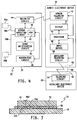
- the sensing portion 14 of the substrate 12 includes a sensor in the form of at least one working electrode 18A and at least one auxiliary electrode 18B formed thereon adjacent to an insertion tip 15 of the sensing portion 14.
- the auxiliary electrode 18B may be, depending upon the application, part of the working electrode 18A, another working electrode separate from the working electrode 18A, a counter electrode or a reference electrode. It will be understood that the sensor 18A,B may alternatively include additional or fewer electrodes formed on any side of the sensing portion 14 of the substrate 12, and that any such sensor electrodes may be located anywhere along the sensing portion 14. Alternatively still, the auxiliary electrode 18B and/or one or more additional electrodes associated with the sensor 18A,B may be formed on a different structure that is implanted within, inserted into or otherwise in contact with the patient.
- the sensor electrodes 18A and 18B are formed using electrically conductive traces 20A and 20B respectively that are disposed on the substrate 12 in a conventional manner.
- a sensing layer may be formed on, over or near either electrode 18A or 18B, or on, over or near both electrodes 18A and 18B, and in the illustrated embodiment a sensing layer 24A is formed over the electrode 18A.
- the sensing end 15 of the sensing portion 14 may be configured, as illustrated in FIGS. 1A and 2 , to facilitate percutaneous insertion of the sensing portion 14 into a patient.
- the substrate 12 may be formed using any one or combination of conventional, electrically non-conducting materials that are by themselves, or that may be further processed to be, suitable for in-vivo use.
- the substrate 12 is flexible, and in one specific embodiment the substrate 12 is made of Melinex® polyester film (e.g., polyethylene terephthalate).
- Suitable materials for a flexible substrate 12 include, for example, but are not limited to, electrically insulating plastic or polymeric materials such as polycarbonates, other polyesters such as Mylar®, polyvinyl chloride, polyurethanes, polyethers, polyimides, or copolymers of thermoplastics, such as glycol-modified polyethylene terephthalate, and/or other electrically non-conducting, flexible, deformable materials.
- the substrate 12 is rigid, and may be made using conventional electrically non-conducting materials. Examples of such rigid, electrically non-conducting materials include, but are not limited to, ceramics, such as aluminum oxide and silicon dioxide, and the like. Combinations of flexible and non-flexible materials are also contemplated.
- films of carbon, conductive polymer, metal, alloy, or metallic compound are well-known and include, for example, but are not limited to, chemical vapor deposition (CVD), physical vapor deposition, sputtering, reactive sputtering, printing, coating, and painting.
- CVD chemical vapor deposition
- the electrically conductive pads, e.g., 22A and 22B may, but need not, be formed of the same material used to form the electrically conductive traces, e.g., 20A and 20B.
- the one or more electrically conductive pads e.g., pads 22A and 22B on the circuit mounting portion 16 of the substrate 12 and/or by suitably positioning the one or more electrical terminals on the electrical circuit 32 so that one or more of the electrical terminals align with one or more of the electrically conductive pads when the circuit 32 is juxtaposed over the circuit mounting portion 16 of the substrate 12, local electrical contact is established therebetween when the components 16, 30 and 32 are assembled as illustrated in FIGS. 2 and 3 .
- the anisotropic medium 30 may be provided in the form of a conventional anisotropic electrically conductive adhesive tape.
- the tape in this embodiment is a flexible adhesive matrix filled with electrically conductive particles that provide electrical connectivity in a direction through the plane of the tape, but which are spaced sufficiently far apart so that the tape is electrically insulating in directions along the plane of the tape.
- the anisotropic adhesive tape 30 is disposed between the circuit mounting portion 16 of the substrate 12 and the electrical circuit 32, as shown in FIGS. 2 and 3 .
- the elastomer 30 defines a plane generally parallel to opposing surfaces of the electrical circuit 32 and the circuit mounting portion 16 of the substrate 12, and the elastomer 30 is electrically insulating in directions along or parallel to the plane and electrically conductive in a direction generally perpendicular to the plane.
- the sensor control circuit 32 may illustratively include a conventional telemetry circuit 44 that is electrically connected to the sensor operating circuit 42.
- the telemetry circuit 44 may be configured to wirelessly transmit signals to a remote electronic device 50, and/or to receive signals from the remote electronic device 50.
- the telemetry circuit 44 may be controlled by the sensor operating circuit 40 to transmit and/or receive specified information, or may alternatively be controlled by the sensor operating circuit 40 only to transmit information and to be responsive to signals transmitted by the remote electronic device 50 to receive information.
- the telemetry circuit 44 may be configured to conduct wireless communication using any conventional wireless communication techniques. Examples of such conventional wireless communications techniques include, but are not limited to, infrared (IR) communications, radio frequency (RF) communications, inductively coupled communications, or the like.
- the sensor control circuit 32 may also illustratively include a conventional event notification circuit 46 that is electrically connected to the sensor operating circuit 42.
- the event notification circuit 46 is configured to provide a notification of a specified event, and may accordingly include any one or more conventional visual, audible and/or tactile indication devices.
- the event notification circuit 46 is configured to be responsive to an event notification signal to activate the one or more visual, audible and/or tactile indication devices according to any desired indication pattern.
- the event that triggers activation of the one or more visual, audible and/or tactile indication devices of the event notification circuit 46 generally results from information provided by the sensor 18A, 18B.
- the sensor control circuit 32 may be implemented in any of a variety of conventional forms.
- the sensor control circuit 32 may be a single, monolithic integrated circuit configured to include at least the sensor operating circuit 40, and to optionally include any one or more of the telemetry circuit 44, the event notification circuit 46 and the acknowledgement circuit 48.
- the one or more electrical terminals comprise one or more electrically conductive circuit terminals or leads extending from a hermetically sealed integrated circuit package containing the integrated circuit.
- the structure 33 thus represents a packaged integrated circuit.
- the sensor operating circuit 40 and optionally any one or more of the telemetry circuit 44, the event notification circuit 46 and the acknowledgement circuit 48, is mounted to a top side of the substrate 33, and the one or more electrical terminals defined on the underside of the substrate 33 are electrically connected to corresponding electrical terminals or circuit traces defined on the top side of the substrate 33 in a conventional manner.
- An example of this is illustrated in FIG. 3 where the electrical terminal 34A defined on the bottom surface of the sensor control circuit 32 is electrically connected via an electrical conductor 35 to an electrical terminal 34A' defined on the top surface of the sensor control circuit 32.
- the two electrical terminals 34A and 34A' may be electrically connected using conventional techniques including, for example, but not limited to, plated-though hole technology, using multiple layers of conductors interconnected by vias, wrapping electrically conductive circuit traces around the substrate from the top surface to the bottom surface, and the like.
- suitable flexible materials that may be used to implement the substrate 33 in flexible form include, but are not limited to, Melinex® polyester film (e.g., polyethylene terephthalate), other polyesters such as Mylar®, polyvinyl chloride, electrically insulating plastic or polymeric materials such as polycarbonates, polyurethanes, polyethers, polyimides, or copolymers of thermoplastics, such as glycol-modified polyethylene terephthalate, and/or other electrically non-conducting, flexible, deformable materials.
- suitable rigid materials that may be used to implement the substrate 33 in rigid form include, but are not limited to, ceramics, such as aluminum oxide and silicon dioxide, conventional printed circuit boards, conventional multi-layer printed circuit boards, and the like. Combinations of flexible and non-flexible materials are also contemplated.
- a remote electronic device 50 may include a sensor telemetry circuit 52 configured to wirelessly transmit signals to and/or receive signals from the telemetry circuit 44 of the sensor control circuit 32.
- the remote electronic device 50 may further include a conventional processor circuit 54, which may be implemented in the form of a conventional microprocessor that is electrically connected to the sensor telemetry circuit 52 and to an input device 56.
- An input device 56 may be or include a keyboard, key pad, touch screen display device, voice-activated device or the like, and may be used in a conventional manner to supply the processor 54 with information that may include, for example, commands to execute a desired function or process.
- a conventional display 57 may be included as part of the electronic device 50, and may be controlled by the processor 54 in a conventional manner to display messages, alerts and/or warnings in the form of one or more of a visual, audible or tactile form.
- the sensor operating circuit 40 of the electrical circuit 36 is operable to control the telemetry circuit 44 to transmit a wireless event signal, as described hereinabove
- the telemetry circuit 52 of the electronic device 50 is operable to receive the wireless event signal and provide this signal to the processor 54.
- the processor 54 is, in turn, responsive to the wireless event signal to activate the display 57 to display, in visual, audible and/or tactile form, an indicator of the event.
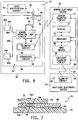
- the intermediate substrate 80 defines therethrough two such passageways 82A and 82B that align with corresponding electrically conductive pads 22A and 22B defined on the circuit mounting portion 16 of the substrate 12, and that are juxtaposed over the corresponding electrically conductive pads 22A and 22B when the substrate 80 is mounted to the circuit mounting portion 16 of the substrate 12.
- the substrate 80 may be attached to the circuit mounting portion 16 of the substrate 12 via a conventional attachment medium, and in the embodiment illustrated in FIG. 7 the substrate 80 is shown being attached or mounted to the mounting portion 16 of the substrate 12 via a conventional adhesive 84.
- suitable attachment mechanisms include, but are not limited to, conventional epoxies or other formable or settable mediums, conventional adhesives including adhesive tapes, or the like.
- suitable flexible materials that may be used to implement the substrate 80 in flexible form include, but are not limited to, Melinex® polyester film (e.g., polyethylene terephthalate), other polyesters such as Mylar®, polyvinyl chloride, electrically insulating plastic or polymeric materials such as polycarbonates, polyurethanes, polyethers, polyimides, or copolymers of thermoplastics, such as glycol-modified polyethylene terephthalate, and/or other electrically non-conducting, flexible, deformable materials.
- suitable rigid materials that may be used to implement the substrate 80 in rigid form include, but are not limited to, ceramics, such as aluminum oxide and silicon dioxide, conventional printed circuit boards, conventional multi-layer printed circuit boards, and the like. Combinations of flexible and non-flexible materials are also contemplated.
- the one or more electrical terminals defined by the electrical circuit 32 also align with the one or more passageways defined through the intermediate substrate 80.
- the electrical terminals 34A and 34B align with the passageways 82A and 82B respectively so that the terminals 34A and 34B are juxtaposed over the electrically conductive pads 22A and 22B when the electrical circuit 32 is mounted to the intermediate substrate 80 and the intermediate substrate 80 is also mounted to the circuit mounting portion 16 of the substrate 12, as illustrated in FIGS. 6 and 7 .
- Electrical connection between the electrically conductive terminals 34A and 34B and the corresponding electrically conductive pads 22A and 22B respectively is made using conventional electrical interconnection techniques.
- Examples of such electrical interconnection techniques include, but are not limited to, curable solder paste, solder bumps, electrically conductive adhesive, an electrically conductive formable medium such as an electrically conductive resin, or the like.
- the electrical connection is shown as taking the form of a formable metallic conductor 86, e.g., solder, that forms an electrical and mechanical bond to the electrically conductive terminal 34A and to the electrically conductive pad 22A.
- This mechanical connection may serve also as the mechanical attachment mechanism for mounting the electrical circuit 32 to the intermediate substrate 80, as illustrated in FIG. 7 , or a conventional attachment medium may alternatively be used to attach or mount the electrical circuit 32 to the substrate 80.
- Examples of such conventional attachment mechanisms include, but are not limited to, conventional epoxies or other formable or settable mediums, conventional adhesives including adhesive tapes, or the like.
- the event notification circuit 46 is shown as being mounted to and carried by the substrate 80 while a remainder 32' of the sensor control circuitry 40, 43, 44 and 48 is mounted to a sensor control circuit substrate 88. It will be understood that in this embodiment, any one or more of the sensor control circuit components may be mounted to the substrate 80, and that the event notification circuit 46 is shown mounted to the substrate 80 only by way of example. In any case, any portion of the sensor control circuit 32 that is mounted to the substrate 80 is electrically connected to a remainder of the sensor control circuit 32' that is mounted to the sensor control circuit substrate 88 using conventional electrical connection structures and techniques.
- the substrate 88 defines an electrically conductive pad or terminal 90 on a top side of thereof that is electrically connected to the sensor operating circuit 40 via an electrically conductive trace 92.
- the substrate 80 likewise defines an electrically conductive pad or terminal 94 on the top side thereof that is electrically connected to the event notification circuit 46 via an electrically conductive trace 96.
- the electrically conductive pads or terminals 90 and 94 are electrically connected together in a conventional manner to electrically connect the event notification circuit 46 to the sensor operating circuit 40.
- the substrate 88 defines an electrically conductive pad 98 on the bottom surface thereof that aligns with, and is juxtaposed over, an electrically conductive pad 99 formed on the top surface of the substrate 80 when the substrate 88 is mounted to the substrate 80. Electrical interconnection therebetween may be made using conventional techniques, or by interposing an anisotropic electrically conductive medium, such as the anisotropic electrically conductive medium 30 illustrated and described hereinabove, between the substrates 80 and 88 at least between the electrically conductive pads 98 and 99.
- an anisotropic electrically conductive medium such as the anisotropic electrically conductive medium 30 illustrated and described hereinabove
- the sensor module 100 includes some of the same structural components as the sensor module 10 of FIGS. 1-4 , and like numbers are therefore used to identify like components.
- an intermediate substrate 110 is introduced between the circuit mounting portion 16 of the substrate 12 and an electrical circuit 132.
- the intermediate substrate 110 is flexible or in other examples rigid, and in either case the substrate 110 defines one or more electrically conductive pads on the bottom surface thereof that align with one or more of the number of electrically conductive pads defined on the circuit mounting portion 16 of the substrate 12 when the substrate 110 is mounted to the circuit mounting portion 16 of the substrate 12.
- the substrate 110 may be attached to the circuit mounting portion 16 of the substrate 12 via any conventional attachment medium, and electrical connections between the electrically conductive pads 22A and 112A and between the electrically conductive pads 22B and 112B may be established via any conventional electrical connection structure or technique.
- suitable flexible materials that may be used to implement the substrate 110 in flexible form include, but are not limited to, Melinex® polyester film (e.g., polyethylene terephthalate), other polyesters such as Mylar®, polyvinyl chloride, electrically insulating plastic or polymeric materials such as polycarbonates, polyurethanes, polyethers, polyimides, or copolymers of thermoplastics, such as glycol-modified polyethylene terephthalate, and/or other electrically non-conducting, flexible, deformable materials.
- suitable rigid materials that may be used to implement the substrate 110 in rigid form include, but are not limited to, ceramics, such as aluminum oxide and silicon dioxide, conventional printed circuit boards, conventional multi-layer printed circuit boards, and the like. Combinations of flexible and non-flexible materials are also contemplated.
- the substrate 110 also defines a number of electrically conductive pads on the top surface thereof, at least some of which are electrically connected to corresponding electrically conductive pads defined on the bottom surface of the substrate 110, and one or more of which align with a corresponding one or more electrically conductive pads defined on the bottom surface of the electrical circuit 132 when the electrical circuit 132 is mounted to the substrate 110.
- a pair of electrically conductive pads 114A and 114B are defined on the top surface of the substrate 110.
- the electrically conductive pad 114A defined on the top surface of the substrate 110 is electrically connected to the electrically conductive pad 112A defined on the bottom surface of the substrate 110 by an electrical conductor or electrically conductive trace 116A, and the electrically conductive pad 114B defined on the top surface of the substrate 110 is likewise electrically connected to the electrically conductive pad 112B defined on the bottom surface of the substrate 110 by an electrical conductor or electrically conductive trace 116B.
- the electrical conductors or electrically conductive traces 116A and 116B may be formed using conventional electrical connection technology, examples of which include, but are not limited to, plated-though hole technology, using multiple layers of conductors interconnected by vias, wrapping electrically conductive circuit traces around the substrate from the top surface to the bottom surface, and the like.
- the electrical circuit 132 may take any of the forms described hereinabove with respect to the description of the electrical circuit 32, and may be configured as described hereinabove to communicate with a remote electronic device 50.
- the device 50 may also be configured to communicate with an auxiliary electronic device 62. Details of the remote electronic device 50, the auxiliary electronic device 62 and operation thereof are provided hereinabove.
- the sensor operating circuit 40 is mounted to a top surface of a rigid or in other examples flexible substrate 133 that is attached to the substrate 110 as described hereinabove with respect to FIGS. 11A or 11B .
- the sensor operating circuit 40 has a first input that is electrically connected to the electrically conductive pad 134A via an electrical conductor or electrically conductive trace 138A, and a second input that is electrically connected to the electrically conductive pad 134B via an electrical conductor or electrically conductive trace 138B.
- a telemetry circuit 44, an event notification circuit 46 and/or an acknowledge circuit 48 may also be mounted to the substrate 133 and electrically interconnected as described hereinabove.
- the sensor operating circuit 40 and optionally any one or more of the telemetry circuit 44, the event notification circuit 46 and the acknowledgement circuit 48, is mounted to a top side of the substrate 133, and the one or more electrical terminals defined on the bottom surface of the substrate 133 are electrically connected to corresponding electrical terminals or circuit traces defined on the top side of the substrate 33 in a conventional manner.
- FIGS. 11A and 11B where the electrical terminal 134B defined on the bottom surface of the sensor control circuit 32 is electrically connected via an electrical conductor 135 to an electrical terminal 134B' defined on the top surface of the sensor control circuit 32.
- a portion 132' of the electrical circuit 132 may be mounted to a modified substrate 133' that is itself attached to a modified substrate 110', and a remainder of the electrical circuit 132 may be mounted to and carried by the substrate 110'.
- the telemetry circuit 44 is shown as being mounted to and carried by the substrate 110' while a remainder 132' of the sensor control circuitry 40, 42, 46 and 48 is mounted to the substrate 133'. It will be understood that in this embodiment, any one or more of the sensor control circuit components may be mounted to the substrate 110', and that the telemetry circuit 44 is shown mounted to the substrate 110' only by way of example.
- any portion of the sensor control circuit 132 that is mounted to the substrate 110' is electrically connected to a remainder of the sensor control circuit 132' that is mounted to the substrate 133' using conventional electrical connection structures and techniques.
- the substrate 110' is modified, relative to the substrate 110 of FIG. 12 , to define an electrically conductive pad 114C on a top side of thereof that is electrically connected to the telemetry circuit 44 via an electrically conductive trace 116C.
- the substrate 133' is likewise modified, relative to the substrate 133, to define an electrically conductive pad 134C on the bottom surface thereof that is electrically connected to an input of the sensor operating circuit 40 via an electrically conductive trace 138C.
- the substrate 110" is modified, relative to the substrates 110 and 110' of FIGS. 12 and 13 respectively, to define a number of electrically conductive terminals 114A', 114B' and 114C' in place of the electrically conductive pads 114A, 114B and 114C, that may or may not be implemented in the form of electrically conductive pads, that may be defined on the top or bottom surface of the substrate 110" and that may or may not align with corresponding electrical terminals defined on the modified substrate 133".
- suitable flexible materials that may be used to implement the substrates 110, 110', 110", 133, 133' and 133" in flexible form include, but are not limited to, Melinex® polyester film (e.g., polyethylene terephthalate), other polyesters such as Mylar®, polyvinyl chloride, electrically insulating plastic or polymeric materials such as polycarbonates, polyurethanes, polyethers, polyimides, or copolymers of thermoplastics, such as glycol-modified polyethylene terephthalate, and/or other electrically non-conducting, flexible, deformable materials.
- Melinex® polyester film e.g., polyethylene terephthalate
- other polyesters such as Mylar®
- polyvinyl chloride polyvinyl chloride
- electrically insulating plastic or polymeric materials such as polycarbonates, polyurethanes, polyethers, polyimides, or copolymers of thermoplastics, such as glycol-modified polyethylene terephthalate,
- suitable rigid materials that may be used to implement the substrates 110, 110', 110", 133, 133' and 133" in rigid form include, but are not limited to, ceramics, such as aluminum oxide and silicon dioxide, conventional printed circuit boards, conventional multi-layer printed circuit boards, and the like. Combinations of flexible and non-flexible materials are also contemplated.
- the telemetry circuit 44 may be mounted to and carried by the substrate 133 or 133' while the remainder 132' of the sensor control circuitry 40, 43, 44 and/or 46 is mounted to and carried by the substrate 110, 110' or 110".
- the telemetry circuit 44 is electrically connected to a remainder of the sensor control circuit 132' that is mounted to the substrate 110, 110' or 110" using conventional electrical connection structures and techniques of the type just described.
Landscapes
- Health & Medical Sciences (AREA)
- Life Sciences & Earth Sciences (AREA)
- Engineering & Computer Science (AREA)
- Physics & Mathematics (AREA)
- Molecular Biology (AREA)
- Surgery (AREA)
- Veterinary Medicine (AREA)
- Public Health (AREA)
- General Health & Medical Sciences (AREA)
- Biophysics (AREA)
- Pathology (AREA)
- Biomedical Technology (AREA)
- Heart & Thoracic Surgery (AREA)
- Medical Informatics (AREA)
- Animal Behavior & Ethology (AREA)
- Microelectronics & Electronic Packaging (AREA)
- General Chemical & Material Sciences (AREA)
- Chemical & Material Sciences (AREA)
- Chemical Kinetics & Catalysis (AREA)
- Optics & Photonics (AREA)
- Manufacturing & Machinery (AREA)
- Computer Networks & Wireless Communication (AREA)
- Physiology (AREA)
- Nuclear Medicine, Radiotherapy & Molecular Imaging (AREA)
- Radiology & Medical Imaging (AREA)
- Measuring And Recording Apparatus For Diagnosis (AREA)
- Arrangements For Transmission Of Measured Signals (AREA)
- Measurement And Recording Of Electrical Phenomena And Electrical Characteristics Of The Living Body (AREA)
Claims (15)
- Sensor (70), umfassend:ein erstes Substrat (12), das einen Erfassungsabschnitt (14), der konfiguriert ist, perkutan in einen Patienten eingeführt zu werden, und einen extrakorporalen Schaltkreismontageabschnitt (16) aufweist, wobei auf dem Erfassungsabschnitt (14) ein Sensor (18A, 18B) definiert ist und wobei auf dem Schaltkreismontageabschnitt (16) mindestens eine elektrisch leitfähige Kontaktstelle (22A, 22B) definiert ist, die mit dem Sensor elektrisch verbunden ist, wobei der Sensor (18A, 18B) konfiguriert ist, um ein Signal zu produzieren, das einen Patientenzustand anzeigt,gekennzeichnet durchein zweites Substrat (80, 110), das an dem ersten Substrat (12) angebracht ist und auf dem eine erste Anzahl von elektrisch leitfähigen Kontaktstellen (34A, 34B, 99; 112A, 112B, 114A, 114B) definiert ist, wobei mindestens eine aus der ersten Anzahl von elektrisch leitfähigen Kontaktstellen ausgerichtet ist auf die mindestens eine elektrisch leitfähige Kontaktstelle, die auf dem ersten Substrat (12) definiert ist, und wobei mindestens eine weitere aus der ersten Anzahl von elektrisch leitfähigen Kontaktstellen, die auf dem zweiten Substrat (80, 110) definiert ist, mit der mindestens einen aus der ersten Anzahl von elektrisch leitfähigen Kontaktstellen elektrisch verbunden ist, die auf dem zweiten Substrat (80, 110) definiert ist,ein Element zum Einrichten eines elektrischen Kontakts zwischen der mindestens einen elektrisch leitfähigen Kontaktstelle, die auf dem ersten Substrat (12) definiert ist, und der mindestens einen aus der ersten Anzahl von elektrisch leitfähigen Kontaktstellen, die auf dem zweiten Substrat definiert ist,ein drittes Substrat (88, 133), das an dem zweiten Substrat (80, 110) angebracht ist und auf dem die mindestens einen elektrischen Anschluss (98, 134) definiert ist,eine erste Anzahl von elektrischen Komponenten (40, 43, 44, 46, 48), die an dem dritten Substrat angebracht ist, und eine zweite Anzahl von elektrischen Komponenten (40, 43, 44, 46, 48), die an dem zweiten Substrat (80, 110) angebracht ist, wobei die zweite Anzahl von elektrischen Komponenten (40, 43, 44, 46, 48) und die erste Anzahl von elektrischen Komponenten (40, 43, 44, 46, 48) zusammen einen Sensorsteuerschaltkreis (32, 132) bilden, wobei der Sensorsteuerschaltkreis (32, 132) mit dem mindestens einen elektrischen Anschluss (98, 134) elektrisch verbunden ist, die auf dem dritten Substrat (88, 133) definiert ist, undein Element zum Einrichten eines elektrischen Kontakts zwischen der mindestens einen weiteren aus der ersten Anzahl von elektrisch leitfähigen Kontaktstellen, die auf dem zweiten Substrat (80, 110) definiert ist, und dem mindestens einen elektrischen Anschluss, die auf dem dritten Substrat (88, 133) definiert ist, wodurch der Sensor (18A, 18B) mit dem Sensorsteuerschaltkreis (32, 132) elektrisch verbunden wird;wobei das zweite Substrat (80, 110) flexibel ist und das dritte Substrat (88, 133) starr ist.
- Sensor nach Anspruch 1, wobei der Sensorsteuerschaltkreis (32, 132) einen Telemetrieschaltkreis (44) umfasst, der konfiguriert ist, um Kommunikationssignale an eine ferne elektronische Vorrichtung (50) zu senden oder von ihr zu empfangen.
- Sensor nach Anspruch 1, wobei der Sensorsteuerschaltkreis (32, 132) einen Benachrichtigungsschaltkreis (46) umfasst, der konfiguriert ist, um eine optische, akustische und fühlbare Anzeige eines vordefinierten Ereignisses zu erzeugen.
- Sensor nach Anspruch 3, wobei der Sensorsteuerschaltkreis (32, 132) einen Bestätigungsschaltkreis (48) umfasst, der auf eine Benutzeraktivierung desselben reagiert, um das Erzeugen der optischen, akustischen oder fühlbaren Anzeige des vordefinierten Ereignisses zu bestätigen.
- Sensor nach Anspruch 1, der außerdem umfasstein Element zum elektrischen Verbinden der zweiten Anzahl von elektrischen Komponenten mit der ersten Anzahl von elektrischen Komponenten.
- Sensor nach Anspruch 5, wobei die zweite Anzahl von elektrischen Komponenten einen Sensorbetriebsschaltkreis (40) umfasst, der konfiguriert ist, den Sensor zu betreiben.
- Sensor nach Anspruch 1, wobei auf dem Schaltkreismontageabschnitt (16) des ersten Substrats (12) eine zweite Anzahl von elektrisch leitfähigen Kontaktstellen definiert ist,
und wobei mindestens einige der ersten Anzahl von elektrisch leitfähigen Kontaktstellen, die auf dem zweiten Substrat (80, 110) definiert ist, auf entsprechende Kontaktstellen der zweiten Anzahl von elektrisch leitfähigen Kontaktstellen ausgerichtet sind, die auf dem Schaltkreismontageabschnitt (16) des ersten Substrats (12) definiert ist, wenn das zweite Substrat (80, 110) an dem ersten Substrat (12) angebracht ist. - Sensor nach Anspruch 7, wobei auf dem dritten Substrat eine dritte Anzahl von elektrischen Anschlüssen definiert ist,
und wobei mindestens einige andere der ersten Anzahl von elektrisch leitfähigen Kontaktstellen, die auf dem zweiten Substrat (80, 110) definiert ist, auf entsprechende Anschlüsse der dritten Anzahl von elektrischen Anschlüssen ausgerichtet sind, die auf dem dritten Substrat definiert ist. - Sensor nach Anspruch 7, wobei auf dem dritten Substrat (88, 133) eine dritte Anzahl von elektrischen Anschlüssen definiert ist,
und wobei das dritte Substrat außerdem ein Element zum elektrischen Verbinden von mindestens einigen anderen der ersten Anzahl von elektrisch leitfähigen Kontaktstellen, die auf dem zweiten Substrat (80, 110) definiert ist, mit entsprechenden Anschlüssen der dritten Anzahl von elektrischen Anschlüssen umfasst, die auf dem dem dritten Substrat (88, 133) definiert ist. - Sensor nach Anspruch 1, der außerdem eine erste Anzahl von elektrischen Komponenten, die an dem dritten Substrat (88, 133) angebracht ist, und eine zweite Anzahl von elektrischen Komponenten umfasst, die an dem zweiten Substrat (80, 110) angebracht ist, wobei die zweite Anzahl von elektrischen Komponenten und die erste Anzahl von elektrischen Komponenten zusammen den Sensorsteuerschaltkreis (32, 132) bilden, wobei der Sensorsteuerschaltkreis (32, 132) mit mindestens einem elektrischen Anschluss elektrisch verbunden ist.
- Sensor nach Anspruch 10, der außerdem ein Element zum elektrischen Verbinden der zweiten Anzahl von elektrischen Komponenten mit der ersten Anzahl von elektrischen Komponenten umfasst.
- Sensor nach Anspruch 11, wobei die zweite Anzahl von elektrischen Komponenten einen Sensorbetriebsschaltkreis (40) umfasst, der konfiguriert ist, den Sensor zu betreiben.
- Sensor nach Anspruch 11, wobei die zweite Anzahl von elektrischen Komponenten einen Telemetrieschaltkreis (44) umfasst, der konfiguriert ist, um Kommunikationssignale an eine ferne elektronische Vorrichtung zu senden oder von ihr zu empfangen.
- Sensor nach Anspruch 11, wobei die zweite Anzahl von elektrischen Komponenten einen Benachrichtigungsschaltkreis (46) umfasst, der konfiguriert ist, um eine optische, akustische oder fühlbare Anzeige eines vordefinierten Ereignisses zu erzeugen.
- Sensor nach Anspruch 11, wobei die zweite Anzahl von elektrischen Komponenten einen Bestätigungsschaltkreis (48) umfasst, der auf eine Benutzeraktivierung desselben reagiert, um das Erzeugen der optischen, akustischen oder fühlbaren Anzeige des vordefinierten Ereignisses zu bestätigen.
Priority Applications (3)
| Application Number | Priority Date | Filing Date | Title |
|---|---|---|---|
| PL08749252T PL2152147T3 (pl) | 2007-05-01 | 2008-04-30 | Czujnik do monitorowania stanu pacjenta |
| SI200831878T SI2152147T1 (sl) | 2007-05-01 | 2008-04-30 | Tipalo za spremljanje stanja pacienta |
| EP17162571.8A EP3202312B1 (de) | 2007-05-01 | 2008-04-30 | Sensor zur überwachung eines patientenzustandes |
Applications Claiming Priority (2)
| Application Number | Priority Date | Filing Date | Title |
|---|---|---|---|
| US11/742,998 US20080275326A1 (en) | 2007-05-01 | 2007-05-01 | Sensor for monitoring a condition of a patient |
| PCT/EP2008/003505 WO2008131963A1 (en) | 2007-05-01 | 2008-04-30 | Sensor for monitoring a condition of a patient |
Related Child Applications (2)
| Application Number | Title | Priority Date | Filing Date |
|---|---|---|---|
| EP17162571.8A Division-Into EP3202312B1 (de) | 2007-05-01 | 2008-04-30 | Sensor zur überwachung eines patientenzustandes |
| EP17162571.8A Division EP3202312B1 (de) | 2007-05-01 | 2008-04-30 | Sensor zur überwachung eines patientenzustandes |
Publications (2)
| Publication Number | Publication Date |
|---|---|
| EP2152147A1 EP2152147A1 (de) | 2010-02-17 |
| EP2152147B1 true EP2152147B1 (de) | 2017-08-23 |
Family
ID=39592000
Family Applications (2)
| Application Number | Title | Priority Date | Filing Date |
|---|---|---|---|
| EP17162571.8A Active EP3202312B1 (de) | 2007-05-01 | 2008-04-30 | Sensor zur überwachung eines patientenzustandes |
| EP08749252.6A Active EP2152147B1 (de) | 2007-05-01 | 2008-04-30 | Sensor zur überwachung eines patientenzustands |
Family Applications Before (1)
| Application Number | Title | Priority Date | Filing Date |
|---|---|---|---|
| EP17162571.8A Active EP3202312B1 (de) | 2007-05-01 | 2008-04-30 | Sensor zur überwachung eines patientenzustandes |
Country Status (9)
| Country | Link |
|---|---|
| US (3) | US20080275326A1 (de) |
| EP (2) | EP3202312B1 (de) |
| DK (1) | DK2152147T3 (de) |
| ES (1) | ES2978936T3 (de) |
| HU (1) | HUE067251T2 (de) |
| NO (1) | NO2152147T3 (de) |
| PL (1) | PL2152147T3 (de) |
| SI (1) | SI2152147T1 (de) |
| WO (1) | WO2008131963A1 (de) |
Families Citing this family (20)
| Publication number | Priority date | Publication date | Assignee | Title |
|---|---|---|---|---|
| US7920906B2 (en) | 2005-03-10 | 2011-04-05 | Dexcom, Inc. | System and methods for processing analyte sensor data for sensor calibration |
| US9247900B2 (en) | 2004-07-13 | 2016-02-02 | Dexcom, Inc. | Analyte sensor |
| US8989833B2 (en) | 2004-07-13 | 2015-03-24 | Dexcom, Inc. | Transcutaneous analyte sensor |
| US8133178B2 (en) | 2006-02-22 | 2012-03-13 | Dexcom, Inc. | Analyte sensor |
| US20090076360A1 (en) | 2007-09-13 | 2009-03-19 | Dexcom, Inc. | Transcutaneous analyte sensor |
| KR101088806B1 (ko) * | 2009-01-07 | 2011-12-01 | 주식회사 뉴로바이오시스 | 액정 폴리머를 이용한 미세 전극 어레이 패키지 및 그의 제조 방법 |
| JP2013522588A (ja) | 2010-03-12 | 2013-06-13 | エンハンスド サーフェイス ダイナミクス,インコーポレイテッド | 圧力感知システム内の圧力センサからデータを高速収集するシステム及び方法 |
| RU2014102675A (ru) | 2011-07-13 | 2015-08-20 | Энхэнсд Сёрфейс Дайнэмикс, Инк. | Способы и системы изготовления и включения мата обнаружения давления |
| US8726496B2 (en) | 2011-09-22 | 2014-05-20 | Covidien Lp | Technique for remanufacturing a medical sensor |
| US8692992B2 (en) * | 2011-09-22 | 2014-04-08 | Covidien Lp | Faraday shield integrated into sensor bandage |
| ES2759560T3 (es) * | 2012-06-28 | 2020-05-11 | Hoffmann La Roche | Dispositivo de monitorización de al menos una función corporal de un usuario y procedimiento de fabricación del mismo |
| ES2970374T3 (es) * | 2012-06-29 | 2024-05-28 | Hoffmann La Roche | Elemento sensor para detectar un analito en un líquido corporal |
| KR20160028356A (ko) * | 2014-09-03 | 2016-03-11 | 크루셜텍 (주) | 지문센서 모듈 및 이의 제조방법 |
| US10492734B2 (en) | 2016-11-04 | 2019-12-03 | Wellsense, Inc. | Patient visualization system |
| US11083418B2 (en) | 2016-11-04 | 2021-08-10 | Wellsense, Inc. | Patient visualization system |
| US10612078B2 (en) * | 2017-02-13 | 2020-04-07 | California Institute Of Technology | Integrated electrochemical nucleic acid based sensors and related platforms |
| JP6718183B1 (ja) * | 2019-06-24 | 2020-07-08 | 株式会社アイ・メデックス | 電子回路基板を備えた生体電極 |
| US20220133184A1 (en) * | 2020-10-30 | 2022-05-05 | Medtronic Minimed, Inc. | Low-profile wearable medical device |
| US20220266039A1 (en) * | 2021-02-24 | 2022-08-25 | Medtronic, Inc. | Medical device patient two-way communication based on sensed event |
| WO2025178614A1 (en) * | 2024-02-21 | 2025-08-28 | Roche Diabetes Care, Inc. | Continuous analyte monitor |
Family Cites Families (21)
| Publication number | Priority date | Publication date | Assignee | Title |
|---|---|---|---|---|
| US5482473A (en) * | 1994-05-09 | 1996-01-09 | Minimed Inc. | Flex circuit connector |
| US20050096513A1 (en) * | 1997-11-11 | 2005-05-05 | Irvine Sensors Corporation | Wearable biomonitor with flexible thinned integrated circuit |
| US6091975A (en) * | 1998-04-01 | 2000-07-18 | Alza Corporation | Minimally invasive detecting device |
| US6175752B1 (en) * | 1998-04-30 | 2001-01-16 | Therasense, Inc. | Analyte monitoring device and methods of use |
| US6248067B1 (en) * | 1999-02-05 | 2001-06-19 | Minimed Inc. | Analyte sensor and holter-type monitor system and method of using the same |
| US6554798B1 (en) * | 1998-08-18 | 2003-04-29 | Medtronic Minimed, Inc. | External infusion device with remote programming, bolus estimator and/or vibration alarm capabilities |
| US6565532B1 (en) * | 2000-07-12 | 2003-05-20 | The Procter & Gamble Company | Microneedle apparatus used for marking skin and for dispensing semi-permanent subcutaneous makeup |
| JP2002184487A (ja) * | 2000-12-15 | 2002-06-28 | Sony Chem Corp | 異方性導電接着剤 |
| US6560471B1 (en) * | 2001-01-02 | 2003-05-06 | Therasense, Inc. | Analyte monitoring device and methods of use |
| US7310543B2 (en) * | 2001-03-26 | 2007-12-18 | Kumetrix, Inc. | Silicon microprobe with integrated biosensor |
| US7204823B2 (en) * | 2001-12-19 | 2007-04-17 | Medtronic Minimed, Inc. | Medication delivery system and monitor |
| US6661161B1 (en) * | 2002-06-27 | 2003-12-09 | Andromed Inc. | Piezoelectric biological sound monitor with printed circuit board |
| US7278983B2 (en) * | 2002-07-24 | 2007-10-09 | Medtronic Minimed, Inc. | Physiological monitoring device for controlling a medication infusion device |
| KR100780136B1 (ko) * | 2002-11-29 | 2007-11-28 | 히다치 가세고교 가부시끼가이샤 | 접착제조성물 |
| WO2005084534A1 (en) * | 2003-09-03 | 2005-09-15 | Life Patch International, Inc. | Personal diagnostic devices and related methods |
| US8394328B2 (en) * | 2003-12-31 | 2013-03-12 | Nipro Diagnostics, Inc. | Test strip container with integrated meter having strip coding capability |
| US7299081B2 (en) * | 2004-06-15 | 2007-11-20 | Abbott Laboratories | Analyte test device |
| US7905833B2 (en) * | 2004-07-13 | 2011-03-15 | Dexcom, Inc. | Transcutaneous analyte sensor |
| EP2260759B1 (de) * | 2005-06-17 | 2015-05-06 | F. Hoffmann-La Roche AG | Sensorsystem sowie Anordnung und Verfahren zur Überwachung eines Inhaltsstoffs, insbesondere Glucose in Körpergewebe |
| US20070060869A1 (en) * | 2005-08-16 | 2007-03-15 | Tolle Mike C V | Controller device for an infusion pump |
| US20070060870A1 (en) * | 2005-08-16 | 2007-03-15 | Tolle Mike Charles V | Controller device for an infusion pump |
-
2007
- 2007-05-01 US US11/742,998 patent/US20080275326A1/en not_active Abandoned
-
2008
- 2008-04-30 PL PL08749252T patent/PL2152147T3/pl unknown
- 2008-04-30 NO NO08749252A patent/NO2152147T3/no unknown
- 2008-04-30 ES ES17162571T patent/ES2978936T3/es active Active
- 2008-04-30 WO PCT/EP2008/003505 patent/WO2008131963A1/en not_active Ceased
- 2008-04-30 EP EP17162571.8A patent/EP3202312B1/de active Active
- 2008-04-30 HU HUE17162571A patent/HUE067251T2/hu unknown
- 2008-04-30 DK DK08749252.6T patent/DK2152147T3/en active
- 2008-04-30 SI SI200831878T patent/SI2152147T1/sl unknown
- 2008-04-30 EP EP08749252.6A patent/EP2152147B1/de active Active
-
2013
- 2013-01-11 US US13/739,189 patent/US9579036B2/en active Active
-
2017
- 2017-02-08 US US15/427,741 patent/US20170181651A1/en not_active Abandoned
Non-Patent Citations (1)
| Title |
|---|
| None * |
Also Published As
| Publication number | Publication date |
|---|---|
| WO2008131963A1 (en) | 2008-11-06 |
| US9579036B2 (en) | 2017-02-28 |
| EP2152147A1 (de) | 2010-02-17 |
| PL2152147T3 (pl) | 2018-01-31 |
| US20140066737A1 (en) | 2014-03-06 |
| EP3202312B1 (de) | 2024-04-10 |
| ES2978936T3 (es) | 2024-09-23 |
| DK2152147T3 (en) | 2017-10-30 |
| US20080275326A1 (en) | 2008-11-06 |
| EP3202312A1 (de) | 2017-08-09 |
| EP3202312C0 (de) | 2024-04-10 |
| US20170181651A1 (en) | 2017-06-29 |
| SI2152147T1 (sl) | 2017-11-30 |
| HUE067251T2 (hu) | 2024-10-28 |
| NO2152147T3 (de) | 2018-01-20 |
Similar Documents
| Publication | Publication Date | Title |
|---|---|---|
| EP2152147B1 (de) | Sensor zur überwachung eines patientenzustands | |
| US7080560B2 (en) | Semiconductor pressure sensor | |
| US10076025B2 (en) | Stretchable circuit board and method for manufacturing the same | |
| US20040130528A1 (en) | Miniature highly manufacturable mouse pointing device | |
| KR20040105705A (ko) | 소형 및 대형 부품을 갖는 장치 및 그 장치의 제조 방법 | |
| US11406759B2 (en) | Method and devices for pressure determination in an insulin pump | |
| US20210239544A1 (en) | Earphone with force sensor | |
| KR20190052840A (ko) | 유연인쇄회로기판상 유연센서 접합방법, 및 유연센서가 접합된 유연센서인쇄회로기판 | |
| CN120303063A (zh) | 分析物监测设备 | |
| WO2009061154A1 (en) | Flexible tactile sensor module and method for manufacturing the same | |
| JP6718183B1 (ja) | 電子回路基板を備えた生体電極 | |
| KR20250080825A (ko) | 분석물 모니터링 장치 | |
| KR102813860B1 (ko) | 양면에 센서 패드가 형성된 연속식 분석물 측정기 | |
| US12484448B2 (en) | Deformation detection sensor | |
| JPH112617A (ja) | 結露センサ | |
| JP4665135B2 (ja) | バイオセンサーの製造法 | |
| CN220230764U (zh) | 一种薄膜式多点压力感测片及传感器 | |
| JP4670013B2 (ja) | バイオセンサーおよびその製造法 | |
| JP4974424B2 (ja) | 圧力検出装置用パッケージ | |
| CA3292149A1 (en) | Battery clip | |
| JPH0660853B2 (ja) | 圧覚センサ | |
| KR101065289B1 (ko) | 터치패널센서 및 터치패널센서의 제조방법 | |
| JP2020150148A (ja) | 集積回路基板、センシング装置、生体情報解析装置および集積回路基板の製造方法 | |
| JP2002350265A (ja) | 圧力検出装置用パッケージ | |
| JP2003065874A (ja) | 圧力検出装置用パッケージ |
Legal Events
| Date | Code | Title | Description |
|---|---|---|---|
| PUAI | Public reference made under article 153(3) epc to a published international application that has entered the european phase |
Free format text: ORIGINAL CODE: 0009012 |
|
| 17P | Request for examination filed |
Effective date: 20091201 |
|
| AK | Designated contracting states |
Kind code of ref document: A1 Designated state(s): AT BE BG CH CY CZ DE DK EE ES FI FR GB GR HR HU IE IS IT LI LT LU LV MC MT NL NO PL PT RO SE SI SK TR |
|
| AX | Request for extension of the european patent |
Extension state: AL BA MK RS |
|
| RIN1 | Information on inventor provided before grant (corrected) |
Inventor name: HAUETER, ULRICH Inventor name: KAMECKE, ULRIKE Inventor name: GRAY, STEVEN Inventor name: HINDELANG, FRITZ Inventor name: KASIELKE, TIMON Inventor name: LOUKINE, MICHAEL Inventor name: HOF, CHRISTIAN Inventor name: BUCK, HARVEY, B. Inventor name: KASIELKE, JOACHIM Inventor name: REYNOLDS, MATTHEW |
|
| DAX | Request for extension of the european patent (deleted) | ||
| 17Q | First examination report despatched |
Effective date: 20130502 |
|
| RAP1 | Party data changed (applicant data changed or rights of an application transferred) |
Owner name: ROCHE DIABETES CARE GMBH Owner name: F. HOFFMANN-LA ROCHE AG |
|
| GRAP | Despatch of communication of intention to grant a patent |
Free format text: ORIGINAL CODE: EPIDOSNIGR1 |
|
| INTG | Intention to grant announced |
Effective date: 20160920 |
|
| GRAJ | Information related to disapproval of communication of intention to grant by the applicant or resumption of examination proceedings by the epo deleted |
Free format text: ORIGINAL CODE: EPIDOSDIGR1 |
|
| STAA | Information on the status of an ep patent application or granted ep patent |
Free format text: STATUS: EXAMINATION IS IN PROGRESS |
|
| INTC | Intention to grant announced (deleted) | ||
| GRAP | Despatch of communication of intention to grant a patent |
Free format text: ORIGINAL CODE: EPIDOSNIGR1 |
|
| STAA | Information on the status of an ep patent application or granted ep patent |
Free format text: STATUS: GRANT OF PATENT IS INTENDED |
|
| INTG | Intention to grant announced |
Effective date: 20170323 |
|
| GRAS | Grant fee paid |
Free format text: ORIGINAL CODE: EPIDOSNIGR3 |
|
| GRAA | (expected) grant |
Free format text: ORIGINAL CODE: 0009210 |
|
| STAA | Information on the status of an ep patent application or granted ep patent |
Free format text: STATUS: THE PATENT HAS BEEN GRANTED |
|
| RIN1 | Information on inventor provided before grant (corrected) |
Inventor name: REYNOLDS, MATTHEW Inventor name: KAMECKE, ULRIKE Inventor name: GRAY, STEVEN Inventor name: LUKIN, MICHAEL Inventor name: KASIELKE, TIMON Inventor name: HINDELANG, FRITZ Inventor name: KASIELKE, JOACHIM Inventor name: BUCK, HARVEY, B. Inventor name: HAUETER, ULRICH Inventor name: HOF, CHRISTIAN |
|
| AK | Designated contracting states |
Kind code of ref document: B1 Designated state(s): AT BE BG CH CY CZ DE DK EE ES FI FR GB GR HR HU IE IS IT LI LT LU LV MC MT NL NO PL PT RO SE SI SK TR |
|
| REG | Reference to a national code |
Ref country code: GB Ref legal event code: FG4D |
|
| RIN1 | Information on inventor provided before grant (corrected) |
Inventor name: KASIELKE, TIMON Inventor name: HOF, CHRISTIAN Inventor name: GRAY, STEVEN Inventor name: REYNOLDS, MATTHEW Inventor name: KASIELKE, JOACHIM Inventor name: HINDELANG, FRITZ Inventor name: KAMECKE, ULRIKE Inventor name: BUCK, HARVEY, B. Inventor name: LUKIN, MICHAEL Inventor name: HAUETER, ULRICH |
|
| REG | Reference to a national code |
Ref country code: CH Ref legal event code: EP |
|
| REG | Reference to a national code |
Ref country code: AT Ref legal event code: REF Ref document number: 920398 Country of ref document: AT Kind code of ref document: T Effective date: 20170915 |
|
| REG | Reference to a national code |
Ref country code: IE Ref legal event code: FG4D |
|
| REG | Reference to a national code |
Ref country code: DE Ref legal event code: R096 Ref document number: 602008051755 Country of ref document: DE |
|
| REG | Reference to a national code |
Ref country code: NL Ref legal event code: FP |
|
| REG | Reference to a national code |
Ref country code: DK Ref legal event code: T3 Effective date: 20171024 |
|
| REG | Reference to a national code |
Ref country code: SE Ref legal event code: TRGR |
|
| REG | Reference to a national code |
Ref country code: NO Ref legal event code: T2 Effective date: 20170823 |
|
| REG | Reference to a national code |
Ref country code: LT Ref legal event code: MG4D |
|
| REG | Reference to a national code |
Ref country code: AT Ref legal event code: MK05 Ref document number: 920398 Country of ref document: AT Kind code of ref document: T Effective date: 20170823 |
|
| PG25 | Lapsed in a contracting state [announced via postgrant information from national office to epo] |
Ref country code: FI Free format text: LAPSE BECAUSE OF FAILURE TO SUBMIT A TRANSLATION OF THE DESCRIPTION OR TO PAY THE FEE WITHIN THE PRESCRIBED TIME-LIMIT Effective date: 20170823 Ref country code: LT Free format text: LAPSE BECAUSE OF FAILURE TO SUBMIT A TRANSLATION OF THE DESCRIPTION OR TO PAY THE FEE WITHIN THE PRESCRIBED TIME-LIMIT Effective date: 20170823 Ref country code: HR Free format text: LAPSE BECAUSE OF FAILURE TO SUBMIT A TRANSLATION OF THE DESCRIPTION OR TO PAY THE FEE WITHIN THE PRESCRIBED TIME-LIMIT Effective date: 20170823 Ref country code: AT Free format text: LAPSE BECAUSE OF FAILURE TO SUBMIT A TRANSLATION OF THE DESCRIPTION OR TO PAY THE FEE WITHIN THE PRESCRIBED TIME-LIMIT Effective date: 20170823 |
|
| PG25 | Lapsed in a contracting state [announced via postgrant information from national office to epo] |
Ref country code: ES Free format text: LAPSE BECAUSE OF FAILURE TO SUBMIT A TRANSLATION OF THE DESCRIPTION OR TO PAY THE FEE WITHIN THE PRESCRIBED TIME-LIMIT Effective date: 20170823 Ref country code: IS Free format text: LAPSE BECAUSE OF FAILURE TO SUBMIT A TRANSLATION OF THE DESCRIPTION OR TO PAY THE FEE WITHIN THE PRESCRIBED TIME-LIMIT Effective date: 20171223 Ref country code: LV Free format text: LAPSE BECAUSE OF FAILURE TO SUBMIT A TRANSLATION OF THE DESCRIPTION OR TO PAY THE FEE WITHIN THE PRESCRIBED TIME-LIMIT Effective date: 20170823 Ref country code: BG Free format text: LAPSE BECAUSE OF FAILURE TO SUBMIT A TRANSLATION OF THE DESCRIPTION OR TO PAY THE FEE WITHIN THE PRESCRIBED TIME-LIMIT Effective date: 20171123 Ref country code: GR Free format text: LAPSE BECAUSE OF FAILURE TO SUBMIT A TRANSLATION OF THE DESCRIPTION OR TO PAY THE FEE WITHIN THE PRESCRIBED TIME-LIMIT Effective date: 20171124 |
|
| REG | Reference to a national code |
Ref country code: FR Ref legal event code: PLFP Year of fee payment: 11 |
|
| PG25 | Lapsed in a contracting state [announced via postgrant information from national office to epo] |
Ref country code: RO Free format text: LAPSE BECAUSE OF FAILURE TO SUBMIT A TRANSLATION OF THE DESCRIPTION OR TO PAY THE FEE WITHIN THE PRESCRIBED TIME-LIMIT Effective date: 20170823 |
|
| REG | Reference to a national code |
Ref country code: DE Ref legal event code: R097 Ref document number: 602008051755 Country of ref document: DE |
|
| PG25 | Lapsed in a contracting state [announced via postgrant information from national office to epo] |
Ref country code: EE Free format text: LAPSE BECAUSE OF FAILURE TO SUBMIT A TRANSLATION OF THE DESCRIPTION OR TO PAY THE FEE WITHIN THE PRESCRIBED TIME-LIMIT Effective date: 20170823 Ref country code: SK Free format text: LAPSE BECAUSE OF FAILURE TO SUBMIT A TRANSLATION OF THE DESCRIPTION OR TO PAY THE FEE WITHIN THE PRESCRIBED TIME-LIMIT Effective date: 20170823 |
|
| PLBE | No opposition filed within time limit |
Free format text: ORIGINAL CODE: 0009261 |
|
| STAA | Information on the status of an ep patent application or granted ep patent |
Free format text: STATUS: NO OPPOSITION FILED WITHIN TIME LIMIT |
|
| 26N | No opposition filed |
Effective date: 20180524 |
|
| PG25 | Lapsed in a contracting state [announced via postgrant information from national office to epo] |
Ref country code: MC Free format text: LAPSE BECAUSE OF FAILURE TO SUBMIT A TRANSLATION OF THE DESCRIPTION OR TO PAY THE FEE WITHIN THE PRESCRIBED TIME-LIMIT Effective date: 20170823 |
|
| REG | Reference to a national code |
Ref country code: BE Ref legal event code: MM Effective date: 20180430 |
|
| REG | Reference to a national code |
Ref country code: IE Ref legal event code: MM4A |
|
| PG25 | Lapsed in a contracting state [announced via postgrant information from national office to epo] |
Ref country code: LU Free format text: LAPSE BECAUSE OF NON-PAYMENT OF DUE FEES Effective date: 20180430 |
|
| PG25 | Lapsed in a contracting state [announced via postgrant information from national office to epo] |
Ref country code: BE Free format text: LAPSE BECAUSE OF NON-PAYMENT OF DUE FEES Effective date: 20180430 |
|
| PG25 | Lapsed in a contracting state [announced via postgrant information from national office to epo] |
Ref country code: IE Free format text: LAPSE BECAUSE OF NON-PAYMENT OF DUE FEES Effective date: 20180430 |
|
| PG25 | Lapsed in a contracting state [announced via postgrant information from national office to epo] |
Ref country code: MT Free format text: LAPSE BECAUSE OF NON-PAYMENT OF DUE FEES Effective date: 20180430 |
|
| PG25 | Lapsed in a contracting state [announced via postgrant information from national office to epo] |
Ref country code: TR Free format text: LAPSE BECAUSE OF FAILURE TO SUBMIT A TRANSLATION OF THE DESCRIPTION OR TO PAY THE FEE WITHIN THE PRESCRIBED TIME-LIMIT Effective date: 20170823 |
|
| PG25 | Lapsed in a contracting state [announced via postgrant information from national office to epo] |
Ref country code: PT Free format text: LAPSE BECAUSE OF FAILURE TO SUBMIT A TRANSLATION OF THE DESCRIPTION OR TO PAY THE FEE WITHIN THE PRESCRIBED TIME-LIMIT Effective date: 20170823 Ref country code: HU Free format text: LAPSE BECAUSE OF FAILURE TO SUBMIT A TRANSLATION OF THE DESCRIPTION OR TO PAY THE FEE WITHIN THE PRESCRIBED TIME-LIMIT; INVALID AB INITIO Effective date: 20080430 |
|
| PG25 | Lapsed in a contracting state [announced via postgrant information from national office to epo] |
Ref country code: CY Free format text: LAPSE BECAUSE OF FAILURE TO SUBMIT A TRANSLATION OF THE DESCRIPTION OR TO PAY THE FEE WITHIN THE PRESCRIBED TIME-LIMIT Effective date: 20170823 |
|
| PGFP | Annual fee paid to national office [announced via postgrant information from national office to epo] |
Ref country code: NL Payment date: 20240320 Year of fee payment: 17 |
|
| PGFP | Annual fee paid to national office [announced via postgrant information from national office to epo] |
Ref country code: CZ Payment date: 20240326 Year of fee payment: 17 |
|
| PGFP | Annual fee paid to national office [announced via postgrant information from national office to epo] |
Ref country code: SE Payment date: 20240320 Year of fee payment: 17 Ref country code: PL Payment date: 20240325 Year of fee payment: 17 Ref country code: NO Payment date: 20240322 Year of fee payment: 17 Ref country code: IT Payment date: 20240320 Year of fee payment: 17 Ref country code: DK Payment date: 20240320 Year of fee payment: 17 |
|
| PGFP | Annual fee paid to national office [announced via postgrant information from national office to epo] |
Ref country code: CH Payment date: 20240501 Year of fee payment: 17 |
|
| PGFP | Annual fee paid to national office [announced via postgrant information from national office to epo] |
Ref country code: SI Payment date: 20240328 Year of fee payment: 17 |
|
| PGFP | Annual fee paid to national office [announced via postgrant information from national office to epo] |
Ref country code: DE Payment date: 20250319 Year of fee payment: 18 |
|
| REG | Reference to a national code |
Ref country code: DK Ref legal event code: EBP Effective date: 20250430 |
|
| REG | Reference to a national code |
Ref country code: CH Ref legal event code: H13 Free format text: ST27 STATUS EVENT CODE: U-0-0-H10-H13 (AS PROVIDED BY THE NATIONAL OFFICE) Effective date: 20251125 |
|
| REG | Reference to a national code |
Ref country code: NL Ref legal event code: MM Effective date: 20250501 |
|
| PG25 | Lapsed in a contracting state [announced via postgrant information from national office to epo] |
Ref country code: NO Free format text: LAPSE BECAUSE OF NON-PAYMENT OF DUE FEES Effective date: 20250430 |
|
| PG25 | Lapsed in a contracting state [announced via postgrant information from national office to epo] |
Ref country code: NL Free format text: LAPSE BECAUSE OF NON-PAYMENT OF DUE FEES Effective date: 20250501 |
|
| PG25 | Lapsed in a contracting state [announced via postgrant information from national office to epo] |
Ref country code: CH Free format text: LAPSE BECAUSE OF NON-PAYMENT OF DUE FEES Effective date: 20250430 |
|
| PG25 | Lapsed in a contracting state [announced via postgrant information from national office to epo] |
Ref country code: CZ Free format text: LAPSE BECAUSE OF NON-PAYMENT OF DUE FEES Effective date: 20250430 Ref country code: SE Free format text: LAPSE BECAUSE OF NON-PAYMENT OF DUE FEES Effective date: 20250501 |
|
| REG | Reference to a national code |
Ref country code: SE Ref legal event code: EUG |
|
| PGFP | Annual fee paid to national office [announced via postgrant information from national office to epo] |
Ref country code: GB Payment date: 20260319 Year of fee payment: 19 |
|
| PG25 | Lapsed in a contracting state [announced via postgrant information from national office to epo] |
Ref country code: DK Free format text: LAPSE BECAUSE OF NON-PAYMENT OF DUE FEES Effective date: 20250430 |
|
| PG25 | Lapsed in a contracting state [announced via postgrant information from national office to epo] |
Ref country code: IT Free format text: LAPSE BECAUSE OF NON-PAYMENT OF DUE FEES Effective date: 20250430 |
|
| PGFP | Annual fee paid to national office [announced via postgrant information from national office to epo] |
Ref country code: FR Payment date: 20260319 Year of fee payment: 19 |