EP2151828A1 - Circuit de mémoire à accès aléatoire - Google Patents
Circuit de mémoire à accès aléatoire Download PDFInfo
- Publication number
- EP2151828A1 EP2151828A1 EP08275042A EP08275042A EP2151828A1 EP 2151828 A1 EP2151828 A1 EP 2151828A1 EP 08275042 A EP08275042 A EP 08275042A EP 08275042 A EP08275042 A EP 08275042A EP 2151828 A1 EP2151828 A1 EP 2151828A1
- Authority
- EP
- European Patent Office
- Prior art keywords
- circuit
- node
- memory
- pixels
- bit
- Prior art date
- Legal status (The legal status is an assumption and is not a legal conclusion. Google has not performed a legal analysis and makes no representation as to the accuracy of the status listed.)
- Withdrawn
Links
- 230000015654 memory Effects 0.000 claims abstract description 123
- 238000000034 method Methods 0.000 claims abstract description 14
- 230000008859 change Effects 0.000 claims description 2
- 239000002184 metal Substances 0.000 claims description 2
- 238000010586 diagram Methods 0.000 description 6
- 230000008569 process Effects 0.000 description 6
- 230000008901 benefit Effects 0.000 description 2
- 230000009467 reduction Effects 0.000 description 2
- 239000004065 semiconductor Substances 0.000 description 2
- 230000003068 static effect Effects 0.000 description 2
- 239000003990 capacitor Substances 0.000 description 1
- 238000003384 imaging method Methods 0.000 description 1
- 238000002347 injection Methods 0.000 description 1
- 239000007924 injection Substances 0.000 description 1
- 238000012986 modification Methods 0.000 description 1
- 230000004048 modification Effects 0.000 description 1
Images


Classifications
-
- G—PHYSICS
- G11—INFORMATION STORAGE
- G11C—STATIC STORES
- G11C13/00—Digital stores characterised by the use of storage elements not covered by groups G11C11/00, G11C23/00, or G11C25/00
- G11C13/04—Digital stores characterised by the use of storage elements not covered by groups G11C11/00, G11C23/00, or G11C25/00 using optical elements ; using other beam accessed elements, e.g. electron or ion beam
-
- H—ELECTRICITY
- H01—ELECTRIC ELEMENTS
- H01L—SEMICONDUCTOR DEVICES NOT COVERED BY CLASS H10
- H01L27/00—Devices consisting of a plurality of semiconductor or other solid-state components formed in or on a common substrate
- H01L27/14—Devices consisting of a plurality of semiconductor or other solid-state components formed in or on a common substrate including semiconductor components sensitive to infrared radiation, light, electromagnetic radiation of shorter wavelength or corpuscular radiation and specially adapted either for the conversion of the energy of such radiation into electrical energy or for the control of electrical energy by such radiation
- H01L27/144—Devices controlled by radiation
- H01L27/146—Imager structures
- H01L27/14601—Structural or functional details thereof
- H01L27/14609—Pixel-elements with integrated switching, control, storage or amplification elements
-
- H—ELECTRICITY
- H04—ELECTRIC COMMUNICATION TECHNIQUE
- H04N—PICTORIAL COMMUNICATION, e.g. TELEVISION
- H04N25/00—Circuitry of solid-state image sensors [SSIS]; Control thereof
-
- H—ELECTRICITY
- H04—ELECTRIC COMMUNICATION TECHNIQUE
- H04N—PICTORIAL COMMUNICATION, e.g. TELEVISION
- H04N25/00—Circuitry of solid-state image sensors [SSIS]; Control thereof
- H04N25/70—SSIS architectures; Circuits associated therewith
- H04N25/76—Addressed sensors, e.g. MOS or CMOS sensors
- H04N25/77—Pixel circuitry, e.g. memories, A/D converters, pixel amplifiers, shared circuits or shared components
- H04N25/771—Pixel circuitry, e.g. memories, A/D converters, pixel amplifiers, shared circuits or shared components comprising storage means other than floating diffusion
-
- H—ELECTRICITY
- H04—ELECTRIC COMMUNICATION TECHNIQUE
- H04N—PICTORIAL COMMUNICATION, e.g. TELEVISION
- H04N25/00—Circuitry of solid-state image sensors [SSIS]; Control thereof
- H04N25/70—SSIS architectures; Circuits associated therewith
- H04N25/76—Addressed sensors, e.g. MOS or CMOS sensors
- H04N25/77—Pixel circuitry, e.g. memories, A/D converters, pixel amplifiers, shared circuits or shared components
- H04N25/778—Pixel circuitry, e.g. memories, A/D converters, pixel amplifiers, shared circuits or shared components comprising amplifiers shared between a plurality of pixels, i.e. at least one part of the amplifier must be on the sensor array itself
Definitions
- the present invention relates to a random access memory circuit and particularly to a random access memory circuit comprising an imaging pixel circuit architecture.
- Image sensors are manufactured using a pixel cell optimised process. Along with the pixel array, it is required to integrate analogue blocks, digital blocks and memory on the same image sensor chip.
- the preferred memory type is standard SRAM (Static Random Access Memory).
- image sensor processes are not optimised for standard SRAM memories, and therefore as the pixel cell continues to shrink the inability to shrink the SRAM becomes a problem to chip area and profitability.
- a random access memory circuit comprising a plurality of pixels each having a light sensitive area and a light preventing means arranged over at least each of the light sensitive areas.
- the circuit further comprises a plurality of bit lines for one or more of the pixels.
- the plurality of pixels are arranged in an array of rows and columns.
- each of the bit lines supply a column or row of pixels.
- the light preventing means is a metal layer.
- each of the plurality of pixels comprises at least one bit node for storing data which is formed between a reverse biased photodiode and a transfer switching means.
- each of the plurality of pixels comprises a readout arrangement comprising a sense node formed between an amplifier, a reset switching means and the or each transfer switching means.
- the readout arrangement further comprises a readout switching means connected to the amplifier.
- the amplifier is a source follower transistor.
- the readout switching means may be connected to the the source or the drain of the source follower transistor.
- a method of using a plurality of pixels as a random access memory circuit wherein the plurality of pixels each have a light sensitive area and a light preventing means arranged over at least each of the light sensitive areas, the method comprising:
- step (i) comprises turning on the switching means, applying the set voltage across the reversed biased photodiode and turning off the switching means, storing the set voltage at the bit node.
- step (ii) comprises charging a sense node, located at the side of the switching means opposite to that of the photodiode, to a pre-determined voltage, isolating the sense node from further charging, turning on the switching means and detecting the change in the sense node voltage.
- a random access memory circuit comprising:
- the plurality of reading and writing means comprise an enable means and an amplifying means, which together from a sensing node, the sensing node connected to one or more of the switching elements of the memory elements.
- the enable means is a reset transistor having its source connected to the sensing node.
- the amplifying means is a unity gain amplifying means.
- the amplifying means has a gain of less than unity.
- the unity gain amplifying means is a source follower transistor.
- the plurality of reading and writing means further comprises a read selection means.
- the plurality of memory elements are arranged in an array of rows and columns.
- a memory cell 10 is shown along with a readout arrangement 12 which utilises a conventional 4T (4 transistor) pixel layout.
- a photodiode D1 which is reverse biased, and a transfer gate transistor M3 between then create a bit node BN.
- Capacitor C1 represents the capacitance associated with D1 but also any additional capacitance that may (or may not) be added in parallel to the node BN.
- Other transistors include a "read" transistor M0, "reset” transistor M2 and source follower M1. Between the reset transistor M2, transfer gate transistor M3 and source follower M1 is a node defined as a sense node SN.
- the memory cell 10 and readout arrangement 12 are capable of receiving signals TX to control the transfer gate transistor M3, RST to control the reset transistor M2, READ, to control the read transistor M0 and VRT which is used to write data to the memory cell 10.
- VRT can be described as a "bit line", as it is this signal which writes bits to the memory cell 10.
- the memory cell 10 and readout arrangement 12 differs from a standard 4T pixel in that a light preventing means (not shown) substantially prevents light from impinging on the photodiode D1 to minimise leakage currents which are also sometimes described as dark currents.
- HIGH denotes a logic "1" level, which may be the power supply level and LOW denotes a logic "0" level, which may be the ground or lower voltage level than the HIGH voltage level.
- LOW denotes a logic "0" level, which may be the ground or lower voltage level than the HIGH voltage level.
- absolute voltage values are given but are only used as an aid to demonstrate the principle of operation. The actual voltage values used can be different. No threshold voltages or other device parameters have been described so as not to limit to a specific process.
- bit Node (BN) voltage is set to the VRT supply voltage (1.8V) or the photodiode pinned voltage (if a pinned photodiode is being used) and then isolated from the rest of the cell 10. Thus a "1" has been stored at the Bit Node.
- the voltage on the sense node SN is amplified to the output node VDATA. In this way a high value can be detected.
- the high value of VDATA will not be as high as the supply voltage and therefore a sense amplifier will be required on the VDATA pin to detect the data and convert it to the full supply voltage.
- the Sense Node voltage is defined by the number of electrons transferred from the BN to the SN capacitance. This transfer of electrons to the Sense Node SN causes the voltage on the Sense Node SN to fall.
- the Sense Node SN drives the gate of the source follower M1 and a current will flow once the read transistor M0 and the pull-down current source ISINK on the source of the read transistor M0 are turned on.
- the reduced voltage on the Sense Node SN is amplified to the output node VDATA and results in a low value being present on VDATA.
- a sense amplifier will be required on the VDATA pin to detect the data and convert it to the ground voltage.
- a readout arrangement 12 is shown, which is identical to that of the readout arrangement of Fig. 1 and therefore like reference numerals are used. Furthermore, a memory element 10 is shown again with like reference numerals representing like feature, except the bit node, which is now referred to as BN1 and the transfer gate signal, which is now referred to as TX1.
- Each memory element 14, 16, 18 is connected to the sense node SN to their respective transfer gate transistors M4, M5 and M6.
- the structure of the memory elements 14, 16, 18 are identical to that of the memory element 10, that is, each having photodiodes D2, D3 and D4, representative capacitance C2, C3 and C4 and bit nodes BN2, BN3 and BN4. Reading and writing to these memory elements 14, 16 and 18 is performed in the same manner as described above for memory element 10 but applying the relevant transfer gate signal to the relevant transfer gate transistors M4, M5 or M6 using signals TX2, TX3 or TX4.
- more than one memory element can be associated with a readout arrangement 12, further reducing the semiconductor area required for each bit of stored data.
- a single sense node and readout arrangement for multiple memory elements is not restricted to four memory elements, as shown here, but can be used with any number of memory elements. Practicalities may keep the number of memory elements relatively small as each memory element connected to a single sense node must be addressed separately for read and write operations.
- FIG. 3 shows a memory element 20 and a readout arrangement 22 in a conventional 3T pixel layout.
- like reference numerals are used to represent like features as described in relation to Fig. 1 .
- the read transistor (M0) is no longer required and the drain of the reset transistor M2 is separated from the drain of the source follower M1. This means that there is now an additional signal line VDD connected to the drain of the source follower M1.
- the memory element 20, or at least the photodiode D1 would be shielded from light to minimise the leakage currents.
- Bit Node BN voltage is set to the VRT supply voltage or the photodiode pinned voltage.
- a "1" has been stored in the Bit Node BN.
- VRT HIGH 0 ⁇ V
- RST HIGH 3.5 ⁇ V
- TX LOW 0 ⁇ V
- the sense node SN voltage is amplified to the output VDATA node. In this way a high value is present on VDATA.
- the high value of VDATA will not be as high as the supply voltage and therefore a sense amplifier will be required on the VDATA pin to detect the data and convert it to the full supply voltage.
- the Sense Node voltage is defined by the number of electrons transferred from the BN to the SN capacitance. This transfer of electrons to the Sense Node causes the voltage on the Sense Node to fall.
- the Sense Node drives the gate of the source follower M1 and a current will flow once the pull-down current sources ISINK on the source of the source follower transistor is turned on.
- the reduced voltage on the Sense Node is amplified to the output node VDATA. In this way, a low data value is present on VDATA.
- a sense amplifier will be required on the VDATA pin to detect the data and convert it to the ground voltage.
- VRT line which is usually common to all pixels in a pixel array, is split into a column or row bus. This allows the data to be written into the individual memory elements via the VRT bus. For some arrangements, it may also be useful to have multiple VRT lines per column.
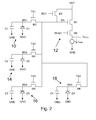
- a section of a memory array having four 2-bit memory locations is shown with two readout arrangements 30, 32 and, referring to Fig. 4B , a further section of the same memory array again having four 2-bit memory locations with two memory arrangements 50, 52.
- Readout arrangement 30 is connected to four memory elements 34B, 36B, 38A and 40A via a common sense node SN1.
- Readout arrangement 32 is shown connected to two memory elements 34A, 36A via a common sense node SN0 but would also be normally connected to two further memory elements in the same manner as readout arrangement 30.
- a transfer gate signal TG ⁇ 1> controls two transfer gate transistors M2 ⁇ 0B> and M2 ⁇ 1 B> and a transfer gate signal TG ⁇ 0> controls two transfer gate transistors M2 ⁇ 0A> and M2 ⁇ 1A>.
- each readout arrangement 30, 32, 50, 52 are alternately connected to a separate VRT line VRT ⁇ 1> and VRT ⁇ 0>.
- Separate VRT lines mean that the layout of the array has to be modified slightly from a standard pixel array layout for use as memory.
- VRT lines are preferable because with a pixel array, a pixel was only required to be individually addressed on readout, which was typically done in parallel a row at a time.
- a row select signal which would activate the read transistor, would be activated along with a transfer gate transistor and the pixel values would be readout.
- the VRT signal in a pixel array would remain "high" during the time that the pixel array was active and therefore was common across the whole pixel array.
- the VRT lines in this context are bit lines and are used to write data to the bit node of the memory element.
- the VRT lines are made common only to a row or column. It would be possible to write data to all memory elements with an array wide common VRT line by selecting the relevant transfer gate transistor and applying the relevant bit signal to the common VRT line.
- the transfer gate signal TX in Fig. 1
- the transfer gate signal TX is common to a row and therefore selects a pixel in each column when activated. In the example of Fig.
- a transfer gate signal such as TG ⁇ 1> selects two memory locations, in this case 36A and 36B, in each column.
- VRT ⁇ 0> and VRT ⁇ 1> are, separately, common across a column, selecting TG ⁇ 1> and applying two data signals, one to VRT ⁇ 0> and the other to VRT ⁇ 1>, writes data to the memory locations 36A and 36B. For a large pixel array this would mean that two memory locations can be written to or read from per column in parallel.
- Fig. 5 shows an example of timings for signals required to write data.
- voltage values described are used as examples of values and other values may be used.
- VRT ⁇ 0> is set to "1 ", which in this case is 2.5V, and RST ⁇ 0> and TG ⁇ 1> are set to high (3.5V in this case), turning on transistors M0 ⁇ 0> and M2 ⁇ 0B>.
- Fig. 5 the timing is shown to write to the 2-bit locations of Fig. 4A .
- the timing diagram of Fig. 5 also refers to RST ⁇ 2> and RST ⁇ 3>, which are shown on Fig. 4B and represent signals for further reset transistors M0 ⁇ 2> and M0 ⁇ 3> of further readout arrangements identical to that of 30 and 32 repeated above that of the memory locations and readout arrangements shown.
- RD ⁇ 0> and RD ⁇ 1> are set low (0V) and corresponding signals RD ⁇ 2> and RD ⁇ 3> of readout arrangements 50 and 52 in Fig. 4B are also set low.
- Each VRT line (VRT ⁇ 1>, VRT ⁇ 0>) is driven by a multiplexer that will drive one of three possible voltages onto the appropriate VRT line, 2.5V, 2.2V or 0V.
- 2.5V is used on the VRT line to write logic high data or when the memory is being read out.
- 2.2V is used on the VRT line when the memory is being read out, during the sense amplifier calibration stage.
- 0V is used on the VRT line to write logic low data to the memory cell. Note, in reality 0V would not be used but a value close to this but slightly higher, i.e. 100mV. However, 0V will still be referred to in the following explanation.
- a first write operation is to store two "0"s at the two bit memory location 34A and 34B.
- VRT ⁇ 0> and VRT ⁇ 1> are set to low (0V in this case) and RST ⁇ 0> and RST ⁇ 1> are set to high (3.5V in this case).
- TG ⁇ 0> which was low meaning that transfer gate transistors M2 ⁇ 0A> and M2 ⁇ 1A> were "off”, is then also set to high (3.5V in this case), turning M2 ⁇ 0A> and M2 ⁇ 1A> "on”, before being set back to low. This stores a "0" at memory location 34A and 34B.
- VRT ⁇ 0> is set to high and VRT ⁇ 1> is set to low with RST ⁇ 0> and RST ⁇ 1> still set high from the previous write operation.
- TG ⁇ 1> which was low meaning that transfer gate transistors M2 ⁇ 0B> and M2 ⁇ 1 B> were "off”, is then also set to high, turning M2 ⁇ 0B> and M2 ⁇ 1B> "on", before being set back to low. This stores a "1" at memory location 36A and a "0" at memory location 36B.
- a third write operation is to store a "1" and a "0" at the two bit memory location 40A and 40B.
- VRT ⁇ 1> is set to high and VRT ⁇ 0> is set to low with RST ⁇ 0> going low, as it is no longer required, RST ⁇ 1> still set high from the previous write operation and RST ⁇ 2> also being set high.
- TG ⁇ 2> is then set to high before being set back to low. This stores a "1" at memory location 40A and a "0" at memory location 40B.
- a fourth write operation is to store two "1"s at the two bit memory location 38A and 38B.
- VRT ⁇ 1> and VRT ⁇ 0> are set to high with RST ⁇ 1> and RST ⁇ 2> still set high from the previous write operation.
- TG ⁇ 3> is then set to high before being set back to low. This stores a "1" at memory locations 38A and 38B.
- signals TG ⁇ 0> to TG ⁇ 3>, RST ⁇ 0> to RST ⁇ 3> and RD ⁇ 0> to RD ⁇ 3> are shown and provide signals to the relevant components as previously described.
- VRT ⁇ 0> and VRT ⁇ 1> are also shown with the same signal being used on all VRT lines.
- VRT lines there is a read sequence comprising of three stages to read data from a memory location. This read sequence is then repeated for subsequent memory locations. It can also be seen that all VRT lines have the same waveforms present on them during the read sequence, where the voltage on the VRT lines, in this example, is either 2.2V or 2.5V.
- 2.2V is first applied to the VRT lines, in this example, because it is the nominal case average voltage found when summing a one and a zero.
- a one is represented by approximately 2.5V on the sense node following read out.
- a zero is represented by approximately 1.9V on the sense node following read out, as the sense node voltage will drop if the bit node is 0V (or is approximately 0V).
- the average value is 2.2V.
- the sense amplifier will be able to detect the data on the bit node accordingly.
- part 1 of the read sequence is required to calibrate the sense amplifier.
- a first RST pulse such as RST ⁇ 0> pulse 60, applies 2.2V to the sense node and then the VRT lines are set to 2.5V for sufficient time to allow the sense amplifier (or readout arrangement) to be correctly calibrated.
- a second RST pulse such as RST ⁇ 0> pulse 62, resets the sense node to 2.5V.
- Part 3 of the read sequence is where the TG (transfer gate) line pulses, such as TG ⁇ 0> pulse 64, and data transfer from the bit node onto the sense node takes place, that is, the data is read out.
Landscapes
- Engineering & Computer Science (AREA)
- Multimedia (AREA)
- Signal Processing (AREA)
- Physics & Mathematics (AREA)
- Power Engineering (AREA)
- Electromagnetism (AREA)
- Condensed Matter Physics & Semiconductors (AREA)
- General Physics & Mathematics (AREA)
- Computer Hardware Design (AREA)
- Microelectronics & Electronic Packaging (AREA)
- Transforming Light Signals Into Electric Signals (AREA)
- Dram (AREA)
Priority Applications (2)
| Application Number | Priority Date | Filing Date | Title |
|---|---|---|---|
| EP08275042A EP2151828A1 (fr) | 2008-08-04 | 2008-08-04 | Circuit de mémoire à accès aléatoire |
| US12/535,261 US8456885B2 (en) | 2008-08-04 | 2009-08-04 | Random access memory circuit |
Applications Claiming Priority (1)
| Application Number | Priority Date | Filing Date | Title |
|---|---|---|---|
| EP08275042A EP2151828A1 (fr) | 2008-08-04 | 2008-08-04 | Circuit de mémoire à accès aléatoire |
Publications (1)
| Publication Number | Publication Date |
|---|---|
| EP2151828A1 true EP2151828A1 (fr) | 2010-02-10 |
Family
ID=40139332
Family Applications (1)
| Application Number | Title | Priority Date | Filing Date |
|---|---|---|---|
| EP08275042A Withdrawn EP2151828A1 (fr) | 2008-08-04 | 2008-08-04 | Circuit de mémoire à accès aléatoire |
Country Status (2)
| Country | Link |
|---|---|
| US (1) | US8456885B2 (fr) |
| EP (1) | EP2151828A1 (fr) |
Families Citing this family (3)
| Publication number | Priority date | Publication date | Assignee | Title |
|---|---|---|---|---|
| KR101139477B1 (ko) * | 2010-06-25 | 2012-04-30 | 에스케이하이닉스 주식회사 | 이미지 센서 |
| JP5959187B2 (ja) * | 2011-12-02 | 2016-08-02 | オリンパス株式会社 | 固体撮像装置、撮像装置、および信号読み出し方法 |
| US10373991B2 (en) * | 2015-08-19 | 2019-08-06 | Semiconductor Energy Laboratory Co., Ltd. | Imaging device, operating method thereof, and electronic device |
Citations (6)
| Publication number | Priority date | Publication date | Assignee | Title |
|---|---|---|---|---|
| US20040262495A1 (en) * | 2003-06-27 | 2004-12-30 | Casio Computer Co., Ltd. | Method for setting individual information of solid-state image sensor, solid-state image sensor, and imaging device |
| EP1628468A2 (fr) * | 2004-08-11 | 2006-02-22 | Sony Corporation | Dispositif de prise d'images à l'état solide et appareil de prise d'images |
| EP1780795A1 (fr) * | 2004-07-20 | 2007-05-02 | Fujitsu Limited | Élément cmos d"imagerie |
| WO2008036289A1 (fr) * | 2006-09-21 | 2008-03-27 | Micron Technology, Inc. | Dispositif de capteur d'image possédant un ou plusieurs pixels factices modifiés qui sont utilisables comme éléments de mémoire non volatile |
| US20080117319A1 (en) * | 2006-11-16 | 2008-05-22 | Micron Technology, Inc. | Imager device with anti-fuse pixels and recessed color filter array |
| WO2008063419A1 (fr) * | 2006-11-16 | 2008-05-29 | Aptina Imaging Corporation | Procédé, appareil et système de fourniture de cellules de mémoire associées à un ensemble de pixels |
Family Cites Families (4)
| Publication number | Priority date | Publication date | Assignee | Title |
|---|---|---|---|---|
| FR2844398A1 (fr) * | 2002-09-11 | 2004-03-12 | St Microelectronics Sa | Photodetecteur d'un capteur d'images |
| US7369167B2 (en) * | 2003-06-02 | 2008-05-06 | Micron Technology, Inc. | Photo diode ID for CMOS imagers |
| JP3976754B2 (ja) * | 2004-07-13 | 2007-09-19 | マイクロン テクノロジー,インコーポレイテッド | 選択読取りによる広ダイナミックレンジ撮像デバイス |
| US7447085B2 (en) * | 2006-08-15 | 2008-11-04 | Micron Technology, Inc. | Multilevel driver |
-
2008
- 2008-08-04 EP EP08275042A patent/EP2151828A1/fr not_active Withdrawn
-
2009
- 2009-08-04 US US12/535,261 patent/US8456885B2/en active Active
Patent Citations (6)
| Publication number | Priority date | Publication date | Assignee | Title |
|---|---|---|---|---|
| US20040262495A1 (en) * | 2003-06-27 | 2004-12-30 | Casio Computer Co., Ltd. | Method for setting individual information of solid-state image sensor, solid-state image sensor, and imaging device |
| EP1780795A1 (fr) * | 2004-07-20 | 2007-05-02 | Fujitsu Limited | Élément cmos d"imagerie |
| EP1628468A2 (fr) * | 2004-08-11 | 2006-02-22 | Sony Corporation | Dispositif de prise d'images à l'état solide et appareil de prise d'images |
| WO2008036289A1 (fr) * | 2006-09-21 | 2008-03-27 | Micron Technology, Inc. | Dispositif de capteur d'image possédant un ou plusieurs pixels factices modifiés qui sont utilisables comme éléments de mémoire non volatile |
| US20080117319A1 (en) * | 2006-11-16 | 2008-05-22 | Micron Technology, Inc. | Imager device with anti-fuse pixels and recessed color filter array |
| WO2008063419A1 (fr) * | 2006-11-16 | 2008-05-29 | Aptina Imaging Corporation | Procédé, appareil et système de fourniture de cellules de mémoire associées à un ensemble de pixels |
Also Published As
| Publication number | Publication date |
|---|---|
| US8456885B2 (en) | 2013-06-04 |
| US20100061139A1 (en) | 2010-03-11 |
Similar Documents
| Publication | Publication Date | Title |
|---|---|---|
| US9860471B2 (en) | Solid-state imaging device | |
| US6927433B2 (en) | Active pixel image sensor with two transistor pixel, in-pixel non-uniformity correction, and bootstrapped reset lines | |
| KR100797506B1 (ko) | 증폭형 고체 촬상 장치 | |
| US8217328B2 (en) | Low noise pixel readout circuit with high conversion gain | |
| US11189651B2 (en) | Image sensor | |
| US9584739B2 (en) | CMOS image sensor with processor controlled integration time | |
| US7567281B2 (en) | Solid state imaging device, method for driving the same, and camera | |
| US20090002538A1 (en) | Solid state imaging apparatus, method for driving the same and camera using the same | |
| US20060197858A1 (en) | Amplifying solid-state imaging device, and method for driving the same | |
| US20110205417A1 (en) | Method and image sensor pixel without address transistor | |
| KR101461624B1 (ko) | 데이터의 고속 리드아웃을 위한 이미지 센서 | |
| US10194106B2 (en) | Image sensor and sensing method thereof | |
| US7602429B2 (en) | Paired differential active pixel sensor | |
| JP2005086595A (ja) | 半導体装置並びに半導体装置を構成する単位構成要素の駆動制御方法および駆動制御装置 | |
| JP6062800B2 (ja) | 撮像装置および撮像表示システム | |
| CN109637453B (zh) | 显示面板及其驱动方法、显示装置 | |
| CN110191295B (zh) | 运用经划分位线的cmos图像传感器箝位方法 | |
| JP2011015158A (ja) | 固体撮像装置 | |
| KR101387895B1 (ko) | 반도체 장치 | |
| US8259199B2 (en) | Pixel array with reduced sensitivity to defects | |
| EP2151828A1 (fr) | Circuit de mémoire à accès aléatoire | |
| US11244976B2 (en) | Photoelectric conversion device, photoelectric conversion system, and signal processing device | |
| US10574923B2 (en) | Image capturing device and driving method thereof | |
| JP2005198239A (ja) | 感度に優れたイメージセンサ及びその駆動方法 | |
| CN101874273A (zh) | 用于cmos成像像素检测器的紧凑且精确的模拟存储器 |
Legal Events
| Date | Code | Title | Description |
|---|---|---|---|
| PUAI | Public reference made under article 153(3) epc to a published international application that has entered the european phase |
Free format text: ORIGINAL CODE: 0009012 |
|
| AK | Designated contracting states |
Kind code of ref document: A1 Designated state(s): AT BE BG CH CY CZ DE DK EE ES FI FR GB GR HR HU IE IS IT LI LT LU LV MC MT NL NO PL PT RO SE SI SK TR |
|
| AX | Request for extension of the european patent |
Extension state: AL BA MK RS |
|
| 17P | Request for examination filed |
Effective date: 20100806 |
|
| 17Q | First examination report despatched |
Effective date: 20100831 |
|
| AKX | Designation fees paid |
Designated state(s): DE FR GB |
|
| STAA | Information on the status of an ep patent application or granted ep patent |
Free format text: STATUS: THE APPLICATION IS DEEMED TO BE WITHDRAWN |
|
| 18D | Application deemed to be withdrawn |
Effective date: 20140301 |