EP2148747B1 - Dünnschichten aus konjugierten polymeren mit anorganischen nanopartikeln und herstellungsverfahren dafür - Google Patents
Dünnschichten aus konjugierten polymeren mit anorganischen nanopartikeln und herstellungsverfahren dafür Download PDFInfo
- Publication number
- EP2148747B1 EP2148747B1 EP08805859.9A EP08805859A EP2148747B1 EP 2148747 B1 EP2148747 B1 EP 2148747B1 EP 08805859 A EP08805859 A EP 08805859A EP 2148747 B1 EP2148747 B1 EP 2148747B1
- Authority
- EP
- European Patent Office
- Prior art keywords
- type
- support
- organic
- process according
- film
- Prior art date
- Legal status (The legal status is an assumption and is not a legal conclusion. Google has not performed a legal analysis and makes no representation as to the accuracy of the status listed.)
- Not-in-force
Links
Images



Classifications
-
- B—PERFORMING OPERATIONS; TRANSPORTING
- B05—SPRAYING OR ATOMISING IN GENERAL; APPLYING FLUENT MATERIALS TO SURFACES, IN GENERAL
- B05D—PROCESSES FOR APPLYING FLUENT MATERIALS TO SURFACES, IN GENERAL
- B05D7/00—Processes, other than flocking, specially adapted for applying liquids or other fluent materials to particular surfaces or for applying particular liquids or other fluent materials
-
- H—ELECTRICITY
- H10—SEMICONDUCTOR DEVICES; ELECTRIC SOLID-STATE DEVICES NOT OTHERWISE PROVIDED FOR
- H10K—ORGANIC ELECTRIC SOLID-STATE DEVICES
- H10K30/00—Organic devices sensitive to infrared radiation, light, electromagnetic radiation of shorter wavelength or corpuscular radiation
- H10K30/10—Organic devices sensitive to infrared radiation, light, electromagnetic radiation of shorter wavelength or corpuscular radiation comprising heterojunctions between organic semiconductors and inorganic semiconductors
-
- H—ELECTRICITY
- H10—SEMICONDUCTOR DEVICES; ELECTRIC SOLID-STATE DEVICES NOT OTHERWISE PROVIDED FOR
- H10K—ORGANIC ELECTRIC SOLID-STATE DEVICES
- H10K30/00—Organic devices sensitive to infrared radiation, light, electromagnetic radiation of shorter wavelength or corpuscular radiation
- H10K30/30—Organic devices sensitive to infrared radiation, light, electromagnetic radiation of shorter wavelength or corpuscular radiation comprising bulk heterojunctions, e.g. interpenetrating networks of donor and acceptor material domains
- H10K30/35—Organic devices sensitive to infrared radiation, light, electromagnetic radiation of shorter wavelength or corpuscular radiation comprising bulk heterojunctions, e.g. interpenetrating networks of donor and acceptor material domains comprising inorganic nanostructures, e.g. CdSe nanoparticles
-
- H—ELECTRICITY
- H10—SEMICONDUCTOR DEVICES; ELECTRIC SOLID-STATE DEVICES NOT OTHERWISE PROVIDED FOR
- H10K—ORGANIC ELECTRIC SOLID-STATE DEVICES
- H10K85/00—Organic materials used in the body or electrodes of devices covered by this subclass
- H10K85/10—Organic polymers or oligomers
- H10K85/111—Organic polymers or oligomers comprising aromatic, heteroaromatic, or aryl chains, e.g. polyaniline, polyphenylene or polyphenylene vinylene
- H10K85/113—Heteroaromatic compounds comprising sulfur or selene, e.g. polythiophene
-
- B—PERFORMING OPERATIONS; TRANSPORTING
- B05—SPRAYING OR ATOMISING IN GENERAL; APPLYING FLUENT MATERIALS TO SURFACES, IN GENERAL
- B05D—PROCESSES FOR APPLYING FLUENT MATERIALS TO SURFACES, IN GENERAL
- B05D1/00—Processes for applying liquids or other fluent materials
- B05D1/18—Processes for applying liquids or other fluent materials performed by dipping
-
- H—ELECTRICITY
- H10—SEMICONDUCTOR DEVICES; ELECTRIC SOLID-STATE DEVICES NOT OTHERWISE PROVIDED FOR
- H10K—ORGANIC ELECTRIC SOLID-STATE DEVICES
- H10K30/00—Organic devices sensitive to infrared radiation, light, electromagnetic radiation of shorter wavelength or corpuscular radiation
- H10K30/50—Photovoltaic [PV] devices
-
- Y—GENERAL TAGGING OF NEW TECHNOLOGICAL DEVELOPMENTS; GENERAL TAGGING OF CROSS-SECTIONAL TECHNOLOGIES SPANNING OVER SEVERAL SECTIONS OF THE IPC; TECHNICAL SUBJECTS COVERED BY FORMER USPC CROSS-REFERENCE ART COLLECTIONS [XRACs] AND DIGESTS
- Y02—TECHNOLOGIES OR APPLICATIONS FOR MITIGATION OR ADAPTATION AGAINST CLIMATE CHANGE
- Y02E—REDUCTION OF GREENHOUSE GAS [GHG] EMISSIONS, RELATED TO ENERGY GENERATION, TRANSMISSION OR DISTRIBUTION
- Y02E10/00—Energy generation through renewable energy sources
- Y02E10/50—Photovoltaic [PV] energy
- Y02E10/549—Organic PV cells
-
- Y—GENERAL TAGGING OF NEW TECHNOLOGICAL DEVELOPMENTS; GENERAL TAGGING OF CROSS-SECTIONAL TECHNOLOGIES SPANNING OVER SEVERAL SECTIONS OF THE IPC; TECHNICAL SUBJECTS COVERED BY FORMER USPC CROSS-REFERENCE ART COLLECTIONS [XRACs] AND DIGESTS
- Y10—TECHNICAL SUBJECTS COVERED BY FORMER USPC
- Y10T—TECHNICAL SUBJECTS COVERED BY FORMER US CLASSIFICATION
- Y10T428/00—Stock material or miscellaneous articles
- Y10T428/24—Structurally defined web or sheet [e.g., overall dimension, etc.]
- Y10T428/24802—Discontinuous or differential coating, impregnation or bond [e.g., artwork, printing, retouched photograph, etc.]
- Y10T428/24917—Discontinuous or differential coating, impregnation or bond [e.g., artwork, printing, retouched photograph, etc.] including metal layer
-
- Y—GENERAL TAGGING OF NEW TECHNOLOGICAL DEVELOPMENTS; GENERAL TAGGING OF CROSS-SECTIONAL TECHNOLOGIES SPANNING OVER SEVERAL SECTIONS OF THE IPC; TECHNICAL SUBJECTS COVERED BY FORMER USPC CROSS-REFERENCE ART COLLECTIONS [XRACs] AND DIGESTS
- Y10—TECHNICAL SUBJECTS COVERED BY FORMER USPC
- Y10T—TECHNICAL SUBJECTS COVERED BY FORMER US CLASSIFICATION
- Y10T428/00—Stock material or miscellaneous articles
- Y10T428/31504—Composite [nonstructural laminate]
Definitions
- fluorescent nanocrystals of semiconductors eg CdSe, CdTe, InP, ZnO
- gold nanoparticles and nanoparticles of iron oxide or iron-platinum alloy eg. CdSe, CdTe, InP, ZnO
- semiconductor nanocrystals are promising materials for photovoltaic light-to-electricity conversion.
- Other emerging applications include light-emitting diodes.
- Metallic nanoparticles eg Au are used in combination with conjugated polymers in nonvolatile molecular memories, in electrocatalysis or as chemical sensors.
- Magnetic nanoparticles are considered as "bits” of information storage in future magnetic recording media or as constituents of new materials with spin-dependent electron transport (“spintronics” domain).
- NCs nanocrystals
- a first approach to film preparation is to in situ grow the NCs / NPs in the conjugated polymer.
- the NCs or NPs are directly grown in the conjugated polymer [ eg Au NPs in poly (hexylthiophene: J. Mater Chem 2004, 14, p 141 ].
- this method ensures good dispersion of the particles in the polymer, it generally does not provide NCs or NPs with low size dispersion. This is a disadvantage major because the physical properties of NCs / NPs strongly depend on their size.
- NCs or NPs conjugated polymers.
- conjugated polymers such as poly (3-hexylthiophene) or poly (p-phenylene-vinylene) [ eg CdSe / PPV solar cells: J. Appl. Phys. 2005, 97, p. 014914 patent EP1485955 ].
- CdSe semiconductor NCs
- conjugated polymers such as poly (3-hexylthiophene) or poly (p-phenylene-vinylene) [ eg CdSe / PPV solar cells: J. Appl. Phys. 2005, 97, p. 014914 patent EP1485955 ].
- This method is widely used to increase the performance of solar cells based on conjugated polymers and in particular for conjugated polymer-based cells and semiconductor nanocrystals ( EP1485955 ).
- the films obtained may have morphological defects that are difficult to treat by annealing because of the existence of covalent bonds within the film.
- the methods of manufacturing thin layers containing NCs or NPs in a conjugated polymer used to date do not allow an easy and economical implementation while ensuring the control of the morphology and the composition of the material obtained.
- the deposition steps are repeated, generally alternatively, until the desired thickness for the film is obtained.
- the deposit can be made on the whole of the support or on a part of it only.
- an organic-inorganic hybrid film corresponds to a film consisting of organic and inorganic species and in particular to a film comprising successive layers of alternating nature. More precisely it will be polymeric films in which there exist layers of inorganic nanoparticles, conceptually this type of film has an alternation between the polymer layers and the inorganic layers.
- the films in question here are generally considered optically thin films, their thickness is between nanoscale and micrometric scales.
- the process is of the "non-covalent" type in that the cohesion of the film and that of the film on the support is not ensured by covalent type interactions.
- the process does not give rise to the development of covalent bonds between the various constituents of the film, ie the polymer and the nanoparticles, nor to the development of covalent bonds between the support and the constituents of the film in contact with its surface.
- Organic groups of types X and Y correspond to chemical groups having an affinity for each other and in particular chemical groups developing hydrogen bonds with each other.
- This type of bond is a form of association between an electronegative atom and a hydrogen atom, itself linked to a relatively electronegative second atom.
- the two electronegative atoms usually, but not necessarily, belong to the first row of the periodic table of elements, these will be N, O and F.
- the atoms with free pairs, such as oxygen, nitrogen or still halogens, or electronic gaps, like boron, can easily be invested in this type of bond.
- X and Y will typically correspond to chemical groups having functions having electronegative atoms, such as carbonyl functions or imines, or hydrogen as described above, as exists in the alcohol or amine functions.
- the skilled person is able to determine the groups that it is likely to employ in the context of the invention.
- the hydrogen bonds are preferably formed in the pairs Jx / Jy and Kx / Ky.
- X and Y have cyclic structures, typically it will be a 5- or 6-membered ring.
- X and Y can thus for example correspond to the diaminopyrimidine / thymine pair.
- X and Y groups identical or derived groups of the bases present in the nucleic chains in order to take advantage of their complementarity.
- the purine bases, adenine and guanine, and pyrimidines, cytosine, thymine and uracil, as well as their derivatives, of course retaining the structure ensuring the formation of hydrogen bonds, can be used in the context of the invention as group X and Y It is of course preferable that adenine be used in a complementary manner to thymine or uracil, to form two hydrogen bonds, and guanine in a manner complementary to cytosine, for form three hydrogen bonds.
- the choice of couples known for their complementarity is recommended, in these conditions the cohesion of the film is better.
- the conjugated organic polymers correspond to polymeric structures of organic nature in which there is a conjugation.
- These polymers are known from the prior art especially for their applications in the field of electronics, among them there may be mentioned aromatic, heterocyclic, linear or polymer polymers alternating heterocycles and double bonds, and in particular poly (aniline) s, poly (alkylthiophene) s, poly ( p -phenylene) s, poly ( p -phenylenevinylene) s, poly (fluorene) s, poly (pyrrole) s, poly (acetylene) s, polyaromatic amines, poly (thienylene-vinylene) and their soluble derivatives which do not form part of the invention.
- conjugated organic polymers having X-type organic groups are generally copolymers derived from a conjugated polymer as defined above, having modified monomeric units which comprise the group X.
- the X group will be present on a side chain so that it does not disturb the conjugation within the polymer, the amount of monomeric unit having a substitution with a group X will generally be between 5 and 50%, and particularly between 5 and 15%.
- a polymer comprising organic groups of type X such as a 3-hexylthiophene polymer having, at a level of 10 to 15%, monomeric units carrying an organic group of type X as a 3-hexylthiophene bonded to a 6-oxy-2,4-diaminopyrimidine at the end of the hexyl chain, as illustrated by figure 1 .
- the X groups employed within the polymer are of a similar nature and advantageously that they are identical.
- the methods of preparation of the polymers are known in organic chemistry, the integration of the X group can be easily achieved by derivatization of a monomeric unit as illustrated by the experimental part or as one can find it in the literature, as such it is useful to refer to Mouffouk et al. CHEM. COMMON. (2004) 2314 .
- a nanoparticle corresponds to an inorganic particle of nanometric size, it may especially be nanocrystals (NC).
- the NPs typically consist of at least one metal and / or at least one semiconductor compound comprising at least one metal.
- the metals may be chosen in particular from transition metals, rare earths, metals of groups IIIA, IVA and VA of the periodic table of the elements, their alloys, their oxides and mixtures of these metals and alloys. More particularly, the invention applies to gold, platinum, silver, copper, titanium oxide, iron oxide, iron-platinum, iron-palladium and cobalt-metal alloys. platinum.
- semiconductors it may for example be compounds of formula AB with A an element whose oxidation state is + II and B an element whose oxidation state is -II, typically A is selected from Mg, Ca, Sr, Ba, Zn, Cd, Hg, Sn, Pb and mixtures thereof, and B is selected from O, S, Se, Te and mixtures thereof.
- the semiconductors that may be mentioned are the semiconductors of formula CD with C being an element whose oxidation state is + III and D being an element whose oxidation state is -III, typically C is chosen from Al, Ga, In and mixtures of these elements, and D is chosen from N, P, As, Sb, Bi and mixtures of these elements.
- the particles used in the photovoltaic field or in the electronic memories are particularly relevant to the invention, it is particularly particles of CdSe, CdTe, ZnO, PbSe, PbS, InP, InN, CulnS 2, CulnSe 2, Cu (In, Ga) Se 2 , GaAs, InGaAs, Si, Ge, Au, Ag and Pt.
- CdSe NPs, InP and CulnSe 2 perhaps also Cu (In, Ga) Se 2 and CulnS 2 and in the domain of Au, Ag and Pt electronic memories.
- nanoparticles comprising Y-type organic groups.
- Such nanoparticles are organic-inorganic hybrid entities. It is in particular a nanoparticle, as presented above, to which is bonded one or more organic ligand comprising a group of type Y.
- a nanoparticle of this type typically has an inorganic core, consisting of at least a metal and / or at least one semiconductor compound comprising at least one metal, to which is bonded at least one ligand comprising an organic group of type Y which constitutes a coating, where crown, of organic nature.
- the ligands that may be used in the context of the invention are in particular ligands of formula (III): BG - (SG) p - Y
- BG will be chosen depending on the type of nanoparticle that is employed in the process.
- BG can bind covalently, by complexation, chelation, or by electrostatic interaction on the surface of nanoparticles.
- those skilled in the art may in particular refer to the prior art and particularly to the Colloids and Colloid Assemblies, Frank Caruso (Ed.), 1. Ed. Dec. 2003, Wiley-VCH, Weinheim .
- BG can especially be a thiol, a dithiol, a carbodithioate, dithiocarbamate, xanthate, when the particle corresponds to a metal such as gold, silver, copper, platinum, palladium or when it corresponds to a AB type semiconductor such as CdSe, CdTe, ZnO, PbSe, PbS, CulnS 2, CulnSe 2 or Cu (In, Ga) Se 2.
- oxide nanoparticles such as titanium, zirconium, aluminum or iron oxide
- BG may especially correspond to a carboxylic acid, dicarboxylic acid, phosphonic acid, diphosphonic acid, sulfonic acid or hydroxamic acid.
- the acids may be in deprotonated form, as has been explained in the prior art and in particular in the patent application WO2004097871 .
- a spacer group SG generally corresponds to a group which generally does not develop any interaction other than of steric nature or of affinity of hydrophilic or hydrophobic type with the inroganic heart. the nanoparticle, the polymer and the substrate, and that does not react with them.
- the spacer may be a carbon chain containing no heteroatom, it may for example be a chain of aliphatic nature, eg alkyl chain, preferably of 1-12 carbon atoms, a chain aromatic, or a heterocyclic chain.
- CdSe NPs functionalized with 1- (6-mercaptohexylthymine).
- Another example corresponds to gold NPs or iron oxide NPs, functionalized according to the processes described in the articles. Nature 2000, 404, p. 746 and Chem. Mast. 2004, 16, p. 3252 with ligands containing a thymine group.
- carbodithioate, dithiocarbamate or xanthate type molecules containing a thymine function for the functionalization of CdSe nanocrystals as described in the patent application. EP1548431 .
- the support may be of a variable nature, considering that the invention makes it possible to provide, in particular, devices in the field of electronics, it is desirable to apply the method to supports consisting of materials used in this field.
- the invention corresponds to a method of coating a support, only the nature of the surface of the support is likely to interact directly with the constituents of the film covering it.
- it may especially be supports having a surface of metal, metal alloys, or semiconductor.
- it is recommended to choose supports on the surface of which there are oxides, in particular to allow the formation of hydrogen bonds between the surface of the support and the polymer or the nanoparticles in its vicinity.
- the X-type organic groups correspond to groups having the majority of the covalent bonds with the hydrogens capable of being engaged in hydrogen bonds with Y, so that part of the X groups present in the molecules of polymers closest to the surface can also develop hydrogen bonds with the support to significantly increase the cohesion of the film with the support.
- the support may for example be selected from glass, mica, silicon, generally having an oxide layer, or indium tin oxide (ITO).
- Steps (a) and (b) are typically performed successively, as previously indicated, it is further preferable that the first step is step (a).
- steps (a) and (b) are carried out using liquid solutions comprising the polymer or the nanoparticles. These solutions are prepared with a solvent adapted to the compound to be solubilized or dispersed. Those skilled in the art are able to determine the solvent that can be used according to what it wishes to solubilize or disperse, it is recommended to test different solvents according to their polarity to determine the solvent ensuring solubilization or sufficient dispersion .
- a solvent in which it is possible to solubilize the polymer having X groups at a concentration of at least 0.1 g / L.
- the same solvent or a solvent of similar polarity as that used for the conjugated polymer having no group X and especially when their molecular mass is close, ie the difference is at most equal to 10%.
- the appropriate solvents are rather aprotic and apolar.
- the regioregular poly (hexylthiophene), with typically M n close to 12800 g / mol, comprising diaminopyrimidine functions can be solubilized in chloroform.
- a solvent that allows the nanoparticles to disperse at a concentration of at least 0.1 g / L is recommended to choose a solvent that allows the nanoparticles to disperse at a concentration of at least 0.1 g / L.
- the suitable solvents are rather aprotic and polar, it may for example be N, N-dimethylformamide (DMF).
- DMF N, N-dimethylformamide
- methanol typically 10% by volume.
- CdSe NPs functionalized with 1- (6-mercaptohexylthymine) can be dispersed in a N, N-dimethylformamide / methanol (10/1 by volume) mixture.
- the solvents used in the synthesis of the nanoparticles that the user wishes to use are often suitable for carrying out dispersion, it is useful to refer to the associated procedures.
- nanoparticles / nanocrystals it is often advantageous to apply ultrasonic treatment to the solution to promote dispersion.
- Steps (a) and (b) may in particular be carried out by spraying the solutions on the support.
- the steps (a) and (b) are carried out by dipping the support in the corresponding solution, this type of procedure, known as layer-by-layer (LBL) deposition, is particularly suitable because it allows a control on the amount of compound that will be deposited on the support.
- LBL layer-by-layer
- the support is immersed in the solution for a variable time which may be between a few minutes (for example 5 minutes using a concentration of 0.25 g / l), and a few tens of minutes (for example 45 minutes using a concentration of 4 g / L), depending on the amount of compound that the user wishes to deposit on the support and therefore according to the thickness that it wishes to give to the layer.
- each of the layers can easily be modulated by varying the soaking time, and the concentration of the species to be deposited in the solvent.
- An important latitude is given to the user with this technique according to the type of application that he envisages, the person skilled in the art could in this respect refer to the literature and for example to Adv. Mater. 2004, 16, p. 823 which illustrates, for the poly (p-phenylene vinylene), the ratio thickness of the thin polymer layer / soaking time.
- m and n will be such that the multilayer film has a total thickness of between a few nanometers or a few tens of nanometers, m and n are equal to 1 in this case, and up to a few hundred nanometers with in general values of m and n greater than 10. Thicknesses around 100 nm are typically attained for values of m and n between 6 and 10. Of course measurements can be made to control the thickness of the film using a profilometer, or the X-ray scattering method at small angles. Usefully the skilled person can refer to the example described below.
- the elements of the film may in particular be as defined above.
- the invention also relates to a support, as defined above, covered with a film as defined above.
- such a device will be a photovoltaic cell and particularly a volume heterojunction photovoltaic cell comprising at least two electrodes electrically connected to each other by the film according to the invention.
- the electrodes can be independently conductive or semiconducting.
- a conductive electrode comprises a metal surface of metals such as gold, calcium, aluminum, silver, magnesium, chromium, lithium, or metal alloys. It may also comprise a stack of metal layers and / or conductive oxide such as In 2 O 3 / SnO 2 .
- a semiconductor electrode comprises silicon. AsGa, Ge, SiC
- the semiconductor electrode may optionally be deposited on an insulating material such as silica, alumina or glass
- at least one of the electrodes is transparent.
- Such a cell can be made from a glass support comprising an ITO layer previously etched with aqua regia to remove a portion, Cr-Au pads are then deposited on the ITO and on the glass.
- a layer of PEDOT-PSS poly (3,4-ethylenedioxythiophene) -poly (styrene sulfonate) may optionally be deposited by spin-coating.
- the studs on the glass are clear.
- the active layer which corresponds to the film previously exposed, is then deposited by dipping layer by layer. Once the active layer deposited the pads are released and the back side is cleaned.
- the supports are then placed in a frame in which the LiF-Al layer, the thickness of which is generally between 1.3 and 70, is deposited.
- the invention relates to the use of films, supports covered with films and devices as described above, in the field of electronics and in particular photovoltaic and particularly in a photovoltaic cell.
- the invention discloses a novel method of making thin films containing inorganic NCs or NPs in a conjugated polymer. It is based on the use of non-covalent interactions between NCs or NPs and the conjugated polymer. According to the provisions set out, a thin film composed of NCs and a conjugated polymer can be produced simply by repeatedly dipping a support in a solution containing the polymer and then in a solution containing the NCs.
- the solvents used in the context of the invention are generally of organic type and are therefore compatible with the conjugated polymers and NCs / NPs.
- the total thickness of the film is controlled at the nanoscale by the number of layers deposited as well as by parameters such as the concentration of solutions and soaking time of the support.
- the advantage of the technique is also based on the fact that the deposition of a bonding layer on the substrate is not necessary, the functionalized polymer ensuring the double bonding of the polymer on the surface of the support and NCs on the polymer .
- this method is very economical since only the deposited material is consumed.
- the resulting film does not present aggregates due to a natural demixing of the two components NCs and conjugated polymer through the existence of hydrogen bonds.
- the presence of intermediate bonds that is to say weaker than covalent and stronger bonds than Van der Waals bonds, also gives more flexibility in terms of self-organization of the organic / inorganic material. and make it possible to modify its morphology by a treatment of thermal annealing type after deposition.
- the figure 1 corresponds to the representation of two monomeric units of a 3-hexylthiophene polymer having X-type organic groups, one of the monomeric units is a 3-hexylthiophene bonded to a 6-oxy-2,4-diaminopyrimidine end of the hexyl chain.
- the figure 2 corresponds to the schematic representation of the establishment of a triple hydrogen bond between the group DAP (diaminopyrimidine) present at the end of the alkyl chain of the polymer and the Thy (thymine) group introduced by exchange reaction on the surface of NCs of CdSe.
- DAP diaminopyrimidine
- Thy thymine
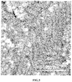
- the figure 3 corresponds to a scanning electron microscopy image of a deposit of a single P3HT-DAP / CdSe-Thy bilayer on an ITO substrate.
- the figure 4 represents the UV-vis absorption spectrum recorded during layer-by-layer deposition of the hybrid for each P3HT-DAP / CdSe-Thy bilayer, the absorbance (in arbitrary unit) at a wavelength 500 nm being characteristic of the polymer and the absorbance at 622 nm characteristic of the NCs, in inset appears the evolution as a function of the number of bilayers (number of bilayers) polymer / NP.
- the figure 5 corresponds to the schematic representation of a photovoltaic cell.
- 3- (6-Bromohexyl) thiophene was first synthesized by reaction between 3-bromothiophene and 1,6-dibromohexane according to the protocol described by Zhai et al [Macromolecules, 2003, 36, p. 61 ].
- the experimental setup is first evacuated and then under an inert atmosphere (Argon).
- 3-bromothiophene (5.38 g, 33 mmol) and 30 ml of anhydrous hexane, the medium was cooled to -40 ° C using a bath of acetone / liquid nitrogen and stirred for 15 minutes.
- the initial ratio of the monomers introduced is 1 molar equivalent of 3- (6-bromohexylthiopene) per 3 molar equivalents of 3- (hexylthiophene).
- the proportion of 3- (6-bromohexyl) thiophene units integrated into the copolymer chains is 1 to 5 as determined by the integration of the proton NMR characteristic peaks and confirmed by elemental analysis.
- the polymer obtained was dried under reduced pressure and the powder obtained finely ground before being introduced into a cellulose cartridge placed on a Soxhlet extractor.
- the hot extraction of the polymer was then carried out using a sequence of solvents conventionally used for the polyalkylthiophenes, in the order: acetone, hexane, dichloromethane, tetrahydrofuran and chloroform.
- the extraction of the oligomers was done by acetone and hexane, the longest chains extracted with THF and chloroform, dichloromethane allowed to recover the chains of intermediate size. This sequence is preceded by a hot extraction with methanol to remove all traces of catalyst and unreacted monomers.
- NCs that were obtained have sizes between 3 and 6 nm, their diameter was determined by transmission electron microscopy (TEM).
- the nanocrystals functionalized with MHT lose their solubility in chloroform, but are soluble in solvents such as dimethylsulfoxide and N, N-dimethylformamide.
- the exchange rate with MHT determined by 1 H NMR spectroscopy and thermogravimetry, depends on the reaction conditions.
- the rate can be increased by performing the exchange in a microwave oven.
- a microwave oven which was given a temperature of 45 ° C for a power of 60W.
- the rise in temperature was programmed over a period of 15 minutes, then the medium placed one hour at 45 ° C and to end a descent at room temperature in 20 min.
- the nanocrystals purified in the same manner as for the exchange reaction by conventional route. This time the exchange rate has been estimated at 70%.
- the synthesis protocol that has been used follows the methods described in Chem. Common. 1994, p. 801 & J. Phys. Chem. 2003, 107, p. 7406 .
- the NPs that were obtained have sizes between 2.5 and 6 nm, determined by TEM (transmission electron microscopy).
- NPs functionalized with MHT are soluble in solvents such as dimethylsulfoxide and N, N-dimethylformamide.
- the degree of exchange with the MHT depends on the reaction conditions and is determined by 1 H NMR spectroscopy. For an exchange reaction carried out at 45 ° C. in chloroform for 3 h, the exchange rate which has been obtained is about 80%.
- a solution of the polymer P3HT-DAP in chloroform (1g / L) and a dispersion of the CdSe-Thy nanocrystals in a mixture N, N-dimethylformamide: methanol (10: 1, about 0.2 g / L) were introduced into two beakers.
- ITO indium tin oxide
- the first layer was made by dipping the support in the polymer solution for 2 min and then rinsing with chloroform and drying under argon flow. The support was then immersed in the NCs solution of CdSe for 5 min and then rinsed with chloroform and dried under an argon stream.
- figure 2 is schematically represented the interaction between a nanocrystal and a polymer molecule.
- the support after deposition of a polymer layer and a layer of NCs, was observed by electron microscopy to check the very homogeneous dispersion of the NPs on the support, the image obtained is presented to the figure 3 , over which the irregular structure that corresponds to the rough surface of the ITO can be distinguished in the background, the CdSe nanocrystals appearing as small white grains in the foreground.
- the dipping operation alternately in these two solutions was repeated until 25 layers of each of the species were obtained.
- the growth of the film was followed by UV-vis absorption spectroscopy as shown in FIG. figure 4 .
- the protocol is the same as that described in VII using a dispersion of Au-Thy NPs instead of NCs CdSe-Thy.
- a layer of LiF (1.3 nm) and then of aluminum (70 nm) were deposited by thermal evaporation under vacuum through a mask allowing the definition of the active surface of the cell. (2.8 cm 2 ).
- the device prepared corresponds to that represented in figure 5 .
- the solar cell thus produced was tested under white light AM 1.5 with an illumination power of 100 mW / cm 2 .
Landscapes
- Engineering & Computer Science (AREA)
- Chemical & Material Sciences (AREA)
- Inorganic Chemistry (AREA)
- Electromagnetism (AREA)
- Physics & Mathematics (AREA)
- Nanotechnology (AREA)
- Life Sciences & Earth Sciences (AREA)
- Crystallography & Structural Chemistry (AREA)
- Wood Science & Technology (AREA)
- Materials Engineering (AREA)
- Photovoltaic Devices (AREA)
- Manufacture Of Macromolecular Shaped Articles (AREA)
- Laminated Bodies (AREA)
- Application Of Or Painting With Fluid Materials (AREA)
Claims (16)
- Verfahren zur nicht-kovalenten Beschichtung eines Trägers mit einem organisch-anorganischen Hybridfilm, umfassend die Schritte:- Abscheiden eines konjugierten organischen Polymers, das organische Reste vom Typ X aufweist, auf dem Träger;- Abscheiden von Nanopartikeln, die einen oder mehrere organische Reste vom Typ Y aufweisen, auf dem Träger;wobei die Reste vom Typ X und Y dazu in der Lage sind, Bindungen vom Wasserstofftyp untereinander auszubilden,
wobei das konjugierte organische Polymer, das organische Reste vom Typ X aufweist, mit der Diaminopyrimidin-Funktion funktionalisiertes Poly(3-hexylthiophen) ist. - Verfahren nach Anspruch 1, dadurch gekennzeichnet, dass die Abscheidungsschritte alternierend wiederholt werden.
- Verfahren nach den Ansprüchen 1 und 2, wobei X und Y in deren Innerem für X die Kohlenstoff-enthaltende Struktur der Formel (I):

 - Wasserstoffbindungen in der Lage sind, sich in mindestens zwei der Paare Jx/Jy, Kx/Ky, Lx/Ly zu bilden;- für das Paar Jx/Jy, eines der J ein N oder O bedeutet, das kovalent an einen Wasserstoff gebunden ist, und das andere ein N oder ein O bedeutet, das eine Π-Bindung aufweist;- für das Paar Kx/Ky, eines der K ein Stickstoffatom bedeutet, das kovalent an einen Wasserstoff gebunden ist, und das andere ein N bedeutet, das eine Π-Bindung aufweist;- für das Paar Lx/Ly, die L unabhängig Wasserstoffatome, Kohlenstoffatome, ein N oder ein O, die kovalent an einen Wasserstoff gebunden sind, ein N oder ein O, die eine Π-Bindung aufweisen, bedeuten.
 - Verfahren nach Anspruch 3, wobei X und Y dem Diaminopyrimidin/Thymin-Paar entsprechen.
- Verfahren nach Anspruch 1, wobei die Menge an modifizierten Monomereinheiten, die den Rest X aufweisen, zwischen 5 und 50% liegt.
- Verfahren nach einem der vorhergehenden Ansprüche, dadurch gekennzeichnet, dass die Nanopartikel einen anorganischen Kern aufweisen, der aus mindestens einem Metall und/oder mindestens einer Halbleiterverbindung, die mindestens ein Metall umfasst, gebildet ist, an den mindestens ein Ligand organischer Natur gebunden ist, der einen organischen Rest vom Typ Y aufweist.
- Verfahren nach Anspruch 6, dadurch gekennzeichnet, dass das Metall und/oder mindestens eine Halbleiterverbindung, die mindestens ein Metall umfasst, ausgewählt ist aus CdSe, CdTe, ZnO, PbSe, PbS, InP, InN, CuInS2, CuInSe2, Cu(In,Ga)Se2, GaAs, InGaAs, Si, Ge, Au, Ag und Pt.
- Verfahren nach den Ansprüchen 6 und 7, dadurch gekennzeichnet, dass der Ligand die Formel (III) aufweist:
BG - (SG)p - Y
wobei:- BG eine Bindungsgruppe darstellt, die dazu in der Lage ist, an Nanopartikel zu binden;- SG eine Spacergruppe darstellt;- p gleich 0 oder 1 ist. - Verfahren nach Anspruch 8, dadurch gekennzeichnet, dass BG ein Thiol, ein Dithiol, ein Carbodithioat, ein Dithiocarbamat, ein Xanthat, eine Carbonsäure, eine Dicarbonsäure, eine Phosphonsäure, eine Diphosphonsäure, eine Sulfonsäure oder eine Hydroxamsäure ist.
- Verfahren nach den Ansprüchen 8 und 9, dadurch gekennzeichnet, dass der Spacer aliphatischer Natur ist.
- Verfahren nach einem der vorhergehenden Ansprüche, dadurch gekennzeichnet, dass der Träger ausgewählt ist aus Glas, Glimmer, Silicium, das eine Oxidschicht aufweist, und Indiumzinnoxid (ITO).
- Verfahren nach einem der vorhergehenden Ansprüche, dadurch gekennzeichnet, dass die Abscheidungsschritte durch Tränken des Trägers in Lösungen eines konjugierten organischen Polymers, das organische Reste vom Typ X aufweist und eines oder mehrerer organischer Reste vom Typ Y durchgeführt werden.
- Mehrschichtiger organisch-anorganischer Hybridfilm, umfassend:- m Schichten konjugiertes organisches Polymer, das organische Reste vom Typ X aufweist;- n Schichten Nanopartikel, die einen oder mehrere organische Reste vom Typ Y aufweisen;wobei die Reste vom Typ X und Y dazu in der Lage sind, Bindungen vom Wasserstofftyp untereinander auszubilden
wobei das konjugierte organische Polymer, das organische Reste vom Typ X aufweist, mit der Diaminopyrimidin-Funktion funktionalisiertes Poly(3-hexylthiophen) ist. - Träger, beschichtet mit einem mehrschichtigen organisch-anorganischen Hybridfilm nach Anspruch 13.
- Elektronische Vorrichtung, dadurch gekennzeichnet, dass sie umfasst:- einen teilweise mit einem Film nach den Ansprüchen 13 und 14 beschichteten Träger;- eine metallische Schicht auf zumindest einem Teil des Films;- elektrische Kontakte, angeordnet zwischen einem nicht mit Film bedeckten Teil des Trägers, welcher die Anode darstellt, und der metallischen Schicht, welche die Kathode darstellt.
- Verwendung eines mehrschichtigen organisch-anorganischen Hybridfilms nach Anspruch 13 oder eines mit einem Film beschichteten Trägers nach Anspruch 14 in einer Fotovoltaikzelle.
Applications Claiming Priority (2)
| Application Number | Priority Date | Filing Date | Title |
|---|---|---|---|
| FR0755289A FR2916660B1 (fr) | 2007-05-28 | 2007-05-28 | Couches minces de polymeres conjugues contenant des nanoparticules inorganiques et leur procede de fabrication |
| PCT/FR2008/050915 WO2008152295A2 (fr) | 2007-05-28 | 2008-05-27 | Couches minces de polymères conjugués contenant des nanoparticules inorganiques et leur procédé de fabrication |
Publications (2)
| Publication Number | Publication Date |
|---|---|
| EP2148747A2 EP2148747A2 (de) | 2010-02-03 |
| EP2148747B1 true EP2148747B1 (de) | 2018-11-28 |
Family
ID=39048778
Family Applications (1)
| Application Number | Title | Priority Date | Filing Date |
|---|---|---|---|
| EP08805859.9A Not-in-force EP2148747B1 (de) | 2007-05-28 | 2008-05-27 | Dünnschichten aus konjugierten polymeren mit anorganischen nanopartikeln und herstellungsverfahren dafür |
Country Status (5)
| Country | Link |
|---|---|
| US (1) | US8440258B2 (de) |
| EP (1) | EP2148747B1 (de) |
| JP (1) | JP5100830B2 (de) |
| FR (1) | FR2916660B1 (de) |
| WO (1) | WO2008152295A2 (de) |
Families Citing this family (10)
| Publication number | Priority date | Publication date | Assignee | Title |
|---|---|---|---|---|
| US20110284830A1 (en) * | 2009-01-30 | 2011-11-24 | Zhang-Lin Zhou | Polymer and polymer-nanoparticle compositions |
| GB0907445D0 (en) * | 2009-04-30 | 2009-06-10 | Cambridge Entpr Ltd | Photoresponsive devices |
| WO2011052567A1 (ja) * | 2009-10-30 | 2011-05-05 | 住友化学株式会社 | 有機光電変換素子 |
| PL217816B1 (pl) * | 2010-05-14 | 2014-08-29 | Inst Chemii Fizycznej Polskiej Akademii Nauk | Sposób pokrywania powierzchni materiału nanocząstkami |
| US8946062B2 (en) | 2012-11-21 | 2015-02-03 | Guardian Industries Corp. | Polycrystalline silicon thick films for photovoltaic devices or the like, and methods of making same |
| US11532789B2 (en) | 2018-05-29 | 2022-12-20 | Samsung Electronics Co., Ltd. | Organic thin film including semiconducting polymer and elastomer configured to be dynamic intermolecular bonded with a metal-coordination bond and organic sensor and electronic device including the same |
| FR3098821B1 (fr) * | 2019-07-19 | 2023-05-26 | Isorg | Encre pour une couche d’injection d’électrons |
| US11075348B2 (en) | 2019-08-07 | 2021-07-27 | Samsung Electronics Co., Ltd. | Thin film transistor and thin film transistor array and electronic device |
| JP7589454B2 (ja) * | 2020-06-17 | 2024-11-26 | artience株式会社 | 光電変換素子及び光電変換層形成用組成物 |
| CN114583013A (zh) * | 2022-03-10 | 2022-06-03 | 常州时创能源股份有限公司 | 一种bsg去除方法 |
Citations (3)
| Publication number | Priority date | Publication date | Assignee | Title |
|---|---|---|---|---|
| US20020045045A1 (en) * | 2000-10-13 | 2002-04-18 | Adams Edward William | Surface-modified semiconductive and metallic nanoparticles having enhanced dispersibility in aqueous media |
| US20020155442A1 (en) * | 1996-07-29 | 2002-10-24 | Mirkin Chad A. | Nanoparticles having oligonucleotides attached thereto and uses therefor |
| US20030226498A1 (en) * | 2002-03-19 | 2003-12-11 | Alivisatos A. Paul | Semiconductor-nanocrystal/conjugated polymer thin films |
Family Cites Families (4)
| Publication number | Priority date | Publication date | Assignee | Title |
|---|---|---|---|---|
| US20030077625A1 (en) * | 1997-05-27 | 2003-04-24 | Hutchison James E. | Particles by facile ligand exchange reactions |
| WO2003081683A1 (en) | 2002-03-19 | 2003-10-02 | The Regents Of The University Of California | Semiconductor-nanocrystal/conjugated polymer thin films |
| EP1473745A1 (de) | 2003-04-30 | 2004-11-03 | Ecole Polytechnique Federale De Lausanne (Epfl) | Farbstoffsensibilisierte Solarzelle |
| FR2862955B1 (fr) * | 2003-12-02 | 2006-03-10 | Commissariat Energie Atomique | Nanocristaux inorganiques a couche de revetement organique, leur procede de preparation, et materiaux constitues par ceux-ci. |
-
2007
- 2007-05-28 FR FR0755289A patent/FR2916660B1/fr not_active Expired - Fee Related
-
2008
- 2008-05-27 EP EP08805859.9A patent/EP2148747B1/de not_active Not-in-force
- 2008-05-27 US US12/451,570 patent/US8440258B2/en not_active Expired - Fee Related
- 2008-05-27 WO PCT/FR2008/050915 patent/WO2008152295A2/fr not_active Ceased
- 2008-05-27 JP JP2010509872A patent/JP5100830B2/ja not_active Expired - Fee Related
Patent Citations (3)
| Publication number | Priority date | Publication date | Assignee | Title |
|---|---|---|---|---|
| US20020155442A1 (en) * | 1996-07-29 | 2002-10-24 | Mirkin Chad A. | Nanoparticles having oligonucleotides attached thereto and uses therefor |
| US20020045045A1 (en) * | 2000-10-13 | 2002-04-18 | Adams Edward William | Surface-modified semiconductive and metallic nanoparticles having enhanced dispersibility in aqueous media |
| US20030226498A1 (en) * | 2002-03-19 | 2003-12-11 | Alivisatos A. Paul | Semiconductor-nanocrystal/conjugated polymer thin films |
Also Published As
| Publication number | Publication date |
|---|---|
| US20100183855A1 (en) | 2010-07-22 |
| US8440258B2 (en) | 2013-05-14 |
| FR2916660B1 (fr) | 2010-10-15 |
| WO2008152295A3 (fr) | 2009-02-19 |
| JP5100830B2 (ja) | 2012-12-19 |
| WO2008152295A2 (fr) | 2008-12-18 |
| FR2916660A1 (fr) | 2008-12-05 |
| JP2010527783A (ja) | 2010-08-19 |
| EP2148747A2 (de) | 2010-02-03 |
Similar Documents
| Publication | Publication Date | Title |
|---|---|---|
| EP2148747A2 (de) | Dünnschichten aus konjugierten polymeren mit anorganischen nanopartikeln und herstellungsverfahren dafür | |
| Knapton et al. | Synthesis and properties of metallo-supramolecular poly (p-phenylene ethynylene) s | |
| Fulghum et al. | Conjugated poly (phenylacetylene) films cross-linked with electropolymerized polycarbazole precursors | |
| Zhai et al. | A simple method to generate side-chain derivatives of regioregular polythiophene via the GRIM metathesis and post-polymerization functionalization | |
| Locklin et al. | Conjugated oligothiophene-dendron-capped CdSe nanoparticles: Synthesis and energy transfer | |
| Fogg et al. | Fabrication of quantum dot-polymer composites: Semiconductor nanoclusters in dual-function polymer matrices with electron-transporting and cluster-passivating properties | |
| Petrella et al. | Colloidal TiO2 nanocrystals/MEH-PPV nanocomposites: photo (electro) chemical study | |
| Kim et al. | Precise control of quantum dot location within the P3HT-b-P2VP/QD nanowires formed by crystallization-driven 1D growth of hybrid dimeric seeds | |
| Fulghum et al. | Grafting hole-transport precursor polymer brushes on ITO electrodes: surface-initiated polymerization and conjugated polymer network formation of PVK | |
| JP2007527605A (ja) | 半導体ポリマーブラシを組み込んだ有機電子素子 | |
| KR20200022122A (ko) | 계면활성제로 개량된 풀러렌 유도체를 전자전달층으로 이용한 효율과 대기 안정성이 우수한 역구조 페로브스카이트 태양전지 제조 방법 | |
| Firat et al. | Efficiently two-stage synthesis and characterization of CuSe/Polypyrrole composite thin films | |
| Han et al. | Natural and Nature‐Inspired Biomaterial Additives for Metal Halide Perovskite Optoelectronics | |
| EP2734310A1 (de) | Verfahren zur funktionalisierung von metallnanodrähten und zur herstellung von elektroden | |
| Vijayakumar et al. | Gold nanoparticle assisted self-assembly and enhancement of charge carrier mobilities of a conjugated polymer | |
| Zhang et al. | Photoelectron spectroscopy reveals the impact of solvent additives on poly (3, 4-ethylenedioxythiophene): poly (styrenesulfonate) thin film formation | |
| US7947202B2 (en) | Polymer-nanoparticle compositions and methods of making and using same | |
| Böhm et al. | The influence of nanocrystal aggregates on photovoltaic performance in nanocrystal–polymer bulk heterojunction solar cells | |
| Zotti et al. | Gold nanoparticle linking to polypyrrole and polythiophene: Monolayers and multilayers | |
| Jiang et al. | Surface-initiated ring-opening metathesis polymerization (SI-ROMP): synthesis and electropolymerization of terthiophene-functionalized olefin peripheral dendrons | |
| Antoniadou et al. | Study of hybrid solar cells made of multilayer nanocrystalline titania and poly (3-octylthiophene) or poly-(3-(2-methylhex-2-yl)-oxy-carbonyldithiophene) | |
| WO2022153087A1 (fr) | Fabrication d'une cellule solaire ferrophotovoltaique à très haut rendement utilisant des nanoparticules inorganiques de pérovskite ferroélectrique dans une matrice de biopolymère (ferro-opv) | |
| Mazzio et al. | End-functionalized semiconducting polymers as reagents in the synthesis of hybrid II–VI nanoparticles | |
| Pokrop et al. | Electronic, electrochemical, and spectroelectrochemical properties of hybrid materials consisting of carboxylic acid derivatives of oligothiophene and CdSe semiconductor nanocrystals | |
| EP2917947A1 (de) | Neuartiges verfahren zur herstellung organischer elektronischer vorrichtungen |
Legal Events
| Date | Code | Title | Description |
|---|---|---|---|
| PUAI | Public reference made under article 153(3) epc to a published international application that has entered the european phase |
Free format text: ORIGINAL CODE: 0009012 |
|
| 17P | Request for examination filed |
Effective date: 20091113 |
|
| AK | Designated contracting states |
Kind code of ref document: A2 Designated state(s): AT BE BG CH CY CZ DE DK EE ES FI FR GB GR HR HU IE IS IT LI LT LU LV MC MT NL NO PL PT RO SE SI SK TR |
|
| AX | Request for extension of the european patent |
Extension state: AL BA MK RS |
|
| RAP1 | Party data changed (applicant data changed or rights of an application transferred) |
Owner name: COMMISSARIAT A L'ENERGIE ATOMIQUE ET AUX ENERGIES |
|
| DAX | Request for extension of the european patent (deleted) | ||
| STAA | Information on the status of an ep patent application or granted ep patent |
Free format text: STATUS: EXAMINATION IS IN PROGRESS |
|
| 17Q | First examination report despatched |
Effective date: 20170406 |
|
| RAP1 | Party data changed (applicant data changed or rights of an application transferred) |
Owner name: CENTRE NATIONAL DE LA RECHERCHE SCIENTIFIQUE Owner name: COMMISSARIAT A L'ENERGIE ATOMIQUE ET AUX ENERGIES |
|
| GRAP | Despatch of communication of intention to grant a patent |
Free format text: ORIGINAL CODE: EPIDOSNIGR1 |
|
| STAA | Information on the status of an ep patent application or granted ep patent |
Free format text: STATUS: GRANT OF PATENT IS INTENDED |
|
| RIC1 | Information provided on ipc code assigned before grant |
Ipc: B05D 1/18 20060101ALN20180622BHEP Ipc: B05D 7/00 20060101AFI20180622BHEP Ipc: H01L 51/00 20060101ALI20180622BHEP Ipc: H01L 51/42 20060101ALI20180622BHEP |
|
| RIC1 | Information provided on ipc code assigned before grant |
Ipc: H01L 51/00 20060101ALI20180705BHEP Ipc: B05D 7/00 20060101AFI20180705BHEP Ipc: B05D 1/18 20060101ALN20180705BHEP Ipc: H01L 51/42 20060101ALI20180705BHEP |
|
| INTG | Intention to grant announced |
Effective date: 20180718 |
|
| GRAS | Grant fee paid |
Free format text: ORIGINAL CODE: EPIDOSNIGR3 |
|
| GRAA | (expected) grant |
Free format text: ORIGINAL CODE: 0009210 |
|
| STAA | Information on the status of an ep patent application or granted ep patent |
Free format text: STATUS: THE PATENT HAS BEEN GRANTED |
|
| AK | Designated contracting states |
Kind code of ref document: B1 Designated state(s): AT BE BG CH CY CZ DE DK EE ES FI FR GB GR HR HU IE IS IT LI LT LU LV MC MT NL NO PL PT RO SE SI SK TR |
|
| REG | Reference to a national code |
Ref country code: GB Ref legal event code: FG4D Free format text: NOT ENGLISH |
|
| REG | Reference to a national code |
Ref country code: CH Ref legal event code: EP |
|
| REG | Reference to a national code |
Ref country code: DE Ref legal event code: R096 Ref document number: 602008058127 Country of ref document: DE |
|
| REG | Reference to a national code |
Ref country code: AT Ref legal event code: REF Ref document number: 1069620 Country of ref document: AT Kind code of ref document: T Effective date: 20181215 |
|
| REG | Reference to a national code |
Ref country code: IE Ref legal event code: FG4D Free format text: LANGUAGE OF EP DOCUMENT: FRENCH |
|
| REG | Reference to a national code |
Ref country code: NL Ref legal event code: MP Effective date: 20181128 |
|
| REG | Reference to a national code |
Ref country code: LT Ref legal event code: MG4D |
|
| REG | Reference to a national code |
Ref country code: AT Ref legal event code: MK05 Ref document number: 1069620 Country of ref document: AT Kind code of ref document: T Effective date: 20181128 |
|
| PG25 | Lapsed in a contracting state [announced via postgrant information from national office to epo] |
Ref country code: AT Free format text: LAPSE BECAUSE OF FAILURE TO SUBMIT A TRANSLATION OF THE DESCRIPTION OR TO PAY THE FEE WITHIN THE PRESCRIBED TIME-LIMIT Effective date: 20181128 Ref country code: LT Free format text: LAPSE BECAUSE OF FAILURE TO SUBMIT A TRANSLATION OF THE DESCRIPTION OR TO PAY THE FEE WITHIN THE PRESCRIBED TIME-LIMIT Effective date: 20181128 Ref country code: LV Free format text: LAPSE BECAUSE OF FAILURE TO SUBMIT A TRANSLATION OF THE DESCRIPTION OR TO PAY THE FEE WITHIN THE PRESCRIBED TIME-LIMIT Effective date: 20181128 Ref country code: NO Free format text: LAPSE BECAUSE OF FAILURE TO SUBMIT A TRANSLATION OF THE DESCRIPTION OR TO PAY THE FEE WITHIN THE PRESCRIBED TIME-LIMIT Effective date: 20190228 Ref country code: ES Free format text: LAPSE BECAUSE OF FAILURE TO SUBMIT A TRANSLATION OF THE DESCRIPTION OR TO PAY THE FEE WITHIN THE PRESCRIBED TIME-LIMIT Effective date: 20181128 Ref country code: HR Free format text: LAPSE BECAUSE OF FAILURE TO SUBMIT A TRANSLATION OF THE DESCRIPTION OR TO PAY THE FEE WITHIN THE PRESCRIBED TIME-LIMIT Effective date: 20181128 Ref country code: BG Free format text: LAPSE BECAUSE OF FAILURE TO SUBMIT A TRANSLATION OF THE DESCRIPTION OR TO PAY THE FEE WITHIN THE PRESCRIBED TIME-LIMIT Effective date: 20190228 Ref country code: IS Free format text: LAPSE BECAUSE OF FAILURE TO SUBMIT A TRANSLATION OF THE DESCRIPTION OR TO PAY THE FEE WITHIN THE PRESCRIBED TIME-LIMIT Effective date: 20190328 Ref country code: FI Free format text: LAPSE BECAUSE OF FAILURE TO SUBMIT A TRANSLATION OF THE DESCRIPTION OR TO PAY THE FEE WITHIN THE PRESCRIBED TIME-LIMIT Effective date: 20181128 |
|
| PG25 | Lapsed in a contracting state [announced via postgrant information from national office to epo] |
Ref country code: GR Free format text: LAPSE BECAUSE OF FAILURE TO SUBMIT A TRANSLATION OF THE DESCRIPTION OR TO PAY THE FEE WITHIN THE PRESCRIBED TIME-LIMIT Effective date: 20190301 Ref country code: SE Free format text: LAPSE BECAUSE OF FAILURE TO SUBMIT A TRANSLATION OF THE DESCRIPTION OR TO PAY THE FEE WITHIN THE PRESCRIBED TIME-LIMIT Effective date: 20181128 Ref country code: PT Free format text: LAPSE BECAUSE OF FAILURE TO SUBMIT A TRANSLATION OF THE DESCRIPTION OR TO PAY THE FEE WITHIN THE PRESCRIBED TIME-LIMIT Effective date: 20190328 |
|
| PG25 | Lapsed in a contracting state [announced via postgrant information from national office to epo] |
Ref country code: NL Free format text: LAPSE BECAUSE OF FAILURE TO SUBMIT A TRANSLATION OF THE DESCRIPTION OR TO PAY THE FEE WITHIN THE PRESCRIBED TIME-LIMIT Effective date: 20181128 |
|
| PG25 | Lapsed in a contracting state [announced via postgrant information from national office to epo] |
Ref country code: DK Free format text: LAPSE BECAUSE OF FAILURE TO SUBMIT A TRANSLATION OF THE DESCRIPTION OR TO PAY THE FEE WITHIN THE PRESCRIBED TIME-LIMIT Effective date: 20181128 Ref country code: IT Free format text: LAPSE BECAUSE OF FAILURE TO SUBMIT A TRANSLATION OF THE DESCRIPTION OR TO PAY THE FEE WITHIN THE PRESCRIBED TIME-LIMIT Effective date: 20181128 Ref country code: CZ Free format text: LAPSE BECAUSE OF FAILURE TO SUBMIT A TRANSLATION OF THE DESCRIPTION OR TO PAY THE FEE WITHIN THE PRESCRIBED TIME-LIMIT Effective date: 20181128 Ref country code: PL Free format text: LAPSE BECAUSE OF FAILURE TO SUBMIT A TRANSLATION OF THE DESCRIPTION OR TO PAY THE FEE WITHIN THE PRESCRIBED TIME-LIMIT Effective date: 20181128 |
|
| PGFP | Annual fee paid to national office [announced via postgrant information from national office to epo] |
Ref country code: DE Payment date: 20190510 Year of fee payment: 12 |
|
| REG | Reference to a national code |
Ref country code: DE Ref legal event code: R097 Ref document number: 602008058127 Country of ref document: DE |
|
| PG25 | Lapsed in a contracting state [announced via postgrant information from national office to epo] |
Ref country code: RO Free format text: LAPSE BECAUSE OF FAILURE TO SUBMIT A TRANSLATION OF THE DESCRIPTION OR TO PAY THE FEE WITHIN THE PRESCRIBED TIME-LIMIT Effective date: 20181128 Ref country code: SK Free format text: LAPSE BECAUSE OF FAILURE TO SUBMIT A TRANSLATION OF THE DESCRIPTION OR TO PAY THE FEE WITHIN THE PRESCRIBED TIME-LIMIT Effective date: 20181128 Ref country code: EE Free format text: LAPSE BECAUSE OF FAILURE TO SUBMIT A TRANSLATION OF THE DESCRIPTION OR TO PAY THE FEE WITHIN THE PRESCRIBED TIME-LIMIT Effective date: 20181128 |
|
| PGFP | Annual fee paid to national office [announced via postgrant information from national office to epo] |
Ref country code: FR Payment date: 20190524 Year of fee payment: 12 |
|
| PLBE | No opposition filed within time limit |
Free format text: ORIGINAL CODE: 0009261 |
|
| STAA | Information on the status of an ep patent application or granted ep patent |
Free format text: STATUS: NO OPPOSITION FILED WITHIN TIME LIMIT |
|
| PG25 | Lapsed in a contracting state [announced via postgrant information from national office to epo] |
Ref country code: SI Free format text: LAPSE BECAUSE OF FAILURE TO SUBMIT A TRANSLATION OF THE DESCRIPTION OR TO PAY THE FEE WITHIN THE PRESCRIBED TIME-LIMIT Effective date: 20181128 |
|
| PGFP | Annual fee paid to national office [announced via postgrant information from national office to epo] |
Ref country code: GB Payment date: 20190516 Year of fee payment: 12 |
|
| 26N | No opposition filed |
Effective date: 20190829 |
|
| REG | Reference to a national code |
Ref country code: CH Ref legal event code: PL |
|
| PG25 | Lapsed in a contracting state [announced via postgrant information from national office to epo] |
Ref country code: MC Free format text: LAPSE BECAUSE OF FAILURE TO SUBMIT A TRANSLATION OF THE DESCRIPTION OR TO PAY THE FEE WITHIN THE PRESCRIBED TIME-LIMIT Effective date: 20181128 Ref country code: CH Free format text: LAPSE BECAUSE OF NON-PAYMENT OF DUE FEES Effective date: 20190531 Ref country code: LI Free format text: LAPSE BECAUSE OF NON-PAYMENT OF DUE FEES Effective date: 20190531 |
|
| REG | Reference to a national code |
Ref country code: BE Ref legal event code: MM Effective date: 20190531 |
|
| PG25 | Lapsed in a contracting state [announced via postgrant information from national office to epo] |
Ref country code: LU Free format text: LAPSE BECAUSE OF NON-PAYMENT OF DUE FEES Effective date: 20190527 |
|
| PG25 | Lapsed in a contracting state [announced via postgrant information from national office to epo] |
Ref country code: TR Free format text: LAPSE BECAUSE OF FAILURE TO SUBMIT A TRANSLATION OF THE DESCRIPTION OR TO PAY THE FEE WITHIN THE PRESCRIBED TIME-LIMIT Effective date: 20181128 |
|
| PG25 | Lapsed in a contracting state [announced via postgrant information from national office to epo] |
Ref country code: IE Free format text: LAPSE BECAUSE OF NON-PAYMENT OF DUE FEES Effective date: 20190527 |
|
| PG25 | Lapsed in a contracting state [announced via postgrant information from national office to epo] |
Ref country code: BE Free format text: LAPSE BECAUSE OF NON-PAYMENT OF DUE FEES Effective date: 20190531 |
|
| REG | Reference to a national code |
Ref country code: DE Ref legal event code: R119 Ref document number: 602008058127 Country of ref document: DE |
|
| GBPC | Gb: european patent ceased through non-payment of renewal fee |
Effective date: 20200527 |
|
| PG25 | Lapsed in a contracting state [announced via postgrant information from national office to epo] |
Ref country code: FR Free format text: LAPSE BECAUSE OF NON-PAYMENT OF DUE FEES Effective date: 20200531 Ref country code: GB Free format text: LAPSE BECAUSE OF NON-PAYMENT OF DUE FEES Effective date: 20200527 |
|
| PG25 | Lapsed in a contracting state [announced via postgrant information from national office to epo] |
Ref country code: DE Free format text: LAPSE BECAUSE OF NON-PAYMENT OF DUE FEES Effective date: 20201201 Ref country code: CY Free format text: LAPSE BECAUSE OF FAILURE TO SUBMIT A TRANSLATION OF THE DESCRIPTION OR TO PAY THE FEE WITHIN THE PRESCRIBED TIME-LIMIT Effective date: 20181128 |
|
| PG25 | Lapsed in a contracting state [announced via postgrant information from national office to epo] |
Ref country code: HU Free format text: LAPSE BECAUSE OF FAILURE TO SUBMIT A TRANSLATION OF THE DESCRIPTION OR TO PAY THE FEE WITHIN THE PRESCRIBED TIME-LIMIT; INVALID AB INITIO Effective date: 20080527 Ref country code: MT Free format text: LAPSE BECAUSE OF FAILURE TO SUBMIT A TRANSLATION OF THE DESCRIPTION OR TO PAY THE FEE WITHIN THE PRESCRIBED TIME-LIMIT Effective date: 20181128 |